ICGOO在线商城 > 集成电路(IC) > PMIC - 稳压器 - DC DC 开关稳压器 > RT8009GJ5
 Datasheet下载
- 型号: RT8009GJ5
- 制造商: RICHTEK
- 库位|库存: xxxx|xxxx
- 要求:
| 数量阶梯 | 香港交货 | 国内含税 |
| +xxxx | $xxxx | ¥xxxx |
查看当月历史价格
查看今年历史价格
RT8009GJ5产品简介:
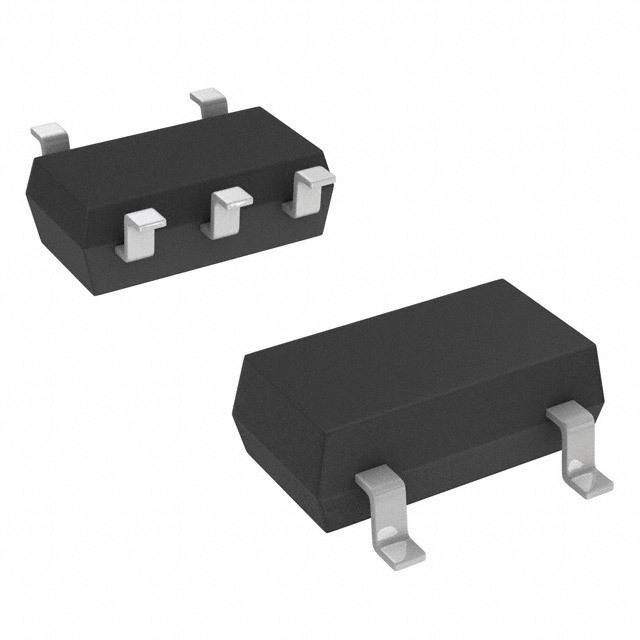
ICGOO电子元器件商城为您提供RT8009GJ5由RICHTEK设计生产,在icgoo商城现货销售,并且可以通过原厂、代理商等渠道进行代购。 RT8009GJ5价格参考。RICHTEKRT8009GJ5封装/规格:PMIC - 稳压器 - DC DC 开关稳压器, 可调式 降压 开关稳压器 IC 正 0.5V 1 输出 600mA SOT-23-5 细型,TSOT-23-5。您可以下载RT8009GJ5参考资料、Datasheet数据手册功能说明书,资料中有RT8009GJ5 详细功能的应用电路图电压和使用方法及教程。
| 参数 | 数值 |
| 产品目录 | 集成电路 (IC) |
| 描述 | IC REG BUCK SYNC ADJ TSOT23-5 |
| 产品分类 | |
| 品牌 | Richtek USA Inc |
| 数据手册 | http://www.richtek.com/download_ds.jsp?s=488 |
| 产品图片 |
|
| 产品型号 | RT8009GJ5 |
| PWM类型 | - |
| rohs | 无铅 / 符合限制有害物质指令(RoHS)规范要求 |
| RoHS指令信息 | http://www.richtek.com/download.jsp?t=UyUyRmFzc2V0cyUyRjIwMDklMkYwNiUyRjE3JTJGcGFnZTY1MTYwenRpeGIucGRmJTNEJTNEJTNE%0AR0w5NTI1LUMtLVBiLWZyZWUrUHJvZHVjdCsrR3JlZW4rUHJvZHVjdCtTdGF0ZW1lbnQrMDkwNjE2%0AQw%3D%3D |
| 产品系列 | - |
| 供应商器件封装 | TSOT-23-5 |
| 其它名称 | 1028-1026-1 |
| 其它有关文件 | |
| 包装 | 剪切带 (CT) |
| 同步整流器 | 是 |
| 安装类型 | 表面贴装 |
| 封装/外壳 | SOT-23-5 细型,TSOT-23-5 |
| 工作温度 | -40°C ~ 85°C |
| 标准包装 | 1 |
| 电压-输入 | 2.5 V ~ 5.5 V |
| 电压-输出 | 0.5 V ~ 5.5 V |
| 电流-输出 | 600mA |
| 类型 | 降压(降压) |
| 输出数 | 1 |
| 输出类型 | 可调式 |
| 频率-开关 | 1.25MHz |


- 商务部:美国ITC正式对集成电路等产品启动337调查
- 曝三星4nm工艺存在良率问题 高通将骁龙8 Gen1或转产台积电
- 太阳诱电将投资9.5亿元在常州建新厂生产MLCC 预计2023年完工
- 英特尔发布欧洲新工厂建设计划 深化IDM 2.0 战略
- 台积电先进制程称霸业界 有大客户加持明年业绩稳了
- 达到5530亿美元!SIA预计今年全球半导体销售额将创下新高
- 英特尔拟将自动驾驶子公司Mobileye上市 估值或超500亿美元
- 三星加码芯片和SET,合并消费电子和移动部门,撤换高东真等 CEO
- 三星电子宣布重大人事变动 还合并消费电子和移动部门
- 海关总署:前11个月进口集成电路产品价值2.52万亿元 增长14.8%


PDF Datasheet 数据手册内容提取
RT8009 1.25MHz, 600mA, High Efficiency PWM Step-Down DC/DC Converter General Description Features The RT8009 is a high-efficiency pulse-width-modulated (cid:122)(cid:122)(cid:122)(cid:122)(cid:122) 2.5V to 5.5V Input Range (PWM) step-down DC/DC converter. Capable of delivering (cid:122)(cid:122)(cid:122)(cid:122)(cid:122) Adjustable Output From 0.5V to VIN 600mA output current over a wide input voltage range from (cid:122)(cid:122)(cid:122)(cid:122)(cid:122) 1.0V, 1.2V, 1.3V, 1.5V, 1.8V, 2.5V and 3.3V Fixed/ 2.5 to 5.5V, the RT8009 is ideally suited for portable Adjustable Output Voltage electronic devices that are powered from 1-cell Li-ion (cid:122)(cid:122)(cid:122)(cid:122)(cid:122) 600mA Output Current battery or from other power sources within the range such (cid:122)(cid:122)(cid:122)(cid:122)(cid:122) 95% Efficiency as cellular phones, PDAs and handy-terminals. (cid:122)(cid:122)(cid:122)(cid:122)(cid:122) No Schottky Diode Required 1.25MHz Fixed Frequency PWM Operation (cid:122)(cid:122)(cid:122)(cid:122)(cid:122) Internal synchronous rectifier with low R dramatically DS(ON) Small SOT-23-5 and TSOT-23-5 Package (cid:122)(cid:122)(cid:122)(cid:122)(cid:122) reduces conduction loss at PWM mode. No external RoHS Compliant and 100% Lead (Pb)-Free (cid:122)(cid:122)(cid:122)(cid:122)(cid:122) Schottky diode is required in practical application. The RT8009 automatically turns off the synchronous rectifier Applications while the inductor current is low and enters discontinuous PWM mode. This can increase efficiency at light load (cid:122) Cellular Telephones condition. (cid:122) Personal Information Appliances Wireless and DSL Modems (cid:122) The RT8009 enters Low-Dropout mode when normal PWM MP3 Players (cid:122) cannot provide regulated output voltage by continuously Portable Instruments (cid:122) turning on the upper P-MOSFET. RT8009 enter shutdown mode and consumes less than 0.1μA when EN pin is pulled Ordering Information low. RT8009(- ) The switching ripple is easily smoothed-out by small Package Type package filtering elements due to a fixed operation B : SOT-23-5 J5 : TSOT-23-5 frequency of 1.25MHz. This along with small SOT-23-5 Lead Plating System and TSOT-23-5 package provides small PCB area P : Pb Free application. Other features include soft start, lower internal G : Green (Halogen Free and Pb Free) reference voltage with 2% accuracy, over temperature Output Voltage protection, and over current protection. Default : Adjustable 10 : 1.0V Pin Configurations 12 : 1.2V 13 : 1.3V (TOP VIEW) 15 : 1.5V LX FB/VOUT 18 : 1.8V 25 : 2.5V 5 4 33 : 3.3V 2 3 Note : VIN GND EN Richtek products are : SOT-23-5/TSOT-23-5 (cid:96) RoHS compliant and compatible with the current require- ments of IPC/JEDEC J-STD-020. Marking Information (cid:96) Suitable for use in SnPb or Pb-free soldering processes. For marking information, contact our sales representative directly or through a Richtek distributor located in your area. DS8009-07 March 2011 www.richtek.com 1
RT8009 Typical Application Circuit L 4.7µH VIN 1 VIN LX 5 VOUT 2.5V to 5.5V CIN 4.7µF RT8009 3 4 COUT EN VOUT 10µF GND 2 Figure 1. Fixed Voltage Regulator L ⎛ R1⎞ VIN 1 VIN LX 54.7µH VOUT VOUT = VREF x ⎜⎝1+R2⎟⎠ 2.5V to 5.5V CIN C1 with R1+R2≤1MΩ and 4.7µF RT8009 R1 VREF(Typ.)=0.5V 3 4 COUT EN FB 10µF GND R2 2 Figure 2. Adjustable Voltage Regulator Layout Guide VIN L VOUT VIN L VOUT VIN 1 5 LX VIN 1 5 LX C C C C IN OUT IN OUT GND 2 GND GND 2 GND R2 EN 3 4 VOUT EN 3 4 FB R1 VOUT C1 Figure 3 Layout note: 1.The distance that CIN connects to VIN is as close as possible (Under 2mm). 2. COUT should be placed near RT8009. www.richtek.com DS8009-07 March 2011 2
RT8009 Functional Pin Description Pin Number Pin Name Pin Function 1 VIN Power Input. 2 GND Ground. 3 EN Chip Enable (Active High, do not leave EN pin floating, and VEN < VIN + 0.6V). 4 FB/VOUT Feedback Input Pin. 5 LX Pin for Switching. Function Block Diagram EN VIN RS1 OSC & Current Shutdown Limit Control Detector Slope Compensation Current Sense Control Driver LX Logic PWM FB/VOUT Error Comparator Amplifier RC Zero UVLO & RS2 COMP Detector Power Good Detector V REF GND DS8009-07 March 2011 www.richtek.com 3
RT8009 Absolute Maximum Ratings (Note 1) Supply Input Voltage------------------------------------------------------------------------------------------------------ 6.5V (cid:122) Enable, FB Voltage ------------------------------------------------------------------------------------------------------- V + 0.6V (cid:122) IN Power Dissipation, P @ T = 25°C (cid:122) D A SOT-23-5, TSOT-23-5----------------------------------------------------------------------------------------------------- 0.4W Package Thermal Resistance (Note 2) (cid:122) SOT-23-5, TSOT-23-5, θ ----------------------------------------------------------------------------------------------- 250°C/W JA SOT-23-5, TSOT-23-5, θ ----------------------------------------------------------------------------------------------- 130°C/W JC Junction Temperature Range-------------------------------------------------------------------------------------------- 150°C (cid:122) Lead Temperature (Soldering, 10 sec.)------------------------------------------------------------------------------- 260°C (cid:122) Storage Temperature Range -------------------------------------------------------------------------------------------- −65°C to 150°C (cid:122) ESD Susceptibility (Note 3) (cid:122) HBM (Human Body Mode) ---------------------------------------------------------------------------------------------- 2kV MM (Machine Mode)------------------------------------------------------------------------------------------------------ 200V Recommended Operating Conditions (Note 4) Supply Input Voltage------------------------------------------------------------------------------------------------------ 2.5V to 5.5V (cid:122) Junction Temperature Range-------------------------------------------------------------------------------------------- −40°C to 125°C (cid:122) Ambient Temperature Range-------------------------------------------------------------------------------------------- −40°C to 85°C (cid:122) Electrical Characteristics (VIN = 3.6V, VOUT = 2.5V, VREF = 0.5V, L = 4.7μH, CIN= 4.7μF, COUT= 10μF, TA= 25°C, IMAX = 600mA unless otherwise specified) Parameter Symbol Test Conditions Min Typ Max Unit Input Voltage Range VIN 2.5 -- 5.5 V Quiescent Current I I = 0mA, V = V + 5% -- 50 100 μA Q OUT FB REF Shutdown Current ISHDN EN = GND -- 0.1 1 μA Reference Voltage V For adjustable output voltage 0.49 0.5 0.51 V REF Adjustable Output Range VOUT VREF -- VIN − 0.2 V VIN = 2.5 to 5.5V, VOUT = 1.0V ΔVOUT −3 -- 3 % 0A < IOUT < 600mA VIN = 2.5 to 5.5V, VOUT = 1.2V ΔVOUT −3 -- 3 % 0A < IOUT < 600mA V = 2.5 to 5.5V, V = 1.3V ΔVOUT IN OUT −3 -- 3 % 0A < IOUT < 600mA V = 2.5 to 5.5V, V = 1.5V ΔV IN OUT −3 -- 3 % OUT Output Voltage 0A < IOUT < 600mA Fix Accuracy V = 2.5 to 5.5V, V = 1.8V ΔV IN OUT −3 -- 3 % OUT 0A < I < 600mA OUT ΔV VIN = VOUT + ΔV to 5.5V (Note 5) −3 -- 3 % OUT V = 2.5V, 0A < I < 600mA OUT OUT V = V + ΔVto 5.5V (Note 5) ΔV IN OUT −3 -- 3 % OUT V = 3.3V, 0A < I < 600mA OUT OUT V = V + 0.2V to 5.5V ΔVOUT IN OUT −3 -- 3 % 0A < IOUT < 600mA To be continued www.richtek.com DS8009-07 March 2011 4
RT8009 Parameter Symbol Test Conditions Min Typ Max Unit OAcuctpuurat cVyo lta ge Adjustable ΔVOUT 0VAIN <= IOVOUTU T< +6 0Δ0Vm toA 5.5V (Note 5) −3 -- 3 % FB Input Current IFB VFB = VIN −50 -- 50 nA V = 3.6V -- 0.3 0.65 R of P-Channel MOSFET R I = 200mA IN Ω DS(ON) DS(ON)_P OUT VIN = 2.5V -- 0.4 0.80 V = 3.6V -- 0.25 0.55 R of N-Channel MOSFET R I = 200mA IN Ω DS(ON) DS(ON)_N OUT VIN = 2.5V -- 0.35 0.65 P-Channel Current Limit ILIM_P VIN = 2.5V to 5.5 V 1 -- 1.8 A EN High-Level Input Voltage V V = 2.5V to 5.5V 1.5 -- -- V EN_H IN EN Low-Level Input Voltage V V = 2.5V to 5.5V -- -- 0.4 V EN_L IN Under Voltage Lockout Threshold -- 1.8 -- V Hysteresis -- 0.1 -- V Oscillator Frequency fOSC VIN = 3.6V, IOUT = 100mA 0.8 1.25 1.85 MHz Thermal Shutdown Temperature TSD -- 160 -- °C Min. On Time -- 50 -- ns Max. Duty Cycle 100 -- -- % LX Leakage Current VIN = 3.6V, VLX = 0V or VLX = 3.6V −1 -- 1 μA Note 1. Stresses listed as the above “Absolute Maximum Ratings” may cause permanent damage to the device. These are for stress ratings. Functional operation of the device at these or any other conditions beyond those indicated in the operational sections of the specifications is not implied. Exposure to absolute maximum rating conditions for extended periods may remain possibility to affect device reliability. Note 2. θJA is measured in the natural convection at TA = 25°C on a low effective thermal conductivity test board of JEDEC 51-3 thermal measurement standard. Note 3. Devices are ESD sensitive. Handling precaution recommended. Note 4. The device is not guaranteed to function outside its operating conditions. Note 5. ΔV = IOUT x RDS(ON)_P DS8009-07 March 2011 www.richtek.com 5
RT8009 Typical Operating Characteristics Efficiency vs. Load Current Efficiency vs. Input Voltage 100 100 VIN = 3.3V 90 90 80 80 70 VIN = 5V 70 IOUT = 300mA IOUT = 600mA ) ) % % y ( 60 y ( 60 nc 50 nc 50 e e ci 40 ci 40 Effi Effi 30 30 20 20 10 10 VOUT = 1.8V VOUT = 1.8V 0 0 0.01 0.11 0.21 0.31 0.41 0.51 0.61 2.5 2.8 3.1 3.4 3.7 4 4.3 4.6 4.9 5.2 5.5 Load Current (A) Input Voltage (V) Load Regulation Current Limit vs. Input Voltage 1.810 2.50 2.25 1.805 2.00 ) V 1.800 ation ( 1.795 VIN = 5.5V VIN = 3.3V mit (A) 11..5705 Regul 1.790 VIN = 2.5V ent Li 11..0205 d 1.785 urr a C 0.75 o 1.780 L 0.50 1.775 0.25 VOUT = 1.8V VOUT = 1.8V 1.770 0.00 0.1 0.15 0.2 0.25 0.3 0.35 0.4 0.45 0.5 0.55 0.6 2.5 2.8 3.1 3.4 3.7 4 4.3 4.6 4.9 5.2 5.5 Load Current (A) Input Voltage (V) Frequency vs. Input Voltage Frequency vs. Temperature 1.26 1.26 1.24 1.24 z) ) 1 1.22 H 1.22 Hz M 1.20 M ncy ( 1.20 cy ( 1.18 e n u e q u 1.16 e 1.18 q r e F r F 1.14 1.16 1.12 VOUT = 1.8V VIN = 3.3V, VOUT = 1.8V 1.14 1.10 2.5 2.8 3.1 3.4 3.7 4 4.3 4.6 4.9 5.2 5.5 -50 -25 0 25 50 75 100 125 Input Voltage (V) Temperature (°C) www.richtek.com DS8009-07 March 2011 6
RT8009 Reference vs. Input Voltage Reference vs. Temperature 0.60 0.510 VOUT = 1.8V VIN = 3.3V, VOUT = 1.8V 0.58 0.508 0.56 0.505 0.54 ) ) V V e ( 0.52 e ( 0.503 c c n 0.50 n 0.500 e e r r efe 0.48 efe 0.498 R R 0.46 0.495 0.44 0.493 0.42 0.40 0.490 2.5 2.8 3.1 3.4 3.7 4 4.3 4.6 4.9 5.2 5.5 -50 -25 0 25 50 75 100 125 Input Voltage (V) Temperature (°C) Load Transient Response Load Transient Response VIN = 3.3V, VOUT = 1.8V, IOUT = 150mA to 600mA VIN = 3.3V, VOUT = 1.8V, IOUT = 300mA to 600mA VOUT VOUT (20mV/Div) (20mV/Div) IOUT IOUT (500mA/Div) (500mA/Div) Time (100μs/Div) Time (100μs/Div) Output Ripple Power On VIN = 3.3V, VOUT = 1.8V, IOUT = 600mA VIN = 3.3V, VOUT = 1.8V, IOUT = 600mA VOUT (2mV/Div) VEN (2V/Div) VLX VOUT (5V/Div) (1V/Div) ILX IIN (500mA/Div) (200mA/Div) Time (500ns/Div) Time (100μs/Div) DS8009-07 March 2011 www.richtek.com 7
RT8009 Applications Information The basic RT8009 application circuit is shown in Typical inductor ripple current and consequent output voltage ripple. Application Circuit. External component selection is Do not allow the core to saturate! determined by the maximum load current and begins with Different core materials and shapes will change the size/ the selection of the inductor value and operating frequency current and price/current relationship of an inductor. followed by C and C . IN OUT Toroid or shielded pot cores in ferrite or permalloy materials Inductor Selection are small and don’t radiate energy but generally cost more than powdered iron core inductors with similar For a given input and output voltage, the inductor value characteristics. The choice of which style inductor to use and operating frequency determine the ripple current. The ripple current ΔI increases with higher V and decreases mainly depends on the price vs size requirements and L IN any radiated field/EMI requirements. with higher inductance. ΔI = ⎡VOUT⎤⎡1− VOUT⎤ CIN and COUT Selection L ⎢⎣ f×L ⎥⎦⎢⎣ VIN ⎥⎦ The input capacitance, C , is needed to filter the IN trapezoidal current at the source of the top MOSFET. To Having a lower ripple current reduces the ESR losses in prevent large ripple voltage, a low ESR input capacitor the output capacitors and the output voltage ripple. Highest sized for the maximum RMS current should be used. RMS efficiency operation is achieved at low frequency with small current is given by : ripple current. This, however, requires a large inductor. V V A reasonable starting point for selecting the ripple current I =I OUT IN −1 RMS OUT(MAX) V V is ΔI = 0.4(I ). The largest ripple current occurs at the IN OUT L MAX This formula has a maximum at V = 2V , where I highest V . To guarantee that the ripple current stays IN OUT RMS IN = I /2. This simple worst-case condition is commonly below a specified maximum, the inductor value should be OUT used for design because even significant deviations do chosen according to the following equation : not offer much relief. Note that ripple current ratings from ⎡ V ⎤⎡ V ⎤ L= ⎢ OUT ⎥⎢1− OUT ⎥ capacitor manufacturers are often based on only 2000 ⎣f×ΔIL(MAX)⎦⎢⎣ VIN(MAX)⎥⎦ hours of life which makes it advisable to further derate the capacitor, or choose a capacitor rated at a higher Inductor Core Selection temperature than required. Several capacitors may also Once the value for L is known, the type of inductor must be paralleled to meet size or height requirements in the be selected. High efficiency converters generally cannot design. afford the core loss found in low cost powdered iron cores, The selection of C is determined by the effective series forcing the use of more expensive ferrite or mollypermalloy OUT resistance (ESR) that is required to minimize voltage ripple cores. Actual core loss is independent of core size for a and load step transients, as well as the amount of bulk fixed inductor value but it is very dependent on the capacitance that is necessary to ensure that the control inductance selected. As the inductance increases, core loop is stable. Loop stability can be checked by viewing losses decrease. Unfortunately, increased inductance the load transient response as described in a later section. requires more turns of wire and therefore copper losses The output ripple, ΔV , is determined by : will increase. OUT ⎡ 1 ⎤ Ferrite designs have very low core losses and are preferred ΔVOUT ≤ ΔIL ⎢ESR+ ⎥ ⎣ 8fCOUT⎦ at high switching frequencies, so design goals can concentrate on copper loss and preventing saturation. The output ripple is highest at maximum input voltage Ferrite core material saturates “hard”, which means that since ΔIL increases with input voltage. Multiple capacitors inductance collapses abruptly when the peak design placed in parallel may be needed to meet the ESR and current is exceeded. This results in an abrupt increase in RMS current handling requirements. Dry tantalum, special www.richtek.com DS8009-07 March 2011 8
RT8009 polymer, aluminum electrolytic and ceramic capacitors are Efficiency Considerations all available in surface mount packages. Special polymer The efficiency of a switching regulator is equal to the output capacitors offer very low ESR but have lower capacitance power divided by the input power times 100%. It is often density than other types. Tantalum capacitors have the useful to analyze individual losses to determine what is highest capacitance density but it is important to only limiting the efficiency and which change would produce use types that have been surge tested for use in switching the most improvement. Efficiency can be expressed as : power supplies. Aluminum electrolytic capacitors have Efficiency = 100% − (L1+ L2+ L3+ ...) significantly higher ESR but can be used in cost-sensitive where L1, L2, etc. are the individual losses as a percentage applications provided that consideration is given to ripple of input power. Although all dissipative elements in the current ratings and long term reliability. Ceramic capacitors circuit produce losses, two main sources usually account have excellent low ESR characteristics but can have a for most of the losses : VIN quiescent current and I2R high voltage coefficient and audible piezoelectric effects. losses. The VIN quiescent current loss dominates the The high Q of ceramic capacitors with trace inductance efficiency loss at very low load currents whereas the I2R can also lead to significant ringing. loss dominates the efficiency loss at medium to high load Using Ceramic Input and Output Capacitors currents. In a typical efficiency plot, the efficiency curve Higher values, lower cost ceramic capacitors are now at very low load currents can be misleading since the becoming available in smaller case sizes. Their high ripple actual power lost is of no consequence. current, high voltage rating and low ESR make them ideal 1. The VIN quiescent current is due to two components : for switching regulator applications. However, care must the DC bias current as given in the electrical characteristics be taken when these capacitors are used at the input and and the internal main switch and synchronous switch gate output. When a ceramic capacitor is used at the input charge currents. The gate charge current results from and the power is supplied by a wall adapter through long switching the gate capacitance of the internal power wires, a load step at the output can induce ringing at the MOSFET switches. Each time the gate is switched from input, VIN. At best, this ringing can couple to the output high to low to high again, a packet of charge ΔQ moves and be mistaken as loop instability. At worst, a sudden from V to ground. IN inrush of current through the long wires can potentially The resulting ΔQ/Δt is the current out of V that is typically IN cause a voltage spike at V large enough to damage the IN larger than the DC bias current. In continuous mode, part. I = f(Q +Q ) GATECHG T B Output Voltage Programming where Q and Q are the gate charges of the internal top The resistive divider allows the V pin to sense a fraction T B FB and bottom switches. Both the DC bias and gate charge of the output voltage as shown in Figure 4. losses are proportional to V and thus their effects will V IN OUT be more pronounced at higher supply voltages. R1 2. I2R losses are calculated from the resistances of the VFB internal switches, R and external inductor R . In SW L RT8009 R2 continuous mode the average output current flowing GND through inductor L is “chopped” between the main switch and the synchronous switch. Thus, the series resistance Figure 4. Setting the Output Voltage looking into the LX pin is a function of both top and bottom MOSFET R and the duty cycle (DC) as follows : For adjustable about voltage mode, the output voltage is DS(ON) set by an external resistive divider according to the following R = R x DC + R x (1−DC) SW DS(ON)TOP DS(ON)BOT equation : VOUT=VREF(1+ R1) The RDS(ON) for both the top and bottom MOSFETs can be R2 obtained from the Typical Performance Characteristics where V is the internal reference voltage (0.5V typ.) REF DS8009-07 March 2011 www.richtek.com 9
RT8009 curves. Thus, to obtain I2R losses, simply add R to R Where T is the package case (Pin 2 of package leads) SW L C and multiply the result by the square of the average output temperature measured by thermal sensor, P is the power D current. dissipation defined by user's function and the θ is the JC junction to case thermal resistance provided by IC Other losses including C and C ESR dissipative IN OUT manufacturer. Therefore it's easy to estimate the junction losses and inductor core losses generally account for less temperature by any condition. than 2% of the total loss. 450 Single Layer PCB ) Thermal Considerations W 400 m The maximum power dissipation depends on the thermal on ( 350 SOT-23-5, TSOT-23-5 Packages resistance of IC package, PCB layout, the rate of ati 300 p surroundings airflow and temperature difference between si s 250 junction to ambient. The maximum power dissipation can Di er 200 be calculated by following formula : w o 150 P PD(MAX) = ( TJ(MAX) - TA ) / θJA m 100 u m Where T is the maximum operation junction J(MAX) xi 50 temperature 125°C, TA is the ambient temperature and the Ma 0 θJA is the junction to ambient thermal resistance. 0 20 40 60 80 100 120 140 For recommended operating conditions specification of Ambient Temperature (°C) RT8009 DC/DC converter, where T is the maximum Figure 5. Derating Curves for RT8009 Package J (MAX) junction temperature of the die (125°C) and T is the A Checking Transient Response maximum ambient temperature. The junction to ambient thermal resistance θ is layout dependent. For The regulator loop response can be checked by looking JA SOT-23-5/TSOT-23-5 packages, the thermal resistance θ at the load transient response. Switching regulators take JA is 250°C/W on the standard JEDEC 51-3 single-layer several cycles to respond to a step in load current. When thermal test board. The maximum power dissipation at a load step occurs, VOUT immediately shifts by an amount TA = 25°C can be calculated by following formula : equal to ΔILOAD (ESR), where ESR is the effective series resistance of C . ΔI also begins to charge or P = ( 125°C - 25°C ) / 250 = 0.4 W for SOT-23-5/ OUT LOAD D(MAX) discharge C generating a feedback error signal used TSOT-23-5 packages OUT by the regulator to return V to its steady-state value. OUT The maximum power dissipation depends on operating During this recovery time, V can be monitored for OUT ambient temperature for fixed T and thermal J(MAX) overshoot or ringing that would indicate a stability problem. resistance θ . For RT8009 packages, the Figure 5 of JA derating curves allows the designer to see the effect of Layout Considerations rising ambient temperature on the maximum power Follow the PCB layout guidelines for optimal performance allowed. of RT8009. The value of junction to case thermal resistance θJC is (cid:96) For the main current paths as indicated in bold lines in popular for users. This thermal parameter is convenient Figure 6 keep their traces short and wide. for users to estimate the internal junction operated (cid:96) Put the input capacitor as close as possible to the device temperature of packages while IC operating. It's pins (VIN and GND). independent of PCB layout, the surroundings airflow effects and temperature difference between junction to ambient. (cid:96) LX node is with high frequency voltage swing and should be kept small area. Keep analog components away from The operated junction temperature can be calculated by LX node to prevent stray capacitive noise pick-up. following formula : T = T + P x θ J C D JC www.richtek.com DS8009-07 March 2011 10
RT8009 (cid:96) Connect feedback network behind the output capacitors. Keep the loop area small. Place the feedback components near the RT8009. (cid:96) Connect all analog grounds to a command node and then connect the command node to the power ground behind the output capacitors. (cid:96) An example of 2-layer PCB layout is shown in Figure 7 and Figure 8 for reference. Figure 7. Top Layer V V IN L1 OUT RT8009 1 5 VIN LX 4.7uH R3 C1 R1 3 4 EN FB C4 C3 C2 10uF R2 4.7uF GND 2 Figure 6. EVB Schematic Figure 8. Bottom Layer Recommended component selection for Typical Application Table 1. Inductors Component Supplier Series Inductance ( μH) DCR (mΩ) Current Rating (mA) Dimensions (mm) TAIYO YUDEN NR 3015 2.2 60 1480 3x3x1.5 TAIYO YUDEN NR 3015 4.7 120 1020 3x3x1.5 Sumida CDRH2D14 2.2 75 1500 4.5x3.2x1.55 Sumida CDRH2D14 4.7 135 1000 4.5x3.2x1.55 GOTREND GTSD32 2.2 58 1500 3.85x3.85x1.8 GOTREND GTSD32 4.7 146 1100 3.85x3.85x1.8 Table 2. Capacitors for C and C IN OUT Component Supplier Part No. Capacitance (μF) Case Size TDK C1608JB0J475M 4.7 0603 TDK C2012JB0J106M 10 0805 MURATA GRM188R60J475KE19 4.7 0603 MURATA GRM219R60J106ME19 10 0805 MURATA GRM219R60J106KE19 10 0805 TAIYO YUDEN JMK107BJ475RA 4.7 0603 TAIYO YUDEN JMK107BJ106MA 10 0603 TAIYO YUDEN JMK212BJ106RD 10 0805 DS8009-07 March 2011 www.richtek.com 11
RT8009 Outline Dimension H D L C B b A A1 e Dimensions In Millimeters Dimensions In Inches Symbol Min Max Min Max A 0.889 1.295 0.035 0.051 A1 0.000 0.152 0.000 0.006 B 1.397 1.803 0.055 0.071 b 0.356 0.559 0.014 0.022 C 2.591 2.997 0.102 0.118 D 2.692 3.099 0.106 0.122 e 0.838 1.041 0.033 0.041 H 0.080 0.254 0.003 0.010 L 0.300 0.610 0.012 0.024 SOT-23-5 Surface Mount Package www.richtek.com DS8009-07 March 2011 12
RT8009 H D L C B b A A1 e Dimensions In Millimeters Dimensions In Inches Symbol Min Max Min Max A 0.700 1.000 0.028 0.039 A1 0.000 0.100 0.000 0.004 B 1.397 1.803 0.055 0.071 b 0.300 0.559 0.012 0.022 C 2.591 3.000 0.102 0.118 D 2.692 3.099 0.106 0.122 e 0.838 1.041 0.033 0.041 H 0.080 0.254 0.003 0.010 L 0.300 0.610 0.012 0.024 TSOT-23-5 Surface Mount Package Richtek Technology Corporation Richtek Technology Corporation Headquarter Taipei Office (Marketing) 5F, No. 20, Taiyuen Street, Chupei City 5F, No. 95, Minchiuan Road, Hsintien City Hsinchu, Taiwan, R.O.C. Taipei County, Taiwan, R.O.C. Tel: (8863)5526789 Fax: (8863)5526611 Tel: (8862)86672399 Fax: (8862)86672377 Email: marketing@richtek.com Information that is provided by Richtek Technology Corporation is believed to be accurate and reliable. Richtek reserves the right to make any change in circuit design, specification or other related things if necessary without notice at any time. No third party intellectual property infringement of the applications should be guaranteed by users when integrating Richtek products into any application. No legal responsibility for any said applications is assumed by Richtek. DS8009-07 March 2011 www.richtek.com 13