ICGOO在线商城 > 分立半导体产品 > 晶体管 - FET,MOSFET - 单 > RSQ015P10TR

 Datasheet下载
- 型号: RSQ015P10TR
- 制造商: ROHM Semiconductor
- 库位|库存: xxxx|xxxx
- 要求:
| 数量阶梯 | 香港交货 | 国内含税 |
| +xxxx | $xxxx | ¥xxxx |
查看当月历史价格
查看今年历史价格
RSQ015P10TR产品简介:
ICGOO电子元器件商城为您提供RSQ015P10TR由ROHM Semiconductor设计生产,在icgoo商城现货销售,并且可以通过原厂、代理商等渠道进行代购。 RSQ015P10TR价格参考。ROHM SemiconductorRSQ015P10TR封装/规格:晶体管 - FET,MOSFET - 单, 表面贴装 P 沟道 100V 1.5A(Ta) 600mW(Ta) TSMT6(SC-95)。您可以下载RSQ015P10TR参考资料、Datasheet数据手册功能说明书,资料中有RSQ015P10TR 详细功能的应用电路图电压和使用方法及教程。
RSQ015P10TR 是由罗姆半导体(Rohm Semiconductor)生产的单通道 MOSFET(金属氧化物场效应晶体管)。这款晶体管属于增强型 N 沟道 MOSFET,具有低导通电阻和快速开关特性,适用于多种电力电子应用场景。以下是其主要应用场景:

 1. 电源管理
   RSQ015P10TR 可用于开关电源(SMPS)、DC-DC 转换器、降压/升压转换器等电源管理系统中。由于其低导通电阻(Rds(on)),在高频开关应用中能够减少功率损耗,提高效率。它还适用于电池充电电路中的开关控制,确保充电过程的安全性和稳定性。

 2. 电机驱动
   在小型电机驱动应用中,如步进电机、直流电机或无刷直流电机的驱动电路中,RSQ015P10TR 可作为功率级开关元件。通过精确控制栅极电压,可以实现对电机转速和方向的有效调节。其快速开关特性和低损耗有助于提高系统的响应速度和能效。

 3. 负载切换
   该 MOSFET 可用于负载切换电路中,例如在汽车电子系统、家用电器和其他需要频繁切换负载的应用中。RSQ015P10TR 的低导通电阻使其能够在高电流条件下保持较低的温升,从而延长设备的使用寿命。

 4. 保护电路
   RSQ015P10TR 还可用于过流保护、短路保护等电路设计中。通过检测电流并控制栅极电压,可以在异常情况下迅速切断电流路径,保护下游电路免受损坏。此外,其内置的体二极管可以在反向电流出现时提供一定的保护作用。

 5. 信号处理
   在某些模拟信号处理电路中,MOSFET 可用作开关或放大元件。RSQ015P10TR 的低噪声特性和高输入阻抗使其适合用于精密信号处理场景,如传感器接口、音频信号处理等。

 总结
RSQ015P10TR 凭借其优异的电气性能和可靠性,广泛应用于电源管理、电机驱动、负载切换、保护电路以及信号处理等领域。它特别适用于需要高效、快速响应和低功耗的场合,能够显著提升系统的整体性能和可靠性。
| 参数 | 数值 |
| 产品目录 | |
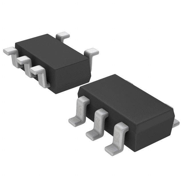
| 描述 | MOSFET P-CH 100V 1.5A TSMT6 |
| 产品分类 | FET - 单 |
| FET功能 | 逻辑电平栅极,4V 驱动 |
| FET类型 | MOSFET P 通道,金属氧化物 |
| 品牌 | Rohm Semiconductor |
| 数据手册 | |
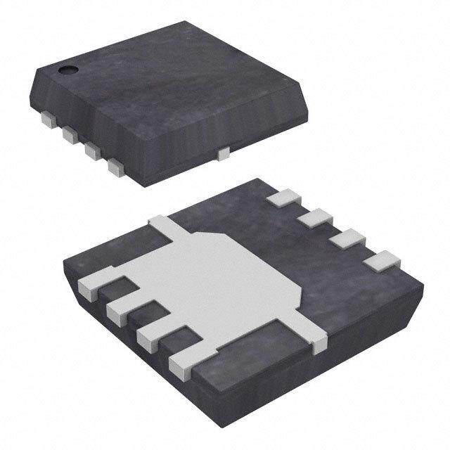
| 产品图片 |
|
| 产品型号 | RSQ015P10TR |
| rohs | 无铅 / 符合限制有害物质指令(RoHS)规范要求 |
| 产品系列 | - |
| 不同Id时的Vgs(th)(最大值) | 2.5V @ 1mA |
| 不同Vds时的输入电容(Ciss) | 950pF @ 25V |
| 不同Vgs时的栅极电荷(Qg) | 17nC @ 5V |
| 不同 Id、Vgs时的 RdsOn(最大值) | 470 毫欧 @ 1.5A,10V |
| 供应商器件封装 | TSMT6 |
| 其它名称 | RSQ015P10TRDKR |
| 功率-最大值 | 1.25W |
| 包装 | Digi-Reel® |
| 安装类型 | 表面贴装 |
| 封装/外壳 | SOT-23-6 细型,TSOT-23-6 |
| 标准包装 | 1 |
| 漏源极电压(Vdss) | 100V |
| 电流-连续漏极(Id)(25°C时) | 1.5A (Ta) |


PDF Datasheet 数据手册内容提取
RSQ015P10 Pch -100V -1.5A Power MOSFET Data Sheet lOutline V -100V (6) DSS TSMT6 (5) R (Max.) 470mW (4) DS(on) I -1.5A D (1) (2) P 1.25W D (3) lFeatures lInner circuit 1) Low on - resistance. (1) Drain 2) Built-in G-S Protection Diode. (2) Drain (3) Gate (4) Source 3) Small Surface Mount Package (TSMT6). (5) Drain (6) Drain 4) Pb-free lead plating ; RoHS compliant *1 ESD PROTECTION DIODE *2 BODY DIODE lPackaging specifications Packaging Taping Reel size (mm) 180 lApplication Tape width (mm) 8 DC/DC converters Type Basic ordering unit (pcs) 3,000 Taping code TR Marking ZN lAbsolute maximum ratings(T = 25°C) a Parameter Symbol Value Unit Drain - Source voltage V -100 V DSS Continuous drain current I *1 1.5 A D Pulsed drain current I *2 6.0 A D,pulse Gate - Source voltage V 20 V GSS P *3 1.25 W D Power dissipation P *4 0.6 W D Junction temperature T 150 °C j Range of storage temperature T -55 to +150 °C stg www.rohm.com © 2014 ROHM Co., Ltd. All rights reserved. 1/11 2014.05 - Rev.C
RSQ015P10 Data Sheet lThermal resistance Values Parameter Symbol Unit Min. Typ. Max. R *3 - - 100 °C/W thJA Thermal resistance, junction - ambient R *4 - - 208 °C/W thJA lElectrical characteristics(T = 25°C) a Values Parameter Symbol Conditions Unit Min. Typ. Max. Drain - Source breakdown V V = 0V, I = -1mA -100 - - V voltage (BR)DSS GS D Breakdown voltage ΔV I = -1mA (BR)DSS D - -109 - mV/°C temperature coefficient ΔT referenced to 25°C j Zero gate voltage drain current I V = -100V, V = 0V - - -1 mA DSS DS GS Gate - Source leakage current I V = 20V, V = 0V - - 10 mA GSS GS DS Gate threshold voltage V V = -10V, I = -1mA -1.0 - -2.5 V GS (th) DS D Gate threshold voltage ΔV I = -1mA (GS)th D - 3.2 - mV/°C temperature coefficient ΔT referenced to 25°C j V = -10V, I = -1.5A - 350 470 GS D V = -4.5V, I = -0.75A - 380 510 Static drain - source GS D R *5 mW on - state resistance DS(on) V = -4.0V, I = -0.75A - 400 540 GS D V = -10V, I = -1.5A, T=125C - 610 850 GS D j Gate input resistannce R f = 1MHz, open drain - 8.5 - W G Transconductance g *5 V = -10V, I = -1.5A 1.5 4.0 - S fs DS D *1 Limited only by maximum temperature allowed. *2 Pw 10ms, Duty cycle 1% *3 Mounted on a ceramic board (30×30×0.8mm) *4 Mounted on a FR4 (15×20×0.8mm) *5 Pulsed www.rohm.com © 2014 ROHM Co., Ltd. All rights reserved. 2/11 2014.05 - Rev.C
RSQ015P10 Data Sheet lElectrical characteristics(T = 25°C) a Values Parameter Symbol Conditions Unit Min. Typ. Max. Input capacitance C V = 0V - 950 - iss GS Output capacitance C V = -25V - 45 - pF oss DS Reverse transfer capacitance C f = 1MHz - 20 - rss Turn - on delay time t *5 V ⋍ -50V, V = -10V - 10 - d(on) DD GS Rise time t *5 I = -0.75A - 15 - r D ns Turn - off delay time t *5 R = 66W - 60 - d(off) L Fall time t *5 R = 10W - 10 - f G lGate Charge characteristics(T = 25°C) a Values Parameter Symbol Conditions Unit Min. Typ. Max. V ⋍ -50V, I = -1.5A DD D - 17.0 - V = -5V GS Total gate charge Q *5 g V ⋍ -50V, I = -1.5A DD D - 32 - nC V = -10V GS Gate - Source charge Qgs *5 VDD ⋍ -50V, ID= -1.5A - 4.5 - Gate - Drain charge Q *5 VGS = -5V - 5.0 - gd lBody diode electrical characteristics (Source-Drain)(T = 25°C) a Values Parameter Symbol Conditions Unit Min. Typ. Max. Inverse diode continuous, I *1 T = 25°C - - -1.0 A forward current S a Forward voltage V *5 V = 0V, I = -1.5A - - -1.2 V SD GS s www.rohm.com © 2014 ROHM Co., Ltd. All rights reserved. 3/11 2014.05 - Rev.C
RSQ015P10 Data Sheet lElectrical characteristic curves Fig.1 Power Dissipation Derating Curve Fig.2 Maximum Safe Operating Area 120 100 Operation in this area P = 100ms x. [%] 100 10 is lim(VitGeSd = b -y 1R0DVS)( on) W PW = 1ms a m 80 A] P D [D 1 ation : P/D 4600 Current : -I 0.1 PW =D 1C0 Ompse ration p n Dissi Drai 0.01 Ta=25ºC r 20 Single Pulse e w Mounted on a ceramic board. o (30mm × 30mm × 0.8mm) P 0 0.001 0 50 100 150 200 0.1 1 10 100 1000 Junction Temperature : Tj [°C] Drain - Source Voltage : -V [V] DS Fig.3 Normalized Transient Thermal Fig.4 Single Pulse Maxmum Resistance vs. Pulse Width Power dissipation e : r(t) 10 TSain=g2l5eº CPu lse 1000 TSain=g2l5eº CPu lse c an ) st 1 W si P( Re : 100 al er m top D = 1 w er 0.1 D = 0.5 Po Th D = 0.1 nt ent DD == 00..0051 nsie 10 si bottom Single a n 0.01 r a T Tr Rth(ch-a)=100ºC/W k d Rth(ch-a)(t)=r(t)×Rth(ch-a) ea e Mounted on ceramic board P z ali 0.001 (30mm × 30mm × 0.8mm) 1 m r 0.0001 0.01 1 100 0.0001 0.01 1 100 o N Pulse Width : P [s] Pulse Width : P [s] W W www.rohm.com © 2014 ROHM Co., Ltd. All rights reserved. 4/11 2014.05 - Rev.C
RSQ015P10 Data Sheet lElectrical characteristic curves Fig.5 Typical Output Characteristics(I) Fig.6 Typical Output Characteristics(II) 1.5 1.5 VGS= -10.0V VGS= -10.0V VGS= -4.5V VGS= -4.5V A] 1 VGS= -4.0V VGS= -2.8V A] 1 VGS= -4.0V [D [D -I -I nt : nt : VGS= -2.8V e e r r r r u u n C 0.5 n C 0.5 VGS= -2.5V rai VGS= -2.5V rai D D T =25ºC T =25ºC a a Pulsed Pulsed 0 0 0 0.2 0.4 0.6 0.8 1 0 2 4 6 8 10 Drain - Source Voltage : -V [V] Drain - Source Voltage : -V [V] DS DS Fig.7 Breakdown Voltage Fig.8 Typical Transfer Characteristics vs. Junction Temperature V] 160 10 [SS VGS = 0V VDS= -10V D 140 I = -1mA Pulsed R) D B Pulsed V( 120 1 - e : A] T = 125ºC ag 100 [D Ta= 75ºC wn Volt 80 ent : -I 0.1 TTaaa== 2-255ºCºC r do 60 Cur k a n re 40 ai 0.01 B r e D rc 20 u o S - 0 0.001 n -50 0 50 100 150 0.0 0.5 1.0 1.5 2.0 2.5 3.0 3.5 ai r D Junction Temperature : T [°C] Gate - Source Voltage : -V [V] j GS www.rohm.com © 2014 ROHM Co., Ltd. All rights reserved. 5/11 2014.05 - Rev.C
RSQ015P10 Data Sheet lElectrical characteristic curves Fig.9 Gate Threshold Voltage Fig.10 Transconductance vs. Drain Current vs. Junction Temperature 3 10 V = -10V DS V] Pulsed [S(th) S] VG 2 [s 1 - gf e : e : g c Volta uctan TTaa==2 -52º5Cº C hreshold 1 VDS = -10V anscond 0.1 TTaa==71525ºCºC T I = -1mA Tr e D at Pulsed G 0 0.01 -50 0 50 100 150 0.001 0.01 0.1 1 10 Junction Temperature : T [°C] Drain Current : -I [A] j D Fig.11 Drain CurrentDerating Curve Fig.12 Static Drain - Source On - State Resistance vs. Gate Source Voltage 1.2 e c T =25ºC n a a Pulsed 1 sist ID = -1.5A n e o R sipati%) 0.8 State ] W ID = -0.75A ain Current Dis: I/Imax. (D D 00..46 n - Source On-: R [mDS(on) Dr 0.2 ai r D c 0 ati -25 0 25 50 75 100 125 150 St Junction Temperature : T [ºC] Gate - Source Voltage : -V [V] j GS www.rohm.com © 2014 ROHM Co., Ltd. All rights reserved. 6/11 2014.05 - Rev.C
RSQ015P10 Data Sheet lElectrical characteristic curves Fig.13 Static Drain - Source On - State Fig.14 Static Drain - Source On - State Resistance vs. Drain Current(I) Resistance vs. Junction Temperature 1000 700 e T =25ºC e c a c an Pulsed V = -4.0V an 600 st GS st esi VGS= -4.5V esi R VGS= -10V R 500 e e Stat] W Stat] W 400 -m -m n n e O [on) e O [on) 300 c S( c S( r D r D uR uR So: So: 200 - - ain ain 100 VI G =S =- 1-.150AV Dr Dr D Pulsed c c ati 100 ati 0 St 0.01 0.1 1 10 St -50 -25 0 25 50 75 100 125 150 Drain Current : -I [A] Junction Temperature : T [ºC] D j Fig.15 Static Drain - Source On - State Fig.16 Static Drain-Source On-State Resistance vs. Drain Current(II) Resistance vs. Drain Current(III) State Resistance ] W110000000 VPGuSls=e -d1 0V TTTTaaaa====172 -25525ºº5CCººC C -State Resistance m] W110000000 VPGuSls=e -d4 .5V TTTTaaaa====172 -25525ºº5CCººC C ce On- [mS(on) rce On [DS(on) ain - Sour: RD 100 rain - Sou: R 100 r D Static D 100.01 0.1 1 10 Static 100.01 0.1 1 10 Drain Current : -I [A] Drain Current : -I [A] D D www.rohm.com © 2014 ROHM Co., Ltd. All rights reserved. 7/11 2014.05 - Rev.C
RSQ015P10 Data Sheet lElectrical characteristic curves Fig.17 Static Drain - Source On - State Fig.18 Typical Capacitance Resistance vs. Drain Current(IV) vs. Drain - Source Voltage e 10000 10000 anc VPGuSls=e -d4 .0V Ta=125ºC sist TTa==7255ººCC e a 1000 R T = -25ºC State ] W 1000 a C [pF] Ciss -m Source On: R [DS(on) 100 acitance : 100 Coss n - Cap 10 ai Ta = 25ºC C Dr f = 1MHz rss atic 10 1 VGS = 0V St 0.01 0.1 1 10 0.01 1 100 Drain Current : -I [A] Drain - Source Voltage : -V [V] D DS Fig.19 Switching Characteristics Fig.20 Dynamic Input Characteristics 10000 10 T =25ºC a V ≒ -50V DD t VGS= -10V V] 8 1000 f RG=10W [S s] Pulsed VG n t - Time : t [ 100 d(off) Voltage : 6 g td(on) e 4 n c hi ur Switc 10 e - So 2 TVaD=D2=5 -ºC50 V tr Gat IPDu=l s-e1d.5 A 1 0 0.01 0.1 1 10 0 5 10 15 20 25 30 35 Drain Current : -I [A] Total Gate Charge : Q [nC] D g www.rohm.com © 2014 ROHM Co., Ltd. All rights reserved. 8/11 2014.05 - Rev.C
RSQ015P10 Data Sheet lElectrical characteristic curves Fig.21 Source Current vs. Source Drain Voltage 10 V =0V GS Pulsed T =125ºC A] Ta=75ºC [S 1 Ta=25ºC nt : -I Taa= -25ºC e r r u C e 0.1 c r u o S 0.01 0.0 0.5 1.0 1.5 2.0 Source-Drain Voltage : -V [V] SD www.rohm.com © 2014 ROHM Co., Ltd. All rights reserved. 9/11 2014.05 - Rev.C
RSQ015P10 Data Sheet lMeasurement circuits Fig.1-1 Switching Time Measurement Circuit Fig.1-2 Switching Waveforms Fig.2-1 Gate Charge Measurement Circuit Fig.2-2 Gate Charge Waveform www.rohm.com © 2014 ROHM Co., Ltd. All rights reserved. 10/11 2014.05 - Rev.C
RSQ015P10 Data Sheet lDimensions (Unit : mm) D A e TSMT6 c Q E E H 1 p L L b x S A A3 e 2 1 A A e y S 1 1 A l S b2 Patterm of terminal position areas MILIMETERS INCHES DIM MIN MAX MIN MAX A - 1.00 - 0.039 A1 0.00 0.10 0 0.004 A2 0.75 0.95 0.03 0.037 A3 0.25 0.01 b 0.35 0.50 0.014 0.02 c 0.10 0.26 0.004 0.01 D 2.80 3.00 0.11 0.118 E 1.50 1.80 0.059 0.071 e 0.95 0.04 HE 2.60 3.00 0.102 0.118 L1 0.30 0.60 0.012 0.024 Lp 0.40 0.70 0.016 0.028 Q 0.05 0.25 0.002 0.01 x - 0.20 - 0.008 y - 0.10 - 0.004 MILIMETERS INCHES DIM MIN MAX MIN MAX e1 2.10 0.08 b2 0.70 - 0.028 l1 - 0.90 - 0.035 Dimension in mm/inches www.rohm.com © 2014 ROHM Co., Ltd. All rights reserved. 11/11 2014.05 - Rev.C
Notice Notes 1) The information contained herein is subject to change without notice. 2) Before you use our Products, please contact our sales representative and verify the latest specifica- tions : 3) Although ROHM is continuously working to improve product reliability and quality, semicon- ductors can break down and malfunction due to various factors. Therefore, in order to prevent personal injury or fire arising from failure, please take safety measures such as complying with the derating characteristics, implementing redundant and fire prevention designs, and utilizing backups and fail-safe procedures. ROHM shall have no responsibility for any damages arising out of the use of our Poducts beyond the rating specified by ROHM. 4) Examples of application circuits, circuit constants and any other information contained herein are provided only to illustrate the standard usage and operations of the Products. The peripheral conditions must be taken into account when designing circuits for mass production. 5) The technical information specified herein is intended only to show the typical functions of and examples of application circuits for the Products. ROHM does not grant you, explicitly or implicitly, any license to use or exercise intellectual property or other rights held by ROHM or any other parties. ROHM shall have no responsibility whatsoever for any dispute arising out of the use of such technical information. 6) The Products are intended for use in general electronic equipment (i.e. AV/OA devices, communi- cation, consumer systems, gaming/entertainment sets) as well as the applications indicated in this document. 7) The Products specified in this document are not designed to be radiation tolerant. 8) For use of our Products in applications requiring a high degree of reliability (as exemplified below), please contact and consult with a ROHM representative : transportation equipment (i.e. cars, ships, trains), primary communication equipment, traffic lights, fire/crime prevention, safety equipment, medical systems, servers, solar cells, and power transmission systems. 9) Do not use our Products in applications requiring extremely high reliability, such as aerospace equipment, nuclear power control systems, and submarine repeaters. 10) ROHM shall have no responsibility for any damages or injury arising from non-compliance with the recommended usage conditions and specifications contained herein. 11) ROHM has used reasonable care to ensur the accuracy of the information contained in this document. However, ROHM does not warrants that such information is error-free, and ROHM shall have no responsibility for any damages arising from any inaccuracy or misprint of such information. 12) Please use the Products in accordance with any applicable environmental laws and regulations, such as the RoHS Directive. For more details, including RoHS compatibility, please contact a ROHM sales office. ROHM shall have no responsibility for any damages or losses resulting non-compliance with any applicable laws or regulations. 13) When providing our Products and technologies contained in this document to other countries, you must abide by the procedures and provisions stipulated in all applicable export laws and regulations, including without limitation the US Export Administration Regulations and the Foreign Exchange and Foreign Trade Act. 14) This document, in part or in whole, may not be reprinted or reproduced without prior consent of ROHM. Thank you for your accessing to ROHM product informations. More detail product informations and catalogs are available, please contact us. ROHM Customer Support System http://www.rohm.com/contact/ www.rohm.com R1102A © 2014 ROHM Co., Ltd. All rights reserved.