ICGOO在线商城 > RPI-131

 Datasheet下载
- 型号: RPI-131
- 制造商: ROHM Semiconductor
- 库位|库存: xxxx|xxxx
- 要求:
| 数量阶梯 | 香港交货 | 国内含税 |
| +xxxx | $xxxx | ¥xxxx |
查看当月历史价格
查看今年历史价格
RPI-131产品简介:
ICGOO电子元器件商城为您提供RPI-131由ROHM Semiconductor设计生产,在icgoo商城现货销售,并且可以通过原厂、代理商等渠道进行代购。 提供RPI-131价格参考¥14.30-¥19.18以及ROHM SemiconductorRPI-131封装/规格参数等产品信息。 你可以下载RPI-131参考资料、Datasheet数据手册功能说明书, 资料中有RPI-131详细功能的应用电路图电压和使用方法及教程。
| 参数 | 数值 |
| 产品目录 | |
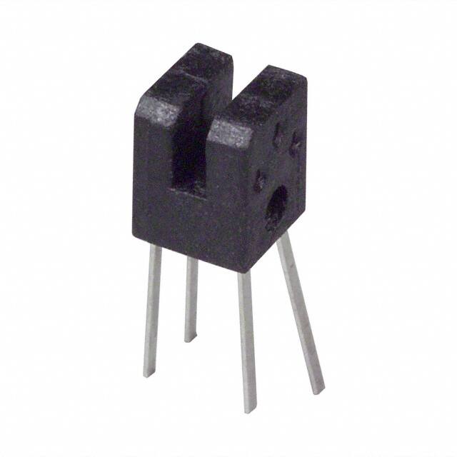
| 描述 | SENSR OPTO SLOT 1.2MM TRANS THRU光学开关(透射型,光电晶体管输出) 0.40mm slit width 0.7mA min., 5V |
| 产品分类 | |
| 品牌 | ROHM Semiconductor |
| 产品手册 | |
| 产品图片 |
|
| rohs | 符合RoHS无铅 / 符合限制有害物质指令(RoHS)规范要求 |
| 产品系列 | 光学开关(透射型,光电晶体管输出),ROHM Semiconductor RPI-131- |
| 数据手册 | |
| 产品型号 | RPI-131 |
| 上升时间 | 10 us |
| 下降时间 | 10 us |
| 产品目录页面 | |
| 产品种类 | 光学开关(透射型,光电晶体管输出) |
| 光圈宽度 | 0.4 mm |
| 其它名称 | 511-1339 |
| 功率耗散 | 80 mW |
| 包装 | 散装 |
| 响应时间 | 10µs, 10µs |
| 商标 | ROHM Semiconductor |
| 安装类型 | 通孔 |
| 封装 | Bulk |
| 封装/外壳 | PCB 安装 |
| 工作温度 | -25°C ~ 85°C |
| 工厂包装数量 | 2000 |
| 感应方式 | Transmissive, Slotted |
| 感应方法 | 可传导的 |
| 感应距离 | 0.047"(1.2mm) |
| 最大工作温度 | + 85 C |
| 最大集电极电流 | 30 mA |
| 最小工作温度 | - 25 C |
| 标准包装 | 2,000 |
| 槽宽 | 1.2 mm |
| 正向电流 | 50 mA |
| 波长 | 950 nm |
| 电压-集射极击穿(最大值) | 30V |
| 电流-DC正向(If) | 50mA |
| 电流-集电极(Ic)(最大值) | 30mA |
| 类型 | 无放大 |
| 输出设备 | Phototransistor |
| 输出配置 | 光电晶体管 |
| 集电极—发射极最大电压VCEO | 30 V |


- 商务部:美国ITC正式对集成电路等产品启动337调查
- 曝三星4nm工艺存在良率问题 高通将骁龙8 Gen1或转产台积电
- 太阳诱电将投资9.5亿元在常州建新厂生产MLCC 预计2023年完工
- 英特尔发布欧洲新工厂建设计划 深化IDM 2.0 战略
- 台积电先进制程称霸业界 有大客户加持明年业绩稳了
- 达到5530亿美元!SIA预计今年全球半导体销售额将创下新高
- 英特尔拟将自动驾驶子公司Mobileye上市 估值或超500亿美元
- 三星加码芯片和SET,合并消费电子和移动部门,撤换高东真等 CEO
- 三星电子宣布重大人事变动 还合并消费电子和移动部门
- 海关总署:前11个月进口集成电路产品价值2.52万亿元 增长14.8%


PDF Datasheet 数据手册内容提取
RPI-131 Sensors Photointerrupter, double-layer mold type RPI-131 The RPI-131 is an ultra-small size, double-layer photointerrupter. (cid:122)(cid:122)(cid:122)(cid:122)Applications (cid:122)(cid:122)(cid:122)(cid:122)External dimensions (Units : mm) Optical control equipment Cameras 4.2 N1.o Utenss:pecified tolerance Floppy disk drives shall be ±0.2. 4.2 2. sDhimowe nfosiro rne fienr peanrceen.thesis are Cross-section A-A (cid:122)(cid:122)(cid:122)(cid:122)Features 1A.2 0.4 C0.5 12)) MUlitnraim-saml ianlfll.uence from stray light. 5.22.8 1.31Opticacel anxt(1.2)eisr φ1.5+−00.1 3) Low collector-emitter saturation voltage. Min.5 A (1.5) 2−0.2 (2.5) 0.5 (3.2) Anode Collector Cathode Emitter (cid:122)(cid:122)(cid:122)(cid:122)Absolute maximum ratings (Ta = 25°C) Parameter Symbol Limits Unit )D Forward current IF 50 mA E (utL Reverse voltage VR 5 V np Power dissipation PD 80 mW I Collector-emitter voltage VCEO 30 V Output)(photo-transistor ECCmoollillteeteccttroo-crr ocpluloerwcreteonrr t dviossltiapgaetion VPIECCCO 438.005 mmVWA Operating temperature Topr −25~+85 °C Storage temperature Tstg −40~+100 °C
RPI-131 Sensors (cid:122)(cid:122)(cid:122)(cid:122)Electrical and optical characteristics (Ta = 25°C) Parameter Symbol Min. Typ. Max. Unit Conditions Inputcharac-teristics RFoervwearsrde vcoulrtraegnet VIRF −− 1−.3 11.06 µVA IVF=R=550VmA Outputcharac-teristics PDeaarkk csuernresnititvity wavelength ICλEPO −− 80−0 0−.5 nµmA VCE=10V − IC1 0.7 − − mA VCE=5V, IF=20mA Collector current Transfercharac-teristics Cvoolltlaegcetor-emitter saturation VCIEC(2sat) 0−.2 −− 0−.3 mVA VIF=CE2=05mVA, ,I FI=C5=m0.3mA Response time tr · tf − 10 − µs VCC=5V, IF=20mA, RL=100Ω (cid:122)(cid:122)(cid:122)(cid:122)Electrical and optical characteristic curves W) 5 P (mC120 A) 50 −7255°°CC A) TION / WER DISSIPATION : P/ D 146800000 PD PC WARD CURRENT : I (mF 234000 752505°°°CCC CTOR CURRENT : I (mC 234 OWER DISSIPAOLLECTOR PO 200−20 0 20 40 60 80 100 FOR 1000.2 0.4 0.6 0.8 1.0 1.2 1.4 1.6 1.8 COLLE 010 10 20 30 40 50 PC AMBIENT TEMPERATURE : Ta (°C) FORWARD VOLTAGE : VF (V) FORWARD CURRENT : IF (mA) Fig.1 Power dissipation / collector power Fig.2 Forward current vs. forward voltage Fig.3 Collector current vs. forward current dissipation vs. ambient temperature NT : I (nA)CEO110100000 VVVCCCEEE===321000VVV OR CURRENT : I (%)C11118602400000 OR CURRENT : I (%)C1608000 Shield pldate RE CT CT CUR 1 OLLE 60 OLLE 40 DARK 0.1 −25 0 25 50 75 100 RELATIVE C 24000 −40 −20 0 20 40 60 80 100 RELATIVE C 2000 1 2 3 4 5 6 AMBIENT TEMPERATURE : Ta (°C) AMBIENT TEMPERATURE : Ta (°C) DISTANCE : d (mm) Fig.4 Dark current Fig.5 Relative output vs. ambient Fig.6 Relative output current vs. Fig.4 vs. ambient temperature temperature distance
RPI-131 Sensors 1000 Ta=25°C µRESPONSE TIME : t (s)r11000 RRRLLL===V511C0k0CΩ00=ΩΩ5V RWARD CURRENT : I (mA)F 54320000 LECTOR CURRENT : I (mA)C 2143 IF=22115005mmmmAAAA FO 10 OL C 5mA 10.1 1 10 100 0−20 0 20 40 60 80 100 00 2 4 6 8 10 COLLECTOR CURRENT : IC (mA) AMBIENT TEMPERATURE : Ta (°C) COLLECTOR-EMITTER VOLTAGE : VCE (V) Fig.7 Response time vs. Fig.8 Forward current falloff Fig.9 Output characteristics collector current Input VCC Input Output 90% RL Output 10% td tr tf td : Delay time tr : Rise time (time for output current to rise from 10% to 90% of peak current) tf : Fall time (time for output current to fall from 90% to 10% of peak current) Fig.10 Response time measurement circuit
Appendix Notes No technical content pages of this document may be reproduced in any form or transmitted by any means without prior permission of ROHM CO.,LTD. The contents described herein are subject to change without notice. The specifications for the product described in this document are for reference only. Upon actual use, therefore, please request that specifications to be separately delivered. Application circuit diagrams and circuit constants contained herein are shown as examples of standard use and operation. Please pay careful attention to the peripheral conditions when designing circuits and deciding upon circuit constants in the set. Any data, including, but not limited to application circuit diagrams information, described herein are intended only as illustrations of such devices and not as the specifications for such devices. ROHM CO.,LTD. disclaims any warranty that any use of such devices shall be free from infringement of any third party's intellectual property rights or other proprietary rights, and further, assumes no liability of whatsoever nature in the event of any such infringement, or arising from or connected with or related to the use of such devices. Upon the sale of any such devices, other than for buyer's right to use such devices itself, resell or otherwise dispose of the same, no express or implied right or license to practice or commercially exploit any intellectual property rights or other proprietary rights owned or controlled by ROHM CO., LTD. is granted to any such buyer. Products listed in this document use silicon as a basic material. Products listed in this document are no antiradiation design. The products listed in this document are designed to be used with ordinary electronic equipment or devices (such as audio visual equipment, office-automation equipment, communications devices, electrical appliances and electronic toys). Should you intend to use these products with equipment or devices which require an extremely high level of reliability and the malfunction of with would directly endanger human life (such as medical instruments, transportation equipment, aerospace machinery, nuclear-reactor controllers, fuel controllers and other safety devices), please be sure to consult with our sales representative in advance. About Export Control Order in Japan Products described herein are the objects of controlled goods in Annex 1 (Item 16) of Export Trade Control Order in Japan. In case of export from Japan, please confirm if it applies to "objective" criteria or an "informed" (by MITI clause) on the basis of "catch all controls for Non-Proliferation of Weapons of Mass Destruction. Appendix1-Rev1.0