ICGOO在线商城 > RM3216A-102/502-PBVW10

 Datasheet下载
- 型号: RM3216A-102/502-PBVW10
- 制造商: SUSUMU INTERNATIONAL
- 库位|库存: xxxx|xxxx
- 要求:
| 数量阶梯 | 香港交货 | 国内含税 |
| +xxxx | $xxxx | ¥xxxx |
查看当月历史价格
查看今年历史价格
RM3216A-102/502-PBVW10产品简介:
ICGOO电子元器件商城为您提供RM3216A-102/502-PBVW10由SUSUMU INTERNATIONAL设计生产,在icgoo商城现货销售,并且可以通过原厂、代理商等渠道进行代购。 提供RM3216A-102/502-PBVW10价格参考以及SUSUMU INTERNATIONALRM3216A-102/502-PBVW10封装/规格参数等产品信息。 你可以下载RM3216A-102/502-PBVW10参考资料、Datasheet数据手册功能说明书, 资料中有RM3216A-102/502-PBVW10详细功能的应用电路图电压和使用方法及教程。
| 参数 | 数值 |
| 产品目录 | |
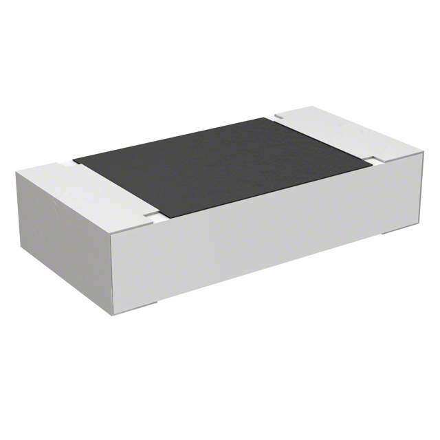
| 描述 | RES NET MULT OHM 2 RES 1206电阻器网络与阵列 1K/5K 25V |
| 产品分类 | |
| 品牌 | Susumu |
| 产品手册 | |
| 产品图片 |
|
| rohs | 符合RoHS无铅 / 符合限制有害物质指令(RoHS)规范要求 |
| 产品系列 | 电阻器网络与阵列,Susumu RM3216A-102/502-PBVW10RM |
| 数据手册 | |
| 产品型号 | RM3216A-102/502-PBVW10 |
| RoHS指令信息 | |
| 产品培训模块 | http://www.digikey.cn/PTM/IndividualPTM.page?site=cn&lang=zhs&ptm=7067 |
| 产品目录绘图 |
|
| 产品目录页面 | |
| 产品种类 | 电阻器网络与阵列 |
| 供应商器件封装 | 1206(3216 公制) |
| 其它名称 | RM32A1.0K/5.0KPDKR |
| 包装 | Digi-Reel® |
| 商标 | Susumu |
| 外壳宽度 | 1.6 mm |
| 外壳长度 | 3.2 mm |
| 外壳高度 | 0.4 mm |
| 大小/尺寸 | 0.126" 长 x 0.063" 宽(3.20mm x 1.60mm) |
| 安装类型 | 表面贴装 |
| 容差 | 0.1 % |
| 封装 | Reel |
| 封装/外壳 | 1206(3216 公制),长边端子 |
| 工作温度 | -55°C ~ 155°C |
| 工作温度范围 | - 55 C to + 155 C |
| 工厂包装数量 | 1000 |
| 应用 | - |
| 引脚数 | 4 |
| 标准包装 | 1 |
| 每元件功率 | 0.125 W (1/8 W) |
| 温度系数 | 25 PPM / C |
| 电压额定值 | 50 V |
| 电路类型 | 分压器 |
| 电阻(Ω) | 1k,5k |
| 电阻器数 | 2 |
| 电阻数值 | 1 kOhms, 5 kOhms |
| 端接类型 | SMD/SMT |
| 系列 | RM |
| 高度 | 0.020"(0.50mm) |


- 商务部:美国ITC正式对集成电路等产品启动337调查
- 曝三星4nm工艺存在良率问题 高通将骁龙8 Gen1或转产台积电
- 太阳诱电将投资9.5亿元在常州建新厂生产MLCC 预计2023年完工
- 英特尔发布欧洲新工厂建设计划 深化IDM 2.0 战略
- 台积电先进制程称霸业界 有大客户加持明年业绩稳了
- 达到5530亿美元!SIA预计今年全球半导体销售额将创下新高
- 英特尔拟将自动驾驶子公司Mobileye上市 估值或超500亿美元
- 三星加码芯片和SET,合并消费电子和移动部门,撤换高东真等 CEO
- 三星电子宣布重大人事变动 还合并消费电子和移动部门
- 海关总署:前11个月进口集成电路产品价值2.52万亿元 增长14.8%


PDF Datasheet 数据手册内容提取
Metal thin film chip resistor networks ■RM series AEC-Q200 Compliant Features ・Relative resistance tolerance and relative TCR definable among multiple resistors within package. ・Relative resistance tolerance: ±0.01%, relative TCR: ±1ppm/°C mount resistors ・・NaRvuGam islabeberilree osf ereqsuiisvtaolresn tin r eplaiacbkialitgye a: n2d olor nhgig theermr, ssttaabnidlitayr:d l easnsd tchuasnt o±m0. 1c%irc udirtisft daeftseigr ns Thin film surface ・1R0o0H0S0 choomurp sliatrnets, s1 t0e0s%t. lead free Applications ・Precision measurement instrumentation, medical electronics, automotive electronics s e eri ・Voltage divider and amplification circuits that require very precise relative resistance s M tolerance and TCR R ・Multi step precision amplification circuits for minute signals ◆Part numbering system RM 2012 A - ***/*** - P W X L 10 Packaging quantity: Series code 10(1,000pcs), 50(5,000pcs) Size: RM2012, RM3216, RM3225 Relative resistance tolerance circuits Relative TCR Absolute Nominal Resistance Value(R1/R2) TCR Absolute resistance tolerance RM 3216 C - *** - 10 Packaging quantity: Series code 10(1,000pcs), 50(5,000pcs) Size: RM3216, RM3225, RM6432 Custom part number (e.g.)N10 circuits ※Please contact our sales office regarding custom products including resistance, resistance combination, number of elements, circuit, and others. ※Standard quantity / reel is 1000 and 5000. Please contact our sales office for custom product's quantity / reel. ※Standard resistance value pairings are shown as below (Standard products are 2element circuit typeA & typeB only.) ◆Standard resistance value pairings Ratio R1(Ω)R2(Ω)Ratio R1(Ω)R2(Ω)Ratio R1(Ω)R2(Ω)Ratio R1(Ω)R2(Ω)Ratio R1(Ω)R2(Ω)Ratio R1(Ω)R2(Ω) 1k 1k 1k 3k 1k 5k 1k 9k 1k 20k 1K 50k 1 : 9 1 : 50 1 : 1 10k 10k 1 : 3 10k 30k 1 : 5 2k 10k 10k 90k 1 : 20 2k 40k 2K 100k 100k 100k 100k 300k 10k 50k 1k 10k 5k 100k 1K 100k 1:100 1k 2k 1k 4k 1k 6k 1 : 10 2k 20k 1k 25k 2K 200k 1 : 4 1 : 6 1 : 25 1 : 2 10k 20k 10k 40k 10k 60k 10k 100k 2k 50k 100k 200k 35
◆Electrical Specification ○ 4 terminal, 2 element Top view, terminal number Circuit diagram (circuit type A) Top view, terminal number Circuit diagram (circuit type B) ④ ③ ④ ③ ④ ③ ④ ③ R1 R2 R1 R2 ① ② ① ② ① ② ① ② Power Resistance Resistance tolerance (Code) Temperature coefficient of resistance (Code)*1 Pakaging Thin film Type r(a8t5in°Cgs) ra(Ωng)e tAoblesroalnuctee Relative tolerance*2 tAoblesroalnuctee Relative tolerance*2 (dqeusiagnnattiitoyn) surface m 0.05W / 100〜<300 ±±00..15%%((BD)) R±±±e00s 0ri..sa00.t1t5a2io%n%%c(e(B(WP=)))1 1<± R±0e 0s . ri0sa.1 tt5aio% n%c (e(BW≦)1)00100< Re s r isa-tt aion c e≦500±±1205ppppmm//℃℃((NP))±±R2e1sp prispapttmmaion//c℃℃e(=(WX1))1±±< R25e pps rpipsa mtmtaio n//c ℃℃ e≦((WV10))0100< Re s r isa-tt aion c e≦500 ount resistors ±0.5%(D) ±5ppm/℃(V) Element ±0.5%(D) RM2012 0.1W / ±0.05%(W) ±0.01%(L) ±0.02%(P) ±0.05%(W) ±5ppm/℃(V) ±1ppm/℃(X) ±1ppm/℃(X) Package ±2ppm/℃(W) 300〜100k ±±00..15%%((BD)) ±0.05±%0(W.5)% ±(D0).1%(B) ±±00..15%%((BD)) ±±1205ppppmm//℃℃((NP))±±25ppppmm//℃℃((WV)) ±±25ppppmm//℃℃((WV)) ±5ppm/℃(V) RM s e ±0.02%(P) ±0.05%(W) ±1ppm/℃(X) rie ±0.1%(B) ±0.05%(W) ±10ppm/℃(N) ±2ppm/℃(W) s 100〜<300 ±0.1%(B) - ±2ppm/℃(W) - tape & reel 0.083W / ±0.5%(D) ±0.1%(B) ±25ppm/℃(P) ±5ppm/℃(V) ±0.5%(D) ±5ppm/℃(V) Element ±0.5%(D) (T&R) RM3216 0.125W / ±0.05%(W) ±0.01%(L) ±0.02%(P) ±0.05%(W) ±5ppm/℃(V) ±1ppm/℃(X) ±1ppm/℃(X) 10=1,000pcs Package ±2ppm/℃(W) 300〜500k ±0.1%(B) ±0.05%(W) ±0.1%(B) ±0.1%(B) ±10ppm/℃(N)±2ppm/℃(W) ±2ppm/℃(W) 50=5,000pcs ±5ppm/℃(V) ±0.5%(D) ±0.5%(D) ±0.5%(D) ±25ppm/℃(P) ±5ppm/℃(V) ±5ppm/℃(V) ±0.02%(P) ±0.05%(W) ±1ppm/℃(X) ±0.1%(B) ±0.05%(W) ±10ppm/℃(N) ±2ppm/℃(W) 100〜<300 ±0.1%(B) - ±2ppm/℃(W) - 0.1W / ±0.5%(D) ±0.1%(B) ±25ppm/℃(P) ±5ppm/℃(V) ±0.5%(D) ±5ppm/℃(V) Element ±0.5%(D) RM3225 0.2W / ±0.05%(W) ±0.01%(L) ±0.02%(P) ±0.05%(W) ±5ppm/℃(V) ±1ppm/℃(X) ±1ppm/℃(X) Package ±2ppm/℃(W) 300〜500k ±0.1%(B) ±0.05%(W) ±0.1%(B) ±0.1%(B) ±10ppm/℃(N)±2ppm/℃(W) ±2ppm/℃(W) ±5ppm/℃(V) ±0.5%(D) ±0.5%(D) ±0.5%(D) ±25ppm/℃(P) ±5ppm/℃(V) ±5ppm/℃(V) *1 TCR guaranteed range : -20°C~ 125°C *2 Contact us for detailed information on relative tolerance and TCR. ○ 4 terminal, 3 element ○ 6 terminal, 3 element Top view, terminal number Circuit diagram (circuit type C) Circuit diagram (circuit type D) Circuit diagram (circuit type E) Top view, terminal number Circuit diagram (circuit type H) ④ ③ ④ ③ ④ ③ ④ ③ ⑥ ⑤ ④ ⑥ ⑤ ④ R1 R2 R1 R3 R3 R1 R1 R2 R3 R2 R2 R3 ① ② ① ② ① ② ① ② ① ② ③ ① ② ③ *1 Resistance tolerance (Code) Temperature coefficient of resistance (Code) Power Resistance Pakaging Type rating range *2 *2 quantity Absolute Relative tolerance Absolute Relative tolerance (85°C) (Ω) (designation) tolerance tolerance Res risattaionce=1 1< Re s risa ttaio nc e≦100100< Re s r isatt aion c e≦500 Res risattaionce=1 1< Re s risa ttaio nc e≦100100< Re s r isatt aion c e≦500 ±0.02%(P) ±0.05%(W) ±1ppm/℃(X) ±0.1%(B) ±0.05%(W) ±10ppm/℃(N) ±2ppm/℃(W) 100〜<300 ±0.1%(B) - ±2ppm/℃(W) - 0.042W / ±0.5%(D) ±0.1%(B) ±25ppm/℃(P) ±5ppm/℃(V) ±0.5%(D) ±5ppm/℃(V) Element ±0.5%(D) RM3216 0.125W / ±0.05%(W) ±0.01%(L) ±0.02%(P) ±0.05%(W) ±5ppm/℃(V) ±1ppm/℃(X) ±1ppm/℃(X) Package 300〜100k ±0.1%(B) ±0.05%(W) ±0.1%(B) ±0.1%(B) ±10ppm/℃(N)±2ppm/℃(W) ±2ppm/℃(W) ±2ppm/℃(W) tape & reel ±5ppm/℃(V) ±0.5%(D) ±0.5%(D) ±0.5%(D) ±25ppm/℃(P) ±5ppm/℃(V) ±5ppm/℃(V) (T&R) ±0.02%(P) 10=1,000pcs ±0.05%(W) ±1ppm/℃(X) 100〜<300 ±0.1%(B) ±0.05%(W) ±0.1%(B) - ±10ppm/℃(N)±2ppm/℃(W) ±2ppm/℃(W) - 50=5,000pcs 0.066W / ±0.5%(D) ±0.1%(B) ±25ppm/℃(P) ±5ppm/℃(V) ±0.5%(D) ±5ppm/℃(V) Element ±0.5%(D) RM3225 0.2W / ±0.05%(W) ±0.01%(L) ±0.02%(P) ±0.05%(W) ±5ppm/℃(V) ±1ppm/℃(X) ±1ppm/℃(X) Package ±2ppm/℃(W) 300〜100k ±0.1%(B) ±0.05%(W) ±0.1%(B) ±0.1%(B) ±10ppm/℃(N)±2ppm/℃(W) ±2ppm/℃(W) ±5ppm/℃(V) ±0.5%(D) ±0.5%(D) ±0.5%(D) ±25ppm/℃(P) ±5ppm/℃(V) ±5ppm/℃(V) *1 TCR guaranteed range : -20°C ~ 125°C *2 Contact us for detailed information on relative tolerance and TCR. 36
Metal thin film chip resistor networks ■RM series ○ 6 terminal, 4 element Top view, terminal number Circuit diagram (circuit type I) ⑥ ⑤ ④ ⑥ ⑤ ④ R4 R3 Thin film surface mount resistors T①ype ② rP(a8ot5iwn°③Cgesr) Re①srai(sΩntgRa)1ence② tARob2lesroa③lnucteeReRseiss ritsaattaionnccee= R1toel1lea<r Rtaie vns riesac tt aieto no c ( elCe≦1roa0d0ne1c0)e0*<2 Re s r isatt aion c e≦500 TtAoeblmesropalneucrtaeeturRee sc risaottaieonfcfeic=1iReen1l<ta Rtoie vsf ri esar tt aieo tnosc eli≦es1rt0aa0nn1cc0e0e*<2 R(e Cs r isaott aion dc ee≦5)*010 (Pdqeauskiaganngatitiintoygn) ±0.02%(P) ±0.05%(W) ±1ppm/℃(X) ±0.1%(B) ±0.05%(W) ±10ppm/℃(N) ±2ppm/℃(W) 100〜<300 ±0.1%(B) - ±2ppm/℃(W) - 0.032W / ±0.5%(D) ±0.1%(B) ±25ppm/℃(P) ±5ppm/℃(V) s ±0.5%(D) ±5ppm/℃(V) M serie RM3216 0P E.1ale2cmk5aWegn e/t ±0.05%(W) ±±0.05.%01(D%)(L) ±0.02%(P) ±0.05%(W) ±5ppm/℃(V) ±1ppm/℃(X) ±1ppm/℃(X) ±2ppm/℃(W) R 300〜100k ±0.1%(B) ±0.05%(W) ±0.1%(B) ±0.1%(B) ±10ppm/℃(N)±2ppm/℃(W) ±2ppm/℃(W) ±5ppm/℃(V) tape & reel ±0.5%(D) ±0.5%(D) ±0.5%(D) ±25ppm/℃(P) ±5ppm/℃(V) ±5ppm/℃(V) (T&R) ±0.02%(P) 10=1,000pcs ±0.05%(W) ±1ppm/℃(X) ±0.1%(B) ±0.05%(W) ±10ppm/℃(N) ±2ppm/℃(W) 100〜<300 ±0.1%(B) - ±2ppm/℃(W) - 50=5,000pcs 0.05W / ±0.5%(D) ±0.1%(B) ±25ppm/℃(P) ±5ppm/℃(V) ±0.5%(D) ±5ppm/℃(V) Element ±0.5%(D) RM3225 0.2W / ±0.05%(W) ±0.01%(L) ±0.02%(P) ±0.05%(W) ±5ppm/℃(V) ±1ppm/℃(X) ±1ppm/℃(X) Package ±2ppm/℃(W) 300〜100k ±0.1%(B) ±0.05%(W) ±0.1%(B) ±0.1%(B) ±10ppm/℃(N)±2ppm/℃(W) ±2ppm/℃(W) ±5ppm/℃(V) ±0.5%(D) ±0.5%(D) ±0.5%(D) ±25ppm/℃(P) ±5ppm/℃(V) ±5ppm/℃(V) *1 TCR guaranteed range : -20°C ~ 125°C *2 Contact us for detailed information on relative tolerance and TCR. ○ 8 terminal, 4 element Top view, terminal number Circuit diagram (circuit type F) ⑧ ⑦ ⑥ ⑤ ⑧ ⑦ ⑥ ⑤ R1 R2 R3 R4 ① ② ③ ④ ① ② ③ ④ *1 Resistance tolerance (Code) Temperature coefficient of resistance (Code) Power Resistance Pakaging Type ratings range Absolute Relative tolerance*2 Absolute Relative tolerance*2 quantity (85°C) (Ω) (designation) tolerance tolerance Res risattaionce=1 1< Re s risa ttaio nc e≦100100< Re s r isatt aion c e≦500 Res risattaionce=1 1< Re s risa ttaio nc e≦100100< Re s r isatt aion c e≦500 ±0.02%(P) ±0.05%(W) ±1ppm/℃(X) ±0.1%(B) ±0.05%(W) ±10ppm/℃(N) ±2ppm/℃(W) 100〜<300 ±0.1%(B) - ±2ppm/℃(W) - 0.032W / ±0.5%(D) ±0.1%(B) ±25ppm/℃(P) ±5ppm/℃(V) ±0.5%(D) ±5ppm/℃(V) Element ±0.5%(D) RM3216 0.125W / ±0.05%(W) ±0.01%(L) ±0.02%(P) ±0.05%(W) ±5ppm/℃(V) ±1ppm/℃(X) ±1ppm/℃(X) Package ±2ppm/℃(W) 300〜100k ±0.1%(B) ±0.05%(W) ±0.1%(B) ±0.1%(B) ±10ppm/℃(N)±2ppm/℃(W) ±2ppm/℃(W) tape & reel ±5ppm/℃(V) ±0.5%(D) ±0.5%(D) ±0.5%(D) ±25ppm/℃(P) ±5ppm/℃(V) ±5ppm/℃(V) (T&R) ±0.02%(P) ±0.05%(W) ±1ppm/℃(X) 10=1,000pcs ±0.1%(B) ±0.05%(W) ±10ppm/℃(N) ±2ppm/℃(W) 100〜<300 ±0.1%(B) - ±2ppm/℃(W) - 50=5,000pcs 0.05W / ±0.5%(D) ±0.1%(B) ±25ppm/℃(P) ±5ppm/℃(V) ±0.5%(D) ±5ppm/℃(V) Element ±0.5%(D) RM3225 0.2W / ±0.05%(W) ±0.01%(L) ±0.02%(P) ±0.05%(W) ±5ppm/℃(V) ±1ppm/℃(X) ±1ppm/℃(X) Package ±2ppm/℃(W) 300〜100k ±0.1%(B) ±0.05%(W) ±0.1%(B) ±0.1%(B) ±10ppm/℃(N)±2ppm/℃(W) ±2ppm/℃(W) ±5ppm/℃(V) ±0.5%(D) ±0.5%(D) ±0.5%(D) ±25ppm/℃(P) ±5ppm/℃(V) ±5ppm/℃(V) ±0.02%(P) ±0.05%(W) ±1ppm/℃(X) ±0.1%(B) ±0.05%(W) ±10ppm/℃(N) ±2ppm/℃(W) 100〜<300 ±0.1%(B) - ±2ppm/℃(W) - tape & reel 0.1W / ±0.5%(D) ±0.1%(B) ±25ppm/℃(P) ±5ppm/℃(V) ±0.5%(D) ±5ppm/℃(V) Element ±0.5%(D) (T&R) RM6432 0.4W / ±0.05%(W) ±0.01%(L) ±0.02%(P) ±0.05%(W) ±5ppm/℃(V) ±1ppm/℃(X) ±1ppm/℃(X) 10=1,000pcs Package ±2ppm/℃(W) 300〜1M ±0.1%(B) ±0.05%(W) ±0.1%(B) ±0.1%(B) ±10ppm/℃(N)±2ppm/℃(W) ±2ppm/℃(W) 40=4,000pcs ±5ppm/℃(V) ±0.5%(D) ±0.5%(D) ±0.5%(D) ±25ppm/℃(P) ±5ppm/℃(V) ±5ppm/℃(V) *1 TCR guaranteed range : -20°C ~ 125°C *2 Contact us for detailed information on relative tolerance and TCR. 37
○ 8 terminal, 6 element Top view, terminal number Circuit diagram (circuit type G) ⑧ ⑦ ⑥ ⑤ ⑧ ⑦ ⑥ ⑤ R6 R5 R4 R1 R2 R3 ① ② ③ ④ ① ② ③ ④ *1 Resistance tolerance (Code) Temperature coefficient of resistance (Code) Power Resistance Pakaging Type r(a8t5in°Cgs) ra(Ωng)e tAoblesroalnuctee Relative tolerance*2 tAoblesroalnuctee Relative toleranc*e2 (dqeusiagnnattiitoyn) Thin film R±e0s ri.sa0tta2ion%ce(P=)1 1<± R0e s . ri0sa tt5aio n%c e(W≦1)00100< Re s r isatt aion c e≦500 ±Re1s prisapttmaion/c℃e=(X1) 1< Re s risa ttaio nc e≦100100< Re s r isatt aion c e≦500 surface m RM3216 00E..01le22m15eWWn t// 100〜<300 ±±±000.0..155%%%(((BDW))) ±±±0±00.0..0155.%%0%1(((BD%W))()L) ±0±±.0002..15%%%(P((BD))) ±0.05-%(W) ±±±12505ppppppmmm///℃℃℃((V(NP)))±±±251ppppppmmm///℃℃℃(((WVX))) ±±±251ppppppmmm///℃℃℃(((WVX))) - ount resistors Package ±2ppm/℃(W) 300〜100k ±0.1%(B) ±0.05%(W) ±0.1%(B) ±0.1%(B) ±10ppm/℃(N)±2ppm/℃(W) ±2ppm/℃(W) ±5ppm/℃(V) ±0.5%(D) ±0.5%(D) ±0.5%(D) ±25ppm/℃(P) ±5ppm/℃(V) ±5ppm/℃(V) ±0.02%(P) R ±0.05%(W) ±1ppm/℃(X) M 100〜<300 ±0.1%(B) ±0.05%(W) ±0.1%(B) - ±10ppm/℃(N)±2ppm/℃(W) ±2ppm/℃(W) - tape & reel s 0.033W / ±0.5%(D) ±0.1%(B) ±25ppm/℃(P) ±5ppm/℃(V) e RM3225 E0l.e2mWe n/ t ±0.05%(W) ±±0.05.%01(D%)(L) ±0±.002.5%%(P(D)) ±0.05%(W) ±5ppm/℃(V) ±±15ppppmm//℃℃((XV)) ±1ppm/℃(X) 10=(1T,&00R0)pcs ries Package ±2ppm/℃(W) 300〜100k ±0.1%(B) ±0.05%(W) ±0.1%(B) ±0.1%(B) ±10ppm/℃(N)±2ppm/℃(W) ±2ppm/℃(W) 50=5,000pcs ±5ppm/℃(V) ±0.5%(D) ±0.5%(D) ±0.5%(D) ±25ppm/℃(P) ±5ppm/℃(V) ±5ppm/℃(V) ±0.02%(P) ±0.05%(W) ±1ppm/℃(X) ±0.1%(B) ±0.05%(W) ±10ppm/℃(N) ±2ppm/℃(W) 100〜<300 ±0.1%(B) - ±2ppm/℃(W) - 0.066W / ±0.5%(D) ±0.1%(B) ±25ppm/℃(P) ±5ppm/℃(V) ±0.5%(D) ±5ppm/℃(V) Element ±0.5%(D) RM6432 0.4W / ±0.05%(W) ±0.01%(L) ±0.02%(P) ±0.05%(W) ±5ppm/℃(V) ±1ppm/℃(X) ±1ppm/℃(X) Package ±2ppm/℃(W) 300〜1M ±0.1%(B) ±0.05%(W) ±0.1%(B) ±0.1%(B) ±10ppm/℃(N)±2ppm/℃(W) ±2ppm/℃(W) ±5ppm/℃(V) ±0.5%(D) ±0.5%(D) ±0.5%(D) ±25ppm/℃(P) ±5ppm/℃(V) ±5ppm/℃(V) *1 TCR guaranteed range : -20°C ~ 125°C *2 Contact us for detailed information on relative tolerance and TCR. ○ Some examples of custom RM series RM2525(2.5mm×2.5mm) RM5882(5.8mm×8.2mm) RM10280(10.2mm×7.2mm) Top view, terminal number Circuit diagram (e.g.) Top view, terminal number Circuit diagram (e.g.) Top view, terminal number Circuit diagram (e.g.) ④ ③ ④ ③ ⑧ ⑦ ⑥ ⑤ ⑧ ⑦ ⑥ ⑤ ⑯ ⑮ ⑭ ⑬ ⑫ ⑪ ⑩ ⑨ ⑯ ⑮ ⑭ ⑬ ⑫ ⑪ ⑩ ⑨ R1 R2 R3 R1 R2 R3 R4 R1R2R3R4R5R6R7R8 ① ② ① ② ① ② ③ ④ ① ② ③ ④ ① ② ③ ④ ⑤ ⑥ ⑦ ⑧ ① ② ③ ④ ⑤ ⑥ ⑦ ⑧ RM8258(8.2mm×5.8mm) RM11264(11.2mm×6.4mm) Top view, terminal number Circuit diagram (e.g.) Top view, terminal number Circuit diagram (e.g.) ⑯ ⑮ ⑭ ⑬ ⑫ ⑪ ⑩ ⑨ ⑯ ⑮ ⑭ ⑬ ⑫ ⑪ ⑩ ⑨ ⑧ ⑦ ⑥ ⑤ ⑧ ⑦ ⑥ ⑤ R10 R9 R8 R7 R6 R5 R4 R5 R6 R1R2 R3 R4 R1 R2 R3 ① ② ③ ④ ⑤ ⑥ ⑦ ⑧ ① ② ③ ④ ⑤ ⑥ ⑦ ⑧ ① ② ③ ④ ① ② ③ ④ RM5050(5.0mm×5.0mm) Top view, terminal number Circuit diagram (e.g.) ⑧ ⑦ ⑥ ⑤ R1 R2 R3 R4 ① ② ③ ④ 38
Metal thin film chip resistor networks ■RM series ◆Dimensions L L 4 3 4 3 W1 W1 W W W1 W1 1 2 1 2 mount resistors 1 2 TW2 1a a2 TW2 m surface 4b b3 W2 4b b3 W2 Thin fil a a BType A Type s 4terminal e eri M s Type Size L W t a b W1 W2 R (inch) RM2012 0805 2.00±0.20 1.25±0.20 0.45±0.10 0.50±0.20 0.60±0.20 0.40±0.20 0.35±0.20 RM3216 1206 3.20±0.20 1.60±0.20 0.45±0.10 1.00±0.25 1.00±0.20 0.40±0.25 0.40±0.20 RM3225 1209 3.20±0.20 2.50±0.20 0.45±0.10 1.00±0.25 1.00±0.20 0.40±0.25 0.60±0.20 (unit:mm) L p1 p2 a2 a1 b2 b1 W1 W2 W W1 W2 t 6terminal Size Type L W t a1 a2 b1 b2 p1 p2 W1 W2 (inch) RM3216 1206 3.20±0.20 1.60±0.20 0.45±0.10 0.50±0.20 0.45±0.20 0.50±0.20 0.45±0.20 0.63±0.20 0.95±0.10 0.23±0.20 0.40±0.20 RM3225 1209 3.20±0.20 2.50±0.20 0.45±0.10 0.50±0.10 0.45±0.10 0.50±0.10 0.45±0.10 0.63±0.20 0.95±0.10 0.30±0.20 0.50±0.20 (unit:mm) L p1 p2 a2a1 b2b1 W1 W2 W W1 W2 t 8terminal Size Type L W t a1 a2 b1 b2 p1 p2 W1 W2 (inch) RM3216 1206 3.20±0.20 1.60±0.20 0.45±0.10 0.50±0.20 0.40±0.20 0.50±0.20 0.45±0.20 0.40±0.20 0.80±0.10 0.30±0.20 0.40±0.20 0.40 0.40 0.40 0.40 RM3225 1209 3.20±0.20 2.50±0.20 0.45±0.10 0.40±0.20 0.80±0.10 0.30±0.20 0.40±0.20 +0.20/-0.10 +0.10/-0.20 +0.10/-0.20 +0.10/-0.20 0.66 0.94 0.66 0.94 RM6432 2512 6.40±0.20 3.20±0.20 0.50±0.10 0.80±0.20 1.60±0.10 0.50±0.20 0.60±0.10 +0.20/-0.10 +0.10/-0.20 +0.20/-0.10 +0.10/-0.20 (unit:mm) 39
◆Reliability specification Standard Test items Condition (test methods (MIL-PRF-55342/JIS C5201-1) Absolute tolerance Relative tolerance Short time overload 2.5 x rated voltage,* 1 5seconds ±(0.05%+0.01Ω) ±0.02% Life (biased) 85℃, rated voltage,* 1 90min on 30min off, 1000hours ±(0.05%+0.01Ω) ±0.02% High temperature high humidity 85℃, 85%RH, 1/10 of rated power, 90min on 30min off, 1000hours ±(0.05%+0.01Ω) ±0.02% Temperature shock -55℃ (38min) 〜 125℃ (30min) 1000cycles*2 ±(0.05%+0.01Ω) ±0.02% High temperature exposure 155℃, no bias, 100hours ±(0.05%+0.01Ω) ±0.02% Thin film Resistance to soldering heat 260±5℃, 10 seconds (reflow) ±(0.05%+0.01Ω) ±0.02% surface m *1 REIf =ara tretaedtd ev dvo olvtlaotagltgeae gi see gx(Vcive)e,e nRd bs= ynm oEam=x iin m aRul mxre Psvioslttaangcee / evlaelmuee(nΩt,) ,m Pa=xriamteudm p voowltearg(We/e)lement is the rated voltage. ount resistors *2 Based on the tests done on RM316.RM3225. Please contact our sales office for other or custom dimensional products R M s e rie s 40
Metal thin film chip resistor networks ■RM series ◆Reliability test data ○Load life with rated power @85°C Thin film surface mount resistors Resistance drift(%)---0000000000..........00000000006543210123 LAobasdo luLtifee *@RM853°2C1 6a tR Raatitoe d1 :P24o0wer 63mW n = 12 Upper Limit Resistance drift(%)---000000000.........000000000543210123 LRoaatido (LTirfea c@kin8g5)° C*R aMt R32a1te6d R Paotiwo e1r: 26430mW n = 12 ULopwpeerr LLiimmiitt -0.04 -0.05 Lower Limit -0.04 series -0.0610 100 T es t du ra t io n(1h0)00 10000 -0.0510 100 T es t du ra t io n(1h0)00 10000 M R ○High temperature high humidity (biased) 0.06 Temperature Humidity Bias n = 12 0.05 Temperature Humidity Bias n = 12 0.05 Absolute *RM3216 Ratio 1:240 Upper Limit 0.04 Ratio(Tracking) *RM3216 Ratio 1:240 0.04 ) ) 0.03 % 0.03 % drift( 00..0021 drift( 00..0021 Upper Limit ce 0.00 ce 0.00 an-0.01 an-0.01 Resist--00..0023 Resist--00..0023 Lower Limit -0.04 -0.05 Lower Limit -0.04 -0.06 -0.05 10 100 1000 10000 10 100 1000 10000 Test duration(h) Test duration(h) ○Temperature shock 0.06 Temperature Shock -55°C - +125°C n = 12 0.05 Temperature Shock -55°C - +125°C n = 12 0.05 Absolute *RM3216 Ratio 1:240 Upper Limit 0.04 Ratio(Tracking) *RM3216 Ratio 1:240 0.04 ) ) 0.03 % 0.03 % drift( 00..0021 drift( 00..0021 Upper Limit ce 0.00 ce 0.00 an-0.01 an-0.01 Resist--00..0023 Resist--00..0023 Lower Limit -0.04 -0.05 Lower Limit -0.04 -0.06 -0.05 1 10 100 1000 10000 1 10 100 1000 10000 Number of cycles Number of cycles ○High temperature exposure (155°C) 0.06 High Temperature Exposure at 155°C with no power 0.05 High Temperature Exposure at 155°C with no power 0.05 n = 12 Absolute *RM3216 Ratio 1:240 Upper Limit 0.04 n = 12 Ratio(Tracking) *RM3216 Ratio 1:240 0.04 ) ) 0.03 % 0.03 % drift( 00..0021 drift( 00..0021 Upper Limit ce 0.00 ce 0.00 an-0.01 an-0.01 Resist--00..0023 Resist--00..0023 Lower Limit -0.04 -0.05 -0.04 Lower Limit -0.06 -0.05 10 100 1000 10000 10 100 1000 10000 Test duration(h) Test duration(h) 41
◆TCR linearity Resistance change with temperature Resistance change with temperature RM3216 (1:240) Rario RM3216 (1:240) Rario *Load Life @85°C at Rated Power 63mW after 1000h *Temperature Humidity Bias after 1000h ) ) m m p p p p drift( drift( e e c c esistan esistan Thin film R R surface m Ambient temperature (℃) Ambient temperature (℃) ount resistors Resistance change with temperature Resistance change with temperature RM3216 (1:240) Rario RM3216 (1:240) Rario *High Temperature Exposure at 155°C with no power after 1000h *Temperature Shock -55°C - +125°C after 1000h R M ) ) se pm pm rie p p s drift( drift( e e c c n n a a st st si si e e R R Ambient temperature (℃) Ambient temperature (℃) ◆Derating Curve 100 %) er ( w o p d e 50 at o r o t ati R 0 -55 0 50 85 100 155 Ambient temperature (℃) 42
Mouser Electronics Authorized Distributor Click to View Pricing, Inventory, Delivery & Lifecycle Information: S usumu: RM2012B-102/102-PBVW10 RM3216A-102/102-PBVW10 RM3216A-102/103-PBVW10 RM3216A-102/104-PBVW10 RM3216A-102/202-PBVW10 RM3216A-102/203-PBVW10 RM3216A-102/253-PBVW10 RM3216A-102/302-PBVW10 RM3216A-102/402-PBVW10 RM3216A-102/502-PBVW10 RM3216A-102/602-PBVW10 RM3216A-102/902-PBVW10 RM3216A-103/103-PBVW10 RM3216A-103/203-PBVW10 RM3216A-103/303-PBVW10 RM3216A-103/403-PBVW10 RM3216A-103/503-PBVW10 RM3216A-103/603-PBVW10 RM3216A-103/903-PBVW10 RM3216A-104/104-PBVW10 RM3216A-104/204-PBVW10 RM3216A-104/304-PBVW10 RM3216A-202/103-PBVW10 RM3216A-202/104-PBVW10 RM3216A-202/203-PBVW10 RM3216A-202/204-PBVW10 RM3216A-202/403-PBVW10 RM3216A-502/104-PBVW10 RM3216B-102/102-PBVW10 RM3216B-102/103-PBVW10 RM3216B-102/104-PBVW10 RM3216B-102/202-PBVW10 RM3216B-102/203-PBVW10 RM3216B-102/253-PBVW10 RM3216B-102/402-PBVW10 RM3216B-102/502-PBVW10 RM3216B-102/503-PBVW10 RM3216B-102/602-PBVW10 RM3216B-102/902-PBVW10 RM3216B-103/303-PBVW10 RM3216B-103/903-PBVW10 RM3216B-104/104-PBVW10 RM3216B-104/204-PBVW10 RM3216B-104/304-PBVW10 RM3216B-202/103-PBVW10 RM3216B-202/104-PBVW10 RM3216B-202/203-PBVW10 RM3216B-202/204-PBVW10 RM3216B-202/403-PBVW10 RM3216B-202/503-PBVW10 RM3216B-502/104-PBVW10