ICGOO在线商城 > 分立半导体产品 > 晶体管 - UGBT,MOSFET - 单 > RJH60D1DPP-M0#T2

 Datasheet下载
- 型号: RJH60D1DPP-M0#T2
- 制造商: RENESAS ELECTRONICS
- 库位|库存: xxxx|xxxx
- 要求:
| 数量阶梯 | 香港交货 | 国内含税 |
| +xxxx | $xxxx | ¥xxxx |
查看当月历史价格
查看今年历史价格
RJH60D1DPP-M0#T2产品简介:
ICGOO电子元器件商城为您提供RJH60D1DPP-M0#T2由RENESAS ELECTRONICS设计生产,在icgoo商城现货销售,并且可以通过原厂、代理商等渠道进行代购。 RJH60D1DPP-M0#T2价格参考。RENESAS ELECTRONICSRJH60D1DPP-M0#T2封装/规格:晶体管 - UGBT,MOSFET - 单, IGBT Trench 600V 20A 30W Through Hole TO-220FL。您可以下载RJH60D1DPP-M0#T2参考资料、Datasheet数据手册功能说明书,资料中有RJH60D1DPP-M0#T2 详细功能的应用电路图电压和使用方法及教程。
Renesas Electronics America的型号 RJH60D1DPP-M0#T2 是一款晶体管,具体分类为 UGBT(超结功率MOSFET),适用于高效率电力转换和开关应用。以下是其主要应用场景:

 1. 电源管理
   - 开关电源 (SMPS):用于高效能的AC-DC或DC-DC转换器中,提供快速开关和低导通电阻(Rds(on)),以减少能量损耗。
   - 适配器和充电器:在便携式设备充电器中,作为主开关器件,支持高频率操作和紧凑设计。

 2. 电机驱动
   - 无刷直流电机 (BLDC):用于驱动家用电器、工业设备和电动车中的BLDC电机,提供高效的功率控制。
   - 逆变器:应用于空调、冰箱等家电的变频控制模块,实现节能和静音运行。

 3. 工业自动化
   - 可编程逻辑控制器 (PLC):在工业控制系统中,用于信号隔离和功率放大。
   - 伺服驱动器:为精密运动控制提供稳定的电流输出。

 4. 汽车电子
   - 车载充电器 (OBC):在电动汽车中,用于将交流电转换为直流电以对电池充电。
   - DC-DC 转换器:用于车内低压电路供电,确保高效能量传输。
   - 电动助力转向 (EPS):驱动电机并优化能耗。

 5. 照明系统
   - LED 驱动器:在高亮度LED照明中,用于精确调节电流,确保亮度一致性和长寿命。

 6. 能源管理
   - 太阳能逆变器:将光伏板产生的直流电转换为交流电,支持绿色能源利用。
   - 不间断电源 (UPS):在停电时提供稳定电力输出,保障关键设备运行。

 特性优势
- 低导通电阻 (Rds(on)):降低功耗,提高整体效率。
- 高击穿电压:适合高压环境下的可靠运行。
- 快速开关速度:减少开关损耗,支持高频应用。
- 出色的热性能:增强散热能力,延长使用寿命。

该型号广泛应用于需要高效功率转换和低损耗的场景,尤其适合追求小型化、轻量化和高性能的设计需求。
| 参数 | 数值 |
| 25°C时Td(开/关)值 | 30ns/42ns |
| 产品目录 | |
| Current-CollectorPulsed(Icm) | - |
| 描述 | IGBT 600V 20A 20.8W TO220FL |
| 产品分类 | IGBT - 单路 |
| GateCharge | 13nC |
| IGBT类型 | 沟道 |
| 品牌 | Renesas Electronics America |
| 数据手册 | |
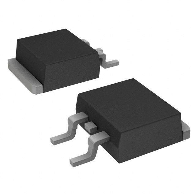
| 产品图片 |
|
| 产品型号 | RJH60D1DPP-M0#T2 |
| rohs | 无铅 / 符合限制有害物质指令(RoHS)规范要求 |
| 产品系列 | - |
| SwitchingEnergy | 100µJ (开), 130µJ (关) |
| TestCondition | 300V, 10A, 5 欧姆, 15V |
| 不同 Vge、Ic时的 Vce(on) | 2.5V @ 15V,10A |
| 供应商器件封装 | TO-220FL |
| 功率-最大值 | 30W |
| 包装 | 管件 |
| 反向恢复时间(trr) | 70ns |
| 安装类型 | 通孔 |
| 封装/外壳 | TO-220-3 整包 |
| 标准包装 | 1 |
| 电压-集射极击穿(最大值) | 600V |
| 电流-集电极(Ic)(最大值) | 20A |
| 输入类型 | 标准 |


- 商务部:美国ITC正式对集成电路等产品启动337调查
- 曝三星4nm工艺存在良率问题 高通将骁龙8 Gen1或转产台积电
- 太阳诱电将投资9.5亿元在常州建新厂生产MLCC 预计2023年完工
- 英特尔发布欧洲新工厂建设计划 深化IDM 2.0 战略
- 台积电先进制程称霸业界 有大客户加持明年业绩稳了
- 达到5530亿美元!SIA预计今年全球半导体销售额将创下新高
- 英特尔拟将自动驾驶子公司Mobileye上市 估值或超500亿美元
- 三星加码芯片和SET,合并消费电子和移动部门,撤换高东真等 CEO
- 三星电子宣布重大人事变动 还合并消费电子和移动部门
- 海关总署:前11个月进口集成电路产品价值2.52万亿元 增长14.8%


PDF Datasheet 数据手册内容提取
Preliminary Datasheet RJH60D1DPP-M0 600V - 10A - IGBT R07DS0158EJ0400 Rev.4.00 Application: Inverter Apr 19, 2012 Features Short circuit withstand time (5 s typ.) Low collector to emitter saturation voltage V = 1.9 V typ. (at I = 10 A, V = 15 V, Ta = 25°C) CE(sat) C GE Built in fast recovery diode (70 ns typ.) in one package Trench gate and thin wafer technology High speed switching t = 75 ns typ. (at V = 300 V, V = 15 V, I = 10 A, Rg = 5 , inductive load) f CC GE C Outline RENESAS Package code: PRSS0003AF-A (Package name: TO-220FL) C 1. Gate 2. Collector G 3. Emitter 1 2 3 E Absolute Maximum Ratings (Ta = 25°C) Item Symbol Ratings Unit Collector to emitter voltage / diode reverse voltage V / V 600 V CES R Gate to emitter voltage V ±30 V GES Collector current Tc = 25°C I 20 A C Tc = 100°C I 10 A C Collector peak current ic(peak) Note1 40 A Collector to emitter diode forward current i 10 A DF Collector to emitter diode forward peak current i (peak) Note1 40 A D Collector dissipation P Note2 30 W C Junction to case thermal resistance (IGBT) j-c Note2 4.1 °C/ W Junction to case thermal resistance (Diode) j-cd Note2 7.2 °C/ W Junction temperature Tj 150 °C Storage temperature Tstg –55 to +150 °C Notes: 1. PW 10 s, duty cycle 1% 2. Value at Tc = 25C R07DS0158EJ0400 Rev.4.00 Page 1 of 9 Apr 19, 2012
RJH60D1DPP-M0 Preliminary Electrical Characteristics (Ta = 25°C) Item Symbol Min Typ Max Unit Test Conditions Collector to emitter breakdown V 600 — — V I =10 A, V = 0 BR(CES) C GE voltage Zero gate voltage collector current I / I — — 5 A V = 600 V, V = 0 CES R CE GE / Diode reverse current Gate to emitter leak current I — — ±1 A V = ±30 V, V = 0 GES GE CE Gate to emitter cutoff voltage V 4.0 — 6.0 V V = 10 V, I = 1 mA GE(off) CE C Collector to emitter saturation voltage V — 1.9 2.5 V I = 10 A, V = 15 V Note3 CE(sat) C GE V — 2.6 — V I = 20 A, V = 15 V Note3 CE(sat) C GE Input capacitance Cies — 275 — pF V = 25 V CE Output capacitance Coes — 25 — pF VGE = 0 Reveres transfer capacitance Cres — 8 — pF f = 1 MHz Total gate charge Qg — 13 — nC V = 15 V GE Gate to emitter charge Qge — 3 — nC VCE = 300 V Gate to collector charge Qgc — 5 — nC IC = 10 A Turn-on delay time t — 30 — ns V = 300 V d(on) CC Rise time tr — 13 — ns VGE = 15 V Turn-off delay time td(off) — 42 — ns IC = 10 A Rg = 5 Fall time t — 75 — ns f (Inductive load) Turn-on energy E — 0.10 — mJ on Turn-off energy E — 0.13 — mJ off Total switching energy E — 0.23 — mJ total Short circuit withstand time t 3.0 5.0 — s V 360 V, V = 15 V sc GE GE FRD forward voltage V — 1.4 1.9 V I = 10 A Note3 F F FRD reverse recovery time t — 70 — ns I = 10 A rr F FRD reverse recovery charge Qrr — 0.11 — C diF/dt = 100 A/s FRD peak reverse recovery current I — 3.5 — A rr Notes: 3. Pulse test. R07DS0158EJ0400 Rev.4.00 Page 2 of 9 Apr 19, 2012
RJH60D1DPP-M0 Preliminary Main Characteristics Collector Dissipation vs. Maximum DC Collector Current vs. Case Temperature Case Temperature 40 30 W) Pc ( 30 (A)C 25 on nt I 20 sipati 20 Curre 15 s ector Di 10 ollector 10 oll C 5 C 0 0 0 25 50 75 100 125 150 175 0 25 50 75 100 125 150 175 Case Temperature Tc (°C) Case Temperature Tc (°C) Maximum Safe Operation Area Turn-off SOA 100 60 A) PW A) 50 ent I (C 10 100 μ = 10 μs ent I (C 40 urr 1 s urr 30 C C ctor ctor 20 olle 0.1 olle C C 10 Tc = 25°C Single pulse 0.01 0 1 10 100 1000 0 200 400 600 800 Collector to Emitter Voltage V (V) Collector to Emitter Voltage V (V) CE CE IGBT Outp ut Characteristics (Typical) IGBT Outp ut Characteristics (Typical) 40 40 Tc = 25°C 18 V Tc = 150°C 18 V 15 V Pulse Test Pulse Test A) A) 15 V (C 30 12 V (C 30 nt I nt I 12 V e e urr 20 10 V urr 20 C C 10 V or or ct ct olle 10 VGE = 8 V olle 10 VGE = 8 V C C 0 0 0 1 2 3 4 5 0 1 2 3 4 5 Collector to Emitter Voltage V (V) Collector to Emitter Voltage V (V) CE CE R07DS0158EJ0400 Rev.4.00 Page 3 of 9 Apr 19, 2012
RJH60D1DPP-M0 Preliminary Collector to Emitter Saturation Voltage Collector to Emitter Saturation Voltage vs. Gate to Emitter Voltage (Typical) vs. Gate to Emitter Voltage (Typical) eV) 5 eV) 5 oltag (at) PTcu l=s e2 5T°eCst oltag (at) on VVCE(s 4 on VVCE(s 4 Collector to Emitter Saturati 1324 8 12 1I6C = 21050 AAA20 Collector to Emitter Saturati 1324 PTcu l=s e1 5T80e°sCt 12 1I6C = 21050 AAA20 Gate to Emitter Voltage V (V) Gate to Emitter Voltage V (V) GE GE Collector to Emitter Saturation Voltage Typical Transfer Characteristics vs. Cas e Temparature (Typical) Collector Current I (A)C 4321000000 VPCuEls e=4 T10e sVtTc8 = 25°C12 11560°C 20 Collector to Emitter Saturation Voltage V (V)CE(sat) 4323211.......0555000−25VPGu0Els e= T1e52s 5Vt 50 75IC 1=0 120500 AAA125 150 Gate to Emitter Voltage VGE (V) Case Temparature Tc (°C) Gate to Emitter Cutoff Voltage vs. Cas e Temparature (Typical) Frequenc y Characteristics (Typical) V) (E(off) 10 A) 5 age VG 8 IC = 10 mA (C(RSM) 4 0 Colle(Scqtoura cruer wreanvt ew)ave utoff Volt 64 urrent I 32 C 1 mA C er or e to Emitt 20 VPCuEls e= T10e sVt Collect 10 TVRjCg =E = =1 5 24 50Ω°0,C Vd, u,T tVcyG ==E 95=00 1°%5C V Gat −25 0 25 50 75 100 125 150 1 10 100 1000 Case Temparature Tc (°C) Frequency f (kHz) R07DS0158EJ0400 Rev.4.00 Page 4 of 9 Apr 19, 2012
RJH60D1DPP-M0 Preliminary Switching Characteristics (Typical) (1) Switching Characteristics (Typical) (2) 1000 10 J) m s) E ( es t (n 100 td(oftff) osses 1 EonEoff m L Ti td(on) y ng erg chi 10 tr En 0.1 wit ng S hi VCC = 300 V, VGE = 15 V wit VCC = 300 V, VGE = 15 V Rg = 5 Ω, Tc = 150°C S Rg = 5 Ω, Tc = 150°C 1 0.01 1 10 100 1 10 100 Collector Current I (A) Collector Current I (A) C C (Inductive load) (Inductive load) Switching Characteristics (Typical) (3) Switching Characteristics (Typical) (4) 1000 1 VCC = 300 V, VGE = 15 V J) s) IC = 10 A, Tc = 150°C E (m e t (n tf sses EEoofnf m o g Ti 100 gy L 0.1 hin td(off) ner witc g E S td(on) hin tr wit VCC = 300 V, VGE = 15 V S IC = 10 A, Tc = 150 °C 10 0.01 1 10 100 1 10 100 Gate Resistance Rg (Ω) Gate Registance Rg (Ω) (Inductive load) (Inductive load) Switching Characteristics (Typical) (5) Switching Characteristics (Typical) (6) 1000 1 VCC = 300 V, VGE = 15 V J) I = 10 A, Rg = 5 Ω m s) C E ( s t (n sses Eon Time 100 tf y Lo 0.1 Eoff ng td(off) erg chi En Swit td(on) tr withing VI C =C1 =0 3A0,0 R Vg, =V 5G EΩ = 15 V S C 10 0.01 25 50 75 100 125 150 25 50 75 100 125 150 Case Temperature Tc (°C) Case Temperature Tc (°C) (Inductive load) (Inductive load) R07DS0158EJ0400 Rev.4.00 Page 5 of 9 Apr 19, 2012
RJH60D1DPP-M0 Preliminary Typical Capacitance vs. Collector to Emitter Voltage Dynamic Input Characteristics (Typical) 1000 V) 800 16 acitance C (pF) 11000 Tc = 25°C CCioeess Emitter Voltage V (CE 640000 VVITCCcCE = C= 1 =20 53 A°0C0 V VGE 182 (V)mitter Voltage VGE Cap VGE = 0 V Cres ector to 200 4 ate to E f = 1 MHz oll G 1 C 0 0 0 50 100 150 200 250 300 0 4 8 12 16 20 Collector to Emitter Voltage V (V) Gate Charge Qg (nc) CE Reverse Recovery Time vs. Reverse Recovery Charge vs. Diode Current Slope (Typical) Diode Current Slope (Typical) 300 C) 0.5 s) VCC = 300 V μ VCC = 300 V me t (nrr 225000 IF = 10 A ge Q (rr 0.4 IF = 10 A Ti har 0.3 y C Recover 110500 Tc = 150°C covery 0.2 Tc = 150°C e e R ers 50 se 0.1 ev 25°C er 25°C R v e 0 R 0 0 40 80 120 160 200 0 40 80 120 160 200 Diode Current Slope diF/dt (A/μs) Diode Current Slope diF/dt (A/μs) Reverse Recovery Current vs. Diode Current Slope (Typical) Forward Current vs. Forward Voltage (Typical) 16 40 A) V = 300 V ent I (rr 12 IFC =C 10 A (A)F 30 Tc = 25°C 150°C Curr nt I ery 8 urre 20 cov Tc = 150°C d C verse Re 4 25°C Forwar 10 VCE = 0 V e Pulse Test R 0 0 0 40 80 120 160 200 0 1 2 3 4 Diode Current Slope diF/dt (A/μs) C-E Diode Forward Voltage VCEF (V) R07DS0158EJ0400 Rev.4.00 Page 6 of 9 Apr 19, 2012
RJH60D1DPP-M0 Preliminary Normalized Transient Thermal Impedance vs. Pulse Width (IGBT) (t)s 10 γe Tc = 25°C c n a d e p m 1 D = 1 al I 0.5 m nt Ther 000..2.015 θθjj –– cc( =t) 4=. 1γs°C (t/)W (cid:129) ,θ Tj c– =c 25°C e 0.1 si PW an 0.02 PDM D = T Tr 0.01 d 1 shot pulse PW e z T ali 0.01 m or 100 μ 1 m 10 m 100 m 1 10 100 N Pulse Width PW (s) Normalized Transient Thermal Impedance vs. Pulse Width (Diode) γ (t)s 10 Tc = 25°C e c n a d e p D = 1 m 1 al I 0.5 m er 0.2 θj – c(t) = γs (t) (cid:129) θj – c Th 0.1 θj – c = 7.2°C/W, Tc = 25°C ent 0.1 0.05 ansi PDM D = PTW d Tr 1 sh0o.00t 1.p0u2lse PW e T z ali 0.01 m 100 μ 1 m 10 m 100 m 1 10 100 or N Pulse Width PW (s) R07DS0158EJ0400 Rev.4.00 Page 7 of 9 Apr 19, 2012
RJH60D1DPP-M0 Preliminary Switching Time Test Circuit Waveform V 90% Diode clamp GE 10% L I C D.U.T V 90% 90% CC Rg 10% 10% td(off) tf td(on) tr Diode Reverse Recovery Time Test Circuit Waveform V CC I F D.U.T I L diF/dt trr F 0 I rr 0.5 I rr Rg 0.9 Irr R07DS0158EJ0400 Rev.4.00 Page 8 of 9 Apr 19, 2012
RJH60D1DPP-M0 Preliminary Package Dimension Package Name JEITA Package Code RENESAS Code Previous Code MASS[Typ.] Unit: mm TO-220FL ⎯ PRSS0003AF-A TO-220FL 1.5g 10.0 ± 0.3 2.8 ± 0.2 0.3 3.0 ± 0.3 ± 6.50.3 ± 0 φ 3.2 ± 0.2 5. 1 3 0. 1.15 ± 0.2 5 ± ± 0. 3.6 1.15 ± 0.2 5 2. 1 0.75 ± 0.15 0.40 ± 0.15 2.54 ± 0.25 2.54 ± 0.25 2 0. ± 5 2 4. 0. ± 6 2. Ordering Information Orderable Part No. Quantity Shipping Container RJH60D1DPP-M0#T2 600 pcs Box (Tube) R07DS0158EJ0400 Rev.4.00 Page 9 of 9 Apr 19, 2012
Notice 1. All information included in this document is current as of the date this document is issued. Such information, however, is subject to change without any prior notice. Before purchasing or using any Renesas Electronics products listed herein, please confirm the latest product information with a Renesas Electronics sales office. Also, please pay regular and careful attention to additional and different information to be disclosed by Renesas Electronics such as that disclosed through our website. 2. Renesas Electronics does not assume any liability for infringement of patents, copyrights, or other intellectual property rights of third parties by or arising from the use of Renesas Electronics products or technical information described in this document. No license, express, implied or otherwise, is granted hereby under any patents, copyrights or other intellectual property rights of Renesas Electronics or others. 3. You should not alter, modify, copy, or otherwise misappropriate any Renesas Electronics product, whether in whole or in part. 4. Descriptions of circuits, software and other related information in this document are provided only to illustrate the operation of semiconductor products and application examples. You are fully responsible for the incorporation of these circuits, software, and information in the design of your equipment. Renesas Electronics assumes no responsibility for any losses incurred by you or third parties arising from the use of these circuits, software, or information. 5. When exporting the products or technology described in this document, you should comply with the applicable export control laws and regulations and follow the procedures required by such laws and regulations. You should not use Renesas Electronics products or the technology described in this document for any purpose relating to military applications or use by the military, including but not limited to the development of weapons of mass destruction. Renesas Electronics products and technology may not be used for or incorporated into any products or systems whose manufacture, use, or sale is prohibited under any applicable domestic or foreign laws or regulations. 6. Renesas Electronics has used reasonable care in preparing the information included in this document, but Renesas Electronics does not warrant that such information is error free. Renesas Electronics assumes no liability whatsoever for any damages incurred by you resulting from errors in or omissions from the information included herein. 7. Renesas Electronics products are classified according to the following three quality grades: "Standard", "High Quality", and "Specific". The recommended applications for each Renesas Electronics product depends on the product's quality grade, as indicated below. You must check the quality grade of each Renesas Electronics product before using it in a particular application. You may not use any Renesas Electronics product for any application categorized as "Specific" without the prior written consent of Renesas Electronics. Further, you may not use any Renesas Electronics product for any application for which it is not intended without the prior written consent of Renesas Electronics. Renesas Electronics shall not be in any way liable for any damages or losses incurred by you or third parties arising from the use of any Renesas Electronics product for an application categorized as "Specific" or for which the product is not intended where you have failed to obtain the prior written consent of Renesas Electronics. The quality grade of each Renesas Electronics product is "Standard" unless otherwise expressly specified in a Renesas Electronics data sheets or data books, etc. "Standard": Computers; office equipment; communications equipment; test and measurement equipment; audio and visual equipment; home electronic appliances; machine tools; personal electronic equipment; and industrial robots. "High Quality": Transportation equipment (automobiles, trains, ships, etc.); traffic control systems; anti-disaster systems; anti-crime systems; safety equipment; and medical equipment not specifically designed for life support. "Specific": Aircraft; aerospace equipment; submersible repeaters; nuclear reactor control systems; medical equipment or systems for life support (e.g. artificial life support devices or systems), surgical implantations, or healthcare intervention (e.g. excision, etc.), and any other applications or purposes that pose a direct threat to human life. 8. You should use the Renesas Electronics products described in this document within the range specified by Renesas Electronics, especially with respect to the maximum rating, operating supply voltage range, movement power voltage range, heat radiation characteristics, installation and other product characteristics. Renesas Electronics shall have no liability for malfunctions or damages arising out of the use of Renesas Electronics products beyond such specified ranges. 9. Although Renesas Electronics endeavors to improve the quality and reliability of its products, semiconductor products have specific characteristics such as the occurrence of failure at a certain rate and malfunctions under certain use conditions. Further, Renesas Electronics products are not subject to radiation resistance design. Please be sure to implement safety measures to guard them against the possibility of physical injury, and injury or damage caused by fire in the event of the failure of a Renesas Electronics product, such as safety design for hardware and software including but not limited to redundancy, fire control and malfunction prevention, appropriate treatment for aging degradation or any other appropriate measures. Because the evaluation of microcomputer software alone is very difficult, please evaluate the safety of the final products or system manufactured by you. 10. Please contact a Renesas Electronics sales office for details as to environmental matters such as the environmental compatibility of each Renesas Electronics product. Please use Renesas Electronics products in compliance with all applicable laws and regulations that regulate the inclusion or use of controlled substances, including without limitation, the EU RoHS Directive. Renesas Electronics assumes no liability for damages or losses occurring as a result of your noncompliance with applicable laws and regulations. 11. This document may not be reproduced or duplicated, in any form, in whole or in part, without prior written consent of Renesas Electronics. 12. Please contact a Renesas Electronics sales office if you have any questions regarding the information contained in this document or Renesas Electronics products, or if you have any other inquiries. (Note 1) "Renesas Electronics" as used in this document means Renesas Electronics Corporation and also includes its majority-owned subsidiaries. (Note 2) "Renesas Electronics product(s)" means any product developed or manufactured by or for Renesas Electronics. SALES OFFICES http://www.renesas.com Refer to "http://www.renesas.com/" for the latest and detailed information. Renesas Electronics America Inc. 2880 Scott Boulevard Santa Clara, CA 95050-2554, U.S.A. Tel: +1-408-588-6000, Fax: +1-408-588-6130 Renesas Electronics Canada Limited 1101 Nicholson Road, Newmarket, Ontario L3Y 9C3, Canada Tel: +1-905-898-5441, Fax: +1-905-898-3220 Renesas Electronics Europe Limited Dukes Meadow, Millboard Road, Bourne End, Buckinghamshire, SL8 5FH, U.K Tel: +44-1628-585-100, Fax: +44-1628-585-900 Renesas Electronics Europe GmbH Arcadiastrasse 10, 40472 Düsseldorf, Germany Tel: +49-211-65030, Fax: +49-211-6503-1327 Renesas Electronics (China) Co., Ltd. 7th Floor, Quantum Plaza, No.27 ZhiChunLu Haidian District, Beijing 100083, P.R.China Tel: +86-10-8235-1155, Fax: +86-10-8235-7679 Renesas Electronics (Shanghai) Co., Ltd. Unit 204, 205, AZIA Center, No.1233 Lujiazui Ring Rd., Pudong District, Shanghai 200120, China Tel: +86-21-5877-1818, Fax: +86-21-6887-7858 / -7898 Renesas Electronics Hong Kong Limited Unit 1601-1613, 16/F., Tower 2, Grand Century Place, 193 Prince Edward Road West, Mongkok, Kowloon, Hong Kong Tel: +852-2886-9318, Fax: +852 2886-9022/9044 Renesas Electronics Taiwan Co., Ltd. 13F, No. 363, Fu Shing North Road, Taipei, Taiwan Tel: +886-2-8175-9600, Fax: +886 2-8175-9670 Renesas Electronics Singapore Pte. Ltd. 1 harbourFront Avenue, #06-10, keppel Bay Tower, Singapore 098632 Tel: +65-6213-0200, Fax: +65-6278-8001 Renesas Electronics Malaysia Sdn.Bhd. Unit 906, Block B, Menara Amcorp, Amcorp Trade Centre, No. 18, Jln Persiaran Barat, 46050 Petaling Jaya, Selangor Darul Ehsan, Malaysia Tel: +60-3-7955-9390, Fax: +60-3-7955-9510 Renesas Electronics Korea Co., Ltd. 11F., Samik Lavied' or Bldg., 720-2 Yeoksam-Dong, Kangnam-Ku, Seoul 135-080, Korea Tel: +82-2-558-3737, Fax: +82-2-558-5141 © 2012 Renesas Electronics Corporation. All rights reserved. Colophon 1.1