ICGOO在线商城 > 集成电路(IC) > PMIC - 稳压器 - 线性 > REG1117-5
 Datasheet下载
- 型号: REG1117-5
- 制造商: Texas Instruments
- 库位|库存: xxxx|xxxx
- 要求:
| 数量阶梯 | 香港交货 | 国内含税 |
| +xxxx | $xxxx | ¥xxxx |
查看当月历史价格
查看今年历史价格
REG1117-5产品简介:
ICGOO电子元器件商城为您提供REG1117-5由Texas Instruments设计生产,在icgoo商城现货销售,并且可以通过原厂、代理商等渠道进行代购。 REG1117-5价格参考¥1.08-¥1.08。Texas InstrumentsREG1117-5封装/规格:PMIC - 稳压器 - 线性, Linear Voltage Regulator IC Positive Fixed 1 Output 5V 800mA SOT-223-4。您可以下载REG1117-5参考资料、Datasheet数据手册功能说明书,资料中有REG1117-5 详细功能的应用电路图电压和使用方法及教程。
| 参数 | 数值 |
| 产品目录 | 集成电路 (IC)半导体 |
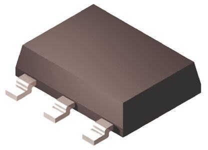
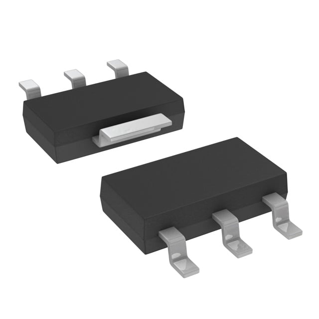
| 描述 | IC REG LDO 5V 0.8A SOT223低压差稳压器 800mA & 1A LDO |
| 产品分类 | |
| 品牌 | Texas Instruments |
| 产品手册 | |
| 产品图片 |
|
| rohs | 符合RoHS无铅 / 符合限制有害物质指令(RoHS)规范要求 |
| 产品系列 | 电源管理 IC,低压差稳压器,Texas Instruments REG1117-5- |
| 数据手册 | |
| 产品型号 | REG1117-5 |
| 产品目录页面 | |
| 产品种类 | 低压差稳压器 |
| 供应商器件封装 | SOT-223 |
| 其它名称 | REG11175 |
| 包装 | 管件 |
| 商标 | Texas Instruments |
| 回动电压—最大值 | 1.1 V at 100 mA |
| 安装类型 | 表面贴装 |
| 安装风格 | SMD/SMT |
| 封装 | Tube |
| 封装/外壳 | TO-261-4,TO-261AA |
| 封装/箱体 | SOT-223-4 |
| 工作温度 | -40°C ~ 125°C |
| 工厂包装数量 | 80 |
| 最大工作温度 | + 125 C |
| 最大输入电压 | 15 V |
| 最小工作温度 | - 40 C |
| 最小输入电压 | + 3.8 V |
| 标准包装 | 80 |
| 电压-跌落(典型值) | 1.1V @ 800mA |
| 电压-输入 | 最高 15V |
| 电压-输出 | 5V |
| 电压调节准确度 | 1 % |
| 电流-输出 | 800mA |
| 电流-限制(最小值) | 800mA |
| 稳压器拓扑 | 正,固定式 |
| 稳压器数 | 1 |
| 系列 | REG1117-5 |
| 线路调整率 | 10 mV |
| 负载调节 | 15 mV |
| 输入偏压电流—最大 | 4 mA |
| 输出电压 | 5 V |
| 输出电流 | 800 mA |
| 输出端数量 | 1 Output |
| 输出类型 | Fixed |


- 商务部:美国ITC正式对集成电路等产品启动337调查
- 曝三星4nm工艺存在良率问题 高通将骁龙8 Gen1或转产台积电
- 太阳诱电将投资9.5亿元在常州建新厂生产MLCC 预计2023年完工
- 英特尔发布欧洲新工厂建设计划 深化IDM 2.0 战略
- 台积电先进制程称霸业界 有大客户加持明年业绩稳了
- 达到5530亿美元!SIA预计今年全球半导体销售额将创下新高
- 英特尔拟将自动驾驶子公司Mobileye上市 估值或超500亿美元
- 三星加码芯片和SET,合并消费电子和移动部门,撤换高东真等 CEO
- 三星电子宣布重大人事变动 还合并消费电子和移动部门
- 海关总署:前11个月进口集成电路产品价值2.52万亿元 增长14.8%


PDF Datasheet 数据手册内容提取
REG1117 REG1117A SBVS001D − OCTOBER 1992 − REVISED JULY 2004 800mA and 1A Low Dropout Positive Regulator 1.8V, 2.5V, 2.85, 3.3V, 5V, and Adjustable FEATURES DESCRIPTION (cid:1) FIXED AND ADJUSTABLE VERSIONS The REG1117 is a family of easy-to-use three-terminal (cid:1) 2.85V MODEL FOR SCSI-2 ACTIVE voltage regulators. The family includes a variety of fixed- TERMINATION and adjustable-voltage versions, two currents (800mA and (cid:1) 1A) and two package types (SOT-223 and DDPAK). See OUTPUT CURRENT: the chart below for available options. REG1117: 800mA max REG1117A: 1A max Output voltage of the adjustable versions is set with two (cid:1) OUTPUT TOLERANCE: (cid:1)1% max external resistors. The REG1117 low dropout voltage (cid:1) allows its use with as little as 1V input-output voltage DROPOUT VOLTAGE: differential. REG1117: 1.2V max at I = 800mA O REG1117A: 1.3V max at I = 1A Laser trimming assures excellent output voltage accuracy O (cid:1) without adjustment. An NPN output stage allows output INTERNAL CURRENT LIMIT (cid:1) stage drive to contribute to the load current for maximum THERMAL OVERLOAD PROTECTION efficiency. (cid:1) SOT-223 AND DDPAK SURFACE-MOUNT PACKAGES 800mA 1A VOLTAGE SOT-223 DDPAK SOT-223 DDPAK APPLICATIONS 1.8V (cid:2) (cid:2) (cid:1) SCSI-2 ACTIVE TERMINATION 2.5V (cid:2) (cid:2) (cid:1) HAND-HELD DATA COLLECTION DEVICES 2.85V (cid:2) (cid:1) HIGH EFFICIENCY LINEAR REGULATORS 3.3V (cid:2) (cid:2) (cid:1) BATTERY-POWERED INSTRUMENTATION 5V (cid:2) (cid:2) (cid:1) BATTERY MANAGEMENT CIRCUITS FOR Adjustable (cid:2) (cid:2) (cid:2) NOTEBOOK AND PALMTOP PCs (cid:1) CORE VOLTAGE SUPPLY: FPGA, PLD, DSP, CPU Please be aware that an important notice concerning availability, standard warranty, and use in critical applications of TexasInstruments semiconductor products and disclaimers thereto appears at the end of this data sheet. All trademarks are the property of their respective owners. (cid:1)(cid:2)(cid:3)(cid:4)(cid:5)(cid:6)(cid:7)(cid:8)(cid:3)(cid:9) (cid:4)(cid:10)(cid:7)(cid:10) (cid:11)(cid:12)(cid:13)(cid:14)(cid:15)(cid:16)(cid:17)(cid:18)(cid:11)(cid:14)(cid:12) (cid:11)(cid:19) (cid:20)(cid:21)(cid:15)(cid:15)(cid:22)(cid:12)(cid:18) (cid:17)(cid:19) (cid:14)(cid:13) (cid:23)(cid:21)(cid:24)(cid:25)(cid:11)(cid:20)(cid:17)(cid:18)(cid:11)(cid:14)(cid:12) (cid:26)(cid:17)(cid:18)(cid:22)(cid:27) (cid:1)(cid:15)(cid:14)(cid:26)(cid:21)(cid:20)(cid:18)(cid:19) Copyright 1992−2004, Texas Instruments Incorporated (cid:20)(cid:14)(cid:12)(cid:13)(cid:14)(cid:15)(cid:16) (cid:18)(cid:14) (cid:19)(cid:23)(cid:22)(cid:20)(cid:11)(cid:13)(cid:11)(cid:20)(cid:17)(cid:18)(cid:11)(cid:14)(cid:12)(cid:19) (cid:23)(cid:22)(cid:15) (cid:18)(cid:28)(cid:22) (cid:18)(cid:22)(cid:15)(cid:16)(cid:19) (cid:14)(cid:13) (cid:7)(cid:22)(cid:29)(cid:17)(cid:19) (cid:8)(cid:12)(cid:19)(cid:18)(cid:15)(cid:21)(cid:16)(cid:22)(cid:12)(cid:18)(cid:19) (cid:19)(cid:18)(cid:17)(cid:12)(cid:26)(cid:17)(cid:15)(cid:26) (cid:30)(cid:17)(cid:15)(cid:15)(cid:17)(cid:12)(cid:18)(cid:31)(cid:27) (cid:1)(cid:15)(cid:14)(cid:26)(cid:21)(cid:20)(cid:18)(cid:11)(cid:14)(cid:12) (cid:23)(cid:15)(cid:14)(cid:20)(cid:22)(cid:19)(cid:19)(cid:11)(cid:12)! (cid:26)(cid:14)(cid:22)(cid:19) (cid:12)(cid:14)(cid:18) (cid:12)(cid:22)(cid:20)(cid:22)(cid:19)(cid:19)(cid:17)(cid:15)(cid:11)(cid:25)(cid:31) (cid:11)(cid:12)(cid:20)(cid:25)(cid:21)(cid:26)(cid:22) (cid:18)(cid:22)(cid:19)(cid:18)(cid:11)(cid:12)! (cid:14)(cid:13) (cid:17)(cid:25)(cid:25) (cid:23)(cid:17)(cid:15)(cid:17)(cid:16)(cid:22)(cid:18)(cid:22)(cid:15)(cid:19)(cid:27) www.ti.com
(cid:2)"#$$$% (cid:2)"#$$$%(cid:10) www.ti.com SBVS001D − OCTOBER 1992 − REVISED JULY 2004 ABSOLUTE MAXIMUM RATINGS(1) This integrated circuit can be damaged by ESD. Texas Instruments recommends that all integrated circuits be Power Dissipation. . . . . . . . . . . . . . . . . . . . . . . . . . Internally Limited handled with appropriate precautions. Failure to observe Input Voltage. . . . . . . . . . . . . . . . . . . . . . . . . . . . . . . . . . . . . . . +15V proper handling and installation procedures can cause damage. Operating Junction Temperature Range. . . . . . . . −40°C to +125°C ESD damage can range from subtle performance degradation to Storage Temperature Range . . . . . . . . . . . . . . . . . −65°C to +150°C complete device failure. Precision integrated circuits may be more Lead Temperature (soldering, 10s)(2) . . . . . . . . . . . . . . . . . +300°C susceptible to damage because very small parametric changes could cause the device not to meet its published specifications. (1)Stresses above these ratings may cause permanent damage. (2)See Soldering Methods section. CONNECTION DIAGRAM Front View PlasticDDPAK PlasticSOT−223 Tabis V OUT TabisV OUT Ground V V Ground V V OUT IN OUT IN (Adj.)(1) (Adj.)(1) NOTE:(1)Adjustable−VoltageModel. 2
(cid:2)"#$$$% (cid:2)"#$$$%(cid:10) www.ti.com SBVS001D − OCTOBER 1992 − REVISED JULY 2004 PACKAGE/ORDERING INFORMATION(1) OPERATING TRANSPORT PACKAGE PACKAGE ORDERING PRODUCT VO/IO PACKAGE-LEAD DESIGNATOR TEMPERATURE MARKING NUMBER MEDIA, RANGE QUANTITY REG1117-2.85 Rails, 80 −−4400°°CC ttoo REG1117-2.85 2.85/800mA SOT223-3 DCY +125°C BB11172 REG1117-2.85 Tape and Reel, 2500 REG1117-3.3 Rails, 80 −−4400°°CC ttoo REG1117-3.3 3.3/800mA SOT223-3 DCY +125°C BB11174 REG1117-3.3 Tape and Reel, 2500 Tape and Reel, REG1117F-3.3KTTT −−4400°CC ttoo 50 RREEGG11111177FF--33..33 33..33//880000mmAA DDDDPPAAKK--33 KKTTTT BBBB11111177FF44 +125°C Tape and Reel, REG1117F-3.3/500 500 REG1117-5 Rails, 80 −−4400°°CC ttoo REG1117-5 5V/800mA SOT223-3 DCY +125°C BB11175 REG1117-5 Tape and Reel, 2500 REG1117 Rails, 80 −−4400°°CC ttoo REG1117 Adj./800mA SOT223-3 DCY +125°C BB1117 REG1117 Tape and Reel, 2500 REG1117A-1.8 Rails, 80 −−4400°°CC ttoo REG1117A-1.8 1.8V/1A SOT223-3 DCY +125°C R111718 REG1117A-1.8 Tape and Reel, 2500 Tape and Reel, REG1117FA-1.8KTTT −−4400°CC ttoo 50 RREEGG11111177FFAA--11..88 11..88//11AA DDDDPPAAKK--33 KKTTTT RREEGG11111177FFAA11..88 +125°C Tape and Reel, REG1117FA-1.8/500 500 REG1117A-2.5 Rails, 80 −−4400°°CC ttoo REG1117A-2.5 2.5/1A SOT223-3 DCY +125°C R111725 REG1117A-2.5 Tape and Reel, 2500 Tape and Reel, REG1117FA-2.5KTTT −−4400°CC ttoo 50 RREEGG11111177FFAA--22..55 22..55//11AA DDDDPPAAKK--33 KKTTTT RREEGG11111177FFAA22..55 +125°C Tape and Reel, REG1117FA-2.5/500 500 Tape and Reel, REG1117FA-5/KTTT −−4400°CC ttoo 50 RREEGG11111177FFAA--55 55//11AA DDDDPPAAKK--33 KKTTTT BBBB11111177FFAA55..00 +125°C Tape and Reel, REG1117FA-5/500 500 REG1117A Rails, 80 −−4400°°CC ttoo REG1117A Adj./1A SOT223-3 DCY +125°C BB1117A REG1117A Tape and Reel, 2500 Tape and Reel, REG1117FA/KTTT −−4400°CC ttoo 50 RREEGG11111177FFAA AAddjj..//11AA DDDDPPAAKK--33 KKTTTT RREEGG11111177FFAA +125°C Tape and Reel, REG1117FA/500 500 (1)For the most current package and ordering information, see the Package Option Addendum located at the end of this data sheet. 3
(cid:2)"#$$$% (cid:2)"#$$$%(cid:10) www.ti.com SBVS001D − OCTOBER 1992 − REVISED JULY 2004 ELECTRICAL CHARACTERISTICS At TJ = +25°C, unless otherwise noted. REG1117, REG1117A PARAMETER CONDITION MIN TYP MAX UNIT OUTPUT VOLTAGE REG1117-2.85 I = 10mA, V = 4.85V 2.820 2.85 2.880 V O IN See Note 1 I = 0 to 800mA, V = 4.05V to 10V 2.790 2.85 2.910 V O IN REG1117-3.3 I = 10mA, V = 5.3V 3.270 3.30 3.330 V O IN See Note 1 I = 0 to 800mA, V = 4.8V to 10V 3.240 3.30 3.360 V O IN REG1117-5 I = 10mA, V = 7V 4.950 5.00 5.050 V O IN See Note 1 I = 0 to 800mA, V = 6.5V to 10V 4.900 5.00 5.100 V O IN REG1117A-1.8 I = 10mA, V = 3.8V 1.782 1.8 1.818 V O IN See Note 1 I = 0 to 1A, V = 3.8V to 10V 1.764 1.8 1.836 V O IN REG1117A-2.5 I = 10mA, V = 4.5V 2.475 2.5 2.525 V O IN See Note 1 I = 0 to 1A, V = 4.5V to 10V 2.450 2.5 2.550 V O IN REG1117A-5 I = 10mA, V = 7V 4.950 5.0 5.050 V O IN See Note 1 I = 0 to 1A, V = 7V to 10V 4.900 5.0 5.100 V O IN REFERENCE VOLTAGE REG1117 (Adjustable) I = 10mA, V − V = 2V 1.238 1.250 1.262 V O IN O See Note 1 I = 10 to 800mA, V − V = 1.4 to 10V 1.225 1.250 1.280 V O IN O REG1117A (Adjustable) I = 10mA, V − V = 2V 1.238 1.250 1.262 V O IN O See Note 1 I = 10mA to 1A, V − V = 1.4 to 10V 1.225 1.250 1.280 V O IN O LINE REGULATION REG1117-2.85(1) I = 0, V = 4.25 to 10V 1 7 mV O IN REG1117-3.3(1) I = 0, V = 4.8 to 10V 2 7 mV O IN REG1117-5(1) I = 0, V = 6.5 to 15V 3 10 mV O IN REG1117 (Adjustable)(1) IO = 10mA, VIN − VO = 1.5 to 13.75V 0.1 0.4 % REG1117A (Adjustable)(1) IO = 10mA, VIN − VO = 1.5 to 13.75V 0.1 0.4 % REG1117A-1.8(1) I = 0, V = 3.8V to 10V 1 7 mV O IN REG1117A-2.5(1) I = 0, V = 4.5V to 10V 1 7 mV O IN REG1117A-5.0(1) I = 0, V = 7V to 15V 3 10 mV O IN LOAD REGULATION REG1117-2.85(1) I = 0 to 800mA, V = 4.25V 2 10 mV O IN REG1117-3.3(1) I = 0 to 800mA, V = 4.8V 3 12 mV O IN REG1117-5(1) I = 0 to 800mA, V = 6.5V 3 15 mV O IN REG1117 (Adjustable)(1)(2) I = 10 to 800mA, V − V = 3V 0.1 0.4 % O IN O REG1117A (Adjustable)(1)(2) IO = 10mA to 1A, VIN − VO = 3V 0.1 0.4 % REG1117A-1.8(1) I = 0 to 1A, V = 3.8V 2 10 mV O IN REG1117A-2.5 I = 0 to 1A, V = 4.5V 2 10 mV O IN REG1117A-5 I = 0 to 1A, V = 7.0V 3 15 mV O IN DROPOUT VOLTAGE(3) All Models(1) I = 100mA 1.00 1.10 V O See Note 1 I = 500mA 1.05 1.15 V O REG1117 Models(1) I = 800mA 1.10 1.20 V O REG1117A I = 1A 1.2 1.30 V O See Note 1 I = 1A 1.2 1.55 V O (1)Specification applies over the full specified junction temperature range, 0°C to +125°C. (2)REG1117 and REG1117A adjustable versions require a minimum load current for ±3% regulation. (3)Dropout voltage is the input voltage minus output voltage that produces a 1% decrease in output voltage. (4)Percentage change in unloaded output voltage before versus after a 30ms power pulse of IO = 800mA (REG1117 models), IO = 1A (REG1117A), VIN − VO = 1.4V (reading taken 10ms after pulse). 4
(cid:2)"#$$$% (cid:2)"#$$$%(cid:10) www.ti.com SBVS001D − OCTOBER 1992 − REVISED JULY 2004 ELECTRICAL CHARACTERISTICS (continued) At TJ = +25°C, unless otherwise noted. REG1117, REG1117A PARAMETER CONDITION MIN TYP MAX UNIT CURRENT LIMIT REG1117 Models V − V = 5V 800 950 1200 mA IN O REG1117A V − V = 5V 1000 1250 1600 mA IN O MINIMUM LOAD CURRENT Adjustable Models(1)(2) V − V = 13.75V 1.7 5 mA IN O QUIESCENT CURRENT Fixed-Voltage Models(1) V − V = 5V 4 10 mA IN O ADJUSTABLE PIN CURRENT(1)(2) I = 10mA, V − V = 1.4 to 10V 50 120 µA O IN O vs Load Current, REG1117(1) I = 10mA to 800mA, V − V = 1.4 to 10V 0.5 5 µA O IN O vs Load Current, REG1117A(1) I = 10mA to 1A, V − V = 1.4 to 10V 0.5 5 µA O IN O THERMAL REGULATION All Models(4) 30ms Pulse 0.01 0.1 %/W RIPPLE REJECTION All Models f = 120Hz, VIN − VOUT = 3V + 1VPP Ripple 62 dB TEMPERATURE DRIFT Fixed-Voltage Models T = 0°Cto +125°C 0.5 % J Adjustable Models T = 0°Cto +125°C 2 % J LONG-TERM STABILITY All Models TA = 125°C, 1000Hr 0.3 % OUTPUT NOISE rms Noise, All Models f = 10Hz to 10kHz 0.003 % THERMAL RESISTANCE Thermal Resistance, (cid:1)JC (Junction-to-Case at Tab) 3-Lead SOT-223 Surface-Mount 15 °C/W 3-Lead DDPAK Surface-Mount f > 50Hz 2 °C/W dc 3 °C/W Thermal Resistance, (cid:1)JA (Junction-to-Case at Tab) 3-Lead DDPAK Surface-Mount No Heatsink 65 °C/W (1)Specification applies over the full specified junction temperature range, 0°C to +125°C. (2)REG1117 and REG1117A adjustable versions require a minimum load current for ±3% regulation. (3)Dropout voltage is the input voltage minus output voltage that produces a 1% decrease in output voltage. (4)Percentage change in unloaded output voltage before versus after a 30ms power pulse of IO = 800mA (REG1117 models), IO = 1A (REG1117A), VIN − VO = 1.4V (reading taken 10ms after pulse). 5
(cid:2)"#$$$% (cid:2)"#$$$%(cid:10) www.ti.com SBVS001D − OCTOBER 1992 − REVISED JULY 2004 SIMPLIFIED SCHEMATIC V IN + Current Limit Thermal Limit V 10X OUT (Substrate) Ground(Fixed−voltageModels) Adj.(Adjustable−voltageModel) 6
(cid:2)"#$$$% (cid:2)"#$$$%(cid:10) www.ti.com SBVS001D − OCTOBER 1992 − REVISED JULY 2004 TYPICAL CHARACTERISTICS At TA = +25°C, all models, unless otherwise noted. LOADREGULATION SHORT−CIRCUITCURRENTvsTEMPERATURE (∆I =800mA) LOAD 1400 1 0 1300 V) REG1117−2.85 A) m m ( 1 Current( 11210000 REG1117A Deviation −−23 REG1117A−1.8 uit ge Circ 1000 REG1117Models olta −4 − V ort ut −5 Sh 900 utp REG1117−5 O −6 800 −7 −50 −25 0 25 50 75 100 −50 −25 0 25 50 75 100 Temperature((cid:3)C) Temperature((cid:3)C) LINEREGULATIONvsTEMPERATURE RIPPLEREJECTIONvsFREQUENCY 6 100 5 90 IOUT=100mA V) VIN=6.5Vto15V 80 VRIPPLE=1.0VPP e(m 4 REG1117−5 dB) 70 g ( an 3 on 60 Ch 2 ecti 50 utVoltage 10 REG1117A−1.8 RippleRej 4300 utp VIN=3.8Vto10V 20 O −1 10 −2 0 −50 −25 0 25 50 75 100 10 100 1k 10k 100k Temperature((cid:3)C) Frequency(Hz) OUTPUTVOLTAGEvsTEMPERATURE QUIESCENTCURRENTvsTEMPERATURE 2.0 8 IO=10mA 7 %) Fixed−VoltageModels ( 1.0 A) 6 e m ang nt( 5 h e geC 0 Curr 4 Volta scent 3 utput −1.0 Quie 2 O 1 −2.0 0 −50 −25 0 25 50 75 100 −50 −25 0 25 50 75 100 Temperature((cid:3)C) Temperature((cid:3)C) 7
(cid:2)"#$$$% (cid:2)"#$$$%(cid:10) www.ti.com SBVS001D − OCTOBER 1992 − REVISED JULY 2004 TYPICAL CHARACTERISTICS (continued) At TA = +25°C, all models, unless otherwise noted. LOADTRANSIENTRESPONSE LINETRANSIENTRESPONSE 60 OutputVoltageDeviations(V)−00..101 OutputVoltageDeviation(mV) 42000 CCIOIOUNUT=T==10µ1.F10AµFTantalum −20 A) 0.5 CCIONU=T=101µ0FµF V) −40 Current( −0.05 PTVaIrNenl=toaa4lud.2m=5V0.1A Voltage( 54..2255 Load 0 20 40 60 80 100 Input 3.25 0 20 40 60 80 100 120 140 160 180 200 Time(µs) Time(µs) APPLICATIONS INFORMATION Figure 2 shows a hookup diagram for the adjustable voltage model. Resistor values are shown for some Figure 1 shows the basic hookup diagram for fixed-voltage commonly-used output voltages. Values for other voltages models. All models require an output capacitor for proper can be calculated from the equation shown in Figure 2. For operation, and for improving high-frequency load best load regulation, connect R close to the output pin and 1 regulation; a 10µF tantalum capacitor is recommended. R close to the ground side of the load as shown. 2 Aluminum electrolytic types of 50µF or greater can also be used. A high-quality capacitor should be used to assure that the ESR (Effective Series Resistance) is less than THERMAL CONSIDERATIONS 0.5Ω. The REG1117 has current limit and thermal shutdown circuits that protect it from overload. The thermal shutdown activates at approximately TJ = 165°C. For continuous operation, however, the junction temperature should not be allowed to exceed 125°C. Any tendency to activate the thermal shutdown in normal use is an indication of an VIN REG1117 VO inadequate heat sink or excessive power dissipation. The 10µF + +10µF power dissipation is equal to: Tantalum Tantalum P = (V – V ) I D IN OUT OUT The junction temperature can be calculated by: T = T + P ((cid:1) ) J A D JA Figure 1. Fixed-Voltage Model—Basic where TA is the ambient temperature, and (cid:1)JA is the Connections junction-to-ambient thermal resistance. VIN 3 REG1117 2 VO V R R (Adj) (OVU)T (Ω)(12) (Ω)(22) 10µCF1+ 1 R1 +C102µF Load VO= R1R+1R2 x(1.25V)+(50µA)(R2) 11.2.55 O7p5e0n S1h4o7rt 2.1 158 107 C(1)+ 2.85 169 215 103µF R2 Thistermisnegligiblewith 3 137 191 properchoiceofvalues−see 3.3 115 187 tableatright. 5 113 340 10 113 787 NOTES:(1)C optional.Improveshigh−frequencylinerejection.(2)Resistorsarestandard1%values. 3 Figure 2. Adjustable-Voltage Model—Basic Connections 8
(cid:2)"#$$$% (cid:2)"#$$$%(cid:10) www.ti.com SBVS001D − OCTOBER 1992 − REVISED JULY 2004 A simple experiment will determine whether the maximum LAYOUT CONSIDERATIONS recommended junction temperature is exceeded in an The DDPAK (REG1117F-3.3 and REG1117FA) is a actual circuit board and mounting configuration: Increase surface-mount power package that has excellent thermal the ambient temperature above that expected in normal characteristics. For best thermal performance, the operation until the device’s thermal shutdown is activated. mounting tab should be soldered directly to a circuit board If this occurs at more than 40°C above the maximum copper area, as shown in Figure 3. Increasing the copper expected ambient temperature, then TJ will be less than area improves heat dissipation. Figure 4 shows typical 125°C during normal operation. thermal resistance from junction-to-ambient as a function The internal protection circuitry of the REG1117 was of the copper area. designed to protect against overload conditions. It was not intended to replace proper heat sinking. Continuously running the REG1117 into thermal shutdown will degrade reliability. 3−LeadDDPAK(1) 0.51 5 4 0. 5 8 0 0. 2 Allmeasurements 0. ininches. 0.155 0.05 0.10 NOTE:(1)Forimprovedthermalperformanceincrease footprintarea.SeeFigure4(ThermalResistancevs CircuitBoardCopperArea). Figure 3. DDPAK Footprint THERMALRESISTANCEvs CIRCUITBOARDCOPPERAREA CircuitBoardCopperArea 60 W) REG1117F C/ 50 DDPAKSurfaceMountPackage ° (A 1ozcopper (cid:1)J e, 40 c n a st si 30 e R al m er 20 h T REG1117F DDPAKSurface−MountPackage 10 0 1 2 3 4 5 CopperArea(inches2) Figure 4. DDPAK Thermal Resistance versus Circuit Board Copper Area 9
(cid:2)"#$$$% (cid:2)"#$$$%(cid:10) www.ti.com SBVS001D − OCTOBER 1992 − REVISED JULY 2004 The SOT-223 package derives heat sinking from Table 1. SOT-223 (cid:1) for Various Board JA conduction through its copper leads, especially the large Configurations mounting tab. These must be soldered to a circuit board with a substantial amount of copper remaining, as shown SOT-223 in Figure 5. Circuit board traces connecting the tab and the TTHHEERRMMAALL TOTAL PC TOPSIDE((11)) BACKSIDE RESISTANCE leads should be made as large as practical. The mounting BBOOAARRDD CCOOPPPPEERR CCOOPPPPEERR JJUUNNCCTTIIOONN-- tab of both packages is electrically connected to V . OUT AREA AREA AREA TO-AMBIENT 2500mm2 2500mm2 2500mm2 46°C/W 2500mm2 1250mm2 2500mm2 47°C/W TotalArea:50x50mm 2500mm2 950mm2 2500mm2 49°C/W 2500mm2 2500mm2 0 51°C/W 2500mm2 1800mm2 0 53°C/W 35x17mm 1600mm2 600mm2 1600mm2 55°C/W 2500mm2 1250mm2 0 58°C/W 2500mm2 915mm2 0 59°C/W 16x10mm 16x10mm 1600mm2 600mm2 0 67°C/W 900mm2 340mm2 900mm2 72°C/W 900mm2 340mm2 0 85°C/W Withoutbacksidecopper:(cid:1) ≈59(cid:3)C/W JA Withsolidbacksidecopper:(cid:1)JA≈49(cid:3)C/W (1)Tab is attached to the topside copper. Figure 5. SOT-223 Circuit Board Layout Example SOLDERING METHODS Other nearby circuit traces, including those on the back Both REG1117 packages are suitable for infrared reflow side of the circuit board, help conduct heat away from the and vapor-phase reflow soldering techniques. The high device, even though they may not be electrically rate of temperature change that occurs with wave connected. Make all nearby copper traces as wide as soldering or hand soldering can damage the REG1117. possible and leave only narrow gaps between traces. Table 1 shows approximate values of (cid:1) for various circuit INSPEC Abstract Number: B91007604, C91012627. JA board and copper areas for the SOT-223 package. Nearby Kelly, E.G. “Thermal Characteristics of Surface 5WK9Ω heat dissipating components, circuit board mounting Packages.” The Proceedings of SMTCON. Surface Mount conditions, and ventilation can dramatically affect the Technology Conference and Exposition: Competitive actual (cid:1) . Proper heat sinking significantly increases the Surface Mount Technology, April 3−6, 1990, Atlantic City, JA maximum power dissipation at a given ambient NJ, USA. Abstract Publisher: IC Manage, 1990, Chicago, temperature, as shown in Figure 6. IL, USA. MAXIMUMPOWERDISSIPATION vsAMBIENTTEMPERATURE 6 (cid:1)(4JAin2=o2n7e(cid:3)oCz/Wcopper PD=T(T(mJ(amxa)x=)1−5T0A(cid:3))C/(cid:1)JA 5 mountingpad) J s) att n(W 4 ((cid:1)2JA50=04m6m(cid:3)2Ct/oWpsideand DSODPT−A2K23 patio 3 backsidecopper) Dissi (cid:1)JA=65(cid:3)(nCo/Wheatsink) er 2 w Po 1 (cid:1)JA=85(cid:3)C/W (340mm2topsidecopper, nobacksidecopper) 0 0 25 50 75 100 125 AmbientTemperature((cid:3)C) Figure 6. Maximum Power Dissipation versus Ambient Temperature 10
(cid:2)"#$$$% (cid:2)"#$$$%(cid:10) www.ti.com SBVS001D − OCTOBER 1992 − REVISED JULY 2004 TERMPWR TERMPWR 5V 5V 1N5817 2.85V 110Ω 110Ω 2.85V 1N5817 REG1117−2.85 REG1117−2.85 10µF 10µF 10µF 10µF (Upto27Lines) 110Ω 110Ω Figure 7. SCSI Active Termination Configuration REG1117−5 REG1117−5 V >12V In Out 5Vto10V V >9.0V In Out 7.5V IN IN + + + + 10µF GND 100µF 10µF GND 100µF 2.5V OUT + 10µF 1kΩ REF1004−2.5 Figure 8. Adjusting Output of Fixed Voltage Models Figure 9. Regulator with Reference REG1117−5 5.2VLine V In Out IN 5.0VBattery + GND 10µF 50Ω 1kΩ REG1117−5 In Out + GND + 6.5V 10µF 100µF Figure 10. Battery Backed-Up Regulated Supply REG1117−5 V In Out IN + + 10µF GND 100µF V =−5V OUT FloatingInput Figure 11. Low Dropout Negative Supply 11
PACKAGE OPTION ADDENDUM www.ti.com 15-Feb-2020 PACKAGING INFORMATION Orderable Device Status Package Type Package Pins Package Eco Plan Lead/Ball Finish MSL Peak Temp Op Temp (°C) Device Marking Samples (1) Drawing Qty (2) (6) (3) (4/5) REG1117 ACTIVE SOT-223 DCY 4 80 Green (RoHS NIPDAU Level-1-260C-UNLIM -40 to 125 BB1117 & no Sb/Br) REG1117-2.85 ACTIVE SOT-223 DCY 4 80 Green (RoHS NIPDAU Level-1-260C-UNLIM -40 to 125 BB11172 & no Sb/Br) REG1117-2.85/2K5 ACTIVE SOT-223 DCY 4 2500 Green (RoHS NIPDAU Level-1-260C-UNLIM -40 to 125 BB11172 & no Sb/Br) REG1117-2.85G4 ACTIVE SOT-223 DCY 4 80 Green (RoHS NIPDAU Level-1-260C-UNLIM -40 to 125 BB11172 & no Sb/Br) REG1117-3.3 ACTIVE SOT-223 DCY 4 80 Green (RoHS NIPDAU Level-1-260C-UNLIM -40 to 125 BB11174 & no Sb/Br) REG1117-3.3/2K5 ACTIVE SOT-223 DCY 4 2500 Green (RoHS NIPDAU Level-1-260C-UNLIM -40 to 125 BB11174 & no Sb/Br) REG1117-3.3/2K5G4 ACTIVE SOT-223 DCY 4 2500 Green (RoHS NIPDAU Level-1-260C-UNLIM -40 to 125 BB11174 & no Sb/Br) REG1117-3.3G4 ACTIVE SOT-223 DCY 4 80 Green (RoHS NIPDAU Level-1-260C-UNLIM -40 to 125 BB11174 & no Sb/Br) REG1117-5 ACTIVE SOT-223 DCY 4 80 Green (RoHS NIPDAU Level-1-260C-UNLIM -40 to 125 BB11175 & no Sb/Br) REG1117-5/2K5 ACTIVE SOT-223 DCY 4 2500 Green (RoHS NIPDAU Level-1-260C-UNLIM -40 to 125 BB11175 & no Sb/Br) REG1117-5G4 ACTIVE SOT-223 DCY 4 80 Green (RoHS NIPDAU Level-1-260C-UNLIM -40 to 125 BB11175 & no Sb/Br) REG1117/2K5 ACTIVE SOT-223 DCY 4 2500 Green (RoHS NIPDAU Level-1-260C-UNLIM -40 to 125 BB1117 & no Sb/Br) REG1117/2K5G4 ACTIVE SOT-223 DCY 4 2500 Green (RoHS NIPDAU Level-1-260C-UNLIM -40 to 125 BB1117 & no Sb/Br) REG1117A ACTIVE SOT-223 DCY 4 80 Green (RoHS NIPDAU Level-1-260C-UNLIM -40 to 125 BB1117A & no Sb/Br) REG1117A-1.8 ACTIVE SOT-223 DCY 4 80 Green (RoHS NIPDAU Level-1-260C-UNLIM -40 to 125 R111718 & no Sb/Br) REG1117A-1.8/2K5 ACTIVE SOT-223 DCY 4 2500 Green (RoHS NIPDAU Level-1-260C-UNLIM -40 to 125 R111718 & no Sb/Br) REG1117A-1.8G4 ACTIVE SOT-223 DCY 4 80 Green (RoHS NIPDAU Level-1-260C-UNLIM -40 to 125 R111718 & no Sb/Br) Addendum-Page 1
PACKAGE OPTION ADDENDUM www.ti.com 15-Feb-2020 Orderable Device Status Package Type Package Pins Package Eco Plan Lead/Ball Finish MSL Peak Temp Op Temp (°C) Device Marking Samples (1) Drawing Qty (2) (6) (3) (4/5) REG1117A-2.5 ACTIVE SOT-223 DCY 4 80 Green (RoHS NIPDAU Level-1-260C-UNLIM -40 to 125 R111725 & no Sb/Br) REG1117A-2.5/2K5 ACTIVE SOT-223 DCY 4 2500 Green (RoHS NIPDAU Level-1-260C-UNLIM -40 to 125 R111725 & no Sb/Br) REG1117A/2K5 ACTIVE SOT-223 DCY 4 2500 Green (RoHS NIPDAU Level-1-260C-UNLIM -40 to 125 BB1117A & no Sb/Br) REG1117F-3.3/500 ACTIVE DDPAK/ KTT 3 500 Green (RoHS Call TI | SN Level-2-260C-1 YEAR -40 to 125 REG1117F4 TO-263 & no Sb/Br) REG1117FA-1.8KTTT ACTIVE DDPAK/ KTT 3 50 Green (RoHS Call TI | SN Level-2-260C-1 YEAR -40 to 125 REG TO-263 & no Sb/Br) 1117FA1.8 REG1117FA-2.5/500 ACTIVE DDPAK/ KTT 3 500 Green (RoHS Call TI | SN Level-2-260C-1 YEAR -40 to 125 REG TO-263 & no Sb/Br) 1117FA2.5 REG1117FA-5.0/500 ACTIVE DDPAK/ KTT 3 500 Green (RoHS Call TI | SN Level-2-260C-1 YEAR -40 to 125 REG TO-263 & no Sb/Br) 1117FA5.0 REG1117FA/500 ACTIVE DDPAK/ KTT 3 500 Green (RoHS Call TI | SN Level-2-260C-1 YEAR -40 to 125 REG1117FA TO-263 & no Sb/Br) REG1117FA1.8KTTTG3 ACTIVE DDPAK/ KTT 3 50 Green (RoHS SN Level-2-260C-1 YEAR -40 to 125 REG TO-263 & no Sb/Br) 1117FA1.8 (1) The marketing status values are defined as follows: ACTIVE: Product device recommended for new designs. LIFEBUY: TI has announced that the device will be discontinued, and a lifetime-buy period is in effect. NRND: Not recommended for new designs. Device is in production to support existing customers, but TI does not recommend using this part in a new design. PREVIEW: Device has been announced but is not in production. Samples may or may not be available. OBSOLETE: TI has discontinued the production of the device. (2) RoHS: TI defines "RoHS" to mean semiconductor products that are compliant with the current EU RoHS requirements for all 10 RoHS substances, including the requirement that RoHS substance do not exceed 0.1% by weight in homogeneous materials. Where designed to be soldered at high temperatures, "RoHS" products are suitable for use in specified lead-free processes. TI may reference these types of products as "Pb-Free". RoHS Exempt: TI defines "RoHS Exempt" to mean products that contain lead but are compliant with EU RoHS pursuant to a specific EU RoHS exemption. Green: TI defines "Green" to mean the content of Chlorine (Cl) and Bromine (Br) based flame retardants meet JS709B low halogen requirements of <=1000ppm threshold. Antimony trioxide based flame retardants must also meet the <=1000ppm threshold requirement. (3) MSL, Peak Temp. - The Moisture Sensitivity Level rating according to the JEDEC industry standard classifications, and peak solder temperature. (4) There may be additional marking, which relates to the logo, the lot trace code information, or the environmental category on the device. Addendum-Page 2
PACKAGE OPTION ADDENDUM www.ti.com 15-Feb-2020 (5) Multiple Device Markings will be inside parentheses. Only one Device Marking contained in parentheses and separated by a "~" will appear on a device. If a line is indented then it is a continuation of the previous line and the two combined represent the entire Device Marking for that device. (6) Lead/Ball Finish - Orderable Devices may have multiple material finish options. Finish options are separated by a vertical ruled line. Lead/Ball Finish values may wrap to two lines if the finish value exceeds the maximum column width. Important Information and Disclaimer:The information provided on this page represents TI's knowledge and belief as of the date that it is provided. TI bases its knowledge and belief on information provided by third parties, and makes no representation or warranty as to the accuracy of such information. Efforts are underway to better integrate information from third parties. TI has taken and continues to take reasonable steps to provide representative and accurate information but may not have conducted destructive testing or chemical analysis on incoming materials and chemicals. TI and TI suppliers consider certain information to be proprietary, and thus CAS numbers and other limited information may not be available for release. In no event shall TI's liability arising out of such information exceed the total purchase price of the TI part(s) at issue in this document sold by TI to Customer on an annual basis. Addendum-Page 3
PACKAGE MATERIALS INFORMATION www.ti.com 19-May-2020 TAPE AND REEL INFORMATION *Alldimensionsarenominal Device Package Package Pins SPQ Reel Reel A0 B0 K0 P1 W Pin1 Type Drawing Diameter Width (mm) (mm) (mm) (mm) (mm) Quadrant (mm) W1(mm) REG1117-2.85/2K5 SOT-223 DCY 4 2500 330.0 12.4 7.1 7.45 1.88 8.0 12.0 Q3 REG1117-3.3/2K5 SOT-223 DCY 4 2500 330.0 12.4 7.1 7.45 1.88 8.0 12.0 Q3 REG1117-5/2K5 SOT-223 DCY 4 2500 330.0 12.4 7.1 7.45 1.88 8.0 12.0 Q3 REG1117/2K5 SOT-223 DCY 4 2500 330.0 12.4 7.1 7.45 1.88 8.0 12.0 Q3 REG1117A-1.8/2K5 SOT-223 DCY 4 2500 330.0 12.4 7.1 7.45 1.88 8.0 12.0 Q3 REG1117A-2.5/2K5 SOT-223 DCY 4 2500 330.0 12.4 7.1 7.45 1.88 8.0 12.0 Q3 REG1117A/2K5 SOT-223 DCY 4 2500 330.0 12.4 7.1 7.45 1.88 8.0 12.0 Q3 REG1117F-3.3/500 DDPAK/ KTT 3 500 330.0 24.4 10.6 15.6 4.9 16.0 24.0 Q2 TO-263 REG1117FA-2.5/500 DDPAK/ KTT 3 500 330.0 24.4 10.6 15.6 4.9 16.0 24.0 Q2 TO-263 REG1117FA-5.0/500 DDPAK/ KTT 3 500 330.0 24.4 10.6 15.6 4.9 16.0 24.0 Q2 TO-263 REG1117FA/500 DDPAK/ KTT 3 500 330.0 24.4 10.6 15.6 4.9 16.0 24.0 Q2 TO-263 PackMaterials-Page1
PACKAGE MATERIALS INFORMATION www.ti.com 19-May-2020 *Alldimensionsarenominal Device PackageType PackageDrawing Pins SPQ Length(mm) Width(mm) Height(mm) REG1117-2.85/2K5 SOT-223 DCY 4 2500 358.0 335.0 35.0 REG1117-3.3/2K5 SOT-223 DCY 4 2500 358.0 335.0 35.0 REG1117-5/2K5 SOT-223 DCY 4 2500 358.0 335.0 35.0 REG1117/2K5 SOT-223 DCY 4 2500 358.0 335.0 35.0 REG1117A-1.8/2K5 SOT-223 DCY 4 2500 358.0 335.0 35.0 REG1117A-2.5/2K5 SOT-223 DCY 4 2500 358.0 335.0 35.0 REG1117A/2K5 SOT-223 DCY 4 2500 358.0 335.0 35.0 REG1117F-3.3/500 DDPAK/TO-263 KTT 3 500 367.0 367.0 45.0 REG1117FA-2.5/500 DDPAK/TO-263 KTT 3 500 367.0 367.0 45.0 REG1117FA-5.0/500 DDPAK/TO-263 KTT 3 500 367.0 367.0 45.0 REG1117FA/500 DDPAK/TO-263 KTT 3 500 367.0 367.0 45.0 PackMaterials-Page2
None
None
MECHANICAL DATA MPDS094A – APRIL 2001 – REVISED JUNE 2002 DCY (R-PDSO-G4) PLASTIC SMALL-OUTLINE 6,70 (0.264) 6,30 (0.248) 3,10 (0.122) 2,90 (0.114) 4 0,10 (0.004) M 7,30 (0.287) 3,70 (0.146) 6,70 (0.264) 3,30 (0.130) Gauge Plane 1 2 3 0,84 (0.033) 0°–10° 0,25 (0.010) 2,30 (0.091) 0,66 (0.026) 0,10 (0.004) M 4,60 (0.181) 0,75 (0.030) MIN 1,70 (0.067) 1,80 (0.071) MAX 1,50 (0.059) 0,35 (0.014) 0,23 (0.009) Seating Plane 0,10 (0.0040) 0,08 (0.003) 0,02 (0.0008) 4202506/B 06/2002 NOTES: A. All linear dimensions are in millimeters (inches). B. This drawing is subject to change without notice. C. Body dimensions do not include mold flash or protrusion. D. Falls within JEDEC TO-261 Variation AA. • POST OFFICE BOX 655303 DALLAS, TEXAS 75265
None
IMPORTANTNOTICEANDDISCLAIMER TI PROVIDES TECHNICAL AND RELIABILITY DATA (INCLUDING DATASHEETS), DESIGN RESOURCES (INCLUDING REFERENCE DESIGNS), APPLICATION OR OTHER DESIGN ADVICE, WEB TOOLS, SAFETY INFORMATION, AND OTHER RESOURCES “AS IS” AND WITH ALL FAULTS, AND DISCLAIMS ALL WARRANTIES, EXPRESS AND IMPLIED, INCLUDING WITHOUT LIMITATION ANY IMPLIED WARRANTIES OF MERCHANTABILITY, FITNESS FOR A PARTICULAR PURPOSE OR NON-INFRINGEMENT OF THIRD PARTY INTELLECTUAL PROPERTY RIGHTS. These resources are intended for skilled developers designing with TI products. You are solely responsible for (1) selecting the appropriate TI products for your application, (2) designing, validating and testing your application, and (3) ensuring your application meets applicable standards, and any other safety, security, or other requirements. These resources are subject to change without notice. TI grants you permission to use these resources only for development of an application that uses the TI products described in the resource. Other reproduction and display of these resources is prohibited. No license is granted to any other TI intellectual property right or to any third party intellectual property right. TI disclaims responsibility for, and you will fully indemnify TI and its representatives against, any claims, damages, costs, losses, and liabilities arising out of your use of these resources. TI’s products are provided subject to TI’s Terms of Sale (www.ti.com/legal/termsofsale.html) or other applicable terms available either on ti.com or provided in conjunction with such TI products. TI’s provision of these resources does not expand or otherwise alter TI’s applicable warranties or warranty disclaimers for TI products. Mailing Address: Texas Instruments, Post Office Box 655303, Dallas, Texas 75265 Copyright © 2020, Texas Instruments Incorporated