ICGOO在线商城 > 集成电路(IC) > 嵌入式 - 微控制器 > R5F104LJAFA#V0

 Datasheet下载
- 型号: R5F104LJAFA#V0
- 制造商: RENESAS ELECTRONICS
- 库位|库存: xxxx|xxxx
- 要求:
| 数量阶梯 | 香港交货 | 国内含税 |
| +xxxx | $xxxx | ¥xxxx |
查看当月历史价格
查看今年历史价格
R5F104LJAFA#V0产品简介:
ICGOO电子元器件商城为您提供R5F104LJAFA#V0由RENESAS ELECTRONICS设计生产,在icgoo商城现货销售,并且可以通过原厂、代理商等渠道进行代购。 R5F104LJAFA#V0价格参考。RENESAS ELECTRONICSR5F104LJAFA#V0封装/规格:嵌入式 - 微控制器, RL78 微控制器 IC RL78/G14 16-位 32MHz 256KB(256K x 8) 闪存 64-LQFP(12x12)。您可以下载R5F104LJAFA#V0参考资料、Datasheet数据手册功能说明书,资料中有R5F104LJAFA#V0 详细功能的应用电路图电压和使用方法及教程。
| 参数 | 数值 |
| 产品目录 | 集成电路 (IC) |
| 描述 | IC MCU 16BIT 256KB FLASH 64LQFP |
| EEPROM容量 | - |
| 产品分类 | |
| I/O数 | 48 |
| 品牌 | Renesas Electronics America |
| 数据手册 | |
| 产品图片 |
|
| 产品型号 | R5F104LJAFA#V0 |
| RAM容量 | 24K x 8 |
| rohs | 无铅 / 符合限制有害物质指令(RoHS)规范要求 |
| 产品系列 | RL78/G14 |
| 供应商器件封装 | 64-LQFP (12x12) |
| 其它名称 | R5F104LJAFAV0 |
| 包装 | 托盘 |
| 外设 | DMA,LVD,POR,PWM,WDT |
| 封装/外壳 | 64-LQFP |
| 工作温度 | -40°C ~ 85°C |
| 振荡器类型 | 内部 |
| 数据转换器 | A/D 12x8/10b,D/A 2x8b |
| 标准包装 | 1 |
| 核心处理器 | RL78 |
| 核心尺寸 | 16-位 |
| 电压-电源(Vcc/Vdd) | 1.6 V ~ 5.5 V |
| 程序存储器类型 | 闪存 |
| 程序存储容量 | 256KB(256K x 8) |
| 连接性 | CSI, I²C, LIN, UART/USART |
| 速度 | 32MHz |


- 商务部:美国ITC正式对集成电路等产品启动337调查
- 曝三星4nm工艺存在良率问题 高通将骁龙8 Gen1或转产台积电
- 太阳诱电将投资9.5亿元在常州建新厂生产MLCC 预计2023年完工
- 英特尔发布欧洲新工厂建设计划 深化IDM 2.0 战略
- 台积电先进制程称霸业界 有大客户加持明年业绩稳了
- 达到5530亿美元!SIA预计今年全球半导体销售额将创下新高
- 英特尔拟将自动驾驶子公司Mobileye上市 估值或超500亿美元
- 三星加码芯片和SET,合并消费电子和移动部门,撤换高东真等 CEO
- 三星电子宣布重大人事变动 还合并消费电子和移动部门
- 海关总署:前11个月进口集成电路产品价值2.52万亿元 增长14.8%


PDF Datasheet 数据手册内容提取
Datasheet RL78/G14 R01DS0053EJ0331 Rev. 3.31 RENESAS MCU Feb 14, 2020 True low-power platform (66 μA/MHz, and 0.60 μA for operation with only RTC and LVD) for the general-purpose applications, with 1.6-V to 5.5-V operation, 16- to 512-Kbyte code flash memory, and 44 DMIPS at 32 MHz 1. OUTLINE 1.1 Features Ultra-Low Power Consumption Technology Event Link Controller (ELC) •VDD = single power supply voltage of 1.6 to 5.5 V which •Event signals of 19 to 26 types can be linked to the can operate a 1.8 V device at a low voltage specified peripheral function. •HALT mode Serial Interfaces •STOP mode •CSI: 3 to 8 channels •SNOOZE mode •UART/UART (LIN-bus supported): 3 or 4 channels RL78 CPU Core •I2C/simplified I2C: 3 to 8 channels •CISC architecture with 3-stage pipeline Timer •Minimum instruction execution time: Can be changed •16-bit timer: 8 to 12 channels from high speed (0.03125 s: @ 32 MHz operation with (Timer Array Unit (TAU): 4 to 8 channels, Timer RJ: 1 high-speed on-chip oscillator) to ultra-low speed (30.5 channel, Timer RD: 2 channels, Timer RG: 1 channel) s: @ 32.768 kHz operation with subsystem clock) •12-bit interval timer: 1 channel •Multiply/divide/multiply & accumulate instructions are •Real-time clock: 1 channel (calendar for 99 years, alarm supported. function, and clock correction function) •Address space: 1 MB •Watchdog timer: 1 channel (operable with the dedicated •General-purpose registers: (8-bit register 8) 4 banks low-speed on-chip oscillator) •On-chip RAM: 2.5 to 48 KB A/D Converter Code Flash Memory •8/10-bit resolution A/D converter (VDD = 1.6 to 5.5 V) •Code flash memory: 16 to 512 KB •Analog input: 8 to 20 channels •Block size: 1 KB •Internal reference voltage (1.45 V) and temperature •Prohibition of block erase and rewriting (security sensor function) •On-chip debug function D/A Converter •Self-programming (with boot swap function/flash shield •8-bit resolution D/A converter (VDD = 1.6 to 5.5 V) window function) •Analog output: None or up to two channels •Output voltage: 0 V to VDD Data Flash Memory •Real-time output function •Data flash memory: 4 KB and 8 KB •Back ground operation (BGO): Instructions can be Comparator executed from the program memory while rewriting the •None or up to two channels data flash memory. •Operating modes: Comparator high-speed mode, •Number of rewrites: 1,000,000 times (TYP.) comparator low-speed mode, window mode •Voltage of rewrites: VDD = 1.8 to 5.5 V •The external reference voltage or internal reference voltage can be selected as the reference voltage. High-speed On-chip Oscillator •Select from 64 MHz, 48 MHz, 32 MHz, 24 MHz, 16 MHz, I/O Port 12 MHz, 8 MHz, 6 MHz, 4 MHz, 3 MHz, 2 MHz, and •I/O port: 26 to 92 (N-ch open drain I/O [withstand 1 MHz voltage of 6 V]: 2 to 4, N-ch open drain I/O [VDD •High accuracy: ±1.0% (VDD = 1.8 to 5.5 V, TA = -20 to withstand voltage/EVDD withstand voltage]: 10 to 28) +85°C) •Can be set to N-ch open drain, TTL input buffer, and on- chip pull-up resistor Operating Ambient Temperature •Different potential interface: Can connect to a 1.8/2.5/3 •TA = -40 to +85°C (A: Consumer applications, D: V device Industrial applications) •On-chip key interrupt function •TA = -40 to +105°C (G: Industrial applications) •On-chip clock output/buzzer output controller Power Management and Reset Function Others •On-chip power-on-reset (POR) circuit •On-chip BCD (binary-coded decimal) correction circuit •On-chip voltage detector (LVD) (Select interrupt and reset from 14 levels) Remark The functions mounted depend on the product. Data Transfer Controller (DTC) See 1.6 Outline of Functions. •Transfer modes: Normal transfer mode, repeat transfer mode, block transfer mode •Activation sources: Activated by interrupt sources. •Chain transfer function R01DS0053EJ0331 Rev. 3.31 Page 1 of 217 Feb 14, 2020
RL78/G14 1. OUTLINE ROM, RAM capacities RL78/G14 Flash ROM Data flash RAM 30 pins 32 pins 36 pins 40 pins 192 KB 8 KB 20 KB — — — R5F104EH 128 KB 8 KB 16 KB R5F104AG R5F104BG R5F104CG R5F104EG 96 KB 8 KB 12 KB R5F104AF R5F104BF R5F104CF R5F104EF 64 KB 4 KB 5.5 KB Note R5F104AE R5F104BE R5F104CE R5F104EE 48 KB 4 KB 5.5 KB Note R5F104AD R5F104BD R5F104CD R5F104ED 32 KB 4 KB 4 KB R5F104AC R5F104BC R5F104CC R5F104EC 16 KB 4 KB 2.5 KB R5F104AA R5F104BA R5F104CA R5F104EA RL78/G14 Flash ROM Data flash RAM 44 pins 48 pins 52 pins 64 pins 512 KB 8 KB 48 KB Note — R5F104GL — R5F104LL 384 KB 8 KB 32 KB — R5F104GK — R5F104LK 256 KB 8 KB 24 KB Note R5F104FJ R5F104GJ R5F104JJ R5F104LJ 192 KB 8 KB 20 KB R5F104FH R5F104GH R5F104JH R5F104LH 128 KB 8 KB 16 KB R5F104FG R5F104GG R5F104JG R5F104LG 96 KB 8 KB 12 KB R5F104FF R5F104GF R5F104JF R5F104LF 64 KB 4 KB 5.5 KB Note R5F104FE R5F104GE R5F104JE R5F104LE 48 KB 4 KB 5.5 KB Note R5F104FD R5F104GD R5F104JD R5F104LD 32 KB 4 KB 4 KB R5F104FC R5F104GC R5F104JC R5F104LC 16 KB 4 KB 2.5 KB R5F104FA R5F104GA — — RL78/G14 Flash ROM Data flash RAM 80 pins 100 pins 512 KB 8 KB 48 KB Note R5F104ML R5F104PL 384 KB 8 KB 32 KB R5F104MK R5F104PK 256 KB 8 KB 24 KB Note R5F104MJ R5F104PJ 192 KB 8 KB 20 KB R5F104MH R5F104PH 128 KB 8 KB 16 KB R5F104MG R5F104PG 96 KB 8 KB 12 KB R5F104MF R5F104PF Note The flash library uses RAM in self-programming and rewriting of the data flash memory. The target products and start address of the RAM areas used by the flash library are shown below. R5F104xD (x = A to C, E to G, J, L): Start address FE900H R5F104xE (x = A to C, E to G, J, L): Start address FE900H R5F104xJ (x = F, G, J, L, M, P): Start address F9F00H R5F104xL (x = G, L, M, P): Start address F3F00H For the RAM areas used by the flash library, see Self RAM list of Flash Self-Programming Library for RL78 Family (R20UT2944). R01DS0053EJ0331 Rev. 3.31 Page 2 of 217 Feb 14, 2020
RL78/G14 1. OUTLINE 1.2 Ordering Information <R> Figure 1 - 1 Part Number, Memory Size, and Package of RL78/G14 Part No. R 5 F 1 0 4 L E A x x x F B # V 0 Packaging specification #U0, #20: Tray (HWQFN, WFLGA, FLGA) #V0, #30: Tray (LFQFP, LQFP, LSSOP) #W0, #40:Embossed Tape (HWQFN, WFLGA, FLGA) #X0, #50: Embossed Tape (LFQFP, LQFP, LSSOP) Package type: SP:LSSOP, 0.65 mm pitch FP:LQFP, 0.80 mm pitch FA:LQFP, 0.65 mm pitch FB:LFQFP, 0.50 mm pitch NA:HWQFN, 0.50 mm pitch LA:WFLGA, 0.50 mm pitch FLGA, 0.50 mm pitch ROM number (Omitted with blank products) Fields of application: A: Consumer applications, TA = -40 to +85 C D: Industrial applications, TA = -40 to +85 C G: Industrial applications, TA = -40 to +105 C ROM capacity: A: 16 KB C: 32 KB D: 48 KB E: 64 KB F: 96 KB G:128 KB H: 192 KB J: 256 KB K: 384 KB L: 512 KB Pin count: A: 30-pin B: 32-pin C: 36-pin E: 40-pin F: 44-pin G: 48-pin J: 52-pin L: 64-pin M:80-pin P: 100-pin RL78/G14 Memory type: F : Flash memory Renesas MCU Renesas semiconductor product R01DS0053EJ0331 Rev. 3.31 Page 3 of 217 Feb 14, 2020
RL78/G14 1. OUTLINE <R> Table 1 - 1 List of Ordering Part Numbers (1/12) Pin Fields of Package Ordering Part Number RENESAS Code count Application Note 30 pins 30-pin plastic A R5F104AAASP#V0, R5F104ACASP#V0, R5F104ADASP#V0, PLSP0030JB-B LSSOP R5F104AEASP#V0, R5F104AFASP#V0, R5F104AGASP#V0 (7.62 mm (300), R5F104AAASP#X0, R5F104ACASP#X0, R5F104ADASP#X0, 0.65 mm pitch) R5F104AEASP#X0, R5F104AFASP#X0, R5F104AGASP#X0 R5F104AAASP#30, R5F104ACASP#30, R5F104ADASP#30, R5F104AEASP#30, R5F104AFASP#30, R5F104AGASP#30 R5F104AAASP#50, R5F104ACASP#50, R5F104ADASP#50, R5F104AEASP#50, R5F104AFASP#50, R5F104AGASP#50 D R5F104AADSP#V0, R5F104ACDSP#V0, R5F104ADDSP#V0, R5F104AEDSP#V0, R5F104AFDSP#V0, R5F104AGDSP#V0 R5F104AADSP#X0, R5F104ACDSP#X0, R5F104ADDSP#X0, R5F104AEDSP#X0, R5F104AFDSP#X0, R5F104AGDSP#X0 R5F104AADSP#30, R5F104ACDSP#30, R5F104ADDSP#30, R5F104AEDSP#30, R5F104AFDSP#30, R5F104AGDSP#30 R5F104AADSP#50, R5F104ACDSP#50, R5F104ADDSP#50, R5F104AEDSP#50, R5F104AFDSP#50, R5F104AGDSP#50 G R5F104AAGSP#V0, R5F104ACGSP#V0, R5F104ADGSP#V0, R5F104AEGSP#V0, R5F104AFGSP#V0, R5F104AGGSP#V0 R5F104AAGSP#X0, R5F104ACGSP#X0, R5F104ADGSP#X0, R5F104AEGSP#X0, R5F104AFGSP#X0, R5F104AGGSP#X0 R5F104AAGSP#30, R5F104ACGSP#30, R5F104ADGSP#30, R5F104AEGSP#30, R5F104AFGSP#30, R5F104AGGSP#30 R5F104AAGSP#50, R5F104ACGSP#50, R5F104ADGSP#50, R5F104AEGSP#50, R5F104AFGSP#50, R5F104AGGSP#50 Note For the fields of application, refer to Figure 1 - 1 Part Number, Memory Size, and Package of RL78/G14. Caution The ordering part numbers represent the numbers at the time of publication. For the latest ordering part numbers, refer to the target product page of the Renesas Electronics website. R01DS0053EJ0331 Rev. 3.31 Page 4 of 217 Feb 14, 2020
RL78/G14 1. OUTLINE <R> Table 1 - 1 List of Ordering Part Numbers (2/12) Pin Fields of Package Ordering Part Number RENESAS Code count Application Note 32 pins 32-pin plastic A R5F104BAANA#U0, R5F104BCANA#U0, R5F104BDANA#U0, PWQN0032KB-A HWQFN R5F104BEANA#U0, R5F104BFANA#U0, R5F104BGANA#U0 (5 5 mm, R5F104BAANA#W0, R5F104BCANA#W0, R5F104BDANA#W0, 0.5 mm pitch) R5F104BEANA#W0, R5F104BFANA#W0, R5F104BGANA#W0 R5F104BAANA#20, R5F104BCANA#20, R5F104BDANA#20, PWQN0032KE-A R5F104BEANA#20, R5F104BFANA#20, R5F104BGANA#20 R5F104BAANA#40, R5F104BCANA#40, R5F104BDANA#40, R5F104BEANA#40, R5F104BFANA#40, R5F104BGANA#40 D R5F104BADNA#U0, R5F104BCDNA#U0, R5F104BDDNA#U0, PWQN0032KB-A R5F104BEDNA#U0, R5F104BFDNA#U0, R5F104BGDNA#U0 R5F104BADNA#W0, R5F104BCDNA#W0, R5F104BDDNA#W0, R5F104BEDNA#W0, R5F104BFDNA#W0, R5F104BGDNA#W0 G R5F104BAGNA#U0, R5F104BCGNA#U0, R5F104BDGNA#U0, R5F104BEGNA#U0, R5F104BFGNA#U0, R5F104BGGNA#U0 R5F104BAGNA#W0, R5F104BCGNA#W0, R5F104BDGNA#W0, R5F104BEGNA#W0, R5F104BFGNA#W0, R5F104BGGNA#W0 R5F104BAGNA#20, R5F104BCGNA#20, R5F104BDGNA#20, PWQN0032KE-A R5F104BEGNA#20, R5F104BFGNA#20, R5F104BGGNA#20 R5F104BAGNA#40, R5F104BCGNA#40, R5F104BDGNA#40, R5F104BEGNA#40, R5F104BFGNA#40, R5F104BGGNA#40 32-pin plastic A R5F104BAAFP#V0, R5F104BCAFP#V0, R5F104BDAFP#V0, PLQP0032GB-A LQFP R5F104BEAFP#V0, R5F104BFAFP#V0, R5F104BGAFP#V0 (7 7 mm, R5F104BAAFP#X0, R5F104BCAFP#X0, R5F104BDAFP#X0, 0.8 mm pitch) R5F104BEAFP#X0, R5F104BFAFP#X0, R5F104BGAFP#X0 R5F104BAAFP#30, R5F104BCAFP#30, R5F104BDAFP#30, R5F104BEAFP#30, R5F104BFAFP#30, R5F104BGAFP#30 R5F104BAAFP#50, R5F104BCAFP#50, R5F104BDAFP#50, R5F104BEAFP#50, R5F104BFAFP#50, R5F104BGAFP#50 D R5F104BADFP#V0, R5F104BCDFP#V0, R5F104BDDFP#V0, R5F104BEDFP#V0, R5F104BFDFP#V0, R5F104BGDFP#V0 R5F104BADFP#X0, R5F104BCDFP#X0, R5F104BDDFP#X0, R5F104BEDFP#X0, R5F104BFDFP#X0, R5F104BGDFP#X0 R5F104BADFP#30, R5F104BCDFP#30, R5F104BDDFP#30, R5F104BEDFP#30, R5F104BFDFP#30, R5F104BGDFP#30 R5F104BADFP#50, R5F104BCDFP#50, R5F104BDDFP#50, R5F104BEDFP#50, R5F104BFDFP#50, R5F104BGDFP#50 G R5F104BAGFP#V0, R5F104BCGFP#V0, R5F104BDGFP#V0, R5F104BEGFP#V0, R5F104BFGFP#V0, R5F104BGGFP#V0 R5F104BAGFP#X0, R5F104BCGFP#X0, R5F104BDGFP#X0, R5F104BEGFP#X0, R5F104BFGFP#X0, R5F104BGGFP#X0 R5F104BAGFP#30, R5F104BCGFP#30, R5F104BDGFP#30, R5F104BEGFP#30, R5F104BFGFP#30, R5F104BGGFP#30 R5F104BAGFP#50, R5F104BCGFP#50, R5F104BDGFP#50, R5F104BEGFP#50, R5F104BFGFP#50, R5F104BGGFP#50 Note For the fields of application, refer to Figure 1 - 1 Part Number, Memory Size, and Package of RL78/G14. Caution The ordering part numbers represent the numbers at the time of publication. For the latest ordering part numbers, refer to the target product page of the Renesas Electronics website. R01DS0053EJ0331 Rev. 3.31 Page 5 of 217 Feb 14, 2020
RL78/G14 1. OUTLINE <R> Table 1 - 1 List of Ordering Part Numbers (3/12) Pin Fields of Package Ordering Part Number RENESAS Code count Application Note 36 pins 36-pin plastic A R5F104CAALA#U0, R5F104CCALA#U0, R5F104CDALA#U0, PWLG0036KA-A WFLGA R5F104CEALA#U0, R5F104CFALA#U0, R5F104CGALA#U0 (4 4 mm, R5F104CAALA#W0, R5F104CCALA#W0, R5F104CDALA#W0, 0.5 mm pitch) R5F104CEALA#W0, R5F104CFALA#W0, R5F104CGALA#W0 G R5F104CAGLA#U0, R5F104CCGLA#U0, R5F104CDGLA#U0, R5F104CEGLA#U0, R5F104CFGLA#U0, R5F104CGGLA#U0 R5F104CAGLA#W0, R5F104CCGLA#W0, R5F104CDGLA#W0, R5F104CEGLA#W0, R5F104CFGLA#W0, R5F104CGGLA#W0 40 pins 40-pin plastic A R5F104EAANA#U0, R5F104ECANA#U0, R5F104EDANA#U0, PWQN0040KC-A HWQFN R5F104EEANA#U0, R5F104EFANA#U0, R5F104EGANA#U0, (6 6 mm, R5F104EHANA#U0 0.5 mm pitch) R5F104EAANA#W0, R5F104ECANA#W0, R5F104EDANA#W0, R5F104EEANA#W0, R5F104EFANA#W0, R5F104EGANA#W0, R5F104EHANA#W0 D R5F104EADNA#U0, R5F104ECDNA#U0, R5F104EDDNA#U0, R5F104EEDNA#U0, R5F104EFDNA#U0, R5F104EGDNA#U0, R5F104EHDNA#U0 R5F104EADNA#W0, R5F104ECDNA#W0, R5F104EDDNA#W0, R5F104EEDNA#W0, R5F104EFDNA#W0, R5F104EGDNA#W0, R5F104EHDNA#W0 G R5F104EAGNA#U0, R5F104ECGNA#U0, R5F104EDGNA#U0, R5F104EEGNA#U0, R5F104EFGNA#U0, R5F104EGGNA#U0, R5F104EHGNA#U0 R5F104EAGNA#W0, R5F104ECGNA#W0, R5F104EDGNA#W0, R5F104EEGNA#W0, R5F104EFGNA#W0, R5F104EGGNA#W0, R5F104EHGNA#W0 Note For the fields of application, refer to Figure 1 - 1 Part Number, Memory Size, and Package of RL78/G14. Caution The ordering part numbers represent the numbers at the time of publication. For the latest ordering part numbers, refer to the target product page of the Renesas Electronics website. R01DS0053EJ0331 Rev. 3.31 Page 6 of 217 Feb 14, 2020
RL78/G14 1. OUTLINE <R> Table 1 - 1 List of Ordering Part Numbers (4/12) Pin Fields of Package Ordering Part Number RENESAS Code count Application Note 44 pins 44-pin plastic A R5F104FAAFP#V0, R5F104FCAFP#V0, R5F104FDAFP#V0, PLQP0044GC-A LQFP R5F104FEAFP#V0, R5F104FFAFP#V0, R5F104FGAFP#V0, (10 10 mm, R5F104FHAFP#V0, R5F104FJAFP#V0 0.8 mm pitch) R5F104FAAFP#X0, R5F104FCAFP#X0, R5F104FDAFP#X0, R5F104FEAFP#X0, R5F104FFAFP#X0, R5F104FGAFP#X0, R5F104FHAFP#X0, R5F104FJAFP#X0 R5F104FAAFP#30, R5F104FCAFP#30, R5F104FDAFP#30, PLQP0044GC-A/ R5F104FEAFP#30, R5F104FFAFP#30, R5F104FGAFP#30, PLQP0044GC-D R5F104FHAFP#30, R5F104FJAFP#30 R5F104FAAFP#50, R5F104FCAFP#50, R5F104FDAFP#50, R5F104FEAFP#50, R5F104FFAFP#50, R5F104FGAFP#50, R5F104FHAFP#50, R5F104FJAFP#50 D R5F104FADFP#V0, R5F104FCDFP#V0, R5F104FDDFP#V0, PLQP0044GC-A R5F104FEDFP#V0, R5F104FFDFP#V0, R5F104FGDFP#V0, R5F104FHDFP#V0, R5F104FJDFP#V0 R5F104FADFP#X0, R5F104FCDFP#X0, R5F104FDDFP#X0, R5F104FEDFP#X0, R5F104FFDFP#X0, R5F104FGDFP#X0, R5F104FHDFP#X0, R5F104FJDFP#X0 R5F104FADFP#30, R5F104FCDFP#30, R5F104FDDFP#30, PLQP0044GC-A/ R5F104FEDFP#30, R5F104FFDFP#30, R5F104FGDFP#30, PLQP0044GC-D R5F104FHDFP#30, R5F104FJDFP#30 R5F104FADFP#50, R5F104FCDFP#50, R5F104FDDFP#50, R5F104FEDFP#50, R5F104FFDFP#50, R5F104FGDFP#50, R5F104FHDFP#50, R5F104FJDFP#50 G R5F104FAGFP#V0, R5F104FCGFP#V0, R5F104FDGFP#V0, PLQP0044GC-A R5F104FEGFP#V0, R5F104FFGFP#V0, R5F104FGGFP#V0, R5F104FHGFP#V0, R5F104FJGFP#V0 R5F104FAGFP#X0, R5F104FCGFP#X0, R5F104FDGFP#X0, R5F104FEGFP#X0, R5F104FFGFP#X0, R5F104FGGFP#X0, R5F104FHGFP#X0, R5F104FJGFP#X0 R5F104FAGFP#30, R5F104FCGFP#30, R5F104FDGFP#30, PLQP0044GC-A/ R5F104FEGFP#30, R5F104FFGFP#30, R5F104FGGFP#30, PLQP0044GC-D R5F104FHGFP#30, R5F104FJGFP#30 R5F104FAGFP#50, R5F104FCGFP#50, R5F104FDGFP#50, R5F104FEGFP#50, R5F104FFGFP#50, R5F104FGGFP#50, R5F104FHGFP#50, R5F104FJGFP#50 Note For the fields of application, refer to Figure 1 - 1 Part Number, Memory Size, and Package of RL78/G14. Caution The ordering part numbers represent the numbers at the time of publication. For the latest ordering part numbers, refer to the target product page of the Renesas Electronics website. R01DS0053EJ0331 Rev. 3.31 Page 7 of 217 Feb 14, 2020
RL78/G14 1. OUTLINE <R> Table 1 - 1 List of Ordering Part Numbers (5/12) Pin Fields of Package Ordering Part Number RENESAS Code count Application Note 48 pins 48-pin plastic A R5F104GAAFB#V0, R5F104GCAFB#V0, R5F104GDAFB#V0, PLQP0048KF-A LFQFP R5F104GEAFB#V0, R5F104GFAFB#V0, R5F104GGAFB#V0, (7 7 mm, R5F104GHAFB#V0, R5F104GJAFB#V0 0.5 mm pitch) R5F104GAAFB#X0, R5F104GCAFB#X0, R5F104GDAFB#X0, R5F104GEAFB#X0, R5F104GFAFB#X0, R5F104GGAFB#X0, R5F104GHAFB#X0, R5F104GJAFB#X0 R5F104GAAFB#30, R5F104GCAFB#30, R5F104GDAFB#30, PLQP0048KB-B R5F104GEAFB#30, R5F104GFAFB#30, R5F104GGAFB#30, R5F104GHAFB#30, R5F104GJAFB#30, R5F104GKAFB#30, R5F104GLAFB#30 R5F104GAAFB#50, R5F104GCAFB#50, R5F104GDAFB#50, R5F104GEAFB#50, R5F104GFAFB#50, R5F104GGAFB#50, R5F104GHAFB#50, R5F104GJAFB#50, R5F104GKAFB#50, R5F104GLAFB#50 D R5F104GADFB#V0, R5F104GCDFB#V0, R5F104GDDFB#V0, PLQP0048KF-A R5F104GEDFB#V0, R5F104GFDFB#V0, R5F104GGDFB#V0, R5F104GHDFB#V0, R5F104GJDFB#V0 R5F104GADFB#X0, R5F104GCDFB#X0, R5F104GDDFB#X0, R5F104GEDFB#X0, R5F104GFDFB#X0, R5F104GGDFB#X0, R5F104GHDFB#X0, R5F104GJDFB#X0 R5F104GADFB#30, R5F104GCDFB#30, R5F104GDDFB#30, PLQP0048KB-B R5F104GEDFB#30, R5F104GFDFB#30, R5F104GGDFB#30, R5F104GHDFB#30, R5F104GJDFB#30 R5F104GADFB#50, R5F104GCDFB#50, R5F104GDDFB#50, R5F104GEDFB#50, R5F104GFDFB#50, R5F104GGDFB#50, R5F104GHDFB#50, R5F104GJDFB#50 G R5F104GAGFB#V0, R5F104GCGFB#V0, R5F104GDGFB#V0, PLQP0048KF-A R5F104GEGFB#V0, R5F104GFGFB#V0, R5F104GGGFB#V0, R5F104GHGFB#V0, R5F104GJGFB#V0 R5F104GAGFB#X0, R5F104GCGFB#X0, R5F104GDGFB#X0, R5F104GEGFB#X0, R5F104GFGFB#X0, R5F104GGGFB#X0, R5F104GHGFB#X0, R5F104GJGFB#X0 R5F104GAGFB#30, R5F104GCGFB#30, R5F104GDGFB#30, PLQP0048KB-B R5F104GEGFB#30, R5F104GFGFB#30, R5F104GGGFB#30, R5F104GHGFB#30, R5F104GJGFB#30, R5F104GKGFB#30, R5F104GLGFB#30 R5F104GAGFB#50, R5F104GCGFB#50, R5F104GDGFB#50, R5F104GEGFB#50, R5F104GFGFB#50, R5F104GGGFB#50, R5F104GHGFB#50, R5F104GJGFB#50, R5F104GKGFB#50, R5F104GLGFB#50 Note For the fields of application, refer to Figure 1 - 1 Part Number, Memory Size, and Package of RL78/G14. Caution The ordering part numbers represent the numbers at the time of publication. For the latest ordering part numbers, refer to the target product page of the Renesas Electronics website. R01DS0053EJ0331 Rev. 3.31 Page 8 of 217 Feb 14, 2020
RL78/G14 1. OUTLINE <R> Table 1 - 1 List of Ordering Part Numbers (6/12) Pin Fields of Package Ordering Part Number RENESAS Code count Application Note 48 pins 48-pin plastic A R5F104GAANA#U0, R5F104GCANA#U0, R5F104GDANA#U0, PWQN0048KB-A HWQFN R5F104GEANA#U0, R5F104GFANA#U0, R5F104GGANA#U0, (7 7 mm, R5F104GHANA#U0, R5F104GJANA#U0, R5F104GKANA#U0, 0.5 mm pitch) R5F104GLANA#U0 R5F104GAANA#W0, R5F104GCANA#W0, R5F104GDANA#W0, R5F104GEANA#W0, R5F104GFANA#W0, R5F104GGANA#W0, R5F104GHANA#W0, R5F104GJANA#W0, R5F104GKANA#W0, R5F104GLANA#W0 D R5F104GADNA#U0, R5F104GCDNA#U0, R5F104GDDNA#U0, R5F104GEDNA#U0, R5F104GFDNA#U0, R5F104GGDNA#U0, R5F104GHDNA#U0, R5F104GJDNA#U0 R5F104GADNA#W0, R5F104GCDNA#W0, R5F104GDDNA#W0, R5F104GEDNA#W0, R5F104GFDNA#W0, R5F104GGDNA#W0, R5F104GHDNA#W0, R5F104GJDNA#W0 G R5F104GAGNA#U0, R5F104GCGNA#U0, R5F104GDGNA#U0, R5F104GEGNA#U0, R5F104GFGNA#U0, R5F104GGGNA#U0, R5F104GHGNA#U0, R5F104GJGNA#U0, R5F104GKGNA#U0, R5F104GLGNA#U0 R5F104GAGNA#W0, R5F104GCGNA#W0, R5F104GDGNA#W0, R5F104GEGNA#W0, R5F104GFGNA#W0, R5F104GGGNA#W0, R5F104GHGNA#W0, R5F104GJGNA#W0, R5F104GKGNA#W0, R5F104GLGNA#W0 Note For the fields of application, refer to Figure 1 - 1 Part Number, Memory Size, and Package of RL78/G14. Caution The ordering part numbers represent the numbers at the time of publication. For the latest ordering part numbers, refer to the target product page of the Renesas Electronics website. R01DS0053EJ0331 Rev. 3.31 Page 9 of 217 Feb 14, 2020
RL78/G14 1. OUTLINE <R> Table 1 - 1 List of Ordering Part Numbers (7/12) Pin Fields of Package Ordering Part Number RENESAS Code count Application Note 52 pins 52-pin plastic A R5F104JCAFA#V0, R5F104JDAFA#V0, R5F104JEAFA#V0, PLQP0052JA-A LQFP R5F104JFAFA#V0, R5F104JGAFA#V0, R5F104JHAFA#V0, (10 10 mm, R5F104JJAFA#V0 0.65 mm pitch) R5F104JCAFA#X0, R5F104JDAFA#X0, R5F104JEAFA#X0, R5F104JFAFA#X0, R5F104JGAFA#X0, R5F104JHAFA#X0, R5F104JJAFA#X0 R5F104JCAFA#30, R5F104JDAFA#30, R5F104JEAFA#30, R5F104JFAFA#30, R5F104JGAFA#30, R5F104JHAFA#30, R5F104JJAFA#30 R5F104JCAFA#50, R5F104JDAFA#50, R5F104JEAFA#50, R5F104JFAFA#50, R5F104JGAFA#50, R5F104JHAFA#50, R5F104JJAFA#50 D R5F104JCDFA#V0, R5F104JDDFA#V0, R5F104JEDFA#V0, R5F104JFDFA#V0, R5F104JGDFA#V0, R5F104JHDFA#V0, R5F104JJDFA#V0 R5F104JCDFA#X0, R5F104JDDFA#X0, R5F104JEDFA#X0, R5F104JFDFA#X0, R5F104JGDFA#X0, R5F104JHDFA#X0, R5F104JJDFA#X0 R5F104JCDFA#30, R5F104JDDFA#30, R5F104JEDFA#30, R5F104JFDFA#30, R5F104JGDFA#30, R5F104JHDFA#30, R5F104JJDFA#30 R5F104JCDFA#50, R5F104JDDFA#50, R5F104JEDFA#50, R5F104JFDFA#50, R5F104JGDFA#50, R5F104JHDFA#50, R5F104JJDFA#50 G R5F104JCGFA#V0, R5F104JDGFA#V0, R5F104JEGFA#V0, R5F104JFGFA#V0, R5F104JGGFA#V0, R5F104JHGFA#V0, R5F104JJGFA#V0 R5F104JCGFA#X0, R5F104JDGFA#X0, R5F104JEGFA#X0, R5F104JFGFA#X0, R5F104JGGFA#X0, R5F104JHGFA#X0, R5F104JJGFA#X0 R5F104JCGFA#30, R5F104JDGFA#30, R5F104JEGFA#30, R5F104JFGFA#30, R5F104JGGFA#30, R5F104JHGFA#30, R5F104JJGFA#30 R5F104JCGFA#50, R5F104JDGFA#50, R5F104JEGFA#50, R5F104JFGFA#50, R5F104JGGFA#50, R5F104JHGFA#50, R5F104JJGFA#50 Note For the fields of application, refer to Figure 1 - 1 Part Number, Memory Size, and Package of RL78/G14. Caution The ordering part numbers represent the numbers at the time of publication. For the latest ordering part numbers, refer to the target product page of the Renesas Electronics website. R01DS0053EJ0331 Rev. 3.31 Page 10 of 217 Feb 14, 2020
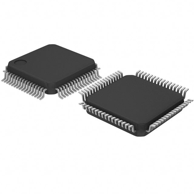
RL78/G14 1. OUTLINE <R> Table 1 - 1 List of Ordering Part Numbers (8/12) Pin Fields of Package Ordering Part Number RENESAS Code count Application Note 64 pins 64-pin plastic A R5F104LCAFA#V0, R5F104LDAFA#V0, R5F104LEAFA#V0, PLQP0064JA-A LQFP R5F104LFAFA#V0, R5F104LGAFA#V0, R5F104LHAFA#V0, (12 12 mm, R5F104LJAFA#V0 0.65 mm pitch) R5F104LCAFA#X0, R5F104LDAFA#X0, R5F104LEAFA#X0, R5F104LFAFA#X0, R5F104LGAFA#X0, R5F104LHAFA#X0, R5F104LJAFA#X0 R5F104LCAFA#30, R5F104LDAFA#30, R5F104LEAFA#30, R5F104LFAFA#30, R5F104LGAFA#30, R5F104LHAFA#30, R5F104LJAFA#30, R5F104LKAFA#30, R5F104LLAFA#30 R5F104LCAFA#50, R5F104LDAFA#50, R5F104LEAFA#50, R5F104LFAFA#50, R5F104LGAFA#50, R5F104LHAFA#50, R5F104LJAFA#50, R5F104LKAFA#50, R5F104LLAFA#50 D R5F104LCDFA#V0, R5F104LDDFA#V0, R5F104LEDFA#V0, R5F104LFDFA#V0, R5F104LGDFA#V0, R5F104LHDFA#V0, R5F104LJDFA#V0 R5F104LCDFA#X0, R5F104LDDFA#X0, R5F104LEDFA#X0, R5F104LFDFA#X0, R5F104LGDFA#X0, R5F104LHDFA#X0, R5F104LJDFA#X0 R5F104LCDFA#30, R5F104LDDFA#30, R5F104LEDFA#30, R5F104LFDFA#30, R5F104LGDFA#30, R5F104LHDFA#30, R5F104LJDFA#30 R5F104LCDFA#50, R5F104LDDFA#50, R5F104LEDFA#50, R5F104LFDFA#50, R5F104LGDFA#50, R5F104LHDFA#50, R5F104LJDFA#50 G R5F104LCGFA#V0, R5F104LDGFA#V0, R5F104LEGFA#V0, R5F104LFGFA#V0, R5F104LGGFA#V0, R5F104LHGFA#V0, R5F104LJGFA#V0 R5F104LCGFA#X0, R5F104LDGFA#X0, R5F104LEGFA#X0, R5F104LFGFA#X0, R5F104LGGFA#X0, R5F104LHGFA#X0, R5F104LJGFA#X0 R5F104LCGFA#30, R5F104LDGFA#30, R5F104LEGFA#30, R5F104LFGFA#30, R5F104LGGFA#30, R5F104LHGFA#30, R5F104LJGFA#30, R5F104LKGFA#30, R5F104LLGFA#30 R5F104LCGFA#50, R5F104LDGFA#50, R5F104LEGFA#50, R5F104LFGFA#50, R5F104LGGFA#50, R5F104LHGFA#50, R5F104LJGFA#50, R5F104LKGFA#50, R5F104LLGFA#50 Note For the fields of application, refer to Figure 1 - 1 Part Number, Memory Size, and Package of RL78/G14. Caution The ordering part numbers represent the numbers at the time of publication. For the latest ordering part numbers, refer to the target product page of the Renesas Electronics website. R01DS0053EJ0331 Rev. 3.31 Page 11 of 217 Feb 14, 2020
RL78/G14 1. OUTLINE <R> Table 1 - 1 List of Ordering Part Numbers (9/12) Pin Fields of Package Ordering Part Number RENESAS Code count Application Note 64 pins 64-pin plastic A R5F104LCAFB#V0, R5F104LDAFB#V0, R5F104LEAFB#V0, PLQP0064KF-A LFQFP R5F104LFAFB#V0, R5F104LGAFB#V0, R5F104LHAFB#V0, (10 10 mm, R5F104LJAFB#V0 0.5 mm pitch) R5F104LCAFB#X0, R5F104LDAFB#X0, R5F104LEAFB#X0, R5F104LFAFB#X0, R5F104LGAFB#X0, R5F104LHAFB#X0, R5F104LJAFB#X0 R5F104LCAFB#30, R5F104LDAFB#30, R5F104LEAFB#30, PLQP0064KB-C R5F104LFAFB#30, R5F104LGAFB#30, R5F104LHAFB#30, R5F104LJAFB#30, R5F104LKAFB#30, R5F104LLAFB#30 R5F104LCAFB#50, R5F104LDAFB#50, R5F104LEAFB#50, R5F104LFAFB#50, R5F104LGAFB#50, R5F104LHAFB#50, R5F104LJAFB#50, R5F104LKAFB#50, R5F104LLAFB#50 D R5F104LCDFB#V0, R5F104LDDFB#V0, R5F104LEDFB#V0, PLQP0064KF-A R5F104LFDFB#V0, R5F104LGDFB#V0, R5F104LHDFB#V0, R5F104LJDFB#V0 R5F104LCDFB#X0, R5F104LDDFB#X0, R5F104LEDFB#X0, R5F104LFDFB#X0, R5F104LGDFB#X0, R5F104LHDFB#X0, R5F104LJDFB#X0 R5F104LCDFB#30, R5F104LDDFB#30, R5F104LEDFB#30, PLQP0064KB-C R5F104LFDFB#30, R5F104LGDFB#30, R5F104LHDFB#30, R5F104LJDFB#30 R5F104LCDFB#50, R5F104LDDFB#50, R5F104LEDFB#50, R5F104LFDFB#50, R5F104LGDFB#50, R5F104LHDFB#50, R5F104LJDFB#50 G R5F104LCGFB#V0, R5F104LDGFB#V0, R5F104LEGFB#V0, PLQP0064KF-A R5F104LFGFB#V0, R5F104LGGFB#V0, R5F104LHGFB#V0, R5F104LJGFB#V0 R5F104LCGFB#X0, R5F104LDGFB#X0, R5F104LEGFB#X0, R5F104LFGFB#X0, R5F104LGGFB#X0, R5F104LHGFB#X0, R5F104LJGFB#X0 R5F104LCGFB#30, R5F104LDGFB#30, R5F104LEGFB#30, PLQP0064KB-C R5F104LFGFB#30, R5F104LGGFB#30, R5F104LHGFB#30, R5F104LJGFB#30, R5F104LKGFB#30, R5F104LLGFB#30 R5F104LCGFB#50, R5F104LDGFB#50, R5F104LEGFB#50, R5F104LFGFB#50, R5F104LGGFB#50, R5F104LHGFB#50, R5F104LJGFB#50, R5F104LKGFB#50, R5F104LLGFB#50 Note For the fields of application, refer to Figure 1 - 1 Part Number, Memory Size, and Package of RL78/G14. Caution The ordering part numbers represent the numbers at the time of publication. For the latest ordering part numbers, refer to the target product page of the Renesas Electronics website. R01DS0053EJ0331 Rev. 3.31 Page 12 of 217 Feb 14, 2020
RL78/G14 1. OUTLINE <R> Table 1 - 1 List of Ordering Part Numbers (10/12) Pin Fields of Package Ordering Part Number RENESAS Code count Application Note 64 pins 64-pin plastic A R5F104LCALA#U0, R5F104LDALA#U0, R5F104LEALA#U0, PWLG0064KA-A FLGA R5F104LFALA#U0, R5F104LGALA#U0, R5F104LHALA#U0, (5 5 mm, R5F104LJALA#U0, R5F104LKALA#U0, R5F104LLALA#U0 0.5 mm pitch) R5F104LCALA#W0, R5F104LDALA#W0, R5F104LEALA#W0, R5F104LFALA#W0, R5F104LGALA#W0, R5F104LHALA#W0, R5F104LJALA#W0, R5F104LKALA#W0, R5F104LLALA#W0 G R5F104LCGLA#U0, R5F104LDGLA#U0, R5F104LEGLA#U0, R5F104LFGLA#U0, R5F104LGGLA#U0, R5F104LHGLA#U0, R5F104LJGLA#U0, R5F104LKGLA#U0, R5F104LLGLA#U0 R5F104LCGLA#W0, R5F104LDGLA#W0, R5F104LEGLA#W0, R5F104LFGLA#W0, R5F104LGGLA#W0, R5F104LHGLA#W0, R5F104LJGLA#W0, R5F104LKGLA#W0, R5F104LLGLA#W0 64-pin plastic A R5F104LCAFP#V0, R5F104LDAFP#V0, R5F104LEAFP#V0, PLQP0064GA-A LQFP R5F104LFAFP#V0, R5F104LGAFP#V0, R5F104LHAFP#V0, (14 14 mm, R5F104LJAFP#V0 0.8 mm pitch) R5F104LCAFP#X0, R5F104LDAFP#X0, R5F104LEAFP#X0, R5F104LFAFP#X0, R5F104LGAFP#X0, R5F104LHAFP#X0, R5F104LJAFP#X0 R5F104LCAFP#30, R5F104LDAFP#30, R5F104LEAFP#30, R5F104LFAFP#30, R5F104LGAFP#30, R5F104LHAFP#30, R5F104LJAFP#30 R5F104LCAFP#50, R5F104LDAFP#50, R5F104LEAFP#50, R5F104LFAFP#50, R5F104LGAFP#50, R5F104LHAFP#50, R5F104LJAFP#50 D R5F104LCDFP#V0, R5F104LDDFP#V0, R5F104LEDFP#V0, R5F104LFDFP#V0, R5F104LGDFP#V0, R5F104LHDFP#V0, R5F104LJDFP#V0 R5F104LCDFP#X0, R5F104LDDFP#X0, R5F104LEDFP#X0, R5F104LFDFP#X0, R5F104LGDFP#X0, R5F104LHDFP#X0, R5F104LJDFP#X0 R5F104LCDFP#30, R5F104LDDFP#30, R5F104LEDFP#30, R5F104LFDFP#30, R5F104LGDFP#30, R5F104LHDFP#30, R5F104LJDFP#30 R5F104LCDFP#50, R5F104LDDFP#50, R5F104LEDFP#50, R5F104LFDFP#50, R5F104LGDFP#50, R5F104LHDFP#50, R5F104LJDFP#50 G R5F104LCGFP#V0, R5F104LDGFP#V0, R5F104LEGFP#V0, R5F104LFGFP#V0, R5F104LGGFP#V0, R5F104LHGFP#V0, R5F104LJGFP#V0 R5F104LCGFP#X0, R5F104LDGFP#X0, R5F104LEGFP#X0, R5F104LFGFP#X0, R5F104LGGFP#X0, R5F104LHGFP#X0, R5F104LJGFP#X0 R5F104LCGFP#30, R5F104LDGFP#30, R5F104LEGFP#30, R5F104LFGFP#30, R5F104LGGFP#30, R5F104LHGFP#30, R5F104LJGFP#30 R5F104LCGFP#50, R5F104LDGFP#50, R5F104LEGFP#50, R5F104LFGFP#50, R5F104LGGFP#50, R5F104LHGFP#50, R5F104LJGFP#50 Note For the fields of application, refer to Figure 1 - 1 Part Number, Memory Size, and Package of RL78/G14. Caution The ordering part numbers represent the numbers at the time of publication. For the latest ordering part numbers, refer to the target product page of the Renesas Electronics website. R01DS0053EJ0331 Rev. 3.31 Page 13 of 217 Feb 14, 2020
RL78/G14 1. OUTLINE <R> Table 1 - 1 List of Ordering Part Numbers (11/12) Pin Fields of Package Ordering Part Number RENESAS Code count Application Note 80 pins 80-pin plastic A R5F104MFAFB#V0, R5F104MGAFB#V0, R5F104MHAFB#V0, PLQP0080KE-A LFQFP R5F104MJAFB#V0 (12 12 mm, R5F104MFAFB#X0, R5F104MGAFB#X0, R5F104MHAFB#X0, 0.5 mm pitch) R5F104MJAFB#X0 R5F104MFAFB#30, R5F104MGAFB#30, R5F104MHAFB#30, PLQP0080KB-B R5F104MJAFB#30, R5F104MKAFB#30, R5F104MLAFB#30 R5F104MFAFB#50, R5F104MGAFB#50, R5F104MHAFB#50 R5F104MJAFB#50, R5F104MKAFB#50, R5F104MLAFB#50 D R5F104MFDFB#V0, R5F104MGDFB#V0, R5F104MHDFB#V0, PLQP0080KE-A R5F104MJDFB#V0 R5F104MFDFB#X0, R5F104MGDFB#X0, R5F104MHDFB#X0, R5F104MJDFB#X0 R5F104MFDFB#30, R5F104MGDFB#30, R5F104MHDFB#30, PLQP0080KB-B R5F104MJDFB#30 R5F104MFDFB#50, R5F104MGDFB#50, R5F104MHDFB#50, R5F104MJDFB#50 G R5F104MFGFB#V0, R5F104MGGFB#V0, R5F104MHGFB#V0, PLQP0080KE-A R5F104MJGFB#V0 R5F104MFGFB#X0, R5F104MGGFB#X0, R5F104MHGFB#X0, R5F104MJGFB#X0 R5F104MFGFB#30, R5F104MGGFB#30, R5F104MHGFB#30, PLQP0080KB-B R5F104MJGFB#30, R5F104MKGFB#30, R5F104MLGFB#30 R5F104MFGFB#50, R5F104MGGFB#50, R5F104MHGFB#50, R5F104MJGFB#50, R5F104MKGFB#50, R5F104MLGFB#50 80-pin plastic A R5F104MFAFA#V0, R5F104MGAFA#V0, R5F104MHAFA#V0, PLQP0080JB-E LQFP R5F104MJAFA#V0 (14 14 mm, R5F104MFAFA#X0, R5F104MGAFA#X0, R5F104MHAFA#X0, 0.65 mm pitch) R5F104MJAFA#X0 R5F104MFAFA#30, R5F104MGAFA#30, R5F104MHAFA#30, R5F104MJAFA#30, R5F104MKAFA#30, R5F104MLAFA#30 R5F104MFAFA#50, R5F104MGAFA#50, R5F104MHAFA#50, R5F104MJAFA#50, R5F104MKAFA#50, R5F104MLAFA#50 D R5F104MFDFA#V0, R5F104MGDFA#V0, R5F104MHDFA#V0, R5F104MJDFA#V0 R5F104MFDFA#X0, R5F104MGDFA#X0, R5F104MHDFA#X0, R5F104MJDFA#X0 R5F104MFDFA#30, R5F104MGDFA#30, R5F104MHDFA#30, R5F104MJDFA#30 R5F104MFDFA#50, R5F104MGDFA#50, R5F104MHDFA#50, R5F104MJDFA#50 G R5F104MFGFA#V0, R5F104MGGFA#V0, R5F104MHGFA#V0, R5F104MJGFA#V0 R5F104MFGFA#X0, R5F104MGGFA#X0, R5F104MHGFA#X0, R5F104MJGFA#X0 R5F104MFGFA#30, R5F104MGGFA#30, R5F104MHGFA#30, R5F104MJGFA#30, R5F104MKGFA#30, R5F104MLGFA#30 R5F104MFGFA#50, R5F104MGGFA#50, R5F104MHGFA#50, R5F104MJGFA#50, R5F104MKGFA#50, R5F104MLGFA#50 Note For the fields of application, refer to Figure 1 - 1 Part Number, Memory Size, and Package of RL78/G14. Caution The ordering part numbers represent the numbers at the time of publication. For the latest ordering part numbers, refer to the target product page of the Renesas Electronics website. R01DS0053EJ0331 Rev. 3.31 Page 14 of 217 Feb 14, 2020
RL78/G14 1. OUTLINE <R> Table 1 - 1 List of Ordering Part Numbers (12/12) Pin Fields of Package Ordering Part Number RENESAS Code count Application Note 100 100-pin plastic A R5F104PFAFB#V0, R5F104PGAFB#V0, R5F104PHAFB#V0, PLQP0100KE-A pins LFQFP R5F104PJAFB#V0 (14 14 mm, R5F104PFAFB#X0, R5F104PGAFB#X0, R5F104PHAFB#X0, 0.5 mm pitch) R5F104PJAFB#X0 R5F104PFAFB#30, R5F104PGAFB#30, R5F104PHAFB#30, PLQP0100KB-B R5F104PJAFB#30, R5F104PKAFB#30, R5F104PLAFB#30 R5F104PFAFB#50, R5F104PGAFB#50, R5F104PHAFB#50, R5F104PJAFB#50, R5F104PKAFB#50, R5F104PLAFB#50 D R5F104PFDFB#V0, R5F104PGDFB#V0, R5F104PHDFB#V0, PLQP0100KE-A R5F104PJDFB#V0 R5F104PFDFB#X0, R5F104PGDFB#X0, R5F104PHDFB#X0, R5F104PJDFB#X0 R5F104PFDFB#30, R5F104PGDFB#30, R5F104PHDFB#30, PLQP0100KB-B R5F104PJDFB#30 R5F104PFDFB#50, R5F104PGDFB#50, R5F104PHDFB#50, R5F104PJDFB#50 G R5F104PFGFB#V0, R5F104PGGFB#V0, R5F104PHGFB#V0, PLQP0100KE-A R5F104PJGFB#V0 R5F104PFGFB#X0, R5F104PGGFB#X0, R5F104PHGFB#X0, R5F104PJGFB#X0 R5F104PFGFB#30, R5F104PGGFB#30, R5F104PHGFB#30, PLQP0100KB-B R5F104PJGFB#30, R5F104PKGFB#30, R5F104PLGFB#30 R5F104PFGFB#50, R5F104PGGFB#50, R5F104PHGFB#50, R5F104PJGFB#50, R5F104PKGFB#50, R5F104PLGFB#50 100-pin plastic A R5F104PFAFA#V0, R5F104PGAFA#V0, R5F104PHAFA#V0, PLQP0100JC-A LQFP R5F104PJAFA#V0 (14 20 mm, R5F104PFAFA#X0, R5F104PGAFA#X0, R5F104PHAFA#X0, 0.65 mm pitch) R5F104PJAFA#X0 R5F104PFAFA#30, R5F104PGAFA#30, R5F104PHAFA#30, R5F104PJAFA#30, R5F104PKAFA#30, R5F104PLAFA#30 R5F104PFAFA#50, R5F104PGAFA#50, R5F104PHAFA#50, R5F104PJAFA#50, R5F104PKAFA#50, R5F104PLAFA#50 D R5F104PFDFA#V0, R5F104PGDFA#V0, R5F104PHDFA#V0, R5F104PJDFA#V0 R5F104PFDFA#X0, R5F104PGDFA#X0, R5F104PHDFA#X0, R5F104PJDFA#X0 R5F104PFDFA#30, R5F104PGDFA#30, R5F104PHDFA#30, R5F104PJDFA#30 R5F104PFDFA#50, R5F104PGDFA#50, R5F104PHDFA#50, R5F104PJDFA#50 G R5F104PFGFA#V0, R5F104PGGFA#V0, R5F104PHGFA#V0, R5F104PJGFA#V0 R5F104PFGFA#X0, R5F104PGGFA#X0, R5F104PHGFA#X0, R5F104PJGFA#X0 R5F104PFGFA#30, R5F104PGGFA#30, R5F104PHGFA#30, R5F104PJGFA#30, R5F104PKGFA#30, R5F104PLGFA#30 R5F104PFGFA#50, R5F104PGGFA#50, R5F104PHGFA#50, R5F104PJGFA#50, R5F104PKGFA#50, R5F104PLGFA#50 Note For the fields of application, refer to Figure 1 - 1 Part Number, Memory Size, and Package of RL78/G14. Caution The ordering part numbers represent the numbers at the time of publication. For the latest ordering part numbers, refer to the target product page of the Renesas Electronics website. R01DS0053EJ0331 Rev. 3.31 Page 15 of 217 Feb 14, 2020
RL78/G14 1. OUTLINE 1.3 Pin Configuration (Top View) 1.3.1 30-pin products •30-pin plastic LSSOP (7.62 mm (300), 0.65 mm pitch) P20/ANI0/AVREFP 1 30 P21/ANI1/AVREFM P01/ANI16/TO00/RxD1/TRGCLKB/TRJIO0 2 29 P22/ANI2/ANO0 Note P00/ANI17/TI00/TxD1/TRGCLKA/(TRJO0) 3 28 P23/ANI3 P120/ANI19/VCOUT0 Note 4 27 P147/ANI18/VCOUT1 Note P40/TOOL0 5 26 P10/SCK11/SCL11/TRDIOD1 P137R/IENSTEPT0 67 (TopRL7 2254 PP1112//SSIO1111/S/TDRAD1I1O/TBR1D/IVIORCE1F1 Note P122/X2P/E1R2XE1C/GXLCK1 8910 View)8/G14 222321 PPP111534///PTRxCxDDL22B//USSOZI2120/0S/S/CTDRKA2D20I0O/S/TACR1L/DI2VI0OC/TDMR0PD/(1SI ONCoBtLe0A/(0S)DAA0) VSS 11 20 P16/TI01/TO01/INTP5/TRDIOC0/IVREF0 Note/(RXD0) VDD 12 19 P17/TI02/TO02/TRDIOA0/TRDCLK/IVCMP0 Note/(TXD0) P60/SCLA0 13 18 P51/INTP2/SO00/TxD0/TOOLTxD/TRGIOB P61/SDAA0 14 17 P50/INTP1/SI00/RxD0/TOOLRxD/SDA00/TRGIOA/(TRJO0) P31/TI03/TO03/INTP4/PCLBUZ0/SSI00/(TRJIO0) 15 16 P30/INTP3/SCK00/SCL00/TRJO0 Note Mounted on the 96 KB or more code flash memory products. Caution Connect the REGC pin to VSS pin via a capacitor (0.47 to 1 F). Remark 1. For pin identification, see 1.4 Pin Identification. Remark 2. Functions in parentheses in the above figure can be assigned via settings in the peripheral I/O redirection register 0, 1 (PIOR0, 1). R01DS0053EJ0331 Rev. 3.31 Page 16 of 217 Feb 14, 2020
RL78/G14 1. OUTLINE 1.3.2 32-pin products •32-pin plastic HWQFN (5 5 mm, 0.5 mm pitch) 0) 0)XD SCK11/SCL11/TRDIOD1SI11/SDA11/TRDIOC1NoteSO11/TRDIOB1/IVREF1NoteTxD2/SO20/TRDIOA1/IVCMP1 RxD2/SI20/SDA20/TRDIOD0/(SCLA0)PCLBUZ1/SCK20/SCL20/TRDIOB0/(SDAA0)Note/(RXDTI01/TO01/INTP5/TRDIOC0/IVREF0NoteTI02/TO02/TRDIOA0/TRDCLK/IVCMP0/(T 0/1/2/3/ 4/5/6/7/ 1111 1111 PPPP PPPP exposed die pad 2423222120191817 P147/ANI18/VCOUT1Note 25 16 P51/INTP2/SO00/TxD0/TOOLTxD/TRGIOB P23/ANI3/ANO1Note 26 15 P50/INTP1/SI00/RxD0/TOOLRxD/SDA00/TRGIOA/(TRJO0) P22/ANI2/ANO0Note 27 14 P30/INTP3/SCK00/SCL00/TRJO0 P21/ANI1/AVREFM 28 RL78/G14 13 P70 P20/ANI0/AVREFP 29 (Top View) 12 P31/TI03/TO03/INTP4/PCLBUZ0/(TRJIO0) P01/ANI16/TO00/RxD1/TRGCLKB/TRJIO0 30 11 P62/SSI00 P00/ANI17/TI00/TxD1/TRGCLKA/(TRJO0) 31 10 P61/SDAA0 P120/ANI19/VCOUT0Note 32 9 P60/SCLA0 1 2 3 4 5 6 7 8 0T0K1C S D 0/TOOLRESE37/INTP2/EXCLP121/XREG VSVD 4 1X P P2/ 2 1 P Note Mounted on the 96 KB or more code flash memory products. Caution Connect the REGC pin to VSS pin via a capacitor (0.47 to 1 F). Remark 1. For pin identification, see 1.4 Pin Identification. Remark 2. Functions in parentheses in the above figure can be assigned via settings in the peripheral I/O redirection register 0, 1 (PIOR0, 1). Remark 3. It is recommended to connect an exposed die pad to VSS. R01DS0053EJ0331 Rev. 3.31 Page 17 of 217 Feb 14, 2020
RL78/G14 1. OUTLINE •32-pin plastic LQFP (7 7 mm, 0.8 mm pitch) 0) 0)xD SCK11/SCL11/TRDIOD1SI11/SDA11/TRDIOC1NoteSO11/TRDIOB1/IVREF1 NoteTxD2/SO20/TRDIOA1/IVCMP1 RxD2/SI20/SDA20/TRDIOD0/(SCLA0)PCLBUZ1/SCK20/SCL20/TRDIOB0/(SDAA0)Note/(RxDTI01/TO01/INTP5/TRDIOC0/IVREF0 NoteTI02/TO02/TRDIOA0/TRDCLK/IVCMP0 /(T 0/1/2/3/ 4/5/6/7/ 1111 1111 PPPP PPPP 2423222120191817 P147/ANI18/VCOUT1 Note 25 16 P51/INTP2/SO00/TxD0/TOOLTxD/TRGIOB P23/ANI3/ANO1 Note 26 15 P50/INTP1/SI00/RxD0/TOOLRxD/SDA00/TRGIOA/(TRJO0) P22/ANI2/ANO0 Note 27 14 P30/INTP3/SCK00/SCL00/TRJO0 P21/ANI1/AVREFM 28 (RTLo7p8 V/Gie1w4) 13 P70 P20/ANI0/AVREFP 29 12 P31/TI03/TO03/INTP4/PCLBUZ0/(TRJIO0) P01/ANI16/TO00/RxD1/TRGCLKB/TRJIO0 30 11 P62/SSI00 P00/ANI17/TI00/TxD1/TRGCLKA/(TRJO0) 31 10 P61/SDAA0 P120/ANI19/VCOUT0 Note 32 9 P60/SCLA0 1 2 3 4 5 6 7 8 0T0K1C S D 0/TOOLRESE37/INTP2/EXCLP121/XREG VSVD 4 1X P P2/ 2 1 P Note Mounted on the 96 KB or more code flash memory products. Caution Connect the REGC pin to VSS pin via a capacitor (0.47 to 1 F). Remark 1. For pin identification, see 1.4 Pin Identification. Remark 2. Functions in parentheses in the above figure can be assigned via settings in the peripheral I/O redirection register 0, 1 (PIOR0, 1). R01DS0053EJ0331 Rev. 3.31 Page 18 of 217 Feb 14, 2020
RL78/G14 1. OUTLINE 1.3.3 36-pin products •36-pin plastic WFLGA (4 × 4 mm, 0.5 mm pitch) Top View Bottom View 6 5 RL78/G14 4 (Top View) 3 2 1 A B C D E F F E D C B A INDEX MARK A B C D E F P60/SCLA0 VDD P121/X1 P122/X2/EXCLK P137/INTP0 P40/TOOL0 6 6 P62/SSI00 P61/SDAA0 VSS REGC RESET P120/ANI19/ 5 VCOUT0 Note 5 P72/SO21 P71/SI21/ P14/RxD2/SI20/ P31/TI03/TO03/ P00/TI00/TxD1/ P01/TO00/ 4 SDA21 SDA20/TRDIOD0/ INTP4/PCLBUZ0/ TRGCLKA/ RxD1/TRGCLKB/ 4 (SCLA0) (TRJIO0) (TRJO0) TRJIO0 P50/INTP1/ P70/SCK21/ P15/PCLBUZ1/ P22/ANI2/ P20/ANI0/ P21/ANI1/ SI00/RxD0/ SCL21 SCK20/SCL20/ ANO0 Note AVREFP AVREFM 3 TOOLRxD/ TRDIOB0/ 3 SDA00/TRGIOA/ (SDAA0) (TRJO0) P30/INTP3/ P16/TI01/TO01/ P12/SO11/ P11/SI11/ P24/ANI4 P23/ANI3/ SCK00/SCL00/ INTP5/TRDIOC0/ TRDIOB1/ SDA11/ ANO1 Note 2 2 TRJO0 IVREF0 Note/ IVREF1 Note TRDIOC1 (RXD0) P51/INTP2/ P17/TI02/TO02/ P13/TxD2/ P10/SCK11/ P147/ANI18/ P25/ANI5 SO00/TxD0/ TRDIOA0/ SO20/TRDIOA1/ SCL11/ VCOUT1 Note 1 TOOLTxD/ TRDCLK/ IVCMP1 Note TRDIOD1 1 TRGIOB IVCMP0 Note/ (TXD0) A B C D E F Note Mounted on the 96 KB or more code flash memory products. Caution Connect the REGC pin to VSS pin via a capacitor (0.47 to 1 F). Remark 1. For pin identification, see 1.4 Pin Identification. Remark 2. Functions in parentheses in the above figure can be assigned via settings in the peripheral I/O redirection register 0, 1 (PIOR0, 1). R01DS0053EJ0331 Rev. 3.31 Page 19 of 217 Feb 14, 2020
RL78/G14 1. OUTLINE 1.3.4 40-pin products •40-pin plastic HWQFN (6 6 mm, 0.5 mm pitch) 0) 0)XD Note47/ANI18/VCOUT10/SCK11/SCL11/TRDIOD11/SI11/SDA11/TRDIOC1Note2/SO11/TRDIOB1/IVREF1Note3/TxD2/SO20/TRDIOA1/IVCMP14/RxD2/SI20/SDA20/TRDIOD0/(SCLA0)5/PCLBUZ1/SCK20/SCL20/TRDIOB0/(SDAA0)Note6/TI01/TO01/INTP5/TRDIOC0/IVREF0/(RXDNote7/TI02/TO02/TRDIOA0/TRDCLK/IVCMP0/(T1/INTP2/SO00/TxD0/TOOLTxD/TRGIOB 1111111115 PPPPPPPPPP 30292827262524232221 P26/ANI6 31 20 P50/INTP1/SI00/RxD0/TOOLRxD/SDA00/TRGIOA/(TRJO0) P25/ANI5 32 exposed die pad 19 P30/INTP3/RTC1HZ/SCK00/SCL00/TRJO0 P24/ANI4 33 18 P70/KR0/SCK21/SCL21 P23/ANI3/ANO1Note 34 17 P71/KR1/SI21/SDA21 P22/ANI2/ANO0Note 35 RL78/G14 16 P72/KR2/SO21 P21/ANI1/AVREFM 36 (Top View) 15 P73/KR3 P20/ANI0/AVREFP 37 14 P31/TI03/TO03/INTP4/PCLBUZ0/(TRJIO0) P01/TO00/RxD1/TRGCLKB/TRJIO0 38 13 P62/SSI00 P00/TI00/TxD1/TRGCLKA/(TRJO0) 39 12 P61/SDAA0 P120/ANI19/VCOUT0Note 40 11 P60/SCLA0 1 2 3 4 5 6 7 8 910 0TS10K1C S D 40/TOOLRESE2/EXCLKP123/XT137/INTPX2/EXCLP121/XREGVSVD P XT P22/ 24/ P1 1 P Note Mounted on the 96 KB or more code flash memory products. Caution Connect the REGC pin to VSS pin via a capacitor (0.47 to 1 F). Remark 1. For pin identification, see 1.4 Pin Identification. Remark 2. Functions in parentheses in the above figure can be assigned via settings in the peripheral I/O redirection register 0, 1 (PIOR0, 1). Remark 3. It is recommended to connect an exposed die pad to VSS. R01DS0053EJ0331 Rev. 3.31 Page 20 of 217 Feb 14, 2020
RL78/G14 1. OUTLINE 1.3.5 44-pin products •44-pin plastic LQFP (10 × 10 mm, 0.8 mm pitch) 0) 0)XD Note47/ANI18/VCOUT1460/SCK11/SCL11/TRDIOD11/SI11/SDA11/TRDIOC1Note2/SO11/TRDIOB1/IVREF1Note3/TxD2/SO20/TRDIOA1/IVCMP14/RxD2/SI20/SDA20/TRDIOD0/(SCLA0)5/PCLBUZ1/SCK20/SCL20/TRDIOB0/(SDAA0) Note6/TI01/TO01/INTP5/TRDIOC0/IVREF0/(RXD Note7/TI02/TO02/TRDIOA0/TRDCLK/IVCMP0/(T1/INTP2/SO00/TxD0/TOOLTxD/TRGIOB 11111111115 PPPPPPPPPPP 3332313029282726252423 P27/ANI7 34 22 P50/INTP1/SI00/RxD0/TOOLRxD/SDA00/TRGIOA/(TRJO0) P26/ANI6 35 21 P30/INTP3/RTC1HZ/SCK00/SCL00/TRJO0 P25/ANI5 36 20 P70/KR0/SCK21/SCL21 P24/ANI4 37 19 P71/KR1/SI21/SDA21 P23/ANI3/ANO1Note 38 RL78/G14 18 P72/KR2/SO21 P22/ANI2/ANO0Note 39 (Top View) 17 P73/KR3 P21/ANI1/AVREFM 40 16 P31/TI03/TO03/INTP4/PCLBUZ0/(TRJIO0) P20/ANI0/AVREFP 41 15 P63 P01/TO00/RxD1/TRGCLKB/TRJIO0 42 14 P62/SSI00 P00/TI00/TxD1/TRGCLKA/(TRJO0) 43 13 P61/SDAA0 P120/ANI19/VCOUT0Note 44 12 1 2 3 4 5 6 7 8 9 1011 P60/SCLA0 P41/(TRJIO0)P40/TOOL0RESETXT2/EXCLKSP123/XT1P137/INTP022/X2/EXCLKP121/X1REGCVSSVDD 24/ P1 1 P Note Mounted on the 96 KB or more code flash memory products. Caution Connect the REGC pin to VSS pin via a capacitor (0.47 to 1 F). Remark 1. For pin identification, see 1.4 Pin Identification. Remark 2. Functions in parentheses in the above figure can be assigned via settings in the peripheral I/O redirection register 0, 1 (PIOR0, 1). R01DS0053EJ0331 Rev. 3.31 Page 21 of 217 Feb 14, 2020
RL78/G14 1. OUTLINE 1.3.6 48-pin products •48-pin plastic LFQFP (7 7 mm, 0.5 mm pitch) 0)O0 A/(TRJOKB/TRJI KL 40/PCLBUZ0/INTP6 0/TI00/TxD1/TRGCL1/TO00/RxD1/TRGC30 0/ANI0/AVREFP1/ANI1/AVREFMNote 12/ANI2/ANO0 Note 13/ANI3/ANO1 4/ANI45/ANI5 6/ANI67/ANI7 1 001 22 22 22 22 P PPP PP PP PP PP 36 3534333231302928272625 P120/ANI19/VCOUT0 Note 1 37 24 P147/ANI18/VCOUT1Note 1 P41/(TRJIO0) 38 23 P146 P40/TOOL0 39 22 P10/SCK11/SCL11/TRDIOD1 RESET 40 21 P11/SI11/SDA11/TRDIOC1/(RxD0_1)Note 2 P124/XT2/EXCLKS 41 20 P12/SO11/TRDIOB1/IVREF1Note 1 /(TxD0_1)Note 2 P123/XT1 42 RL78/G14 19 P13/TxD2/SO20/TRDIOA1/IVCMP1Note 1 P137/INTP0 43 (Top View) 18 P14/RxD2/SI20/SDA20/TRDIOD0/(SCLA0) P122/X2/EXCLK 44 17 P15/PCLBUZ1/SCK20/SCL20/TRDIOB0/(SDAA0) P121/X1 45 16 P16/TI01/TO01/INTP5/TRDIOC0/IVREF0Note 1/(RXD0) REGC 46 15 P17/TI02/TO02/TRDIOA0/TRDCLK/IVCMP0 Note 1/(TXD0) VSS 47 14 P51/INTP2/SO00/TxD0/TOOLTxD/TRGIOB VDD 48 13 P50/INTP1/SI00/RxD0/TOOLRxD/SDA00/TRGIOA/(TRJO0) 1 2 3 4 5 6 7 8 9 101112 P60/SCLA0 P61/SDAA0P62/SSI00P6303/INTP4/(PCLBUZ0)/(TRJIO0) P75/KR5/INTP9/SCK01/SCL01P74/KR4/INTP8/SI01/SDA01P73/KR3/SO01P72/KR2/SO21P71/KR1/SI21/SDA21P70/KR0/SCK21/SCL21RTC1HZ/SCK00/SCL00/TRJO0 3/TO TP3/ 0 N P31/TI P30/I Note 1. Mounted on the 96 KB or more code flash memory products. Note 2. Mounted on the 384 KB or more code flash memory products. Caution Connect the REGC pin to VSS pin via a capacitor (0.47 to 1 F). Remark 1. For pin identification, see 1.4 Pin Identification. Remark 2. Functions in parentheses in the above figure can be assigned via settings in the peripheral I/O redirection register 0, 1 (PIOR0, 1). R01DS0053EJ0331 Rev. 3.31 Page 22 of 217 Feb 14, 2020
RL78/G14 1. OUTLINE •48-pin plastic HWQFN (7 7 mm, 0.5 mm pitch) 0)O0 A/(TRJOKB/TRJI KL 40/PCLBUZ0/INTP6 0/TI00/TxD1/TRGCL1/TO00/RxD1/TRGC30 0/ANI0/AVREFP1/ANI1/AVREFMNote 12/ANI2/ANO0Note 13/ANI3/ANO1 4/ANI45/ANI5 6/ANI67/ANI7 1 001 22 22 22 22 P PPP PP PP PP PP 36 3534333231302928272625 P120/ANI19/VCOUT0Note 1 37 24 P147/ANI18/VCOUT1Note 1 P41/(TRJIO0) 38 exposed die pad 23 P146 P40/TOOL0 39 22 P10/SCK11/SCL11/TRDIOD1 RESET 40 21 P11/SI11/SDA11/TRDIOC1/(RxD0_1)Note 2 P124/XT2/EXCLKS 41 20 P12/SO11/TRDIOB1/IVREF1Note 1/(TxD0_1)Note 2 P123/XT1 42 RL78/G14 19 P13/TxD2/SO20/TRDIOA1/IVCMP1Note 1 P137/INTP0 43 (Top View) 18 P14/RxD2/SI20/SDA20/TRDIOD0/(SCLA0) P122/X2/EXCLK 44 17 P15/PCLBUZ1/SCK20/SCL20/TRDIOB0/(SDAA0) P121/X1 45 16 P16/TI01/TO01/INTP5/TRDIOC0/IVREF0Note 1/(RXD0) REGC 46 15 P17/TI02/TO02/TRDIOA0/TRDCLK/IVCMP0Note 1/(TXD0) VSS 47 14 P51/INTP2/SO00/TxD0/TOOLTxD/TRGIOB VDD 48 13 P50/INTP1/SI00/RxD0/TOOLRxD/SDA00/TRGIOA/(TRJO0) 1 2 3 4 5 6 7 8 9 101112 P60/SCLA0 P61/SDAA0P62/SSI00P6303/INTP4/(PCLBUZ0)/(TRJIO0) P75/KR5/INTP9/SCK01/SCL01P74/KR4/INTP8/SI01/SDA01P73/KR3/SO01P72/KR2/SO21P71/KR1/SI21/SDA21P70/KR0/SCK21/SCL21RTC1HZ/SCK00/SCL00/TRJO0 3/TO TP3/ 0 N P31/TI P30/I Note 1. Mounted on the 96 KB or more code flash memory products. Note 2. Mounted on the 384 KB or more code flash memory products. Caution Connect the REGC pin to VSS pin via a capacitor (0.47 to 1 F). Remark 1. For pin identification, see 1.4 Pin Identification. Remark 2. Functions in parentheses in the above figure can be assigned via settings in the peripheral I/O redirection register 0, 1 (PIOR0, 1). Remark 3. It is recommended to connect an exposed die pad to VSS. R01DS0053EJ0331 Rev. 3.31 Page 23 of 217 Feb 14, 2020
RL78/G14 1. OUTLINE 1.3.7 52-pin products •52-pin plastic LQFP (10 10 mm, 0.65 mm pitch) 0) O 0) RJ Note47/ANI18/VCOUT1 46 0/SCK11/SCL11/TRDIOD1 1/SI11/SDA11/TRDIOC1 Note2/SO11/TRDIOB1/IVREF1 Note3/TxD2/SO20/TRDIOA1/IVCMP1 4/RxD2/SI20/SDA20/TRDIOD0/(SCLA0) 5/PCLBUZ1/SCK20/SCL20/TRDIOB0/(SDAA0) Note/(RXD0)6/TI01/TO01/INTP5/TRDIOC0/IVREF0 Note/(TXD7/TI02/TO02/TRDIOA0/TRDCLK/IVCMP0 1/INTP2/SO00/TxD0/TOOLTxD/TRGIOB 0/INTP1/SI00/RxD0/TOOLRxD/SDA00/TRGIOA/(T 0/INTP3/RTC1HZ/SCK00/SCL00/TRJO0 1 1 1 1 1 1 1 1 1 1 5 5 3 P P P P P P P P P P P P P 39 38 37 36 35 34 33 32 31 3029 28 27 P27/ANI7 40 26 P70/KR0/SCK21/SCL21 P26/ANI6 41 25 P71/KR1/SI21/SDA21 P25/ANI5 42 24 P72/KR2/SO21 P24/ANI4 43 23 P73/KR3/SO01 P23/ANI3/ANO1 Note 44 22 P74/KR4/INTP8/SI01/SDA01 P22/ANI2/ANO0 Note 45 RL78/G14 21 P75/KR5/INTP9/SCK01/SCL01 P21/ANI1/AVREFM 46 (Top View) 20 P76/KR6/INTP10/(RXD2) P20/ANI0/AVREFP 47 19 P77/KR7/INTP11/(TXD2) P130 48 18 P31/TI03/TO03/INTP4/(PCLBUZ0)/(TRJIO0) P03/ANI16/RxD1 49 17 P63 P02/ANI17/TxD1 50 16 P62/SSI00 P01/TO00/TRGCLKB/TRJIO0 51 15 P61/SDAA0 P00/TI00/TRGCLKA/(TRJO0) 52 14 P60/SCLA0 1 2 3 4 5 6 7 8 9 1011 12 13 140/PCLBUZ0/INTP6 Note0/ANI19/VCOUT0 P41/(TRJIO0) P40/TOOL0 RESETP124/XT2/EXCLKS P123/XT1 P137/INTP0 P122/X2/EXCLK P121/X1 REGC VSS VDD P 2 1 P Note Mounted on the 96 KB or more code flash memory products. Caution Connect the REGC pin to VSS pin via a capacitor (0.47 to 1 F). Remark 1. For pin identification, see 1.4 Pin Identification. Remark 2. Functions in parentheses in the above figure can be assigned via settings in the peripheral I/O redirection register 0, 1 (PIOR0, 1). R01DS0053EJ0331 Rev. 3.31 Page 24 of 217 Feb 14, 2020
RL78/G14 1. OUTLINE 1.3.8 64-pin products •64-pin plastic LQFP (14 14 mm, 0.8 mm pitch) •64-pin plastic LQFP (12 12 mm, 0.65 mm pitch) •64-pin plastic LFQFP (10 10 mm, 0.5 mm pitch) 0) D Note 147/ANI18/VCOUT1460/SCK11/SCL11/TRDIOD1Note 21/SI11/SDA11/TRDIOC1/(RxD0_1)Note 1Note 22/SO11/TRDIOB1/IVREF1/(INTP5)/(TxD0_1)Note 13/TxD2/SO20/TRDIOA1/IVCMP14/RxD2/SI20/SDA20/TRDIOD0/(SCLA0)5/SCK20/SCL20/TRDIOB0/(SDAA0)Note 16/TI01/TO01/INTP5/TRDIOC0/IVREF0/(SI00)/(RXD0)Note 17/TI02/TO02/TRDIOA0/TRDCLK/IVCMP0/(SO00)/(TX5/(PCLBUZ1)/(SCK00)/(INTP4)4/(INTP3)3/(INTP2)2/(INTP1)1/INTP2/SO00/TxD0/TOOLTxD/TRGIOB0/INTP1/SI00/RxD0/TOOLRxD/SDA00/TRGIOA/(TRJO0) 1111111111555555 PPPPPPPPPPPPPPPP 48474645444342414039383736353433 P27/ANI7 49 32 P30/INTP3/RTC1HZ/SCK00/SCL00/TRJO0 P26/ANI6 50 31 P05/(INTP10) P25/ANI5 51 30 P06/(INTP11)/(TRJIO0) P24/ANI4 52 29 P70/KR0/SCK21/SCL21 P23/ANI3/ANO1Note 1 53 28 P71/KR1/SI21/SDA21 P22/ANI2/ANO0Note 1 54 27 P72/KR2/SO21 P21/ANI1/AVREFM 55 26 P73/KR3/SO01 P20/ANI0/AVREFP 56 RL78/G14 25 P74/KR4/INTP8/SI01/SDA01 P130 57 (Top View) 24 P75/KR5/INTP9/SCK01/SCL01 P04/SCK10/SCL10 58 23 P76/KR6/INTP10/(RXD2) P03/ANI16/SI10/RxD1/SDA10 59 22 P77/KR7/INTP11/(TXD2) P02/ANI17/SO10/TxD1 60 21 P31/TI03/TO03/INTP4/(PCLBUZ0)/(TRJIO0) P01/TO00/TRGCLKB/TRJIO0 61 20 P63 P00/TI00/TRGCLKA/(TRJO0) 62 19 P62/SSI00 P141/PCLBUZ1/INTP7 63 18 P61/SDAA0 P140/PCLBUZ0/INTP6 64 17 P60/SCLA0 1 2 3 4 5 6 7 8 910111213141516 Note 119/VCOUT0P43/(INTP9)P42/(INTP8)P41/(TRJIO0)P40/TOOL0RESET24/XT2/EXCLKSP123/XT1P137/INTP0P122/X2/EXCLKP121/X1REGCVSSEVSS0VDDEVDD0 NI P1 A 0/ 2 1 P Note 1. Mounted on the 96 KB or more code flash memory products. Note 2. Mounted on the 384 KB or more code flash memory products. Caution 1. Make EVSS0 pin the same potential as VSS pin. Caution 2. Make VDD pin the potential that is higher than EVDD0 pin. Caution 3. Connect the REGC pin to VSS pin via a capacitor (0.47 to 1 F). Remark 1. For pin identification, see 1.4 Pin Identification. Remark 2. When using the microcontroller for an application where the noise generated inside the microcontroller must be reduced, it is recommended to supply separate powers to the VDD and EVDD0 pins and connect the VSS and EVSS0 pins to separate ground lines. Remark 3. Functions in parentheses in the above figure can be assigned via settings in the peripheral I/O redirection register 0, 1 (PIOR0, 1). R01DS0053EJ0331 Rev. 3.31 Page 25 of 217 Feb 14, 2020
RL78/G14 1. OUTLINE •64-pin plastic FLGA (5 5 mm, 0.5 mm pitch) Top View Bottom View 8 7 6 RL78/G14 5 (Top View) 4 3 2 1 A B C D E F G H H G F E D C B A INDEX MARK A B C D E F G H EVDD0 EVSS0 P121/X1 P122/X2/ P137/INTP0 P123/XT1 P124/XT2/ P120/ANI19/ 8 8 EXCLK EXCLKS VCOUT0 Note 1 P60/SCLA0 VDD VSS REGC RESET P01/TO00/ P00/TI00/ P140/ 7 TRGCLKB/ TRGCLKA/ PCLBUZ0/ 7 TRJIO0 (TRJO0) INTP6 P61/SDAA0 P62/SSI00 P63 P40/TOOL0 P41/(TRJIO0) P43/(INTP9) P02/ANI17/ P141/ 6 SO10/TxD1 PCLBUZ1/ 6 INTP7 P77/KR7/ P31/TI03/ P53/(INTP2) P42/(INTP8) P03/ANI16/ P04/SCK10/ P130 P20/ANI0/ INTP11/(TXD2) TO03/INTP4/ SI10/RxD1/ SCL10 AVREFP 5 5 (PCLBUZ0)/ SDA10 (TRJIO0) P75/KR5/ P76/KR6/ P52/(INTP1) P54/(INTP3) P16/TI01/ P21/ANI1/ P22/ANI2/ P23/ANI3/ INTP9/ INTP10/ TO01/INTP5/ AVREFM ANO0 Note 1 ANO1 Note 1 4 SCK01/ (RXD2) TRDIOC0/ 4 SCL01 IVREF0 Note 1/ (SI00)/(RXD0) P70/KR0/ P73/KR3/ P74/KR4/ P17/TI02/TO02/ P15/SCK20/ P12/SO11/ P24/ANI4 P26/ANI6 SCK21/ SO01 INTP8/SI01/ TRDIOA0/ SCL20/ TRDIOB1/ 3 SCL21 SDA01 TRDCLK/ TRDIOB0/ IVREF1 Note 1/ 3 IVCMP0 Note 1/ (SDAA0) (INTP5)/ (SO00)/(TXD0) (TxD0_1) Note 2 P30/INTP3/ P72/KR2/ P71/KR1/ P06/(INTP11)/ P14/RxD2/ P11/SI11/ P25/ANI5 P27/ANI7 RTC1HZ/ SO21 SI21/SDA21 (TRJIO0) SI20/SDA20/ SDA11/ 2 2 SCK00/ TRDIOD0/ TRDIOC1/ SCL00/TRJO0 (SCLA0) (RxD0_1) Note 2 P05/(INTP10) P50/INTP1/ P51/INTP2/ P55/ P13/TxD2/ P10/SCK11/ P146 P147/ANI18/ SI00/RxD0/ SO00/TxD0/ (PCLBUZ1)/ SO20/ SCL11/ VCOUT1 Note 1 TOOLRxD/ TOOLTxD/ (SCK00)/ TRDIOA1/ TRDIOD1 1 1 SDA00/ TRGIOB (INTP4) IVCMP1 Note 1 TRGIOA/ (TRJO0) A B C D E F G H Note 1. Mounted on the 96 KB or more code flash memory products. Note 2. Mounted on the 384 KB or more code flash memory products. Caution 1. Make EVSS0 pin the same potential as VSS pin. Caution 2. Make VDD pin the potential that is higher than EVDD0 pin. Caution 3. Connect the REGC pin to VSS pin via a capacitor (0.47 to 1 F). Remark 1. For pin identification, see 1.4 Pin Identification. Remark 2. When using the microcontroller for an application where the noise generated inside the microcontroller must be reduced, it is recommended to supply separate powers to the VDD and EVDD0 pins and connect the VSS and EVSS0 pins to separate ground lines. Remark 3. Functions in parentheses in the above figure can be assigned via settings in the peripheral I/O redirection register 0, 1 (PIOR0, 1). R01DS0053EJ0331 Rev. 3.31 Page 26 of 217 Feb 14, 2020
RL78/G14 1. OUTLINE 1.3.9 80-pin products •80-pin plastic LQFP (14 14 mm, 0.65 mm pitch) •80-pin plastic LFQFP (12 12 mm, 0.5 mm pitch) D0) O0) 0)Tx RJ 53/ANI1100/ANI20/(INTP10)47/ANI18/VCOUT1461110/(INTP11)0/SCK11/SCL11/TRDIOD1Note1/SI11/SDA11/TRDIOC1/(RxD0_1)Note2/SO11/TRDIOB1/IVREF1/(INTP5)/(TxD0_1)3/TxD2/SO20/TRDIOA1/IVCMP14/RxD2/SI20/SDA20/TRDIOD0/(SCLA0)5/SCK20/SCL20/TRDIOB0/(SDAA0)6/TI01/TO01/INTP5/TRDIOC0/IVREF0/(SI00)/(RxD7/TI02/TO02/TRDIOA0/TRDCLK/IVCMP0/(SO00)/(5/(PCLBUZ1)/(SCK00)/(INTP4)4/SCK31/SCL31/(INTP3)3/SI31/SDA31/(INTP2)2/SO31/(INTP1)1/INTP2/SO00/TxD0/TOOLTxD/TRGIOB0/INTP1/SI00/RxD0/TOOLRxD/SDA00/TRGIOA/(T 11111111111111555555 PPPPPPPPPPPPPPPPPPPP 6059585756555453525150494847464544434241 P152/ANI10 61 40 P30/INTP3/RTC1HZ/SCK00/SCL00/TRJO0 P151/ANI9 62 39 P05 P150/ANI8 63 38 P06/(TRJIO0) P27/ANI7 64 37 P70/KR0/SCK21/SCL21 P26/ANI6 65 36 P71/KR1/SI21/SDA21 P25/ANI5 66 35 P72/KR2/SO21 P24/ANI4 67 34 P73/KR3 P23/ANI3/ANO1 68 33 P74/KR4/INTP8 P22/ANI2/ANO0 69 32 P75/KR5/INTP9 P21/ANI1/AVREFM 70 RL78/G14 31 P76/KR6/INTP10/(RxD2) P20/ANI0/AVREFP 71 (Top View) 30 P77/KR7/INTP11/(TxD2) P130 72 29 P67/TI13/TO13 P04/SCK10/SCL10 73 28 P66/TI12/TO12 P03/ANI16/SI10/RxD1/SDA10 74 27 P65/TI11/TO11 P02/ANI17/SO10/TxD1 75 26 P64/TI10/TO10 P01/TO00/TRGCLKB/TRJIO0 76 25 P31/TI03/TO03/INTP4/(PCLBUZ0)/(TRJIO0) P00/TI00/TRGCLKA/(TRJO0) 77 24 P63/SDAA1 P144/SO30/TxD3 78 23 P62/SSI00/SCLA1 P143/SI30/RxD3/SDA30 79 22 P61/SDAA0 P142/SCK30/SCL30 80 21 P60/SCLA0 1 2 3 4 5 6 7 8 9 1011121314151617181920 P141/PCLBUZ1/INTP7P140/PCLBUZ0/INTP6P120/ANI19/VCOUT0P45/SO01P44/SI01/SDA01SCK01/SCL01/(INTP9)P42/(INTP8)P41/(TRJIO0)P40/TOOL0RESETP124/XT2/EXCLKSP123/XT1P137/INTP0P122/X2/EXCLKP121/X1REGCVSSEVSS0VDDEVDD0 3/ 4 P Note Mounted on the 384 KB or more code flash memory products. Caution 1. Make EVSS0 pin the same potential as VSS pin. Caution 2. Make VDD pin the potential that is higher than EVDD0 pin. Caution 3. Connect the REGC pin to VSS pin via a capacitor (0.47 to 1 F). Remark 1. For pin identification, see 1.4 Pin Identification. Remark 2. When using the microcontroller for an application where the noise generated inside the microcontroller must be reduced, it is recommended to supply separate powers to the VDD and EVDD0 pins and connect the VSS and EVSS0 pins to separate ground lines. Remark 3. Functions in parentheses in the above figure can be assigned via settings in the peripheral I/O redirection register 0, 1 (PIOR0, 1). R01DS0053EJ0331 Rev. 3.31 Page 27 of 217 Feb 14, 2020
RL78/G14 1. OUTLINE 1.3.10 100-pin products •100-pin plastic LFQFP (14 14 mm, 0.5 mm pitch) 0) D 100/ANI20/(INTP10)147/ANI18/VCOUT1146/(INTP4)111110/(INTP11)10110/SCK11/SCL11/TRDIOD1Note11/SI11/SDA11/TRDIOC1/(RxD0_1)Note12/SO11/TRDIOB1/IVREF1/(INTP5)/(TxD0_1)13/TxD2/SO20/TRDIOA1/IVCMP114/RxD2/SI20/SDA20/TRDIOD0/(SCLA0)15/SCK20/SCL20/TRDIOB0/(SDAA0)16/TI01/TO01/INTP5/TRDIOC0/IVREF0/(SI00)/(RxD0)17/TI02/TO02/TRDIOA0/TRDCLK/IVCMP0/(SO00)/(Tx57/(INTP3)56/(INTP1)55/(PCLBUZ1)/(SCK00)54/SCK31/SCL3153/SI31/SDA3152/SO3151/SO00/TxD0/TOOLTxD/TRGIOB50/SI00/RxD0/TOOLRxD/SDA00/TRGIOA/(TRJO0)VDD1 30/INTP3/RTC1HZ/SCK00/SCL00/TRJO087/(INTP9) PPPPPPPPPPPPPPPPPPPPPPEPP 75747372717069686766656463626160595857565554535251 P156/ANI14 76 50 P86/(INTP8) P155/ANI13 77 49 P85/(INTP7) P154/ANI12 78 48 P84/(INTP6) P153/ANI11 79 47 P83 P152/ANI10 80 46 P82/(SO10)/(TxD1) P151/ANI9 81 45 P81/(SI10)/(RxD1)/(SDA10) P150/ANI8 82 44 P80/(SCK10)/(SCL10) P27/ANI7 83 43 EVSS1 P26/ANI6 84 42 P05 P25/ANI5 85 41 P06/(TRJIO0) P24/ANI4 86 40 P70/KR0/SCK21/SCL21 P23/ANI3/ANO1 87 RL78/G14 39 P71/KR1/SI21/SDA21 P22/ANI2/ANO0 88 (Top View) 38 P72/KR2/SO21 P21/ANI1/AVREFM 89 37 P73/KR3 P20/ANI0/AVREFP 90 36 P74/KR4/INTP8 P130 91 35 P75/KR5/INTP9 P102 92 34 P76/KR6/INTP10/(RxD2) P04/SCK10/SCL10 93 33 P77/KR7/INTP11/(TxD2) P03/ANI16/SI10/RxD1/SDA10 94 32 P67/TI13/TO13 P02/ANI17/SO10/TxD1 95 31 P66/TI12/TO12 P01/TO00/TRGCLKB/TRJIO0 96 30 P65/TI11/TO11 P00/TI00/TRGCLKA/(TRJO0) 97 29 P64/TI10/TO10 P145 98 28 P31/TI03/TO03/INTP4/(PCLBUZ0)/(TRJIO0) P144/SO30/TxD3 99 27 P63/SDAA1 P143/SI30/RxD3/SDA30 100 26 P62/SSI00/SCLA1 1 2 3 4 5 6 7 8 9 10111213141516171819202122232425 P142/SCK30/SCL30P141/PCLBUZ1/INTP7P140/PCLBUZ0/INTP6P120/ANI19/VCOUT0P47/INTP2P46/INTP1P45/SO01P44/SI01/SDA01P43/SCK01/SCL01P42P41/(TRJIO0)P40/TOOL0RESETP124/XT2/EXCLKSP123/XT1P137/INTP0P122/X2/EXCLKP121/X1REGCVSSEVSS0VDDEVDD0P60/SCLA0P61/SDAA0 Note Mounted on the 384 KB or more code flash memory products. Caution 1. Make EVSS0, EVSS1 pins the same potential as VSS pin. Caution 2. Make VDD pin the potential that is higher than EVDD0, EVDD1 pins (EVDD0 = EVDD1). Caution 3. Connect the REGC pin to VSS pin via a capacitor (0.47 to 1 F). Remark 1. For pin identification, see 1.4 Pin Identification. Remark 2. When using the microcontroller for an application where the noise generated inside the microcontroller must be reduced, it is recommended to supply separate powers to the VDD, EVDD0 and EVDD1 pins and connect the VSS, EVSS0 and EVSS1 pins to separate ground lines. Remark 3. Functions in parentheses in the above figure can be assigned via settings in the peripheral I/O redirection register 0, 1 (PIOR0, 1). R01DS0053EJ0331 Rev. 3.31 Page 28 of 217 Feb 14, 2020
RL78/G14 1. OUTLINE •100-pin plastic LQFP (14 20 mm, 0.65 mm pitch) P140/PCLBUZ0/INTP6P141/PCLBUZ1/INTP7P142/SCK30/SCL30P143/SI30/RxD3/SDA30P144/SO30/TxD3P145P00/TI00/TRGCLKA/(TRJO0)P01/TO00/TRGCLKB/TRJIO0P02/ANI17/SO10/TxD1P03/ANI16/SI10/RxD1/SDA10P04/SCK10/SCL10P102P130P20/ANI0/AVREFPP21/ANI1/AVREFMP22/ANI2/ANO0P23/ANI3/ANO1P24/ANI4P25/ANI5P26/ANI6P27/ANI7P150/ANI8P151/ANI9P152/ANI10P153/ANI11P154/ANI12P155/ANI13P156/ANI14P100/ANI20/(INTP10)P147/ANI18/VCOUT1 807978777675747372717069686766656463626160595857565554535251 P120/ANI19/VCOUT0 81 50 P146/(INTP4) P47/INTP2 82 49 P111 P46/INTP1 83 48 P110/(INTP11) P45/SO01 84 47 P101 P44/SI01/SDA01 85 46 P10/SCK11/SCL11/TRDIOD1 P43/SCK01/SCL01 86 45 P11/SI11/SDA11/TRDIOC1/(RxD0_1)Note P42 87 44 P12/SO11/TRDIOB1/IVREF1/(INTP5)/(TxD0_1)Note P41/(TRJIO0) 88 43 P13/TxD2/SO20/TRDIOA1/IVCMP1 P40/TOOL0 89 RL78/G14 42 P14/RxD2/SI20/SDA20/TRDIOD0/(SCLA0) RESET 90 41 P15/SCK20/SCL20/TRDIOB0/(SDAA0) P124/XT2/EXCLKS 91 (Top View) 40 P16/TI01/TO01/INTP5/TRDIOC0/IVREF0/(SI00)/(RxD0) P123/XT1 92 39 P17/TI02/TO02/TRDIOA0/TRDCLK/IVCMP0/(SO00)/(TxD0) P137/INTP0 93 38 P57/(INTP3) P122/X2/EXCLK 94 37 P56/(INTP1) P121/X1 95 36 P55/(PCLBUZ1)/(SCK00) REGC 96 35 P54/SCK31/SCL31 VSS 97 34 P53/SI31/SDA31 EVSS0 98 33 P52/SO31 VDD 99 32 P51/SO00/TxD0/TOOLTxD/TRGIOB EVDD0 100 31 P50/SI00/RxD0/TOOLRxD/SDA00/TRGIOA/(TRJO0) 1 2 3 4 5 6 7 8 9101112131415161718192021222324252627282930 P60/SCLA0P61/SDAA0/SCLA1P62/SSI00P63/SDAA1P31/TI03/TO03/INTP4/(PCLBUZ0)/(TRJIO0)P64/TI10/TO10P65/TI11/TO11P66/TI12/TO12P67/TI13/TO13P77/KR7/INTP11/(TxD2)P76/KR6/INTP10/(RxD2)P75/KR5/INTP9P74/KR4/INTP8P73/KR3P72/KR2/SO21P71/KR1/SI21/SDA21P70/KR0/SCK21/SCL21P06/(TRJIO0)P05EVSS1P80/(SCK10)/(SCL10)P81/(SI10)/(RxD1)/(SDA10)P82/(SO10)/(TxD1)P83P84/(INTP6)P85/(INTP7)P86/(INTP8)P87/(INTP9)P30/INTP3/RTC1HZ/SCK00/SCL00/TRJO0EVDD1 Note Mounted on the 384 KB or more code flash memory products. Caution 1. Make EVSS0, EVSS1 pins the same potential as VSS pin. Caution 2. Make VDD pin the potential that is higher than EVDD0, EVDD1 pins (EVDD0 = EVDD1). Caution 3. Connect the REGC pin to VSS pin via a capacitor (0.47 to 1 F). Remark 1. For pin identification, see 1.4 Pin Identification. Remark 2. When using the microcontroller for an application where the noise generated inside the microcontroller must be reduced, it is recommended to supply separate powers to the VDD, EVDD0 and EVDD1 pins and connect the VSS, EVSS0 and EVSS1 pins to separate ground lines. Remark 3. Functions in parentheses in the above figure can be assigned via settings in the peripheral I/O redirection register 0, 1 (PIOR0, 1). R01DS0053EJ0331 Rev. 3.31 Page 29 of 217 Feb 14, 2020
RL78/G14 1. OUTLINE 1.4 Pin Identification ANI0 to ANI14, RxD0 to RxD3: Receive data ANI16 to ANI20: Analog output SCK00, SCK01, SCK10, ANO0, ANO1: Analog output SCK11, SCK20, SCK21, AVREFM: A/D converter reference SCK30, SCK31, potential ( side) input SCLA0, SCLA1: Serial clock input/output AVREFP: A/D converter reference SCL00, SCL01, SCL10, SCL11, potential (+ side) input SCL20, SCL21, SCL30, EVDD0, EVDD1: Power supply for port SCL31: Serial clock output EVSS0, EVSS1: Ground for port SDAA0, SDAA1, SDA00, EXCLK: External clock input SDA01, SDA10, SDA11, (main system clock) SDA20, SDA21, SDA30, EXCLKS: External clock input SDA31: Serial data input/output (subsystem clock) SI00, SI01, SI10, SI11, INTP0 to INTP11: External interrupt input SI20, SI21, SI30, SI31: Serial data input IVCMP0, IVCMP1: Comparator input SO00, SO01, SO10, IVREF0, IVREF1: Comparator reference input SO11, SO20, SO21, KR0 to KR7: Key return SO30, SO31: Serial data output P00 to P06: Port 0 SSI00: Serial interface chip select input P10 to P17: Port 1 TI00 to TI03, P20 to P27: Port 2 TI10 to TI13: Timer input P30, P31: Port 3 TO00 to TO03, P40 to P47: Port 4 TO10 to TO13, TRJO0: Timer output P50 to P57: Port 5 TOOL0: Data input/output for tool P60 to P67: Port 6 TOOLRxD, TOOLTxD: Data input/output for external device P70 to P77: Port 7 TRDCLK, TRGCLKA, P80 to P87: Port 8 TRGCLKB: Timer external input clock P100 to P102: Port 10 TRDIOA0, TRDIOB0, P110, P111: Port 11 TRDIOC0, TRDIOD0, P120 to P124: Port 12 TRDIOA1, TRDIOB1, P130, P137: Port 13 TRDIOC1, TRDIOD1, P140 to P147: Port 14 TRGIOA, TRGIOB, TRJIO0: Timer input/output P150 to P156: Port 15 TxD0 to TxD3: Transmit data PCLBUZ0, PCLBUZ1: Programmable clock VCOUT0, VCOUT1: Comparator output output/buzzer output VDD: Power supply REGC: Regulator capacitance VSS: Ground RESET: Reset X1, X2: Crystal oscillator (main system clock) RTC1HZ: Real-time clock correction XT1, XT2: Crystal oscillator (subsystem clock) clock (1 Hz) output R01DS0053EJ0331 Rev. 3.31 Page 30 of 217 Feb 14, 2020
RL78/G14 1. OUTLINE 1.5 Block Diagram 1.5.1 30-pin products TIMER ARRAY PORT 0 2 P00, P01 UNIT (4ch) TTOI0000//PP0010 ch0 PORT 1 8 P10 to P17 TI01/TO01/P16 ch1 PORT 2 4 P20 to P23 TI02/TO02/P17 ch2 PORT 3 2 P30, P31 RxD0T/IP0530/T (OLI0N3S/PE3L1) ch3 PORT 4 P40 TRGIOA/P50, 2 TRGIOB/P51 TRDIOA0/TRDCLK/P17 TIMER RD (2ch) TIMER RG 2 TTRRGGCCLLKKAB//PP0001, PORT 5 2 P50, P51 TRDIOB0/P15, TRDIOC0/P16, 3 ch0 TRDIOD0/P14 PORT 6 2 P60, P61 TRDIOA1/P13 toTRDIOD1/P10 4 ch1 TIMER RJ TRJIO0/P01 TRJO0/P30 WINDOW P120 WATCHDOG PORT 12 2 P121, P122 TIMER LOW-SPEED 12-BITINTERVAL PORT 13 P137 ON-CHIP TIMER OSCILLATOR PORT 14 P147 REAL-TIME ANI0/P20 to CLOCK 4 ANI3/P23 A/D CONVERTER 4 ANI16/P01, ANI17/P00 SERIAL ARRAY ANI18/P147, ANI19/P120 UNIT0 (4ch) RL78 CPU CORE AVREFP/P20 RxD0/P50 UART0 MULTIPLIER & CODE FLASH MEMORY AVREFM/P21 TxD0/P51 LINSEL DIVIDER, MULTIPLY- ACCUMULATOR DATA FLASH MEMORY RxD1/P01 TxD1/P00 UART1 SCK00/P30 SI00/P50 CSI00 POWER ON RESET/ POR/LVD SO00/P51 VOLTAGE CONTROL SSI00/P31 DETECTOR SCK11/P10 SI11/P11 CSI11 RAM SO11/P12 RESET CONTROL SCL00/P30 SDA00/P50 IIC00 ON-CHIP DEBUG TOOL0/P40 SSDCAL1111//PP1110 IIC11 SYSTEM RESET CONTROL X1/P121 VDD VSS TOOLRxD/P50, X2/EXCLK/P122 SERIAL ARRAY TOOLTxD/P51 HIGH-SPEED UNIT1 (2ch) ON-CHIP OSCILLATOR RTxxDD22//PP1143 UART2 SERIAL SDAA0/P61 INTERFACE IICA0 SCLA0/P60 VOLTAGE SCK20/P15 REGULATOR REGC SI20/P14 CSI20 SO20/P13 BUZZER OUTPUT SSDCAL2200//PP1145 IIC20 CCLOONCTKR OOLUTPUT 2 PPCCLLBBUUZZ01//PP3115, IRNxTDP00/P/P5103 (7LINSEL) INTP1/P50, 2 INTP2/P51 DATCAO TNRTARNOSLFER INCTOENRTRRUOPLT 2 IINNTTPP34//PP3301, INTP5/P16 EVENT LINK CONTROLLER BCD ADJUSTMENT D/A CONVERTER Note ANO0/P22 COMPARATORNote (2ch) VCOUT0/P120 COMPARATOR0 IVCMP0/P17 IVREF0/P16 VCOUT1/P147 COMPARATOR1 IVCMP1/P13 IVREF1/P12 Note Mounted on the 96 KB or more code flash memory products. R01DS0053EJ0331 Rev. 3.31 Page 31 of 217 Feb 14, 2020
RL78/G14 1. OUTLINE 1.5.2 32-pin products TIMER ARRAY PORT 0 2 P00, P01 UNIT (4ch) TTOI0000//PP0001 ch0 PORT 1 8 P10 to P17 TI01/TO01/P16 ch1 PORT 2 4 P20 to P23 TI02/TO02/P17 ch2 PORT 3 2 P30, P31 RxD0T/IP0530/T (OLI0N3S/PE3L1) ch3 PORT 4 P40 2 TTRRGGIIOOAB//PP5501, TRDIOA0/TRDCLK/P17 TIMER RD (2ch) TIMER RG 2 TTRRGGCCLLKKAB//PP0001, PORT 5 2 P50, P51 TRDIOB0/P15, TRDIOC0/P16, 3 ch0 TRDIOD0/P14 PORT 6 3 P60 to P62 TRDIOA1/P13 toTRDIOD1/P10 4 ch1 TIMER RJ TRJIO0/P01 TRJO0/P30 PORT 7 P70 WINDOW P120 WATCHDOG PORT 12 2 P121, P122 TIMER LOOWN--SCPHEIPED 12-BITTIMINETRERVAL PORT 13 P137 OSCILLATOR PORT 14 P147 REAL-TIME ANI0/P20 to CLOCK 4 ANI3/P23 A/D CONVERTER 4 ANI16/P01, ANI17/P00 SERIAL ARRAY ANI18/P147, ANI19/P120 UNIT0 (4ch) RL78 CPU CORE AVREFP/P20 RxD0/P50 UART0 MULTIPLIER & CODE FLASH MEMORY AVREFM/P21 TxD0/P51 LINSEL DIVIDER, MULTIPLY- ACCUMULATOR DATA FLASH MEMORY RxD1/P01 TxD1/P00 UART1 SCK00/P30 SSOI0000//PP5510 CSI00 POWVEOR LOTNA GREESET/ CPOONRT/LRVODL SSI00/P62 DETECTOR SCK11/P10 SI11/P11 CSI11 RAM SO11/P12 RESET CONTROL SSDCAL0000//PP5300 IIC00 ON-CHIP DEBUG TOOL0/P40 SSDCAL1111//PP1110 IIC11 SYSTEM RESET CONTROL X1/P121 VDD VSS TOOLRxD/P50, X2/EXCLK/P122 SERIAL ARRAY TOOLTxD/P51 HIGH-SPEED UNIT1 (2ch) ON-CHIP OSCILLATOR RTxxDD22//PP1143 UART2 SERIAL SDAA0/P61 INTERFACE IICA0 SCLA0/P60 VOLTAGE SCK20/P15 REGULATOR REGC SI20/P14 CSI20 SO20/P13 BUZZER OUTPUT SSDCAL2200//PP1145 IIC20 CLOCK OUTPUT 2 PPCCLLBBUUZZ01//PP3115, IRNxTDP00/P/P5103 (7LINSEL) CONTROL INTP1/P50, 2 INTP2/P51 DATCAO TNRTARNOSLFER INCTOENRTRRUOPLT 2 IINNTTPP34//PP3301, INTP5/P16 EVENT LINK CONTROLLER BCD ADJUSTMENT D/A CONVERTER Note ANO0/P22 ANO1/P23 COMPARATORNote (2ch) VCOUT0/P120 COMPARATOR0 IVCMP0/P17 IVREF0/P16 VCOUT1/P147 COMPARATOR1 IVCMP1/P13 IVREF1/P12 Note Mounted on the 96 KB or more code flash memory products. R01DS0053EJ0331 Rev. 3.31 Page 32 of 217 Feb 14, 2020
RL78/G14 1. OUTLINE 1.5.3 36-pin products TIMER ARRAY PORT 0 2 P00, P01 UNIT (4ch) TTOI0000//PP0001 ch0 PORT 1 8 P10 to P17 TI01/TO01/P16 ch1 PORT 2 6 P20 to P25 TI02/TO02/P17 ch2 PORT 3 2 P30, P31 RxD0T/IP0530/T (OLI0N3S/PE3L1) ch3 PORT 4 P40 2 TTRRGGIIOOAB//PP5501, TRDIOA0/TRDCLK/P17 TIMER RD (2ch) TIMER RG 2 TTRRGGCCLLKKAB//PP0001, PORT 5 2 P50, P51 TRDIOB0/P15, TRDIOC0/P16, 3 ch0 TRDIOD0/P14 PORT 6 3 P60 to P62 TRDIOA1/P13 toTRDIOD1/P10 4 ch1 TIMER RJ TRJIO0/P01 TRJO0/P30 PORT 7 3 P70 to P72 WINDOW P120 WATCHDOG PORT 12 2 P121, P122 TIMER LOOWN--SCPHEIPED 12-BITTIIMNETRERVAL PORT 13 P137 OSCILLATOR PORT 14 P147 REAL-TIME ANI0/P20 to CLOCK 6 ANI5/P25 A/D CONVERTER 2 ANI18/P147, ANI19/P120 SERIAL ARRAY UNIT0 (4ch) RL78 CPU CORE AVREFP/P20 RxD0/P50 UART0 MULTIPLIER & CODE FLASH MEMORY AVREFM/P21 TxD0/P51 LINSEL DIVIDER, MULTIPLY- ACCUMULATOR DATA FLASH MEMORY RxD1/P01 TxD1/P00 UART1 SCK00/P30 SSOI0000//PP5510 CSI00 POWVEOR LOTNA GREESET/ CPOONRT/LRVODL SSI00/P62 DETECTOR SCK11/P10 SI11/P11 CSI11 RAM SO11/P12 RESET CONTROL SSDCAL0000//PP5300 IIC00 ON-CHIP DEBUG TOOL0/P40 SSDCAL1111//PP1110 IIC11 SYSTEM RESET CONTROL X1/P121 VDD VSS TOOLRxD/P50, X2/EXCLK/P122 SERIAL ARRAY TOOLTxD/P51 HIGH-SPEED UNIT1 (2ch) ON-CHIP OSCILLATOR RTxxDD22//PP1143 UART2 SERIAL SDAA0/P61 INTERFACE IICA0 SCLA0/P60 VOLTAGE SCK20/P15 REGULATOR REGC SI20/P14 CSI20 SO20/P13 BUZZER OUTPUT SCSKI2211//PP7701 CSI21 CLOCK OUTPUT 2 PPCCLLBBUUZZ01//PP3115, IRNxTDP00/P/P5103 (7LINSEL) CONTROL SO21/P72 INTP1/P50, 2 INTP2/P51 SSDCAL2200//PP1145 IIC20 DATCAO TNRTARNOSLFER INCTOENRTRRUOPLT 2 IINNTTPP34//PP3301, SSDCAL2211//PP7710 IIC21 EVENT LINK INTP5/P16 CONTROLLER BCD ADJUSTMENT D/A CONVERTER Note ANO0/P22 ANO1/P23 COMPARATORNote (2ch) VCOUT0/P120 COMPARATOR0 IVCMP0/P17 IVREF0/P16 VCOUT1/P147 COMPARATOR1 IVCMP1/P13 IVREF1/P12 Note Mounted on the 96 KB or more code flash memory products. R01DS0053EJ0331 Rev. 3.31 Page 33 of 217 Feb 14, 2020
RL78/G14 1. OUTLINE 1.5.4 40-pin products TIMER ARRAY PORT 0 2 P00, P01 UNIT (4ch) TTOI0000//PP0001 ch0 PORT 1 8 P10 to P17 TI01/TO01/P16 ch1 PORT 2 7 P20 to P26 TI02/TO02/P17 ch2 PORT 3 2 P30, P31 RxD0T/IP0530/T (OLI0N3S/PE3L1) ch3 PORT 4 P40 2 TTRRGGIIOOAB//PP5501, TRDIOA0/TRDCLK/P17 TIMER RD (2ch) TIMER RG 2 TTRRGGCCLLKKAB//PP0001, PORT 5 2 P50, P51 TRDIOB0/P15, TRDIOC0/P16, 3 ch0 TRDIOD0/P14 PORT 6 3 P60 to P62 TRDIOA1/P13 toTRDIOD1/P10 4 ch1 TIMER RJ TRJIO0/P01 TRJO0/P30 PORT 7 4 P70 to P73 WINDOW P120 WATCHDOG PORT 12 4 P121 to P124 TIMER LOOWN--SCPHEIPED 12-BITTIMINETRERVAL PORT 13 P137 OSCILLATOR PORT 14 P147 REAL-TIME RTC1HZ/P30 CLOCK 7 AANNII60//PP2260 to A/D CONVERTER 2 ANI18/P147, ANI19/P120 SERIAL ARRAY UNIT0 (4ch) RL78 CPU CORE AVREFP/P20 RxD0/P50 UART0 MULTIPLIER & CODE FLASH MEMORY AVREFM/P21 TxD0/P51 LINSEL ACMCDUUIVLMITDUIPELLARYT,-OR DATA FLASH MEMORY KEY RETURN 4 KKRR30//PP7730 to RxD1/P01 TxD1/P00 UART1 SCK00/P30 SSOI0000//PP5510 CSI00 POWVEOR LOTNA GREESET/ CPOONRT/LRVODL SSI00/P62 DETECTOR SCK11/P10 SI11/P11 CSI11 RAM SO11/P12 RESET CONTROL SSDCAL0000//PP5300 IIC00 ON-CHIP DEBUG TOOL0/P40 SSDCAL1111//PP1110 IIC11 SYSTEM RESET CONTROL VDD VSS TOOLRxD/P50, X1/P121 SERIAL ARRAY TOOLTxD/P51 HIGH-SPEED X2/EXCLK/P122 UNIT1 (2ch) ON-CHIP XT1/P123 OSCILLATOR RTxxDD22//PP1143 UART2 SERIAL SDAA0/P61 XT2/EXCLKS/P124 INTERFACE IICA0 SCLA0/P60 VOLTAGE SCK20/P15 REGULATOR REGC SI20/P14 CSI20 SO20/P13 BUZZER OUTPUT SCSKI2211//PP7701 CSI21 CLOCK OUTPUT 2 PPCCLLBBUUZZ01//PP3115, IRNxTDP00/P/P5103 (7LINSEL) CONTROL SO21/P72 INTP1/P50, 2 INTP2/P51 SSDCAL2200//PP1145 IIC20 DATCAO TNRTARNOSLFER INCTOENRTRRUOPLT 2 IINNTTPP34//PP3301, SSDCAL2211//PP7710 IIC21 EVENT LINK INTP5/P16 CONTROLLER BCD ADJUSTMENT D/A CONVERTER Note ANO0/P22 ANO1/P23 COMPARATORNote (2ch) VCOUT0/P120 COMPARATOR0 IVCMP0/P17 IVREF0/P16 VCOUT1/P147 COMPARATOR1 IVCMP1/P13 IVREF1/P12 Note Mounted on the 96 KB or more code flash memory products. R01DS0053EJ0331 Rev. 3.31 Page 34 of 217 Feb 14, 2020
RL78/G14 1. OUTLINE 1.5.5 44-pin products TIMER ARRAY PORT 0 2 P00, P01 UNIT (4ch) TTOI0000//PP0001 ch0 PORT 1 8 P10 to P17 TI01/TO01/P16 ch1 PORT 2 8 P20 to P27 TI02/TO02/P17 ch2 PORT 3 2 P30, P31 RxD0T/IP0530/T (OLI0N3S/PE3L1) ch3 PORT 4 2 P40, P41 2 TTRRGGIIOOAB//PP5501, TRDIOA0/TRDCLK/P17 TIMER RD (2ch) TIMER RG 2 TTRRGGCCLLKKAB//PP0001, PORT 5 2 P50, P51 TRDIOB0/P15, TRDIOC0/P16, 3 ch0 TRDIOD0/P14 PORT 6 4 P60 to P63 TRDIOA1/P13 toTRDIOD1/P10 4 ch1 TIMER RJ TRJIO0/P01 TRJO0/P30 PORT 7 4 P70 to P73 WINDOW P120 WATCHDOG PORT 12 4 P121 to P124 TIMER LOOWN--SCPHEIPED 12-BITTIMINETRERVAL PORT 13 P137 OSCILLATOR PORT 14 2 P146, P147 REAL-TIME RTC1HZ/P30 CLOCK 8 AANNII70//PP2270 to A/D CONVERTER 2 ANI18/P147, ANI19/P120 SERIAL ARRAY UNIT0 (4ch) RL78 CPU CORE AVREFP/P20 RxD0/P50 UART0 MULTIPLIER & CODE FLASH MEMORY AVREFM/P21 TxD0/P51 LINSEL ACMCDUUIVLMITDUIPELLARYT,-OR DATA FLASH MEMORY KEY RETURN 4 KKRR30//PP7730 to RxD1/P01 TxD1/P00 UART1 SCK00/P30 SSOI0000//PP5510 CSI00 POWVEOR LOTNA GREESET/ CPOONRT/LRVODL SSI00/P62 DETECTOR SCK11/P10 SI11/P11 CSI11 RAM SO11/P12 RESET CONTROL SSDCAL0000//PP5300 IIC00 ON-CHIP DEBUG TOOL0/P40 SSDCAL1111//PP1110 IIC11 SYSTEM RESET CONTROL VDD VSS TOOLRxD/P50, X1/P121 SERIAL ARRAY TOOLTxD/P51 HIGH-SPEED X2/EXCLK/P122 UNIT1 (2ch) ON-CHIP XT1/P123 OSCILLATOR RTxxDD22//PP1143 UART2 SERIAL SDAA0/P61 XT2/EXCLKS/P124 INTERFACE IICA0 SCLA0/P60 VOLTAGE SCK20/P15 REGULATOR REGC SI20/P14 CSI20 SO20/P13 BUZZER OUTPUT SCSKI2211//PP7701 CSI21 CLOCK OUTPUT 2 PPCCLLBBUUZZ01//PP3115, IRNxTDP00/P/P5103 (7LINSEL) CONTROL SO21/P72 INTP1/P50, 2 INTP2/P51 SSDCAL2200//PP1145 IIC20 DATCAO TNRTARNOSLFER INCTOENRTRRUOPLT 2 IINNTTPP34//PP3301, SSDCAL2211//PP7710 IIC21 EVENT LINK INTP5/P16 CONTROLLER BCD ADJUSTMENT D/A CONVERTER Note ANO0/P22 ANO1/P23 COMPARATORNote (2ch) VCOUT0/P120 COMPARATOR0 IVCMP0/P17 IVREF0/P16 VCOUT1/P147 COMPARATOR1 IVCMP1/P13 IVREF1/P12 Note Mounted on the 96 KB or more code flash memory products. R01DS0053EJ0331 Rev. 3.31 Page 35 of 217 Feb 14, 2020
RL78/G14 1. OUTLINE 1.5.6 48-pin products TIMER ARRAY PORT 0 2 P00, P01 UNIT (4ch) TTOI0000//PP0010 ch0 PORT 1 8 P10 to P17 TI01/TO01/P16 ch1 PORT 2 8 P20 to P27 TI02/TO02/P17 ch2 PORT 3 2 P30, P31 RxD0T/IP0530/T (OLI0N3S/PE3L1) ch3 PORT 4 2 P40, P41 2 TTRRGGIIOOAB//PP5501, TRDIOA0/TRDCLK/P17 TIMER RD (2ch) TIMER RG 2 TTRRGGCCLLKKAB//PP0001, PORT 5 2 P50, P51 TRDIOB0/P15, TRDIOC0/P16, 3 ch0 TRDIOD0/P14 PORT 6 4 P60 to P63 TRDIOA1/P13 toTRDIOD1/P10 4 ch1 TIMER RJ TRJIO0/P01 TRJO0/P30 PORT 7 6 P70 to P75 WINDOW P120 WATCHDOG PORT 12 4 P121 to P124 TIMER P130 LOOWN--SCPHEIPED 12-BITTIMINETRERVAL PORT 13 P137 OSCILLATOR PORT 14 3 PP114460,, P147 REAL-TIME RTC1HZ/P30 CLOCK 8 AANNII70//PP2270 to A/D CONVERTER 2 ANI18/P147, ANI19/P120 SERIAL ARRAY UNIT0 (4ch) RL78 CPU CORE AVREFP/P20 RxD0/P50 UART0 MULTIPLIER & CODE FLASH MEMORY AVREFM/P21 TxD0/P51 LINSEL ACMCDUUIVLMITDUIPELLARYT,-OR DATA FLASH MEMORY KEY RETURN 6 KKRR50//PP7750 to RxD1/P01 TxD1/P00 UART1 SCK00/P30 SSOI0000//PP5510 CSI00 POWVEOR LOTNA GREESET/ CPOONRT/LRVODL SSI00/P62 DETECTOR SCK01/P75 SI01/P74 CSI01 RAM SO01/P73 RESET CONTROL SCK11/P10 SI11/P11 CSI11 ON-CHIP DEBUG TOOL0/P40 SO11/P12 SSDCAL0000//PP3500 IIC00 CSOYNSTTREOML RESET SSDCAL0011//PP7745 IIC01 VDD VSS TTOOOOLLTRxxDD//PP5510, HIGOHN--SCPHEIPED XXX1T2//1PE/P1X21C12L3K/P122 OSCILLATOR SSDCAL1111//PP1110 IIC11 SDAA0/P61 XT2/EXCLKS/P124 SERIAL INTERFACE IICA0 SCLA0/P60 VOLTAGE REGC REGULATOR SERIAL ARRAY UNIT1 (2ch) RxD0/P50 (LINSEL) BUZZER OUTPUT SRCTxKxDD2202///PPP111534 UART2 CCLOONCTKR OOLUTPUT 2 PPCCLLBBUUZZ01//PP11450, 2 IIINNNTTTPPP012///PPP1553017, SSOI2200//PP1134 CSI20 DATCAO TNRTARNOSLFER INCTOENRTRRUOPLT 2 IIINNNTTTPPP345///PPP331016, SCK21/P70 SI21/P71 CSI21 EVENT LINK INTP6/P140 SO21/P72 CONTROLLER INTP8/P74, SSDCAL2200//PP1145 IIC20 BCD 2 INTP9/P75 SSDCAL2211//PP7710 IIC21 ADJUSTMENT D/A CONVERTER Note AANNOO10//PP2232 COMPARATORNote (2ch) VCOUT0/P120 COMPARATOR0 IVCMP0/P17 IVREF0/P16 VCOUT1/P147 COMPARATOR1 IVCMP1/P13 IVREF1/P12 Note Mounted on the 96 KB or more code flash memory products. R01DS0053EJ0331 Rev. 3.31 Page 36 of 217 Feb 14, 2020
RL78/G14 1. OUTLINE 1.5.7 52-pin products TIMER ARRAY PORT 0 4 P00 to P03 UNIT (4ch) TTOI0000//PP0010 ch0 PORT 1 8 P10 to P17 TI01/TO01/P16 ch1 PORT 2 8 P20 to P27 TI02/TO02/P17 ch2 PORT 3 2 P30, P31 RxD0T/IP0530/T (OLI0N3S/PE3L1) ch3 PORT 4 2 P40, P41 2 TTRRGGIIOOAB//PP5501, TRDIOA0/TRDCLK/P17 TIMER RD (2ch) TIMER RG 2 TTRRGGCCLLKKAB//PP0001, PORT 5 2 P50, P51 TRDIOB0/P15, TRDIOC0/P16, 3 ch0 TRDIOD0/P14 PORT 6 4 P60 to P63 TRDIOA1/P13 toTRDIOD1/P10 4 ch1 TIMER RJ TRJIO0/P01 TRJO0/P30 PORT 7 8 P70 to P77 WINDOW P120 WATCHDOG PORT 12 4 P121 to P124 TIMER P130 LOOWN--SCPHEIPED 12-BITTIMINETRERVAL PORT 13 P137 OSCILLATOR PORT 14 3 PP114460,, P147 REAL-TIME RTC1HZ/P30 CLOCK 8 AANNII70//PP2270 to SERIAL ARRAY A/D CONVERTER 4 AANNII1168//PP0134,7 A, ANNI1I17/9P/P021,20 UNIT0 (4ch) RL78 CPU CORE AVREFP/P20 RxD0/P50 UART0 MULTIPLIER & CODE FLASH MEMORY AVREFM/P21 TxD0/P51 LINSEL ACMCDUUIVLMITDUIPELLARYT,-OR DATA FLASH MEMORY KEY RETURN 8 KKRR70//PP7770 to RxD1/P03 TxD1/P02 UART1 SCK00/P30 SSOI0000//PP5510 CSI00 POWVEOR LOTNA GREESET/ CPOONRT/LRVODL SSI00/P62 DETECTOR SCK01/P75 SI01/P74 CSI01 RAM SO01/P73 RESET CONTROL SCK11/P10 SI11/P11 CSI11 ON-CHIP DEBUG TOOL0/P40 SO11/P12 SSDCAL0000//PP3500 IIC00 CSOYNSTTREOML RESET SSDCAL0011//PP7745 IIC01 VDD VSS TTOOOOLLTRxxDD//PP5510, HIGOHN--SCPHEIPED XXX1T2//1PE/P1X21C12L3K/P122 OSCILLATOR SSDCAL1111//PP1110 IIC11 SDAA0/P61 XT2/EXCLKS/P124 SERIAL INTERFACE IICA0 SCLA0/P60 VOLTAGE REGC REGULATOR SERIAL ARRAY UNIT1 (2ch) RxD0/P50 (LINSEL) BUZZER OUTPUT SRCTxKxDD2202///PPP111534 UART2 CCLOONCTKR OOLUTPUT 2 PPCCLLBBUUZZ01//PP11450, 2 IIINNNTTTPPP012///PPP1553017, SSOI2200//PP1134 CSI20 DATCAO TNRTARNOSLFER INCTOENRTRRUOPLT 2 IIINNNTTTPPP345///PPP331016, SCK21/P70 SI21/P71 CSI21 EVENT LINK INTP6/P140 SO21/P72 CONTROLLER INTP8/P74 to SSDCAL2200//PP1145 IIC20 BCD 4 INTP11/P77 SSDCAL2211//PP7710 IIC21 ADJUSTMENT D/A CONVERTER Note AANNOO10//PP2232 COMPARATORNote (2ch) VCOUT0/P120 COMPARATOR0 IVCMP0/P17 IVREF0/P16 VCOUT1/P147 COMPARATOR1 IVCMP1/P13 IVREF1/P12 Note Mounted on the 96 KB or more code flash memory products. R01DS0053EJ0331 Rev. 3.31 Page 37 of 217 Feb 14, 2020
RL78/G14 1. OUTLINE 1.5.8 64-pin products TIMER ARRAY PORT 0 7 P00 to P06 UNIT (4ch) TTOI0000//PP0010 ch0 PORT 1 8 P10 to P17 TI01/TO01/P16 ch1 PORT 2 8 P20 to P27 TI02/TO02/P17 ch2 PORT 3 2 P30, P31 RxD0T/IP0530/T (OLI0N3S/PE3L1) ch3 PORT 4 4 P40 to P43 2 TTRRGGIIOOAB//PP5501, TRDIOA0/TRDCLK/P17 TIMER RD (2ch) TIMER RG 2 TTRRGGCCLLKKAB//PP0001, PORT 5 6 P50 to P55 TRDIOB0/P15, TRDIOC0/P16, 3 ch0 TRDIOD0/P14 PORT 6 4 P60 to P63 TRDIOA1/P13 toTRDIOD1/P10 4 ch1 TIMER RJ TRJIO0/P01 TRJO0/P30 PORT 7 8 P70 to P77 WINDOW P120 WATCHDOG PORT 12 4 P121 to P124 TIMER P130 LOOWN--SCPHEIPED 12-BITTIMINETRERVAL PORT 13 P137 OSCILLATOR PORT 14 4 PP114406,, PP114417, REAL-TIME RTC1HZ/P30 CLOCK 8 AANNII70//PP2270 to SERIAL ARRAY A/D CONVERTER 4 AANNII1168//PP0134,7 A, ANNI1I17/9P/P021,20 UNIT0 (4ch) RL78 CPU CORE AVREFP/P20 RxD0/P50 UART0 MULTIPLIER & CODE FLASH MEMORY AVREFM/P21 TxD0/P51 LINSEL ACMCDUUIVLMTIUDIPLELARYT,-OR DATA FLASH MEMORY KEY RETURN 8 KKRR70//PP7770 to RxD1/P03 TxD1/P02 UART1 SCK00/P30 SSOI0000//PP5510 CSI00 POWVEOR LOTNA GREESET/ CPOONRT/LRVODL SSI00/P62 DETECTOR SCK01/P75 SI01/P74 CSI01 RAM SO01/P73 RESET CONTROL SCK10/P04 SI10/P03 CSI10 SO10/P02 ON-CHIP DEBUG TOOL0/P40 SCK11/P10 SI11/P11 CSI11 SYSTEM RESET SO11/P12 CONTROL VDD, VSS, TOOLRxD/P50, X1/P121 SSDCAL0000//PP3500 IIC00 EVDD0 EVSS0 TOOLTxD/P51 HIGOHN--SCPHEIPED XXT2/1E/PX1C2L3K/P122 OSCILLATOR SSDCAL0011//PP7745 IIC01 XT2/EXCLKS/P124 SSDCAL1100//PP0034 IIC10 SERIAL SDAA0/P61 REVGOULTLAAGTOER REGC SSDCAL1111//PP1110 IIC11 INTERFACE IICA0 SCLA0/P60 RxD0/P50 (LINSEL) INTP0/P137 SERIAL ARRAY BUZZER OUTPUT 2 PCLBUZ0/P140, 2 IINNTTPP12//PP5501, RTxxDD22//PP1134 UNUITA1R (T22ch) CCLOONCTKR OOLUTPUT PCLBUZ1/P141 INCTOENRTRRUOPLT 2 IIINNNTTTPPP345///PPP331016, SCSKI2200//PP1154 CSI20 DATCAO TNRTARNOSLFER 2 IINNTTPP67//PP114401, SO20/P13 EVENT LINK 4 IINNTTPP18/1P/P7747 to SCK21/P70 CONTROLLER SI21/P71 CSI21 D/A CONVERTER Note ANO0/P22 SO21/P72 BCD ANO1/P23 ADJUSTMENT SSDCAL2200//PP1145 IIC20 COMPA(2RcAhT)ORNote SSDCAL2211//PP7710 IIC21 COMPARATOR0 IIVVVCCROMEUFPT00/0/PP/P1116720 VCOUT1/P147 COMPARATOR1 IVCMP1/P13 IVREF1/P12 Note Mounted on the 96 KB or more code flash memory products. R01DS0053EJ0331 Rev. 3.31 Page 38 of 217 Feb 14, 2020
RL78/G14 1. OUTLINE 1.5.9 80-pin products TIMER ARRAY TIMER ARRAY UNIT1 (4ch) PORT 0 7 P00 to P06 UNIT0 (4ch) TTOI0000//PP0001 ch0 ch0 TI10/TO10/P64 PORT 1 8 P10 to P17 ch1 TI11/TO11/P65 TI01/TO01/P16 ch1 PORT 2 8 P20 to P27 ch2 TI12/TO12/P66 TI02/TO02/P17 ch2 PORT 3 2 P30, P31 RxD0T/IP0530/T (OLI0N3S/PE3L1) ch3 ch3 TI13/TO13/P67 PORT 4 6 P40 to P45 TRGIOA/P50, 2 TRGIOB/P51 TIMER RD (2ch) TIMER RG PORT 5 6 P50 to P55 TRDIOA0/TRDCLK/P17 2 TRGCLKA/P00, TRDIOB0/P15, TRDIOC0/P16, 3 ch0 TRGCLKB/P01 TRDIOD0/P14 PORT 6 8 P60 to P67 TRDIOA1/P13 toTRDIOD1/P10 4 ch1 TRJIO0/P01 TIMER RJ TRJO0/P30 PORT 7 8 P70 to P77 WINDOW WATCHDOG 8 ANI0/P20 to ANI7/P27 PORT 10 P100 TIMER 4 ANI8/P150 to ANI11/P153 OLOSOCWNIL--SCLPAHETIPEODR 12-BITTIIMNETRERVAL A/D CONVERTER 5 AANNII1168//PP0134,7 A, ANNI1I17/9P/P021,20, PORT 11 2 PP112100, P111 ANI20/P100 PORT 12 4 P121 to P124 AVREFP/P20 RTC1HZ/P30 RECALLO-TCIKME AVREFM/P21 PORT 13 P130 P137 SERIAL ARRAY PORT 14 7 PP114460, tPo 1P41744, UNIT0 (4ch) RL78 CPU CORE RxD0/P50 UART0 MULTIPLIER & CODE FLASH MEMORY PORT 15 4 P150 to P153 TxD0/P51 LINSEL DIVIDER, RxD1/P03 ACMCUULMTUIPLLAYT-OR DATA FLASH MEMORY KEY RETURN 8 KKRR70//PP7770 to TxD1/P02 UART1 POWER ON RESET/ SCSKI0000//PP3500 DVEOTLETCATGOER CPOONRT/LRVODL CSI00 SO00/P51 SSI00/P62 SCK01/P43 SI01/P44 CSI01 RESET CONTROL RAM SO01/P45 SCK10/P04 ON-CHIP DEBUG TOOL0/P40 SI10/P03 CSI10 SO10/P02 SCK11/P10 CSOYNSTTREOML RESET SI11/P11 CSI11 X1/P121 SO11/P12 VDD, VSS, TOOLRxD/P50, HIGOHN--SCPHEIPED XXT2/1E/PX1C2L3K/P122 SSDCAL0000//PP3500 IIC00 EVDD0 EVSS0 TOOLTxD/P51 OSCILLATOR XT2/EXCLKS/P124 SSDCAL0011//PP4443 IIC01 REVGOULTLAAGTOER REGC SSDCAL1100//PP0034 IIC10 SERIAL SDAA0/P61 RxD0/P50 (LINSEL) SSDCAL1111//PP1110 IIC11 INTERFACE IICA0 SCLA0/P60 2 IIINNNTTTPPP012///PPP1553017, SERIAL ARRAY INTERSFEARCIAEL IICA1 SSCDALAA11//PP6623 INTERRUPT 2 IINNTTPP34//PP3301, UNIT1 (4ch) CONTROL INTP5/P16 RTRTxxDDxxDD33//22PP//PP1144113434 UUAARRTT32 BCCULOZONZCTEKRR O OOLUUTTPPUUTT 2 PPCCLLBBUUZZ01//PP114401, 42 IIIINNNNTTTTPPPP1867/1//PPP/P71174447 01to, SCK20/P15 SI20/P14 CSI20 DATA TRANSFER D/A CONVERTER ANO0/P22 SO20/P13 CONTROL ANO1/P23 SCK21/P70 SI21/P71 CSI21 COMPARATOR SO21/P72 EVENT LINK (2ch) CONTROLLER VCOUT0/P120 SCK30/P142 COMPARATOR0 IVCMP0/P17 SI30/P143 CSI30 IVREF0/P16 SO30/P144 ADJUBSCTDMENT VCOUT1/P147 SCK31/P54 COMPARATOR1 IVCMP1/P13 SI31/P53 CSI31 IVREF1/P12 SO31/P52 SSDCAL2200//PP1145 IIC20 SSDCAL2211//PP7710 IIC21 SSDCAL3300//PP114423 IIC30 SSDCAL3311//PP5534 IIC31 R01DS0053EJ0331 Rev. 3.31 Page 39 of 217 Feb 14, 2020
RL78/G14 1. OUTLINE 1.5.10 100-pin products TIMER ARRAY TIMER ARRAY UNIT1 (4ch) PORT 0 7 P00 to P06 UNIT0 (4ch) TTOI0000//PP0001 ch0 ch0 TI10/TO10/P64 PORT 1 8 P10 to P17 ch1 TI11/TO11/P65 TI01/TO01/P16 ch1 PORT 2 8 P20 to P27 ch2 TI12/TO12/P66 TI02/TO02/P17 ch2 PORT 3 2 P30, P31 RxD0T/IP0530/T (OLI0N3S/PE3L1) ch3 ch3 TI13/TO13/P67 PORT 4 8 P40 to P47 TRGIOA/P50, 2 TRGIOB/P51 TIMER RD (2ch) TIMER RG PORT 5 8 P50 to P57 TRDIOA0/TRDCLK/P17 2 TRGCLKA/P00, TRDIOB0/P15, TRDIOC0/P16, 3 ch0 TRGCLKB/P01 TRDIOD0/P14 PORT 6 8 P60 to P67 TRDIOA1/P13 toTRDIOD1/P10 4 ch1 TRJIO0/P01 TIMER RJ TRJO0/P30 PORT 7 8 P70 to P77 WINDOW WATCHDOG 8 ANI0/P20 to ANI7/P27 PORT 8 8 P80 to P87 TIMER 7 ANI8/P150 to ANI14/P156 OLOSOCWNIL--SCLPAHETIPEODR 12-BITTIIMNETRERVAL A/D CONVERTER 5 AAANNNIII112680///PPP011340,70 A, ANNI1I17/9P/P021,20, PPOORRTT 1110 23 PP111000, tPo 1P11102 AVREFP/P20 REAL-TIME AVREFM/P21 P120 RTC1HZ/P30 CLOCK PORT 12 4 P121 to P124 P130 SERIAL ARRAY PORT 13 UNIT0 (4ch) RL78 CPU CORE P137 RxD0/P50 UART0 MULTIPLIER & CODE FLASH MEMORY PORT 14 8 P140 to P147 TxD0/P51 LINSEL DIVIDER, MULTIPLY- ACCUMULATOR DATA FLASH MEMORY PORT 15 7 P150 to P156 RxD1/P03 SCTKxD001//PP3002 UART1 KEY RETURN 8 KKRR70//PP7770 to SI00/P50 CSI00 SSSOI0000//PP6521 POWDVEEORT LEOTCNAT GROEERSET/ CPOONRT/LRVODL SCK01/P43 SI01/P44 CSI01 RAM SO01/P45 SCK10/P04 RESET CONTROL SI10/P03 CSI10 SO10/P02 ON-CHIP DEBUG TOOL0/P40 SCK11/P10 SI11/P11 CSI11 SSSSSDDCCOAALL0000100111/////PPPPP3544100432 IIIICC0001 EEVVVDDDDDD,01, EEVVVSSSSSS,01,TTOOOOLLTRxxDD//PP5510, OHCISSGOOCYHNNISL--TSCTLREPAHOMETIPOELDR XXXRX1TT2E//12SPE//EPE1X2T1XC12CL3LKK/PS1/2P2124 SSSSDDCCAALL11111010////PPPP10101304 IIIICC1110 INTERSFEARCIAEL IICA0 SSCDALAA00//PP6601 REVGOULTLAAGTOER REGC RxD0/P50 (LINSEL) INTP0/P137 SERIAL SDAA1/P63 SERIAL ARRAY INTERFACE IICA1 SCLA1/P62 2 INTP1/P47, UNIT1 (4ch) INTP2/P46 RTxxDD22//PP1134 UART2 BUZZER OUTPUT INCTOENRTRRUOPLT 2 IINNTTPP34//PP3301, SRTCxxDDK2330//PP/P11144534 UART3 CCLOONCTKR OOLUTPUT 2 PPCCLLBBUUZZ01//PP114401, 2 IIINNNTTTPPP567///PPP11164401, SSOI2200//PP1134 CSI20 DATA TRANSFER 4 IINNTTPP18/1P/P7747 to CONTROL SCK21/P70 ANO0/P22 SSOI2211//PP7721 CSI21 EVENT LINK D/A CONVERTER ANO1/P23 CONTROLLER SCK30/P142 COMPARATOR SI30/P143 CSI30 (2ch) SO30/P144 BCD VCOUT0/P120 SCK31/P54 ADJUSTMENT COMPARATOR0 IIVVCRMEFP00//PP1167 SI31/P53 CSI31 SO31/P52 VCOUT1/P147 COMPARATOR1 IVCMP1/P13 SSDCAL2200//PP1145 IIC20 IVREF1/P12 SSDCAL2211//PP7710 IIC21 SSDCAL3300//PP114423 IIC30 SSDCAL3311//PP5534 IIC31 R01DS0053EJ0331 Rev. 3.31 Page 40 of 217 Feb 14, 2020
RL78/G14 1. OUTLINE 1.6 Outline of Functions [30-pin, 32-pin, 36-pin, 40-pin products (code flash memory 16 KB to 64 KB)] Caution This outline describes the functions at the time when Peripheral I/O redirection register 0, 1 (PIOR0, 1) are set to 00H. (1/2) 30-pin 32-pin 36-pin 40-pin Item R5F104Ax R5F104Bx R5F104Cx R5F104Ex (x = A, C to E) (x = A, C to E) (x = A, C to E) (x = A, C to E) Code flash memory (KB) 16 to 64 16 to 64 16 to 64 16 to 64 Data flash memory (KB) 4 4 4 4 RAM (KB) 2.5 to 5.5 Note 2.5 to 5.5 Note 2.5 to 5.5 Note 2.5 to 5.5 Note Address space 1 MB Main system High-speed system X1 (crystal/ceramic) oscillation, external main system clock input (EXCLK) clock clock HS (high-speed main) mode: 1 to 20 MHz (VDD = 2.7 to 5.5 V), HS (high-speed main) mode: 1 to 16 MHz (VDD = 2.4 to 5.5 V), LS (low-speed main) mode: 1 to 8 MHz (VDD = 1.8 to 5.5 V), LV (low-voltage main) mode: 1 to 4 MHz (VDD = 1.6 to 5.5 V) High-speed on-chip HS (high-speed main) mode: 1 to 32 MHz (VDD = 2.7 to 5.5 V), oscillator clock (fIH) HS (high-speed main) mode: 1 to 16 MHz (VDD = 2.4 to 5.5 V), LS (low-speed main) mode: 1 to 8 MHz (VDD = 1.8 to 5.5 V), LV (low-voltage main) mode: 1 to 4 MHz (VDD = 1.6 to 5.5 V) Subsystem clock — XT1 (crystal) oscillation, external subsystem clock input (EXCLKS) 32.768 kHz Low-speed on-chip oscillator clock 15 kHz (TYP.): VDD = 1.6 to 5.5 V General-purpose register 8 bits 32 registers (8 bits 8 registers 4 banks) Minimum instruction execution time 0.03125 s (High-speed on-chip oscillator clock: fIH = 32 MHz operation) 0.05 s (High-speed system clock: fMX = 20 MHz operation) — 30.5 s (Subsystem clock: fSUB = 32.768 kHz operation) Instruction set • Data transfer (8/16 bits) • Adder and subtractor/logical operation (8/16 bits) • Multiplication (8 bits 8 bits, 16 bits 16 bits), Division (16 bits ÷ 16 bits, 32 bits ÷ 32 bits) • Multiplication and Accumulation (16 bits 16 bits + 32 bits) • Rotate, barrel shift, and bit manipulation (Set, reset, test, and Boolean operation), etc. I/O port Total 26 28 32 36 CMOS I/O 21 22 26 28 CMOS input 3 3 3 5 CMOS output — — — — N-ch open-drain I/O (6 2 3 3 3 V tolerance) Timer 16-bit timer 8 channels (TAU: 4 channels, Timer RJ: 1 channel, Timer RD: 2 channels, Timer RG: 1 channel) Watchdog timer 1 channel Real-time clock (RTC) 1 channel 12-bit interval timer 1 channel Timer output Timer outputs: 13 channels PWM outputs: 9 channels RTC output — 1 • 1 Hz (subsystem clock: fSUB = 32.768 kHz) (Note is listed on the next page.) R01DS0053EJ0331 Rev. 3.31 Page 41 of 217 Feb 14, 2020
RL78/G14 1. OUTLINE Note The flash library uses RAM in self-programming and rewriting of the data flash memory. The target products and start address of the RAM areas used by the flash library are shown below. R5F104xD (x = A to C, E to G, J, L): Start address FE900H R5F104xE (x = A to C, E to G, J, L): Start address FE900H For the RAM areas used by the flash library, see Self RAM list of Flash Self-Programming Library for RL78 Family (R20UT2944). R01DS0053EJ0331 Rev. 3.31 Page 42 of 217 Feb 14, 2020
RL78/G14 1. OUTLINE (2/2) 30-pin 32-pin 36-pin 40-pin Item R5F104Ax R5F104Bx R5F104Cx R5F104Ex (x = A, C to E) (x = A, C to E) (x = A, C to E) (x = A, C to E) Clock output/buzzer output 2 2 2 2 [30-pin, 32-pin, 36-pin products] • 2.44 kHz, 4.88 kHz, 9.76 kHz, 1.25 MHz, 2.5 MHz, 5 MHz, 10 MHz (Main system clock: fMAIN = 20 MHz operation) [40-pin products] • 2.44 kHz, 4.88 kHz, 9.76 kHz, 1.25 MHz, 2.5 MHz, 5 MHz, 10 MHz (Main system clock: fMAIN = 20 MHz operation) • 256 Hz, 512 Hz, 1.024 kHz, 2.048 kHz, 4.096 kHz, 8.192 kHz, 16.384 kHz, 32.768 kHz (Subsystem clock: fSUB = 32.768 kHz operation) 8/10-bit resolution A/D converter 8 channels 8 channels 8 channels 9 channels Serial interface [30-pin, 32-pin products] • CSI: 1 channel/UART (UART supporting LIN-bus): 1 channel/simplified I2C: 1 channel • CSI: 1 channel/UART: 1 channel/simplified I2C: 1 channel • CSI: 1 channel/UART: 1 channel/simplified I2C: 1 channel [36-pin, 40-pin products] • CSI: 1 channel/UART (UART supporting LIN-bus): 1 channel/simplified I2C: 1 channel • CSI: 1 channel/UART: 1 channel/simplified I2C: 1 channel • CSI: 2 channels/UART: 1 channel/simplified I2C: 2 channels I2C bus 1 channel 1 channel 1 channel 1 channel Data transfer controller (DTC) 28 sources 29 sources Event link controller (ELC) Event input: 19 Event input: 20 Event trigger output: 7 Event trigger output: 7 Vectored interrupt Internal 24 24 24 24 sources External 6 6 6 7 Key interrupt — — — 4 Reset • Reset by RESET pin • Internal reset by watchdog timer • Internal reset by power-on-reset • Internal reset by voltage detector • Internal reset by illegal instruction execution Note • Internal reset by RAM parity error • Internal reset by illegal-memory access Power-on-reset circuit • Power-on-reset: 1.51 ±0.04 V (TA = 40 to +85°C) 1.51 ±0.06 V (TA = 40 to +105°C) • Power-down-reset: 1.50 ±0.04 V (TA = 40 to +85°C) 1.50 ±0.06 V (TA = 40 to +105°C) Voltage detector 1.63 V to 4.06 V (14 stages) On-chip debug function Provided Power supply voltage VDD = 1.6 to 5.5 V (TA = 40 to +85°C) VDD = 2.4 to 5.5 V (TA = 40 to +105°C) Operating ambient temperature TA = 40 to +85°C (A: Consumer applications, D: Industrial applications), TA = -40 to +105°C (G: Industrial applications) Note The illegal instruction is generated when instruction code FFH is executed. Reset by the illegal instruction execution not is issued by emulation with the in-circuit emulator or on-chip debug emulator. R01DS0053EJ0331 Rev. 3.31 Page 43 of 217 Feb 14, 2020
RL78/G14 1. OUTLINE [30-pin, 32-pin, 36-pin, 40-pin products (code flash memory 96 KB to 256 KB)] Caution This outline describes the functions at the time when Peripheral I/O redirection register 0, 1 (PIOR0, 1) are set to 00H. (1/2) 30-pin 32-pin 36-pin 40-pin Item R5F104Ax R5F104Bx R5F104Cx R5F104Ex (x = F, G) (x = F, G) (x = F, G) (x = F to H) Code flash memory (KB) 96 to 128 96 to 128 96 to 128 96 to 192 Data flash memory (KB) 8 8 8 8 RAM (KB) 12 to 16 Note 12 to 16 Note 12 to 16 Note 12 to 20 Note Address space 1 MB Main system High-speed system X1 (crystal/ceramic) oscillation, external main system clock input (EXCLK) clock clock HS (high-speed main) mode: 1 to 20 MHz (VDD = 2.7 to 5.5 V), HS (high-speed main) mode: 1 to 16 MHz (VDD = 2.4 to 5.5 V), LS (low-speed main) mode: 1 to 8 MHz (VDD = 1.8 to 5.5 V), LV (low-voltage main) mode: 1 to 4 MHz (VDD = 1.6 to 5.5 V) High-speed on-chip HS (high-speed main) mode: 1 to 32 MHz (VDD = 2.7 to 5.5 V), oscillator clock (fIH) HS (high-speed main) mode: 1 to 16 MHz (VDD = 2.4 to 5.5 V), LS (low-speed main) mode: 1 to 8 MHz (VDD = 1.8 to 5.5 V), LV (low-voltage main) mode: 1 to 4 MHz (VDD = 1.6 to 5.5 V) Subsystem clock — XT1 (crystal) oscillation, external subsystem clock input (EXCLKS) 32.768 kHz Low-speed on-chip oscillator clock 15 kHz (TYP.): VDD = 1.6 to 5.5 V General-purpose register 8 bits 32 registers (8 bits 8 registers 4 banks) Minimum instruction execution time 0.03125 s (High-speed on-chip oscillator clock: fIH = 32 MHz operation) 0.05 s (High-speed system clock: fMX = 20 MHz operation) — 30.5 s (Subsystem clock: fSUB = 32.768 kHz operation) Instruction set • Data transfer (8/16 bits) • Adder and subtractor/logical operation (8/16 bits) • Multiplication (8 bits 8 bits, 16 bits 16 bits), Division (16 bits ÷ 16 bits, 32 bits ÷ 32 bits) • Multiplication and Accumulation (16 bits 16 bits + 32 bits) • Rotate, barrel shift, and bit manipulation (Set, reset, test, and Boolean operation), etc. I/O port Total 26 28 32 36 CMOS I/O 21 22 26 28 CMOS input 3 3 3 5 CMOS output — — — — N-ch open-drain I/O (6 2 3 3 3 V tolerance) Timer 16-bit timer 8 channels (TAU: 4 channels, Timer RJ: 1 channel, Timer RD: 2 channels, Timer RG: 1 channel) Watchdog timer 1 channel Real-time clock (RTC) 1 channel 12-bit interval timer 1 channel Timer output Timer outputs: 13 channels PWM outputs: 9 channels RTC output — 1 • 1 Hz (subsystem clock: fSUB = 32.768 kHz) (Note is listed on the next page.) R01DS0053EJ0331 Rev. 3.31 Page 44 of 217 Feb 14, 2020
RL78/G14 1. OUTLINE Note The flash library uses RAM in self-programming and rewriting of the data flash memory. The target products and start address of the RAM areas used by the flash library are shown below. R5F104xJ (x = F, G, J, L, M, P): Start address F9F00H For the RAM areas used by the flash library, see Self RAM list of Flash Self-Programming Library for RL78 Family (R20UT2944). R01DS0053EJ0331 Rev. 3.31 Page 45 of 217 Feb 14, 2020
RL78/G14 1. OUTLINE (2/2) 30-pin 32-pin 36-pin 40-pin Item R5F104Ax R5F104Bx R5F104Cx R5F104Ex (x = F, G) (x = F, G) (x = F, G) (x = F to H) Clock output/buzzer output 2 2 2 2 [30-pin, 32-pin, 36-pin products] • 2.44 kHz, 4.88 kHz, 9.76 kHz, 1.25 MHz, 2.5 MHz, 5 MHz, 10 MHz (Main system clock: fMAIN = 20 MHz operation) [40-pin products] • 2.44 kHz, 4.88 kHz, 9.76 kHz, 1.25 MHz, 2.5 MHz, 5 MHz, 10 MHz (Main system clock: fMAIN = 20 MHz operation) • 256 Hz, 512 Hz, 1.024 kHz, 2.048 kHz, 4.096 kHz, 8.192 kHz, 16.384 kHz, 32.768 kHz (Subsystem clock: fSUB = 32.768 kHz operation) 8/10-bit resolution A/D converter 8 channels 8 channels 8 channels 9 channels D/A converter 1 channel 2 channels Comparator 2 channels Serial interface [30-pin, 32-pin products] • CSI: 1 channel/UART (UART supporting LIN-bus): 1 channel/simplified I2C: 1 channel • CSI: 1 channel/UART: 1 channel/simplified I2C: 1 channel • CSI: 1 channel/UART: 1 channel/simplified I2C: 1 channel [36-pin, 40-pin products] • CSI: 1 channel/UART (UART supporting LIN-bus): 1 channel/simplified I2C: 1 channel • CSI: 1 channel/UART: 1 channel/simplified I2C: 1 channel • CSI: 2 channels/UART: 1 channel/simplified I2C: 2 channels I2C bus 1 channel 1 channel 1 channel 1 channel Data transfer controller (DTC) 30 sources 31 sources Event link controller (ELC) Event input: 21 Event input: 22 Event input: 21, Event trigger output: 9 Event trigger output: 8 Event trigger output: 9 Vectored interrupt Internal 24 24 24 24 sources External 6 6 6 7 Key interrupt — — — 4 Reset • Reset by RESET pin • Internal reset by watchdog timer • Internal reset by power-on-reset • Internal reset by voltage detector • Internal reset by illegal instruction execution Note • Internal reset by RAM parity error • Internal reset by illegal-memory access Power-on-reset circuit • Power-on-reset: 1.51 ±0.04 V (TA = 40 to +85°C) 1.51 ±0.06 V (TA = 40 to +105°C) • Power-down-reset: 1.50 ±0.04 V (TA = 40 to +85°C) 1.50 ±0.06 V (TA = 40 to +105°C) Voltage detector 1.63 V to 4.06 V (14 stages) On-chip debug function Provided Power supply voltage VDD = 1.6 to 5.5 V (TA = 40 to +85°C) VDD = 2.4 to 5.5 V (TA = 40 to +105°C) Operating ambient temperature TA = 40 to +85°C (A: Consumer applications, D: Industrial applications), TA = -40 to +105°C (G: Industrial applications) Note The illegal instruction is generated when instruction code FFH is executed. Reset by the illegal instruction execution not is issued by emulation with the in-circuit emulator or on-chip debug emulator. R01DS0053EJ0331 Rev. 3.31 Page 46 of 217 Feb 14, 2020
RL78/G14 1. OUTLINE [44-pin, 48-pin, 52-pin, 64-pin products (code flash memory 16 KB to 64 KB)] Caution This outline describes the functions at the time when Peripheral I/O redirection register 0, 1 (PIOR0, 1) are set to 00H. (1/2) 44-pin 48-pin 52-pin 64-pin Item R5F104Fx R5F104Gx R5F104Jx R5F104Lx (x = A, C to E) (x = A, C to E) (x = C to E) (x = C to E) Code flash memory (KB) 16 to 64 16 to 64 32 to 64 32 to 64 Data flash memory (KB) 4 4 4 4 RAM (KB) 2.5 to 5.5 Note 2.5 to 5.5 Note 4 to 5.5 Note 4 to 5.5 Note Address space 1 MB Main system High-speed system X1 (crystal/ceramic) oscillation, external main system clock input (EXCLK) clock clock HS (high-speed main) mode: 1 to 20 MHz (VDD = 2.7 to 5.5 V), HS (high-speed main) mode: 1 to 16 MHz (VDD = 2.4 to 5.5 V), LS (low-speed main) mode: 1 to 8 MHz (VDD = 1.8 to 5.5 V), LV (low-voltage main) mode: 1 to 4 MHz (VDD = 1.6 to 5.5 V) High-speed on-chip HS (high-speed main) mode: 1 to 32 MHz (VDD = 2.7 to 5.5 V), oscillator clock (fIH) HS (high-speed main) mode: 1 to 16 MHz (VDD = 2.4 to 5.5 V), LS (low-speed main) mode: 1 to 8 MHz (VDD = 1.8 to 5.5 V), LV (low-voltage main) mode: 1 to 4 MHz (VDD = 1.6 to 5.5 V) Subsystem clock XT1 (crystal) oscillation, external subsystem clock input (EXCLKS) 32.768 kHz Low-speed on-chip oscillator clock 15 kHz (TYP.): VDD = 1.6 to 5.5 V General-purpose register 8 bits 32 registers (8 bits 8 registers 4 banks) Minimum instruction execution time 0.03125 s (High-speed on-chip oscillator clock: fIH = 32 MHz operation) 0.05 s (High-speed system clock: fMX = 20 MHz operation) 30.5 s (Subsystem clock: fSUB = 32.768 kHz operation) Instruction set •Data transfer (8/16 bits) •Adder and subtractor/logical operation (8/16 bits) •Multiplication (8 bits 8 bits, 16 bits 16 bits), Division (16 bits ÷ 16 bits, 32 bits ÷ 32 bits) •Multiplication and Accumulation (16 bits 16 bits + 32 bits) •Rotate, barrel shift, and bit manipulation (Set, reset, test, and Boolean operation), etc. I/O port Total 40 44 48 58 CMOS I/O 31 34 38 48 CMOS input 5 5 5 5 CMOS output — 1 1 1 N-ch open-drain I/O 4 4 4 4 (6 V tolerance) Timer 16-bit timer 8 channels (TAU: 4 channels, Timer RJ: 1 channel, Timer RD: 2 channels, Timer RG: 1 channel) Watchdog timer 1 channel Real-time clock 1 channel (RTC) 12-bit interval timer 1 channel Timer output Timer outputs: 13 channels PWM outputs: 9 channels RTC output 1 •1 Hz (subsystem clock: fSUB = 32.768 kHz) (Note is listed on the next page.) R01DS0053EJ0331 Rev. 3.31 Page 47 of 217 Feb 14, 2020
RL78/G14 1. OUTLINE Note The flash library uses RAM in self-programming and rewriting of the data flash memory. The target products and start address of the RAM areas used by the flash library are shown below. R5F104xD (x = A to C, E to G, J, L): Start address FE900H R5F104xE (x = A to C, E to G, J, L): Start address FE900H For the RAM areas used by the flash library, see Self RAM list of Flash Self-Programming Library for RL78 Family (R20UT2944). R01DS0053EJ0331 Rev. 3.31 Page 48 of 217 Feb 14, 2020
RL78/G14 1. OUTLINE (2/2) 44-pin 48-pin 52-pin 64-pin Item R5F104Fx R5F104Gx R5F104Jx R5F104Lx (x = A, C to E) (x = A, C to E) (x = C to E) (x = C to E) Clock output/buzzer output 2 2 2 2 •2.44 kHz, 4.88 kHz, 9.76 kHz, 1.25 MHz, 2.5 MHz, 5 MHz, 10 MHz (Main system clock: fMAIN = 20 MHz operation) •256 Hz, 512 Hz, 1.024 kHz, 2.048 kHz, 4.096 kHz, 8.192 kHz, 16.384 kHz, 32.768 kHz (Subsystem clock: fSUB = 32.768 kHz operation) 8/10-bit resolution A/D converter 10 channels 10 channels 12 channels 12 channels Serial interface [44-pin products] •CSI: 1 channel/UART (UART supporting LIN-bus): 1 channel/simplified I2C: 1 channel •CSI: 1 channel/UART: 1 channel/simplified I2C: 1 channel •CSI: 2 channels/UART: 1 channel/simplified I2C: 2 channels [48-pin, 52-pin products] •CSI: 2 channels/UART (UART supporting LIN-bus): 1 channel/simplified I2C: 2 channels •CSI: 1 channel/UART: 1 channel/simplified I2C: 1 channel •CSI: 2 channels/UART: 1 channel/simplified I2C: 2 channels [64-pin products] •CSI: 2 channels/UART (UART supporting LIN-bus): 1 channel/simplified I2C: 2 channels •CSI: 2 channels/UART: 1 channel/simplified I2C: 2 channels •CSI: 2 channels/UART: 1 channel/simplified I2C: 2 channels I2C bus 1 channel 1 channel 1 channel 1 channel Data transfer controller (DTC) 29 sources 30 sources 31 sources Event link controller (ELC) Event input: 20 Event trigger output: 7 Vectored inter- Internal 24 24 24 24 rupt sources External 7 10 12 13 Key interrupt 4 6 8 8 Reset •Reset by RESET pin •Internal reset by watchdog timer •Internal reset by power-on-reset •Internal reset by voltage detector •Internal reset by illegal instruction execution Note •Internal reset by RAM parity error •Internal reset by illegal-memory access Power-on-reset circuit •Power-on-reset: 1.51 ±0.04 V (TA = 40 to +85°C) 1.51 ±0.06 V (TA = 40 to +105°C) •Power-down-reset: 1.50 ±0.04 V (TA = 40 to +85°C) 1.50 ±0.06 V (TA = 40 to +105°C) Voltage detector 1.63 V to 4.06 V (14 stages) On-chip debug function Provided Power supply voltage VDD = 1.6 to 5.5 V (TA = -40 to +85°C) VDD = 2.4 to 5.5 V (TA = -40 to +105°C) Operating ambient temperature TA = 40 to +85°C (A: Consumer applications, D: Industrial applications), TA = -40 to +105°C (G: Industrial applications) Note The illegal instruction is generated when instruction code FFH is executed. Reset by the illegal instruction execution is not issued by emulation with the in-circuit emulator or on-chip debug emulator. R01DS0053EJ0331 Rev. 3.31 Page 49 of 217 Feb 14, 2020
RL78/G14 1. OUTLINE [44-pin, 48-pin, 52-pin, 64-pin products (code flash memory 96 KB to 256 KB)] Caution This outline describes the functions at the time when Peripheral I/O redirection register 0, 1 (PIOR0, 1) are set to 00H. (1/2) 44-pin 48-pin 52-pin 64-pin Item R5F104Fx R5F104Gx R5F104Jx R5F104Lx (x = F to H, J) (x = F to H, J) (x = F to H, J) (x = F to H, J) Code flash memory (KB) 96 to 256 96 to 256 96 to 256 96 to 256 Data flash memory (KB) 8 8 8 8 RAM (KB) 12 to 24 Note 12 to 24 Note 12 to 24 Note 12 to 24 Note Address space 1 MB Main system High-speed system X1 (crystal/ceramic) oscillation, external main system clock input (EXCLK) clock clock HS (high-speed main) mode: 1 to 20 MHz (VDD = 2.7 to 5.5 V), HS (high-speed main) mode: 1 to 16 MHz (VDD = 2.4 to 5.5 V), LS (low-speed main) mode: 1 to 8 MHz (VDD = 1.8 to 5.5 V), LV (low-voltage main) mode: 1 to 4 MHz (VDD = 1.6 to 5.5 V) High-speed on-chip HS (high-speed main) mode: 1 to 32 MHz (VDD = 2.7 to 5.5 V), oscillator clock (fIH) HS (high-speed main) mode: 1 to 16 MHz (VDD = 2.4 to 5.5 V), LS (low-speed main) mode: 1 to 8 MHz (VDD = 1.8 to 5.5 V), LV (low-voltage main) mode: 1 to 4 MHz (VDD = 1.6 to 5.5 V) Subsystem clock XT1 (crystal) oscillation, external subsystem clock input (EXCLKS) 32.768 kHz Low-speed on-chip oscillator clock 15 kHz (TYP.): VDD = 1.6 to 5.5 V General-purpose register 8 bits 32 registers (8 bits 8 registers 4 banks) Minimum instruction execution time 0.03125 s (High-speed on-chip oscillator clock: fIH = 32 MHz operation) 0.05 s (High-speed system clock: fMX = 20 MHz operation) 30.5 s (Subsystem clock: fSUB = 32.768 kHz operation) Instruction set •Data transfer (8/16 bits) •Adder and subtractor/logical operation (8/16 bits) •Multiplication (8 bits 8 bits, 16 bits 16 bits), Division (16 bits ÷ 16 bits, 32 bits ÷ 32 bits) •Multiplication and Accumulation (16 bits 16 bits + 32 bits) •Rotate, barrel shift, and bit manipulation (Set, reset, test, and Boolean operation), etc. I/O port Total 40 44 48 58 CMOS I/O 31 34 38 48 CMOS input 5 5 5 5 CMOS output — 1 1 1 N-ch open-drain I/O 4 4 4 4 (6 V tolerance) Timer 16-bit timer 8 channels (TAU: 4 channels, Timer RJ: 1 channel, Timer RD: 2 channels, Timer RG: 1 channel) Watchdog timer 1 channel Real-time clock 1 channel (RTC) 12-bit interval timer 1 channel Timer output Timer outputs: 14 channels PWM outputs: 9 channels RTC output 1 •1 Hz (subsystem clock: fSUB = 32.768 kHz) (Note is listed on the next page.) R01DS0053EJ0331 Rev. 3.31 Page 50 of 217 Feb 14, 2020
RL78/G14 1. OUTLINE Note The flash library uses RAM in self-programming and rewriting of the data flash memory. The target products and start address of the RAM areas used by the flash library are shown below. R5F104xJ (x = F, G, J, L, M, P): Start address F9F00H For the RAM areas used by the flash library, see Self RAM list of Flash Self-Programming Library for RL78 Family (R20UT2944). R01DS0053EJ0331 Rev. 3.31 Page 51 of 217 Feb 14, 2020
RL78/G14 1. OUTLINE (2/2) 44-pin 48-pin 52-pin 64-pin Item R5F104Fx R5F104Gx R5F104Jx R5F104Lx (x = F to H, J) (x = F to H, J) (x = F to H, J) (x = F to H, J) Clock output/buzzer output 2 2 2 2 •2.44 kHz, 4.88 kHz, 9.76 kHz, 1.25 MHz, 2.5 MHz, 5 MHz, 10 MHz (Main system clock: fMAIN = 20 MHz operation) •256 Hz, 512 Hz, 1.024 kHz, 2.048 kHz, 4.096 kHz, 8.192 kHz, 16.384 kHz, 32.768 kHz (Subsystem clock: fSUB = 32.768 kHz operation) 8/10-bit resolution A/D converter 10 channels 10 channels 12 channels 12 channels D/A converter 2 channels Comparator 2 channels Serial interface [44-pin products] •CSI: 1 channel/UART (UART supporting LIN-bus): 1 channel/simplified I2C: 1 channel •CSI: 1 channel/UART: 1 channel/simplified I2C: 1 channel •CSI: 2 channels/UART: 1 channel/simplified I2C: 2 channels [48-pin, 52-pin products] •CSI: 2 channels/UART (UART supporting LIN-bus): 1 channel/simplified I2C: 2 channels •CSI: 1 channel/UART: 1 channel/simplified I2C: 1 channel •CSI: 2 channels/UART: 1 channel/simplified I2C: 2 channels [64-pin products] •CSI: 2 channels/UART (UART supporting LIN-bus): 1 channel/simplified I2C: 2 channels •CSI: 2 channels/UART: 1 channel/simplified I2C: 2 channels •CSI: 2 channels/UART: 1 channel/simplified I2C: 2 channels I2C bus 1 channel 1 channel 1 channel 1 channel Data transfer controller (DTC) 31 sources 32 sources 33 sources Event link controller (ELC) Event input: 22 Event trigger output: 9 Vectored inter- Internal 24 24 24 24 rupt sources External 7 10 12 13 Key interrupt 4 6 8 8 Reset •Reset by RESET pin •Internal reset by watchdog timer •Internal reset by power-on-reset •Internal reset by voltage detector •Internal reset by illegal instruction execution Note •Internal reset by RAM parity error •Internal reset by illegal-memory access Power-on-reset circuit •Power-on-reset: 1.51 ±0.04 V (TA = 40 to +85°C) 1.51 ±0.06 V (TA = 40 to +105°C) •Power-down-reset: 1.50 ±0.04 V (TA = 40 to +85°C) 1.50 ±0.06 V (TA = 40 to +105°C) Voltage detector 1.63 V to 4.06 V (14 stages) On-chip debug function Provided Power supply voltage VDD = 1.6 to 5.5 V (TA = -40 to +85°C) VDD = 2.4 to 5.5 V (TA = -40 to +105°C) Operating ambient temperature TA = -40 to +85°C (A: Consumer applications, D: Industrial applications), TA = -40 to +105°C (G: Industrial applications) Note The illegal instruction is generated when instruction code FFH is executed. Reset by the illegal instruction execution is not issued by emulation with the in-circuit emulator or on-chip debug emulator. R01DS0053EJ0331 Rev. 3.31 Page 52 of 217 Feb 14, 2020
RL78/G14 1. OUTLINE [48-pin, 64-pin products (code flash memory 384 KB to 512 KB)] Caution This outline describes the functions at the time when Peripheral I/O redirection register 0, 1 (PIOR0, 1) are set to 00H. (1/2) 48-pin 64-pin Item R5F104Gx R5F104Lx (x = K, L) (x = K, L) Code flash memory (KB) 384 to 512 384 to 512 Data flash memory (KB) 8 8 RAM (KB) 32 to 48 Note 32 to 48 Note Address space 1 MB Main system clock High-speed system X1 (crystal/ceramic) oscillation, external main system clock input (EXCLK) clock HS (high-speed main) mode: 1 to 20 MHz (VDD = 2.7 to 5.5 V), HS (high-speed main) mode: 1 to 16 MHz (VDD = 2.4 to 5.5 V), LS (low-speed main) mode: 1 to 8 MHz (VDD = 1.8 to 5.5 V), LV (low-voltage main) mode: 1 to 4 MHz (VDD = 1.6 to 5.5 V) High-speed on-chip HS (high-speed main) mode: 1 to 32 MHz (VDD = 2.7 to 5.5 V), oscillator clock (fIH) HS (high-speed main) mode: 1 to 16 MHz (VDD = 2.4 to 5.5 V), LS (low-speed main) mode: 1 to 8 MHz (VDD = 1.8 to 5.5 V), LV (low-voltage main) mode: 1 to 4 MHz (VDD = 1.6 to 5.5 V) Subsystem clock XT1 (crystal) oscillation, external subsystem clock input (EXCLKS) 32.768 kHz Low-speed on-chip oscillator clock 15 kHz (TYP.): VDD = 1.6 to 5.5 V General-purpose register 8 bits 32 registers (8 bits 8 registers 4 banks) Minimum instruction execution time 0.03125 s (High-speed on-chip oscillator clock: fIH = 32 MHz operation) 0.05 s (High-speed system clock: fMX = 20 MHz operation) 30.5 s (Subsystem clock: fSUB = 32.768 kHz operation) Instruction set •Data transfer (8/16 bits) •Adder and subtractor/logical operation (8/16 bits) •Multiplication (8 bits 8 bits, 16 bits 16 bits), Division (16 bits ÷ 16 bits, 32 bits ÷ 32 bits) •Multiplication and Accumulation (16 bits 16 bits + 32 bits) •Rotate, barrel shift, and bit manipulation (Set, reset, test, and Boolean operation), etc. I/O port Total 44 58 CMOS I/O 34 48 CMOS input 5 5 CMOS output 1 1 N-ch open-drain I/O 4 4 (6 V tolerance) Timer 16-bit timer 8 channels (TAU: 4 channels, Timer RJ: 1 channel, Timer RD: 2 channels, Timer RG: 1 channel) Watchdog timer 1 channel Real-time clock 1 channel (RTC) 12-bit interval timer 1 channel Timer output Timer outputs: 14 channels PWM outputs: 9 channels RTC output 1 •1 Hz (subsystem clock: fSUB = 32.768 kHz) (Note is listed on the next page.) R01DS0053EJ0331 Rev. 3.31 Page 53 of 217 Feb 14, 2020
RL78/G14 1. OUTLINE Note The flash library uses RAM in self-programming and rewriting of the data flash memory. The target products and start address of the RAM areas used by the flash library are shown below. R5F104xL (x = G, L, M, P): Start address F3F00H For the RAM areas used by the flash library, see Self RAM list of Flash Self-Programming Library for RL78 Family (R20UT2944). R01DS0053EJ0331 Rev. 3.31 Page 54 of 217 Feb 14, 2020
RL78/G14 1. OUTLINE (2/2) 48-pin 64-pin Item R5F104Gx R5F104Lx (x = K, L) (x = K, L) Clock output/buzzer output 2 2 •2.44 kHz, 4.88 kHz, 9.76 kHz, 1.25 MHz, 2.5 MHz, 5 MHz, 10 MHz (Main system clock: fMAIN = 20 MHz operation) •256 Hz, 512 Hz, 1.024 kHz, 2.048 kHz, 4.096 kHz, 8.192 kHz, 16.384 kHz, 32.768 kHz (Subsystem clock: fSUB = 32.768 kHz operation) 8/10-bit resolution A/D converter 10 channels 12 channels D/A converter 2 channels Comparator 2 channels Serial interface [48-pin products] •CSI: 2 channels/UART (UART supporting LIN-bus): 1 channel/simplified I2C: 2 channels •CSI: 1 channel/UART: 1 channel/simplified I2C: 1 channel •CSI: 2 channels/UART: 1 channel/simplified I2C: 2 channels [64-pin products] •CSI: 2 channels/UART (UART supporting LIN-bus): 1 channel/simplified I2C: 2 channels •CSI: 2 channels/UART: 1 channel/simplified I2C: 2 channels •CSI: 2 channels/UART: 1 channel/simplified I2C: 2 channels I2C bus 1 channel 1 channel Data transfer controller (DTC) 32 sources 33 sources Event link controller (ELC) Event input: 22 Event trigger output: 9 Vectored interrupt Internal 24 24 sources External 10 13 Key interrupt 6 8 Reset •Reset by RESET pin •Internal reset by watchdog timer •Internal reset by power-on-reset •Internal reset by voltage detector •Internal reset by illegal instruction execution Note •Internal reset by RAM parity error •Internal reset by illegal-memory access Power-on-reset circuit •Power-on-reset: 1.51 ±0.04 V (TA = 40 to +85°C) 1.51 ±0.06 V (TA = 40 to +105°C) •Power-down-reset: 1.50 ±0.04 V (TA = 40 to +85°C) 1.50 ±0.06 V (TA = 40 to +105°C) Voltage detector 1.63 V to 4.06 V (14 stages) On-chip debug function Provided Power supply voltage VDD = 1.6 to 5.5 V (TA = -40 to +85°C) VDD = 2.4 to 5.5 V (TA = -40 to +105°C) Operating ambient temperature TA = -40 to +85°C (A: Consumer applications, D: Industrial applications), TA = -40 to +105°C (G: Industrial applications) Note The illegal instruction is generated when instruction code FFH is executed. Reset by the illegal instruction execution is not issued by emulation with the in-circuit emulator or on-chip debug emulator. R01DS0053EJ0331 Rev. 3.31 Page 55 of 217 Feb 14, 2020
RL78/G14 1. OUTLINE [80-pin, 100-pin products (code flash memory 96 KB to 256 KB)] Caution This outline describes the functions at the time when Peripheral I/O redirection register 0, 1 (PIOR0, 1) are set to 00H. (1/2) 80-pin 100-pin Item R5F104Mx R5F104Px (x = F to H, J) (x = F to H, J) Code flash memory (KB) 96 to 256 96 to 256 Data flash memory (KB) 8 8 RAM (KB) 12 to 24 Note 12 to 24 Note Address space 1 MB Main system High-speed system X1 (crystal/ceramic) oscillation, external main system clock input (EXCLK) clock clock HS (high-speed main) mode: 1 to 20 MHz (VDD = 2.7 to 5.5 V), HS (high-speed main) mode: 1 to 16 MHz (VDD = 2.4 to 5.5 V), LS (low-speed main) mode: 1 to 8 MHz (VDD = 1.8 to 5.5 V), LV (low-voltage main) mode: 1 to 4 MHz (VDD = 1.6 to 5.5 V) High-speed on-chip HS (high-speed main) mode: 1 to 32 MHz (VDD = 2.7 to 5.5 V), oscillator clock (fIH) HS (high-speed main) mode: 1 to 16 MHz (VDD = 2.4 to 5.5 V), LS (low-speed main) mode: 1 to 8 MHz (VDD = 1.8 to 5.5 V), LV (low-voltage main) mode: 1 to 4 MHz (VDD = 1.6 to 5.5 V) Subsystem clock XT1 (crystal) oscillation, external subsystem clock input (EXCLKS) 32.768 kHz Low-speed on-chip oscillator clock 15 kHz (TYP.): VDD = 1.6 to 5.5 V General-purpose register 8 bits 32 registers (8 bits 8 registers 4 banks) Minimum instruction execution time 0.03125 s (High-speed on-chip oscillator clock: fIH = 32 MHz operation) 0.05 s (High-speed system clock: fMX = 20 MHz operation) 30.5 s (Subsystem clock: fSUB = 32.768 kHz operation) Instruction set •Data transfer (8/16 bits) •Adder and subtractor/logical operation (8/16 bits) •Multiplication (8 bits 8 bits, 16 bits 16 bits), Division (16 bits ÷ 16 bits, 32 bits ÷ 32 bits) •Multiplication and Accumulation (16 bits 16 bits + 32 bits) •Rotate, barrel shift, and bit manipulation (Set, reset, test, and Boolean operation), etc. I/O port Total 74 92 CMOS I/O 64 82 CMOS input 5 5 CMOS output 1 1 N-ch open-drain I/O 4 4 (6 V tolerance) Timer 16-bit timer 12 channels (TAU: 8 channels, Timer RJ: 1 channel, Timer RD: 2 channels, Timer RG: 1 channel) Watchdog timer 1 channel Real-time clock 1 channel (RTC) 12-bit interval timer 1 channel Timer output Timer outputs: 18 channels PWM outputs: 12 channels RTC output 1 •1 Hz (subsystem clock: fSUB = 32.768 kHz) Note In the case of the 24 KB, this is about 23 KB when the self-programming function and data flash function are used (For details, see CHAPTER 3 in the RL78/G14 User’s Manual). R01DS0053EJ0331 Rev. 3.31 Page 56 of 217 Feb 14, 2020
RL78/G14 1. OUTLINE (2/2) 80-pin 100-pin Item R5F104Mx R5F104Px (x = F to H, J) (x = F to H, J) Clock output/buzzer output 2 2 •2.44 kHz, 4.88 kHz, 9.76 kHz, 1.25 MHz, 2.5 MHz, 5 MHz, 10 MHz (Main system clock: fMAIN = 20 MHz operation) •256 Hz, 512 Hz, 1.024 kHz, 2.048 kHz, 4.096 kHz, 8.192 kHz, 16.384 kHz, 32.768 kHz (Subsystem clock: fSUB = 32.768 kHz operation) 8/10-bit resolution A/D converter 17 channels 20 channels D/A converter 2 channels 2 channels Comparator 2 channels 2 channels Serial interface [80-pin, 100-pin products] •CSI: 2 channels/UART (UART supporting LIN-bus): 1 channel/simplified I2C: 2 channels •CSI: 2 channels/UART: 1 channel/simplified I2C: 2 channels •CSI: 2 channels/UART: 1 channel/simplified I2C: 2 channels •CSI: 2 channels/UART: 1 channel/simplified I2C: 2 channels I2C bus 2 channels 2 channels Data transfer controller (DTC) 39 sources 39 sources Event link controller (ELC) Event input: 26 Event trigger output: 9 Vectored inter- Internal 32 32 rupt sources External 13 13 Key interrupt 8 8 Reset •Reset by RESET pin •Internal reset by watchdog timer •Internal reset by power-on-reset •Internal reset by voltage detector •Internal reset by illegal instruction execution Note •Internal reset by RAM parity error •Internal reset by illegal-memory access Power-on-reset circuit •Power-on-reset: 1.51 ±0.04 V (TA = 40 to +85°C) 1.51 ±0.06 V (TA = 40 to +105°C) •Power-down-reset: 1.50 ±0.04 V (TA = 40 to +85°C) 1.50 ±0.06 V (TA = 40 to +105°C) Voltage detector 1.63 V to 4.06 V (14 stages) On-chip debug function Provided Power supply voltage VDD = 1.6 to 5.5 V (TA = -40 to +85°C) VDD = 2.4 to 5.5 V (TA = -40 to +105°C) Operating ambient temperature TA = -40 to +85°C (A: Consumer applications, D: Industrial applications), TA = -40 to +105°C (G: Industrial applications) Note The illegal instruction is generated when instruction code FFH is executed. Reset by the illegal instruction execution is not issued by emulation with the in-circuit emulator or on-chip debug emulator. R01DS0053EJ0331 Rev. 3.31 Page 57 of 217 Feb 14, 2020
RL78/G14 1. OUTLINE [80-pin, 100-pin products (code flash memory 384 KB to 512 KB)] Caution This outline describes the functions at the time when Peripheral I/O redirection register 0, 1 (PIOR0, 1) are set to 00H. (1/2) 80-pin 100-pin Item R5F104Mx R5F104Px (x = K, L) (x = K, L) Code flash memory (KB) 384 to 512 384 to 512 Data flash memory (KB) 8 8 RAM (KB) 32 to 48 Note 32 to 48 Note Address space 1 MB Main system High-speed system X1 (crystal/ceramic) oscillation, external main system clock input (EXCLK) clock clock HS (high-speed main) mode: 1 to 20 MHz (VDD = 2.7 to 5.5 V), HS (high-speed main) mode: 1 to 16 MHz (VDD = 2.4 to 5.5 V), LS (low-speed main) mode: 1 to 8 MHz (VDD = 1.8 to 5.5 V), LV (low-voltage main) mode: 1 to 4 MHz (VDD = 1.6 to 5.5 V) High-speed on-chip HS (high-speed main) mode: 1 to 32 MHz (VDD = 2.7 to 5.5 V), oscillator clock (fIH) HS (high-speed main) mode: 1 to 16 MHz (VDD = 2.4 to 5.5 V), LS (low-speed main) mode: 1 to 8 MHz (VDD = 1.8 to 5.5 V), LV (low-voltage main) mode: 1 to 4 MHz (VDD = 1.6 to 5.5 V) Subsystem clock XT1 (crystal) oscillation, external subsystem clock input (EXCLKS) 32.768 kHz Low-speed on-chip oscillator clock 15 kHz (TYP.): VDD = 1.6 to 5.5 V General-purpose register 8 bits 32 registers (8 bits 8 registers 4 banks) Minimum instruction execution time 0.03125 s (High-speed on-chip oscillator clock: fIH = 32 MHz operation) 0.05 s (High-speed system clock: fMX = 20 MHz operation) 30.5 s (Subsystem clock: fSUB = 32.768 kHz operation) Instruction set •Data transfer (8/16 bits) •Adder and subtractor/logical operation (8/16 bits) •Multiplication (8 bits 8 bits, 16 bits 16 bits), Division (16 bits ÷ 16 bits, 32 bits ÷ 32 bits) •Multiplication and Accumulation (16 bits 16 bits + 32 bits) •Rotate, barrel shift, and bit manipulation (Set, reset, test, and Boolean operation), etc. I/O port Total 74 92 CMOS I/O 64 82 CMOS input 5 5 CMOS output 1 1 N-ch open-drain I/O 4 4 (6 V tolerance) Timer 16-bit timer 12 channels (TAU: 8 channels, Timer RJ: 1 channel, Timer RD: 2 channels, Timer RG: 1 channel) Watchdog timer 1 channel Real-time clock 1 channel (RTC) 12-bit interval timer 1 channel Timer output Timer outputs: 18 channels PWM outputs: 12 channels RTC output 1 •1 Hz (subsystem clock: fSUB = 32.768 kHz) Note In the case of the 48 KB, this is about 47 KB when the self-programming function and data flash function are used (For details, see CHAPTER 3 in the RL78/G14 User’s Manual). R01DS0053EJ0331 Rev. 3.31 Page 58 of 217 Feb 14, 2020
RL78/G14 1. OUTLINE (2/2) 80-pin 100-pin Item R5F104Mx R5F104Px (x = K, L) (x = K, L) Clock output/buzzer output 2 2 •2.44 kHz, 4.88 kHz, 9.76 kHz, 1.25 MHz, 2.5 MHz, 5 MHz, 10 MHz (Main system clock: fMAIN = 20 MHz operation) •256 Hz, 512 Hz, 1.024 kHz, 2.048 kHz, 4.096 kHz, 8.192 kHz, 16.384 kHz, 32.768 kHz (Subsystem clock: fSUB = 32.768 kHz operation) 8/10-bit resolution A/D converter 17 channels 20 channels D/A converter 2 channels 2 channels Comparator 2 channels 2 channels Serial interface [80-pin, 100-pin products] •CSI: 2 channels/UART (UART supporting LIN-bus): 1 channel/simplified I2C: 2 channels •CSI: 2 channels/UART: 1 channel/simplified I2C: 2 channels •CSI: 2 channels/UART: 1 channel/simplified I2C: 2 channels •CSI: 2 channels/UART: 1 channel/simplified I2C: 2 channels I2C bus 2 channels 2 channels Data transfer controller (DTC) 39 sources 39 sources Event link controller (ELC) Event input: 26 Event trigger output: 9 Vectored inter- Internal 32 32 rupt sources External 13 13 Key interrupt 8 8 Reset •Reset by RESET pin •Internal reset by watchdog timer •Internal reset by power-on-reset •Internal reset by voltage detector •Internal reset by illegal instruction execution Note •Internal reset by RAM parity error •Internal reset by illegal-memory access Power-on-reset circuit •Power-on-reset: 1.51 ±0.04 V (TA = 40 to +85°C) 1.51 ±0.06 V (TA = 40 to +105°C) •Power-down-reset: 1.50 ±0.04 V (TA = 40 to +85°C) 1.50 ±0.06 V (TA = 40 to +105°C) Voltage detector 1.63 V to 4.06 V (14 stages) On-chip debug function Provided Power supply voltage VDD = 1.6 to 5.5 V (TA = -40 to +85°C) VDD = 2.4 to 5.5 V (TA = -40 to +105°C) Operating ambient temperature TA = -40 to +85°C (A: Consumer applications, D: Industrial applications), TA = -40 to +105°C (G: Industrial applications) Note The illegal instruction is generated when instruction code FFH is executed. Reset by the illegal instruction execution is not issued by emulation with the in-circuit emulator or on-chip debug emulator. R01DS0053EJ0331 Rev. 3.31 Page 59 of 217 Feb 14, 2020
RL78/G14 2. ELECTRICAL SPECIFICATIONS (TA = -40 to +85C) 2. ELECTRICAL SPECIFICATIONS (TA = -40 to +85C) This chapter describes the following electrical specifications. Target products A: Consumer applications TA = -40 to +85C R5F104xxAxx D: Industrial applications TA = -40 to +85C R5F104xxDxx G: Industrial applications when TA = -40 to +105C products is used in the range of TA = -40 to +85°C R5F104xxGxx Caution 1.The RL78 microcontrollers have an on-chip debug function, which is provided for development and evaluation. Do not use the on-chip debug function in products designated for mass production, because the guaranteed number of rewritable times of the flash memory may be exceeded when this function is used, and product reliability therefore cannot be guaranteed. Renesas Electronics is not liable for problems occurring when the on-chip debug function is used. Caution 2.With products not provided with an EVDD0, EVDD1, EVSS0, or EVSS1 pin, replace EVDD0 and EVDD1 with VDD, or replace EVSS0 and EVSS1 with VSS. Caution 3.The pins mounted depend on the product. Refer to 2.1 Port Functions to 2.2.1 Functions for each product in the RL78/G14 User’s Manual. R01DS0053EJ0331 Rev. 3.31 Page 60 of 217 Feb 14, 2020
RL78/G14 2. ELECTRICAL SPECIFICATIONS (TA = -40 to +85C) 2.1 Absolute Maximum Ratings Absolute Maximum Ratings (1/2) Parameter Symbols Conditions Ratings Unit Supply voltage VDD -0.5 to +6.5 V EVDD0, EVDD1 EVDD0 = EVDD1 -0.5 to +6.5 V EVSS0, EVSS1 EVSS0 = EVSS1 -0.5 to +0.3 V REGC pin input voltage VIREGC REGC -0.3 to +2.8 V and -0.3 to VDD +0.3 Note 1 Input voltage VI1 P00 to P06, P10 to P17, P30, P31, -0.3 to EVDD0 +0.3 V P40 to P47, P50 to P57, P64 to P67, and -0.3 to VDD +0.3 Note 2 P70 to P77, P80 to P87, P100 to P102, P110, P111, P120, P140 to P147 VI2 P60 to P63 (N-ch open-drain) -0.3 to +6.5 V VI3 P20 to P27, P121 to P124, P137, -0.3 to VDD +0.3 Note 2 V P150 to P156, EXCLK, EXCLKS, RESET Output voltage VO1 P00 to P06, P10 to P17, P30, P31, -0.3 to EVDD0 +0.3 V P40 to P47, P50 to P57, P60 to P67, and -0.3 to VDD +0.3 Note 2 P70 to P77, P80 to P87, P100 to P102, P110, P111, P120, P130, P140 to P147 VO2 P20 to P27, P150 to P156 -0.3 to VDD +0.3 Note 2 V Analog input voltage VAI1 ANI16 to ANI20 -0.3 to EVDD0 +0.3 V and -0.3 to AVREF(+) +0.3 Notes 2, 3 VAI2 ANI0 to ANI14 -0.3 to VDD +0.3 V and -0.3 to AVREF(+) +0.3 Notes 2, 3 Note 1. Connect the REGC pin to VSS via a capacitor (0.47 to 1 F). This value regulates the absolute maximum rating of the REGC pin. Do not use this pin with voltage applied to it. Note 2. Must be 6.5 V or lower. Note 3. Do not exceed AVREF (+) + 0.3 V in case of A/D conversion target pin. Caution Product quality may suffer if the absolute maximum rating is exceeded even momentarily for any parameter. That is, the absolute maximum ratings are rated values at which the product is on the verge of suffering physical damage, and therefore the product must be used under conditions that ensure that the absolute maximum ratings are not exceeded. Remark 1. Unless specified otherwise, the characteristics of alternate-function pins are the same as those of the port pins. Remark 2. AVREF (+): + side reference voltage of the A/D converter. Remark 3. VSS: Reference voltage R01DS0053EJ0331 Rev. 3.31 Page 61 of 217 Feb 14, 2020
RL78/G14 2. ELECTRICAL SPECIFICATIONS (TA = -40 to +85C) Absolute Maximum Ratings (2/2) Parameter Symbols Conditions Ratings Unit Output current, high IOH1 Per pin P00 to P06, P10 to P17, P30, P31, P40 to P47, -40 mA P50 to P57, P64 to P67, P70 to P77, P80 to P87, P100 to P102, P110, P111, P120, P130, P140 to P147 Total of all P00 to P04, P40 to P47, P102, P120, P130, -70 mA pins P140 to P145 -170 mA P05, P06, P10 to P17, P30, P31, P50 to P57, -100 mA P64 to P67, P70 to P77, P80 to P87, P100, P101, P110, P111, P146, P147 IOH2 Per pin P20 to P27, P150 to P156 -0.5 mA Total of all -2 mA pins Output current, low IOL1 Per pin P00 to P06, P10 to P17, P30, P31, P40 to P47, 40 mA P50 to P57, P64 to P67, P70 to P77, P80 to P87, P100 to P102, P110, P111, P120, P130, P140 to P147 Total of all P00 to P04, P40 to P47, P102, P120, P130, 70 mA pins P140 to P145 170 mA P05, P06, P10 to P17, P30, P31, P50 to P57, 100 mA P60 to P67, P70 to P77, P80 to P87, P100, P101, P110, P111, P146, P147 IOL2 Per pin P20 to P27, P150 to P156 1 mA Total of all 5 mA pins Operating ambient TA In normal operation mode -40 to +85 C temperature In flash memory programming mode Storage temperature Tstg -65 to +150 C Caution Product quality may suffer if the absolute maximum rating is exceeded even momentarily for any parameter. That is, the absolute maximum ratings are rated values at which the product is on the verge of suffering physical damage, and therefore the product must be used under conditions that ensure that the absolute maximum ratings are not exceeded. Remark Unless specified otherwise, the characteristics of alternate-function pins are the same as those of the port pins. R01DS0053EJ0331 Rev. 3.31 Page 62 of 217 Feb 14, 2020
RL78/G14 2. ELECTRICAL SPECIFICATIONS (TA = -40 to +85C) 2.2 Oscillator Characteristics 2.2.1 X1, XT1 characteristics (TA = -40 to +85°C, 1.6 V VDD 5.5 V, VSS = 0 V) Resonator Resonator Conditions MIN. TYP. MAX. Unit X1 clock oscillation frequency (fX) Note Ceramic resonator/ 2.7 V VDD 5.5 V 1.0 20.0 MHz crystal resonator 2.4 V VDD <2.7 V 1.0 16.0 1.8 V VDD < 2.4 V 1.0 8.0 1.6 V VDD < 1.8 V 1.0 4.0 XT1 clock oscillation frequency (fXT) Note Crystal resonator 32 32.768 35 kHz Note Indicates only permissible oscillator frequency ranges. Refer to AC Characteristics for instruction execution time. Request evaluation by the manufacturer of the oscillator circuit mounted on a board to check the oscillator characteristics. Caution Since the CPU is started by the high-speed on-chip oscillator clock after a reset release, check the X1 clock oscillation stabilization time using the oscillation stabilization time counter status register (OSTC) by the user. Determine the oscillation stabilization time of the OSTC register and the oscillation stabilization time select register (OSTS) after sufficiently evaluating the oscillation stabilization time with the resonator to be used. Remark When using the X1 oscillator and XT1 oscillator, refer to 5.4 System Clock Oscillator in the RL78/G14 User’s Manual. 2.2.2 On-chip oscillator characteristics (TA = -40 to +85°C, 1.6 V VDD 5.5 V, VSS = 0 V) Oscillators Parameters Conditions MIN. TYP. MAX. Unit High-speed on-chip oscillator clock frequency fIH 1 32 MHz Notes 1, 2 High-speed on-chip oscillator clock frequency -20 to +85°C 1.8 V VDD 5.5 V -1.0 +1.0 % accuracy 1.6 V VDD < 1.8 V -5.0 +5.0 % -40 to -20°C 1.8 V VDD < 5.5 V -1.5 +1.5 % 1.6 V VDD < 1.8 V -5.5 +5.5 % Low-speed on-chip oscillator clock frequency fIL 15 kHz Low-speed on-chip oscillator clock frequency -15 +15 % accuracy Note 1. High-speed on-chip oscillator frequency is selected with bits 0 to 4 of the option byte (000C2H) and bits 0 to 2 of the HOCODIV register. Note 2. This only indicates the oscillator characteristics. Refer to AC Characteristics for instruction execution time. R01DS0053EJ0331 Rev. 3.31 Page 63 of 217 Feb 14, 2020
RL78/G14 2. ELECTRICAL SPECIFICATIONS (TA = -40 to +85C) 2.3 DC Characteristics 2.3.1 Pin characteristics (TA = -40 to +85°C, 1.6 V EVDD0 = EVDD1 VDD 5.5 V, VSS = EVSS0 = EVSS1 = 0 V) (1/5) Items Symbol Conditions MIN. TYP. MAX. Unit Output current, high Note 1 IOH1 Per pin for P00 to P06, 1.6 V EVDD0 5.5 V -10.0 mA P10 to P17, P30, P31, Note 2 P40 to P47, P50 to P57, P64 to P67, P70 to P77, P80 to P87, P100 to P102, P110, P111, P120, P130, P140 to P147 Total of P00 to P04, P40 to P47, 4.0 V EVDD0 5.5 V -55.0 mA P102, P120, P130, P140 to P145 2.7 V EVDD0 < 4.0 V -10.0 mA (When duty 70% Note 3) 1.8 V EVDD0 < 2.7 V -5.0 mA 1.6 V EVDD0 < 1.8 V -2.5 mA Total of P05, P06, P10 to P17, 4.0 V EVDD0 5.5 V -80.0 mA P30, P31, P50 to P57, 2.7 V EVDD0 < 4.0 V -19.0 mA P64 to P67, P70 to P77, 1.8 V EVDD0 < 2.7 V -10.0 mA P80 to P87, P100, P101, P110, P111, P146, P147 1.6 V EVDD0 < 1.8 V -5.0 mA (When duty 70% Note 3) Total of all pins 1.6 V EVDD0 5.5 V -135.0 mA (When duty 70% Note 3) Note 4 IOH2 Per pin for P20 to P27, 1.6 V VDD 5.5 V -0.1 mA P150 to P156 Note 2 Total of all pins 1.6 V VDD 5.5 V -1.5 mA (When duty 70% Note 3) Note 1. Value of current at which the device operation is guaranteed even if the current flows from the EVDD0, EVDD1, VDD pins to an output pin. Note 2. Do not exceed the total current value. Note 3. Specification under conditions where the duty factor 70%. The output current value that has changed to the duty factor 70% the duty ratio can be calculated with the following expression (when changing the duty factor from 70% to n%). •Total output current of pins = (IOH × 0.7)/(n × 0.01) <Example> Where n = 80% and IOH = -10.0 mA Total output current of pins = (-10.0 × 0.7)/(80 × 0.01) -8.7 mA However, the current that is allowed to flow into one pin does not vary depending on the duty factor. A current higher than the absolute maximum rating must not flow into one pin. Note 4. -100 mA for industrial applications (R5F104xxDxx, R5F104xxGxx). Caution P00, P02 to P04, P10, P11, P13 to P15, P17, P30, P43 to P45, P50 to P55, P71, P74, P80 to P82, and P142 to P144 do not output high level in N-ch open-drain mode. Remark Unless specified otherwise, the characteristics of alternate-function pins are the same as those of the port pins. R01DS0053EJ0331 Rev. 3.31 Page 64 of 217 Feb 14, 2020
RL78/G14 2. ELECTRICAL SPECIFICATIONS (TA = -40 to +85C) (TA = -40 to +85°C, 1.6 V EVDD0 = EVDD1 VDD 5.5 V, VSS = EVSS0 = EVSS1 = 0 V) (2/5) Items Symbol Conditions MIN. TYP. MAX. Unit Output current, low Note 1 IOL1 Per pin for P00 to P06, 20.0 mA P10 to P17, P30, P31, Note 2 P40 to P47, P50 to P57, P64 to P67, P70 to P77, P80 to P87, P100 to P102, P110, P111, P120, P130, P140 to P147 Per pin for P60 to P63 15.0 mA Note 2 Total of P00 to P04, P40 to P47, 4.0 V EVDD0 5.5 V 70.0 mA P102, P120, P130, P140 to P145 2.7 V EVDD0 < 4.0 V 15.0 mA (When duty 70% Note 3) 1.8 V EVDD0 < 2.7 V 9.0 mA 1.6 V EVDD0 < 1.8 V 4.5 mA Total of P05, P06, P10 to P17, 4.0 V EVDD0 5.5 V 80.0 mA P30, P31, P50 to P57, 2.7 V EVDD0 < 4.0 V 35.0 mA P60 to P67, P70 to P77, 1.8 V EVDD0 < 2.7 V 20.0 mA P80 to P87, P100, P101, P110, P111, P146, P147 1.6 V EVDD0 < 1.8 V 10.0 mA (When duty 70% Note 3) Total of all pins 150.0 mA (When duty 70% Note 3) IOL2 Per pin for P20 to P27, 0.4 mA P150 to P156 Note 2 Total of all pins 1.6 V VDD 5.5 V 5.0 mA (When duty 70% Note 3) Note 1. Value of current at which the device operation is guaranteed even if the current flows from an output pin to the EVSS0, EVSS1, and VSS pins. Note 2. Do not exceed the total current value. Note 3. Specification under conditions where the duty factor 70%. The output current value that has changed to the duty factor 70% the duty ratio can be calculated with the following expression (when changing the duty factor from 70% to n%). •Total output current of pins = (IOL × 0.7)/(n × 0.01) <Example> Where n = 80% and IOL = 10.0 mA Total output current of pins = (10.0 × 0.7)/(80 × 0.01) 8.7 mA However, the current that is allowed to flow into one pin does not vary depending on the duty factor. A current higher than the absolute maximum rating must not flow into one pin. Remark Unless specified otherwise, the characteristics of alternate-function pins are the same as those of the port pins. R01DS0053EJ0331 Rev. 3.31 Page 65 of 217 Feb 14, 2020
RL78/G14 2. ELECTRICAL SPECIFICATIONS (TA = -40 to +85C) (TA = -40 to +85°C, 1.6 V EVDD0 = EVDD1 VDD 5.5 V, VSS = EVSS0 = EVSS1 = 0 V) (3/5) Items Symbol Conditions MIN. TYP. MAX. Unit Input voltage, high VIH1 P00 to P06, P10 to P17, P30, Normal input buffer 0.8 EVDD0 EVDD0 V P31, P40 to P47, P50 to P57, P64 to P67, P70 to P77, P80 to P87, P100 to P102, P110, P111, P120, P140 to P147 VIH2 P01, P03, P04, P10, P14 to P17, TTL input buffer 2.2 EVDD0 V P30, P43, P44, P50, P53 to P55, 4.0 V EVDD0 5.5 V P80, P81, P142, P143 TTL input buffer 2.0 EVDD0 V 3.3 V EVDD0 < 4.0 V TTL input buffer 1.5 EVDD0 V 1.6 V EVDD0 < 3.3 V VIH3 P20 to P27, P150 to P156 0.7 VDD VDD V VIH4 P60 to P63 0.7 EVDD0 6.0 V VIH5 P121 to P124, P137, EXCLK, EXCLKS, RESET 0.8 VDD VDD V Input voltage, low VIL1 P00 to P06, P10 to P17, P30, Normal input buffer 0 0.2 EVDD0 V P31, P40 to P47, P50 to P57, P64 to P67, P70 to P77, P80 to P87, P100 to P102, P110, P111, P120, P140 to P147 VIL2 P01, P03, P04, P10, P14 to P17, TTL input buffer 0 0.8 V P30, P43, P44, P50, P53 to P55, 4.0 V EVDD0 5.5 V P80, P81, P142, P143 TTL input buffer 0 0.5 V 3.3 V EVDD0 < 4.0 V TTL input buffer 0 0.32 V 1.6 V EVDD0 < 3.3 V VIL3 P20 to P27, P150 to P156 0 0.3 VDD V VIL4 P60 to P63 0 0.3 EVDD0 V VIL5 P121 to P124, P137, EXCLK, EXCLKS, RESET 0 0.2 VDD V Caution The maximum value of VIH of pins P00, P02 to P04, P10, P11, P13 to P15, P17, P30, P43 to P45, P50 to P55, P71, P74, P80 to P82, and P142 to P144 is EVDD0, even in the N-ch open-drain mode. Remark Unless specified otherwise, the characteristics of alternate-function pins are the same as those of the port pins. R01DS0053EJ0331 Rev. 3.31 Page 66 of 217 Feb 14, 2020
RL78/G14 2. ELECTRICAL SPECIFICATIONS (TA = -40 to +85C) (TA = -40 to +85°C, 1.6 V EVDD0 = EVDD1 VDD 5.5 V, VSS = EVSS0 = EVSS1 = 0 V) (4/5) Items Symbol Conditions MIN. TYP. MAX. Unit Output voltage, high VOH1 P00 to P06, P10 to P17, P30, 4.0 V EVDD0 5.5 V, EVDD0 - 1.5 V P31, P40 to P47, P50 to P57, IOH1 = -10.0 mA P64 to P67, P70 to P77, 4.0 V EVDD0 5.5 V, EVDD0 - 0.7 V P80 to P87, P100 to P102, P110, IOH1 = -3.0 mA P111, P120, P130, P140 to P147 1.8 V EVDD0 5.5 V, EVDD0 - 0.5 V IOH1 = -1.5 mA 1.6 V EVDD0 < 1.8 V, EVDD0 - 0.5 V IOH1 = -1.0 mA VOH2 P20 to P27, P150 to P156 1.6 V VDD 5.5 V, VDD - 0.5 V IOH2 = -100 A Output voltage, low VOL1 P00 to P06, P10 to P17, P30, 4.0 V EVDD0 5.5 V, 1.3 V P31, P40 to P47, P50 to P57, IOL1 = 20.0 mA P64 to P67, P70 to P77, 4.0 V EVDD0 5.5 V, 0.7 V P80 to P87, P100 to P102, P110, IOL1 = 8.5 mA P111, P120, P130, 2.7 V EVDD0 5.5 V, 0.6 V P140 to P147 IOL1 = 3.0 mA 2.7 V EVDD0 5.5 V, 0.4 V IOL1 = 1.5 mA 1.8 V EVDD0 5.5 V, 0.4 V IOL1 = 0.6 mA 1.6 V EVDD0 5.5 V, 0.4 V IOL1 = 0.3 mA VOL2 P20 to P27, P150 to P156 1.6 V VDD 5.5 V, 0.4 V IOL2 = 400 A VOL3 P60 to P63 4.0 V EVDD0 5.5 V, 2.0 V IOL3 = 15.0 mA 4.0 V EVDD0 5.5 V, 0.4 V IOL3 = 5.0 mA 2.7 V EVDD0 5.5 V, 0.4 V IOL3 = 3.0 mA 1.8 V EVDD0 5.5 V, 0.4 V IOL3 = 2.0 mA 1.6 V EVDD0 5.5 V, 0.4 V IOL3 = 1.0 mA Caution P00, P02 to P04, P10, P11, P13 to P15, P17, P30, P43 to P45, P50 to P55, P71, P74, P80 to P82, P142 to P144 do not output high level in N-ch open-drain mode. Remark Unless specified otherwise, the characteristics of alternate-function pins are the same as those of the port pins. R01DS0053EJ0331 Rev. 3.31 Page 67 of 217 Feb 14, 2020
RL78/G14 2. ELECTRICAL SPECIFICATIONS (TA = -40 to +85C) (TA = -40 to +85°C, 1.6 V EVDD0 = EVDD1 VDD 5.5 V, VSS = EVSS0 = EVSS1 = 0 V) (5/5) Items Symbol Conditions MIN. TYP. MAX. Unit Input leakage ILIH1 P00 to P06, P10 to P17, P30, VI = EVDD0 1 A current, high P31, P40 to P47, P50 to P57, P64 to P67, P70 to P77, P80 to P87, P100 to P102, P110, P111, P120, P140 to P147 ILIH2 P20 to P27, P137, P150 to P156, VI = VDD 1 A RESET ILIH3 P121 to P124 VI = VDD In input port or 1 A (X1, X2, EXCLK, XT1, XT2, external clock EXCLKS) input In resonator 10 A connection Input leakage ILIL1 P00 to P06, P10 to P17, P30, VI = EVSS0 -1 A current, low P31, P40 to P47, P50 to P57, P64 to P67, P70 to P77, P80 to P87, P100 to P102, P110, P111, P120, P140 to P147 ILIL2 P20 to P27, P137, P150 to P156, VI = VSS -1 A RESET ILIL3 P121 to P124 VI = VSS In input port or -1 A (X1, X2, EXCLK, XT1, XT2, external clock EXCLKS) input In resonator -10 A connection On-chip pull-up RU P00 to P06, P10 to P17, P30, VI = EVSS0, In input port 10 20 100 k resistance P31, P40 to P47, P50 to P57, P64 to P67, P70 to P77, P80 to P87, P100 to P102, P110, P111, P120, P140 to P147 Remark Unless specified otherwise, the characteristics of alternate-function pins are the same as those of the port pins. R01DS0053EJ0331 Rev. 3.31 Page 68 of 217 Feb 14, 2020
RL78/G14 2. ELECTRICAL SPECIFICATIONS (TA = -40 to +85C) 2.3.2 Supply current characteristics (1) Flash ROM: 16 to 64 KB of 30- to 64-pin products (TA = -40 to +85°C, 1.6 V EVDD0 VDD 5.5 V, VSS = EVSS0 = 0 V) (1/2) Parameter Symbol Conditions MIN. TYP. MAX. Unit Supply IDD1 Operating HS (high-speed main) fHOCO = 64 MHz, Basic VDD = 5.0 V 2.4 mA current mode mode Note 5 fIH = 32 MHz Note 3 operation VDD = 3.0 V 2.4 Note 1 fHOCO = 32 MHz, Basic VDD = 5.0 V 2.1 fIH = 32 MHz Note 3 operation VDD = 3.0 V 2.1 HS (high-speed main) fHOCO = 64 MHz, Normal VDD = 5.0 V 5.1 8.7 mA mode Note 5 fIH = 32 MHz Note 3 operation VDD = 3.0 V 5.1 8.7 fHOCO = 32 MHz, Normal VDD = 5.0 V 4.8 8.1 fIH = 32 MHz Note 3 operation VDD = 3.0 V 4.8 8.1 fHOCO = 48 MHz, Normal VDD = 5.0 V 4.0 6.9 fIH = 24 MHz Note 3 operation VDD = 3.0 V 4.0 6.9 fHOCO = 24 MHz, Normal VDD = 5.0 V 3.8 6.3 fIH = 24 MHz Note 3 operation VDD = 3.0 V 3.8 6.3 fHOCO = 16 MHz, Normal VDD = 5.0 V 2.8 4.6 fIH = 16 MHz Note 3 operation VDD = 3.0 V 2.8 4.6 LS (low-speed main) fHOCO = 8 MHz, Normal VDD = 3.0 V 1.3 2.0 mA mode Note 5 fIH = 8 MHz Note 3 operation VDD = 2.0 V 1.3 2.0 LV (low-voltage main) fHOCO = 4 MHz, Normal VDD = 3.0 V 1.3 1.8 mA mode Note 5 fIH = 4 MHz Note 3 operation VDD = 2.0 V 1.3 1.8 HS (high-speed main) fMX = 20 MHz Note 2, Normal Square wave input 3.3 5.3 mA mode Note 5 VDD = 5.0 V operation Resonator connection 3.4 5.5 fMX = 20 MHz Note 2, Normal Square wave input 3.3 5.3 VDD = 3.0 V operation Resonator connection 3.4 5.5 fMX = 10 MHz Note 2, Normal Square wave input 2.0 3.1 VDD = 5.0 V operation Resonator connection 2.1 3.2 fMX = 10 MHz Note 2, Normal Square wave input 2.0 3.1 VDD = 3.0 V operation Resonator connection 2.1 3.2 LS (low-speed main) fMX = 8 MHz Note 2, Normal Square wave input 1.2 1.9 mA mode Note 5 VDD = 3.0 V operation Resonator connection 1.2 2.0 fMX = 8 MHz Note 2, Normal Square wave input 1.2 1.9 VDD = 2.0 V operation Resonator connection 1.2 2.0 Subsystem clock fSUB = 32.768 kHz Note 4 Normal Square wave input 4.7 6.1 A operation TA = -40°C operation Resonator connection 4.7 6.1 fSUB = 32.768 kHz Note 4 Normal Square wave input 4.7 6.1 TA = +25°C operation Resonator connection 4.7 6.1 fSUB = 32.768 kHz Note 4 Normal Square wave input 4.8 6.7 TA = +50°C operation Resonator connection 4.8 6.7 fSUB = 32.768 kHz Note 4 Normal Square wave input 4.8 7.5 TA = +70°C operation Resonator connection 4.8 7.5 fSUB = 32.768 kHz Note 4 Normal Square wave input 5.4 8.9 TA = +85°C operation Resonator connection 5.4 8.9 (Notes and Remarks are listed on the next page.) R01DS0053EJ0331 Rev. 3.31 Page 69 of 217 Feb 14, 2020
RL78/G14 2. ELECTRICAL SPECIFICATIONS (TA = -40 to +85C) Note 1. Total current flowing into VDD and EVDD0, including the input leakage current flowing when the level of the input pin is fixed to VDD, EVDD0 or VSS, EVSS0. The values below the MAX. column include the peripheral operation current. However, not including the current flowing into the A/D converter, LVD circuit, I/O port, and on-chip pull-up/pull-down resistors and the current flowing during data flash rewrite. Note 2. When high-speed on-chip oscillator and subsystem clock are stopped. Note 3. When high-speed system clock and subsystem clock are stopped. Note 4. When high-speed on-chip oscillator and high-speed system clock are stopped. When AMPHS1 = 1 (Ultra-low power consumption oscillation). However, not including the current flowing into the RTC, 12-bit interval timer, and watchdog timer. Note 5. Relationship between operation voltage width, operation frequency of CPU and operation mode is as below. HS (high-speed main) mode: 2.7 V VDD 5.5 V@1 MHz to 32 MHz 2.4 V VDD 5.5 V@1 MHz to 16 MHz LS (low-speed main) mode: 1.8 V VDD 5.5 V@1 MHz to 8 MHz LV (low-voltage main) mode: 1.6 V VDD 5.5 V@1 MHz to 4 MHz Remark 1. fMX: High-speed system clock frequency (X1 clock oscillation frequency or external main system clock frequency) Remark 2. fHOCO: High-speed on-chip oscillator clock frequency (64 MHz max.) Remark 3. fIH: High-speed on-chip oscillator clock frequency (32 MHz max.) Remark 4. fSUB: Subsystem clock frequency (XT1 clock oscillation frequency) Remark 5. Except subsystem clock operation, temperature condition of the TYP. value is TA = 25°C R01DS0053EJ0331 Rev. 3.31 Page 70 of 217 Feb 14, 2020
RL78/G14 2. ELECTRICAL SPECIFICATIONS (TA = -40 to +85C) (1) Flash ROM: 16 to 64 KB of 30- to 64-pin products (TA = -40 to +85°C, 1.6 V EVDD0 VDD 5.5 V, VSS = EVSS0 = 0 V) (2/2) Parameter Symbol Conditions MIN. TYP. MAX. Unit Supply current IDD2 HALT mode HS (high-speed main) fHOCO = 64 MHz, VDD = 5.0 V 0.80 3.09 mA Note 1 Note 2 mode Note 7 fIH = 32 MHz Note 4 VDD = 3.0 V 0.80 3.09 fHOCO = 32 MHz, VDD = 5.0 V 0.49 2.40 fIH = 32 MHz Note 4 VDD = 3.0 V 0.49 2.40 fHOCO = 48 MHz, VDD = 5.0 V 0.62 2.40 fIH = 24 MHz Note 4 VDD = 3.0 V 0.62 2.40 fHOCO = 24 MHz, VDD = 5.0 V 0.4 1.83 fIH = 24 MHz Note 4 VDD = 3.0 V 0.4 1.83 fHOCO = 16 MHz, VDD = 5.0 V 0.37 1.38 fIH = 16 MHz Note 4 VDD = 3.0 V 0.37 1.38 LS (low-speed main) fHOCO = 8 MHz, VDD = 3.0 V 260 710 A mode Note 7 fIH = 8 MHz Note 4 VDD = 2.0 V 260 710 LV (low-voltage main) fHOCO = 4 MHz, VDD = 3.0 V 420 700 A mode Note 7 fIH = 4 MHz Note 4 VDD = 2.0 V 420 700 HS (high-speed main) fMX = 20 MHz Note 3, Square wave input 0.28 1.55 mA mode Note 7 VDD = 5.0 V Resonator connection 0.40 1.74 fMX = 20 MHz Note 3, Square wave input 0.28 1.55 VDD = 3.0 V Resonator connection 0.40 1.74 fMX = 10 MHz Note 3, Square wave input 0.19 0.86 VDD = 5.0 V Resonator connection 0.25 0.93 fMX = 10 MHz Note 3, Square wave input 0.19 0.86 VDD = 3.0 V Resonator connection 0.25 0.93 LS (low-speed main) fMX = 8 MHz Note 3, Square wave input 95 550 A mode Note 7 VDD = 3.0 V Resonator connection 140 590 fMX = 8 MHz Note 3, Square wave input 95 550 VDD = 2.0 V Resonator connection 140 590 Subsystem clock fSUB = 32.768 kHz Note 5, Square wave input 0.25 0.57 A operation TA = -40°C Resonator connection 0.44 0.76 fSUB = 32.768 kHz Note 5, Square wave input 0.30 0.57 TA = +25°C Resonator connection 0.49 0.76 fSUB = 32.768 kHz Note 5, Square wave input 0.36 1.17 TA = +50°C Resonator connection 0.59 1.36 fSUB = 32.768 kHz Note 5, Square wave input 0.49 1.97 TA = +70°C Resonator connection 0.72 2.16 fSUB = 32.768 kHz Note 5, Square wave input 0.97 3.37 TA = +85°C Resonator connection 1.16 3.56 IDD3 STOP mode TA = -40°C 0.18 0.51 A Note 6 Note 8 TA = +25°C 0.24 0.51 TA = +50°C 0.29 1.10 TA = +70°C 0.41 1.90 TA = +85°C 0.90 3.30 (Notes and Remarks are listed on the next page.) R01DS0053EJ0331 Rev. 3.31 Page 71 of 217 Feb 14, 2020
RL78/G14 2. ELECTRICAL SPECIFICATIONS (TA = -40 to +85C) Note 1. Total current flowing into VDD and EVDD0, including the input leakage current flowing when the level of the input pin is fixed to VDD, EVDD0 or VSS, EVSS0. The values below the MAX. column include the peripheral operation current. However, not including the current flowing into the A/D converter, LVD circuit, I/O port, and on-chip pull-up/pull-down resistors and the current flowing during data flash rewrite. Note 2. During HALT instruction execution by flash memory. Note 3. When high-speed on-chip oscillator and subsystem clock are stopped. Note 4. When high-speed system clock and subsystem clock are stopped. Note 5. When high-speed on-chip oscillator and high-speed system clock are stopped. When RTCLPC = 1 and setting ultra-low current consumption (AMPHS1 = 1). The current flowing into the RTC is included. However, not including the current flowing into the 12-bit interval timer and watchdog timer. Note 6. Not including the current flowing into the RTC, 12-bit interval timer, and watchdog timer. Note 7. Relationship between operation voltage width, operation frequency of CPU and operation mode is as below. HS (high-speed main) mode: 2.7 V VDD 5.5 V@1 MHz to 32 MHz 2.4 V VDD 5.5 V@1 MHz to 16 MHz LS (low-speed main) mode: 1.8 V VDD 5.5 V@1 MHz to 8 MHz LV (low-voltage main) mode: 1.6 V VDD 5.5 V@1 MHz to 4 MHz Note 8. Regarding the value for current to operate the subsystem clock in STOP mode, refer to that in HALT mode. Remark 1. fMX: High-speed system clock frequency (X1 clock oscillation frequency or external main system clock frequency) Remark 2. fHOCO: High-speed on-chip oscillator clock frequency (64 MHz max.) Remark 3. fIH: High-speed on-chip oscillator clock frequency (32 MHz max.) Remark 4. fSUB: Subsystem clock frequency (XT1 clock oscillation frequency) Remark 5. Except subsystem clock operation and STOP mode, temperature condition of the TYP. value is TA = 25°C R01DS0053EJ0331 Rev. 3.31 Page 72 of 217 Feb 14, 2020
RL78/G14 2. ELECTRICAL SPECIFICATIONS (TA = -40 to +85C) (2) Flash ROM: 96 to 256 KB of 30- to 100-pin products (TA = -40 to +85°C, 1.6 V EVDD0 = EVDD1 VDD 5.5 V, VSS = EVSS0 = EVSS1 = 0 V) (1/2) Parameter Symbol Conditions MIN. TYP. MAX. Unit Supply IDD1 Operating HS (high-speed main) fHOCO = 64 MHz, Basic VDD = 5.0 V 2.6 mA current mode mode Note 5 fIH = 32 MHz Note 3 operation VDD = 3.0 V 2.6 Note 1 fHOCO = 32 MHz, Basic VDD = 5.0 V 2.3 fIH = 32 MHz Note 3 operation VDD = 3.0 V 2.3 HS (high-speed main) fHOCO = 64 MHz, Normal VDD = 5.0 V 5.4 10.2 mA mode Note 5 fIH = 32 MHz Note 3 operation VDD = 3.0 V 5.4 10.2 fHOCO = 32 MHz, Normal VDD = 5.0 V 5.0 9.6 fIH = 32 MHz Note 3 operation VDD = 3.0 V 5.0 9.6 fHOCO = 48 MHz, Normal VDD = 5.0 V 4.2 7.8 fIH = 24 MHz Note 3 operation VDD = 3.0 V 4.2 7.8 fHOCO = 24 MHz, Normal VDD = 5.0 V 4.0 7.4 fIH = 24 MHz Note 3 operation VDD = 3.0 V 4.0 7.4 fHOCO = 16 MHz, Normal VDD = 5.0 V 3.0 5.3 fIH = 16 MHz Note 3 operation VDD = 3.0 V 3.0 5.3 LS (low-speed main) fHOCO = 8 MHz, Normal VDD = 3.0 V 1.4 2.3 mA mode Note 5 fIH = 8 MHz Note 3 operation VDD = 2.0 V 1.4 2.3 LV (low-voltage main) fHOCO = 4 MHz, Normal VDD = 3.0 V 1.3 1.9 mA mode Note 5 fIH = 4 MHz Note 3 operation VDD = 2.0 V 1.3 1.9 HS (high-speed main) fMX = 20 MHz Note 2, Normal Square wave input 3.4 6.2 mA mode Note 5 VDD = 5.0 V operation Resonator connection 3.6 6.4 fMX = 20 MHz Note 2, Normal Square wave input 3.4 6.2 VDD = 3.0 V operation Resonator connection 3.6 6.4 fMX = 10 MHz Note 2, Normal Square wave input 2.1 3.6 VDD = 5.0 V operation Resonator connection 2.2 3.7 fMX = 10 MHz Note 2, Normal Square wave input 2.1 3.6 VDD = 3.0 V operation Resonator connection 2.2 3.7 LS (low-speed main) fMX = 8 MHz Note 2, Normal Square wave input 1.2 2.2 mA mode Note 5 VDD = 3.0 V operation Resonator connection 1.2 2.3 fMX = 8 MHz Note 2, Normal Square wave input 1.2 2.2 VDD = 2.0 V operation Resonator connection 1.2 2.3 Subsystem clock fSUB = 32.768 kHz Note 4 Normal Square wave input 4.9 7.1 A operation TA = -40°C operation Resonator connection 4.9 7.1 fSUB = 32.768 kHz Note 4 Normal Square wave input 4.9 7.1 TA = +25°C operation Resonator connection 4.9 7.1 fSUB = 32.768 kHz Note 4 Normal Square wave input 5.1 8.8 TA = +50°C operation Resonator connection 5.1 8.8 fSUB = 32.768 kHz Note 4 Normal Square wave input 5.5 10.5 TA = +70°C operation Resonator connection 5.5 10.5 fSUB = 32.768 kHz Note 4 Normal Square wave input 6.5 14.5 TA = +85°C operation Resonator connection 6.5 14.5 (Notes and Remarks are listed on the next page.) R01DS0053EJ0331 Rev. 3.31 Page 73 of 217 Feb 14, 2020
RL78/G14 2. ELECTRICAL SPECIFICATIONS (TA = -40 to +85C) Note 1. Total current flowing into VDD, EVDD0, and EVDD1, including the input leakage current flowing when the level of the input pin is fixed to VDD, EVDD0, and EVDD1, or VSS, EVSS0, and EVSS1. The values below the MAX. column include the peripheral operation current. However, not including the current flowing into the A/D converter, D/A converter, comparator, LVD circuit, I/O port, and on-chip pull-up/pull-down resistors and the current flowing during data flash rewrite. Note 2. When high-speed on-chip oscillator and subsystem clock are stopped. Note 3. When high-speed system clock and subsystem clock are stopped. Note 4. When high-speed on-chip oscillator and high-speed system clock are stopped. When AMPHS1 = 1 (Ultra-low power consumption oscillation). However, not including the current flowing into the 12-bit interval timer and watchdog timer. Note 5. Relationship between operation voltage width, operation frequency of CPU and operation mode is as below. HS (high-speed main) mode: 2.7 V VDD 5.5 V@1 MHz to 32 MHz 2.4 V VDD 5.5 V@1 MHz to 16 MHz LS (low-speed main) mode: 1.8 V VDD 5.5 V@1 MHz to 8 MHz LV (low-voltage main) mode: 1.6 V VDD 5.5 V@1 MHz to 4 MHz Remark 1. fMX: High-speed system clock frequency (X1 clock oscillation frequency or external main system clock frequency) Remark 2. fHOCO: High-speed on-chip oscillator clock frequency (64 MHz max.) Remark 3. fIH: High-speed on-chip oscillator clock frequency (32 MHz max.) Remark 4. fSUB: Subsystem clock frequency (XT1 clock oscillation frequency) Remark 5. Except subsystem clock operation, temperature condition of the TYP. value is TA = 25°C R01DS0053EJ0331 Rev. 3.31 Page 74 of 217 Feb 14, 2020
RL78/G14 2. ELECTRICAL SPECIFICATIONS (TA = -40 to +85C) (2) Flash ROM: 96 to 256 KB of 30- to 100-pin products (TA = -40 to +85°C, 1.6 V EVDD0 = EVDD1 VDD 5.5 V, VSS = EVSS0 = EVSS1 = 0 V) (2/2) Parameter Symbol Conditions MIN. TYP. MAX. Unit Supply IDD2 HALT mode HS (high-speed main) fHOCO = 64 MHz, VDD = 5.0 V 0.79 3.32 mA current Note 1 Note 2 mode Note 7 fIH = 32 MHz Note 4 VDD = 3.0 V 0.79 3.32 fHOCO = 32 MHz, VDD = 5.0 V 0.49 2.63 fIH = 32 MHz Note 4 VDD = 3.0 V 0.49 2.63 fHOCO = 48 MHz, VDD = 5.0 V 0.62 2.57 fIH = 24 MHz Note 4 VDD = 3.0 V 0.62 2.57 fHOCO = 24 MHz, VDD = 5.0 V 0.4 2.00 fIH = 24 MHz Note 4 VDD = 3.0 V 0.4 2.00 fHOCO = 16 MHz, VDD = 5.0 V 0.38 1.49 fIH = 16 MHz Note 4 VDD = 3.0 V 0.38 1.49 LS (low-speed main) fHOCO = 8 MHz, VDD = 3.0 V 250 800 A mode Note 7 fIH = 8 MHz Note 4 VDD = 2.0 V 250 800 LV (low-voltage main) fHOCO = 4 MHz, VDD = 3.0 V 420 755 A mode Note 7 fIH = 4 MHz Note 4 VDD = 2.0 V 420 755 HS (high-speed main) fMX = 20 MHz Note 3, Square wave input 0.30 1.63 mA mode Note 7 VDD = 5.0 V Resonator connection 0.40 1.85 fMX = 20 MHz Note 3, Square wave input 0.30 1.63 VDD = 3.0 V Resonator connection 0.40 1.85 fMX = 10 MHz Note 3, Square wave input 0.20 0.89 VDD = 5.0 V Resonator connection 0.25 0.97 fMX = 10 MHz Note 3, Square wave input 0.20 0.89 VDD = 3.0 V Resonator connection 0.25 0.97 LS (low-speed main) fMX = 8 MHz Note 3, Square wave input 110 580 A mode Note 7 VDD = 3.0 V Resonator connection 140 630 fMX = 8 MHz Note 3, Square wave input 110 580 VDD = 2.0 V Resonator connection 140 630 Subsystem clock fSUB = 32.768 kHz Note 5, Square wave input 0.28 0.66 A operation TA = -40°C Resonator connection 0.47 0.85 fSUB = 32.768 kHz Note 5, Square wave input 0.34 0.66 TA = +25°C Resonator connection 0.53 0.85 fSUB = 32.768 kHz Note 5, Square wave input 0.37 2.35 TA = +50°C Resonator connection 0.56 2.54 fSUB = 32.768 kHz Note 5, Square wave input 0.61 4.08 TA = +70°C Resonator connection 0.80 4.27 fSUB = 32.768 kHz Note 5, Square wave input 1.55 8.09 TA = +85°C Resonator connection 1.74 8.28 IDD3 STOP mode TA = -40°C 0.19 0.57 A Note 6 Note 8 TA = +25°C 0.25 0.57 TA = +50°C 0.33 2.26 TA = +70°C 0.52 3.99 TA = +85°C 1.46 8.00 (Notes and Remarks are listed on the next page.) R01DS0053EJ0331 Rev. 3.31 Page 75 of 217 Feb 14, 2020
RL78/G14 2. ELECTRICAL SPECIFICATIONS (TA = -40 to +85C) Note 1. Total current flowing into VDD, EVDD0, and EVDD1, including the input leakage current flowing when the level of the input pin is fixed to VDD, EVDD0, and EVDD1, or VSS, EVSS0, and EVSS1. The values below the MAX. column include the peripheral operation current. However, not including the current flowing into the A/D converter, D/A converter, comparator, LVD circuit, I/O port, and on-chip pull-up/pull-down resistors and the current flowing during data flash rewrite. Note 2. During HALT instruction execution by flash memory. Note 3. When high-speed on-chip oscillator and subsystem clock are stopped. Note 4. When high-speed system clock and subsystem clock are stopped. Note 5. When high-speed on-chip oscillator and high-speed system clock are stopped. When RTCLPC = 1 and setting ultra-low current consumption (AMPHS1 = 1). The current flowing into the RTC is included. However, not including the current flowing into the 12-bit interval timer and watchdog timer. Note 6. Not including the current flowing into the RTC, 12-bit interval timer, and watchdog timer. Note 7. Relationship between operation voltage width, operation frequency of CPU and operation mode is as below. HS (high-speed main) mode: 2.7 V VDD 5.5 V@1 MHz to 32 MHz 2.4 V VDD 5.5 V@1 MHz to 16 MHz LS (low-speed main) mode: 1.8 V VDD 5.5 V@1 MHz to 8 MHz LV (low-voltage main) mode: 1.6 V VDD 5.5 V@1 MHz to 4 MHz Note 8. Regarding the value for current to operate the subsystem clock in STOP mode, refer to that in HALT mode. Remark 1. fMX: High-speed system clock frequency (X1 clock oscillation frequency or external main system clock frequency) Remark 2. fHOCO: High-speed on-chip oscillator clock frequency (64 MHz max.) Remark 3. fIH: High-speed on-chip oscillator clock frequency (32 MHz max.) Remark 4. fSUB: Subsystem clock frequency (XT1 clock oscillation frequency) Remark 5. Except subsystem clock operation and STOP mode, temperature condition of the TYP. value is TA = 25°C R01DS0053EJ0331 Rev. 3.31 Page 76 of 217 Feb 14, 2020
RL78/G14 2. ELECTRICAL SPECIFICATIONS (TA = -40 to +85C) (3) Flash ROM: 384 to 512 KB of 48- to 100-pin products (TA = -40 to +85°C, 1.6 V EVDD0 = EVDD1 VDD 5.5 V, VSS = EVSS0 = EVSS1 = 0 V) (1/2) Parameter Symbol Conditions MIN. TYP. MAX. Unit Supply IDD1 Operating HS (high-speed main) fHOCO = 64 MHz, Basic VDD = 5.0 V 2.9 mA current mode mode Note 5 fIH = 32 MHz Note 3 operation VDD = 3.0 V 2.9 Note 1 fHOCO = 32 MHz, Basic VDD = 5.0 V 2.5 fIH = 32 MHz Note 3 operation VDD = 3.0 V 2.5 HS (high-speed main) fHOCO = 64 MHz, Normal VDD = 5.0 V 6.0 11.2 mA mode Note 5 fIH = 32 MHz Note 3 operation VDD = 3.0 V 6.0 11.2 fHOCO = 32 MHz, Normal VDD = 5.0 V 5.5 10.6 fIH = 32 MHz Note 3 operation VDD = 3.0 V 5.5 10.6 fHOCO = 48 MHz, Normal VDD = 5.0 V 4.7 8.6 fIH = 24 MHz Note 3 operation VDD = 3.0 V 4.7 8.6 fHOCO = 24 MHz, Normal VDD = 5.0 V 4.4 8.2 fIH = 24 MHz Note 3 operation VDD = 3.0 V 4.4 8.2 fHOCO = 16 MHz, Normal VDD = 5.0 V 3.3 5.9 fIH = 16 MHz Note 3 operation VDD = 3.0 V 3.3 5.9 LS (low-speed main) fHOCO = 8 MHz, Normal VDD = 3.0 V 1.5 2.5 mA mode Note 5 fIH = 8 MHz Note 3 operation VDD = 2.0 V 1.5 2.5 LV (low-voltage main) fHOCO = 4 MHz, Normal VDD = 3.0 V 1.5 2.1 mA mode Note 5 fIH = 4 MHz Note 3 operation VDD = 2.0 V 1.5 2.1 HS (high-speed main) fMX = 20 MHz Note 2, Normal Square wave input 3.7 6.8 mA mode Note 5 VDD = 5.0 V operation Resonator connection 3.9 7.0 fMX = 20 MHz Note 2, Normal Square wave input 3.7 6.8 VDD = 3.0 V operation Resonator connection 3.9 7.0 fMX = 10 MHz Note 2, Normal Square wave input 2.3 4.1 VDD = 5.0 V operation Resonator connection 2.3 4.2 fMX = 10 MHz Note 2, Normal Square wave input 2.3 4.1 VDD = 3.0 V operation Resonator connection 2.3 4.2 LS (low-speed main) fMX = 8 MHz Note 2, Normal Square wave input 1.4 2.4 mA mode Note 5 VDD = 3.0 V operation Resonator connection 1.4 2.5 fMX = 8 MHz Note 2, Normal Square wave input 1.4 2.4 VDD = 2.0 V operation Resonator connection 1.4 2.5 Subsystem clock fSUB = 32.768 kHz Note 4 Normal Square wave input 5.2 A operation TA = -40°C operation Resonator connection 5.2 fSUB = 32.768 kHz Note 4 Normal Square wave input 5.3 7.7 TA = +25°C operation Resonator connection 5.3 7.7 fSUB = 32.768 kHz Note 4 Normal Square wave input 5.5 10.6 TA = +50°C operation Resonator connection 5.5 10.6 fSUB = 32.768 kHz Note 4 Normal Square wave input 5.9 13.2 TA = +70°C operation Resonator connection 6.0 13.2 fSUB = 32.768 kHz Note 4 Normal Square wave input 6.8 17.5 TA = +85°C operation Resonator connection 6.9 17.5 (Notes and Remarks are listed on the next page.) R01DS0053EJ0331 Rev. 3.31 Page 77 of 217 Feb 14, 2020
RL78/G14 2. ELECTRICAL SPECIFICATIONS (TA = -40 to +85C) Note 1. Total current flowing into VDD, EVDD0, and EVDD1, including the input leakage current flowing when the level of the input pin is fixed to VDD, EVDD0, and EVDD1, or VSS, EVSS0, and EVSS1. The values below the MAX. column include the peripheral operation current. However, not including the current flowing into the A/D converter, D/A converter, comparator, LVD circuit, I/O port, and on-chip pull-up/pull-down resistors and the current flowing during data flash rewrite. Note 2. When high-speed on-chip oscillator and subsystem clock are stopped. Note 3. When high-speed system clock and subsystem clock are stopped. Note 4. When high-speed on-chip oscillator and high-speed system clock are stopped. When AMPHS1 = 1 (Ultra-low power consumption oscillation). However, not including the current flowing into the 12-bit interval timer and watchdog timer. Note 5. Relationship between operation voltage width, operation frequency of CPU and operation mode is as below. HS (high-speed main) mode: 2.7 V VDD 5.5 V@1 MHz to 32 MHz 2.4 V VDD 5.5 V@1 MHz to 16 MHz LS (low-speed main) mode: 1.8 V VDD 5.5 V@1 MHz to 8 MHz LV (low-voltage main) mode: 1.6 V VDD 5.5 V@1 MHz to 4 MHz Remark 1. fMX: High-speed system clock frequency (X1 clock oscillation frequency or external main system clock frequency) Remark 2. fHOCO: High-speed on-chip oscillator clock frequency (64 MHz max.) Remark 3. fIH: High-speed on-chip oscillator clock frequency (32 MHz max.) Remark 4. fSUB: Subsystem clock frequency (XT1 clock oscillation frequency) Remark 5. Except subsystem clock operation, temperature condition of the TYP. value is TA = 25°C R01DS0053EJ0331 Rev. 3.31 Page 78 of 217 Feb 14, 2020
RL78/G14 2. ELECTRICAL SPECIFICATIONS (TA = -40 to +85C) (3) Flash ROM: 384 to 512 KB of 48- to 100-pin products (TA = -40 to +85°C, 1.6 V EVDD0 = EVDD1 VDD 5.5 V, VSS = EVSS0 = EVSS1 = 0 V) (2/2) Parameter Symbol Conditions MIN. TYP. MAX. Unit Supply IDD2 HALT mode HS (high-speed main) fHOCO = 64 MHz, VDD = 5.0 V 0.93 3.32 mA current Note 1 Note 2 mode Note 7 fIH = 32 MHz Note 4 VDD = 3.0 V 0.93 3.32 fHOCO = 32 MHz, VDD = 5.0 V 0.5 2.63 fIH = 32 MHz Note 4 VDD = 3.0 V 0.5 2.63 fHOCO = 48 MHz, VDD = 5.0 V 0.72 2.60 fIH = 24 MHz Note 4 VDD = 3.0 V 0.72 2.60 fHOCO = 24 MHz, VDD = 5.0 V 0.42 2.03 fIH = 24 MHz Note 4 VDD = 3.0 V 0.42 2.03 fHOCO = 16 MHz, VDD = 5.0 V 0.39 1.50 fIH = 16 MHz Note 4 VDD = 3.0 V 0.39 1.50 LS (low-speed main) fHOCO = 8 MHz, VDD = 3.0 V 270 800 A mode Note 7 fIH = 8 MHz Note 4 VDD = 2.0 V 270 800 LV (low-voltage main) fHOCO = 4 MHz, VDD = 3.0 V 450 755 A mode Note 7 fIH = 4 MHz Note 4 VDD = 2.0 V 450 755 HS (high-speed main) fMX = 20 MHz Note 3, Square wave input 0.31 1.69 mA mode Note 7 VDD = 5.0 V Resonator connection 0.41 1.91 fMX = 20 MHz Note 3, Square wave input 0.31 1.69 VDD = 3.0 V Resonator connection 0.41 1.91 fMX = 10 MHz Note 3, Square wave input 0.21 0.94 VDD = 5.0 V Resonator connection 0.26 1.02 fMX = 10 MHz Note 3, Square wave input 0.21 0.94 VDD = 3.0 V Resonator connection 0.26 1.02 LS (low-speed main) fMX = 8 MHz Note 3, Square wave input 110 610 A mode Note 7 VDD = 3.0 V Resonator connection 150 660 fMX = 8 MHz Note 3, Square wave input 110 610 VDD = 2.0 V Resonator connection 150 660 Subsystem clock fSUB = 32.768 kHz Note 5, Square wave input 0.31 A operation TA = -40°C Resonator connection 0.50 fSUB = 32.768 kHz Note 5, Square wave input 0.38 0.76 TA = +25°C Resonator connection 0.57 0.95 fSUB = 32.768 kHz Note 5, Square wave input 0.47 3.59 TA = +50°C Resonator connection 0.70 3.78 fSUB = 32.768 kHz Note 5, Square wave input 0.80 6.20 TA = +70°C Resonator connection 1.00 6.39 fSUB = 32.768 kHz Note 5, Square wave input 1.65 10.56 TA = +85°C Resonator connection 1.84 10.75 IDD3 STOP mode TA = -40°C 0.19 A Note 6 Note 8 TA = +25°C 0.30 0.59 TA = +50°C 0.41 3.42 TA = +70°C 0.80 6.03 TA = +85°C 1.53 10.39 (Notes and Remarks are listed on the next page.) R01DS0053EJ0331 Rev. 3.31 Page 79 of 217 Feb 14, 2020
RL78/G14 2. ELECTRICAL SPECIFICATIONS (TA = -40 to +85C) Note 1. Total current flowing into VDD, EVDD0, and EVDD1, including the input leakage current flowing when the level of the input pin is fixed to VDD, EVDD0, and EVDD1, or VSS, EVSS0, and EVSS1. The values below the MAX. column include the peripheral operation current. However, not including the current flowing into the A/D converter, D/A converter, comparator, LVD circuit, I/O port, and on-chip pull-up/pull-down resistors and the current flowing during data flash rewrite. Note 2. During HALT instruction execution by flash memory. Note 3. When high-speed on-chip oscillator and subsystem clock are stopped. Note 4. When high-speed system clock and subsystem clock are stopped. Note 5. When high-speed on-chip oscillator and high-speed system clock are stopped. When RTCLPC = 1 and setting ultra-low current consumption (AMPHS1 = 1). The current flowing into the RTC is included. However, not including the current flowing into the 12-bit interval timer and watchdog timer. Note 6. Not including the current flowing into the RTC, 12-bit interval timer, and watchdog timer. Note 7. Relationship between operation voltage width, operation frequency of CPU and operation mode is as below. HS (high-speed main) mode: 2.7 V VDD 5.5 V@1 MHz to 32 MHz 2.4 V VDD 5.5 V@1 MHz to 16 MHz LS (low-speed main) mode: 1.8 V VDD 5.5 V@1 MHz to 8 MHz LV (low-voltage main) mode: 1.6 V VDD 5.5 V@1 MHz to 4 MHz Note 8. Regarding the value for current to operate the subsystem clock in STOP mode, refer to that in HALT mode. Remark 1. fMX: High-speed system clock frequency (X1 clock oscillation frequency or external main system clock frequency) Remark 2. fHOCO: High-speed on-chip oscillator clock frequency (64 MHz max.) Remark 3. fIH: High-speed on-chip oscillator clock frequency (32 MHz max.) Remark 4. fSUB: Subsystem clock frequency (XT1 clock oscillation frequency) Remark 5. Except subsystem clock operation and STOP mode, temperature condition of the TYP. value is TA = 25°C R01DS0053EJ0331 Rev. 3.31 Page 80 of 217 Feb 14, 2020
RL78/G14 2. ELECTRICAL SPECIFICATIONS (TA = -40 to +85C) (4) Peripheral Functions (Common to all products) (TA = -40 to +85°C, 1.6 V EVDD0 = EVDD1 VDD 5.5 V, VSS = EVSS0 = EVSS1 = 0 V) Parameter Symbol Conditions MIN. TYP. MAX. Unit Low-speed on-chip IFIL Note 1 0.20 A oscillator operating current RTC operating current IRTC Notes 1, 2, 3 0.02 A 12-bit interval timer IIT Notes 1, 2, 4 0.02 A operating current Watchdog timer operating IWDT Notes 1, 2, 5 fIL = 15 kHz 0.22 A current A/D converter operating IADC Notes 1, 6 When conversion at maximum Normal mode, 1.3 1.7 mA current speed AVREFP = VDD = 5.0 V Low voltage mode, 0.5 0.7 mA AVREFP = VDD = 3.0 V A/D converter reference IADREF Note 1 75.0 A voltage current Temperature sensor ITMPS Note 1 75.0 A operating current D/A converter operating IDAC Notes 1, 11, 13 Per D/A converter channel 1.5 mA current Comparator operating ICMP Notes 1, 12, 13 VDD = 5.0 V, Window mode 12.5 A current Regulator output voltage = 2.1 V Comparator high-speed mode 6.5 A Comparator low-speed mode 1.7 A VDD = 5.0 V, Window mode 8.0 A Regulator output voltage = 1.8 V Comparator high-speed mode 4.0 A Comparator low-speed mode 1.3 A LVD operating current ILVD Notes 1, 7 0.08 A Self-programming operating IFSP Notes 1, 9 2.50 12.20 mA current BGO operating current IBGO Notes 1, 8 2.50 12.20 mA SNOOZE operating current ISNOZ Note 1 ADC operation The mode is performed Note 10 0.50 0.60 mA The A/D conversion 1.20 1.44 operations are performed, Low voltage mode, AVREFP = VDD = 3.0 V CSI/UART operation 0.70 0.84 DTC operation 3.10 Note 1. Current flowing to VDD. Note 2. When high speed on-chip oscillator and high-speed system clock are stopped. Note 3. Current flowing only to the real-time clock (RTC) (excluding the operating current of the low-speed on-chip oscillator and the XT1 oscillator). The supply current of the RL78 microcontrollers is the sum of the values of either IDD1 or IDD2, and IRTC, when the real-time clock operates in operation mode or HALT mode. When the low-speed on-chip oscillator is selected, IFIL should be added. IDD2 subsystem clock operation includes the operational current of the real-time clock. Note 4. Current flowing only to the 12-bit interval timer (excluding the operating current of the low-speed on-chip oscillator and the XT1 oscillator). The supply current of the RL78 microcontrollers is the sum of the values of either IDD1 or IDD2, and IIT, when the 12-bit interval timer operates in operation mode or HALT mode. When the low-speed on-chip oscillator is selected, IFIL should be added. R01DS0053EJ0331 Rev. 3.31 Page 81 of 217 Feb 14, 2020
RL78/G14 2. ELECTRICAL SPECIFICATIONS (TA = -40 to +85C) Note 5. Current flowing only to the watchdog timer (including the operating current of the low-speed on-chip oscillator). The supply current of the RL78 microcontrollers is the sum of IDD1, IDD2 or IDD3 and IWDT when the watchdog timer is in operation. Note 6. Current flowing only to the A/D converter. The supply current of the RL78 microcontrollers is the sum of IDD1 or IDD2 and IADC when the A/D converter operates in an operation mode or the HALT mode. Note 7. Current flowing only to the LVD circuit. The supply current of the RL78 microcontrollers is the sum of IDD1, IDD2 or IDD3 and ILVD when the LVD circuit is in operation. Note 8. Current flowing during programming of the data flash. Note 9. Current flowing during self-programming. Note 10. For shift time to the SNOOZE mode, see 23.3.3 SNOOZE mode in the RL78/G14 User’s Manual. Note 11. Current flowing only to the D/A converter. The supply current of the RL78 microcontrollers is the sum of IDD1 or IDD2 and IDAC when the D/A converter operates in an operation mode or the HALT mode. Note 12. Current flowing only to the comparator circuit. The supply current of the RL78 microcontrollers is the sum of IDD1, IDD2, or IDD3 and ICMP when the comparator circuit is in operation. Note 13. A comparator and D/A converter are provided in products with 96 KB or more code flash memory. Remark 1. fIL: Low-speed on-chip oscillator clock frequency Remark 2. fSUB: Subsystem clock frequency (XT1 clock oscillation frequency) Remark 3. fCLK: CPU/peripheral hardware clock frequency Remark 4. Temperature condition of the TYP. value is TA = 25°C R01DS0053EJ0331 Rev. 3.31 Page 82 of 217 Feb 14, 2020
RL78/G14 2. ELECTRICAL SPECIFICATIONS (TA = -40 to +85C) 2.4 AC Characteristics (TA = -40 to +85°C, 1.6 V EVDD0 = EVDD1 VDD 5.5 V, VSS = EVSS0 = EVSS1 = 0 V) (1/2) Items Symbol Conditions MIN. TYP. MAX. Unit Instruction cycle TCY Main system HS (high-speed main) 2.7 V VDD 5.5 V 0.03125 1 s (minimum instruction clock (fMAIN) mode 2.4 V VDD < 2.7 V 0.0625 1 s execution time) operation LS (low-speed main) 1.8 V VDD 5.5 V 0.125 1 s mode LV (low-voltage main) 1.6 V VDD 5.5 V 0.25 1 s mode Subsystem clock (fSUB) operation 1.8 V VDD 5.5 V 28.5 30.5 31.3 s In the self- HS (high-speed main) 2.7 V VDD 5.5 V 0.03125 1 s programming mode 2.4 V VDD < 2.7 V 0.0625 1 s mode LS (low-speed main) 1.8 V VDD 5.5 V 0.125 1 s mode LV (low-voltage main) 1.8 V VDD 5.5 V 0.25 1 s mode External system clock fEX 2.7 V VDD 5.5 V 1.0 20.0 MHz frequency 2.4 V VDD 2.7 V 1.0 16.0 MHz 1.8 V VDD < 2.4 V 1.0 8.0 MHz 1.6 V VDD < 1.8 V 1.0 4.0 MHz fEXS 32 35 kHz External system clock tEXH, 2.7 V VDD 5.5 V 24 ns input high-level width, tEXL 2.4 V VDD 2.7 V 30 ns low-level width 1.8 V VDD < 2.4 V 60 ns 1.6 V VDD < 1.8 V 120 ns tEXHS, 13.7 s tEXLS TI00 to TI03, TI10 to tTIH, tTIL 1/fMCK + 10 ns TI13 input high-level Note width, low-level width Timer RJ input cycle fC TRJIO 2.7 V EVDD0 5.5 V 100 ns 1.8 V EVDD0 < 2.7 V 300 ns 1.6 V EVDD0 < 1.8 V 500 ns Timer RJ input high- tTJIH, TRJIO 2.7 V EVDD0 5.5 V 40 ns level width, low-level tTJIL 1.8 V EVDD0 < 2.7 V 120 ns width 1.6 V EVDD0 < 1.8 V 200 ns Note The following conditions are required for low voltage interface when EVDD0 < VDD 1.8 V EVDD0 < 2.7 V: MIN. 125 ns 1.6 V EVDD0 < 1.8 V: MIN. 250 ns Remark fMCK: Timer array unit operation clock frequency (Operation clock to be set by the CKSmn bit of timer mode register mn (TMRmn). m: Unit number (m = 0, 1), n: Channel number (n = 0 to 3)) R01DS0053EJ0331 Rev. 3.31 Page 83 of 217 Feb 14, 2020
RL78/G14 2. ELECTRICAL SPECIFICATIONS (TA = -40 to +85C) (TA = -40 to +85°C, 1.6 V EVDD0 = EVDD1 VDD 5.5 V, VSS = EVSS0 = EVSS1 = 0 V) (2/2) Items Symbol Conditions MIN. TYP. MAX. Unit Timer RD input high-level tTDIH, TRDIOA0, TRDIOA1, TRDIOB0, TRDIOB1, 3/fCLK ns width, low-level width tTDIL TRDIOC0, TRDIOC1, TRDIOD0, TRDIOD1 Timer RD forced cutoff signal tTDSIL P130/INTP0 2MHz < fCLK 32 MHz 1 s input low-level width fCLK 2 MHz 1/fCLK + 1 Timer RG input high-level tTGIH, TRGIOA, TRGIOB 2.5/fCLK ns width, low-level width tTGIL TO00 to TO03, fTO HS (high-speed main) mode 4.0 V EVDD0 5.5 V 16 MHz TO10 to TO13, 2.7 V EVDD0 < 4.0 V 8 MHz TRJIO0, TRJO0, 1.8 V EVDD0 < 2.7 V 4 MHz TRDIOA0, TRDIOA1, TRDIOB0, TRDIOB1, 1.6 V EVDD0 < 1.8 V 2 MHz TRDIOC0, TRDIOC1, LS (low-speed main) mode 1.8 V EVDD0 5.5 V 4 MHz TRDIOD0, TRDIOD1, 1.6 V EVDD0 < 1.8 V 2 MHz TRGIOA, TRGIOB LV (low-voltage main) mode 1.6 V EVDD0 5.5 V 2 MHz output frequency PCLBUZ0, PCLBUZ1 output fPCL HS (high-speed main) mode 4.0 V EVDD0 5.5 V 16 MHz frequency 2.7 V EVDD0 < 4.0 V 8 MHz 1.8 V EVDD0 < 2.7 V 4 MHz 1.6 V EVDD0 < 1.8 V 2 MHz LS (low-speed main) mode 1.8 V EVDD0 5.5 V 4 MHz 1.6 V EVDD0 < 1.8 V 2 MHz LV (low-voltage main) mode 1.8 V EVDD0 5.5 V 4 MHz 1.6 V EVDD0 < 1.8 V 2 MHz Interrupt input high-level tINTH, INTP0 1.6 V VDD 5.5 V 1 s width, low-level width tINTL INTP1 to INTP11 1.6 V EVDD0 5.5 V 1 s Key interrupt input low-level tKR KR0 to KR7 1.8 V EVDD0 5.5 V 250 ns width 1.6 V EVDD0 < 1.8 V 1 s RESET low-level width tRSL 10 s R01DS0053EJ0331 Rev. 3.31 Page 84 of 217 Feb 14, 2020
RL78/G14 2. ELECTRICAL SPECIFICATIONS (TA = -40 to +85C) Minimum Instruction Execution Time during Main System Clock Operation TCY vs VDD (HS (high-speed main) mode) 10 1.0 When the high-speed on-chip oscillator clock is selected s] µ [Y During self-programming C T e When high-speed system clock is selected m e ti cl y C 0.1 0.0625 0.05 0.03125 0.01 0 1.0 2.0 3.0 4.0 5.0 5.56.0 2.4 2.7 Supply voltage VDD [V] R01DS0053EJ0331 Rev. 3.31 Page 85 of 217 Feb 14, 2020
RL78/G14 2. ELECTRICAL SPECIFICATIONS (TA = -40 to +85C) TCY vs VDD (LS (low-speed main) mode) 10 When the high-speed on-chip oscillator clock is selected 1.0 s] During self-programming µ [CY When high-speed system clock is selected T e m e ti cl y C 0.125 0.1 0.01 0 1.0 2.0 3.0 4.0 5.0 5.56.0 1.8 Supply voltage VDD [V] TCY vs VDD (LV (low-voltage main) mode) 10 1.0 When the high-speed on-chip oscillator clock is selected s] µ [Y During self-programming C T e When high-speed system clock is selected m e ti 0.25 cl y C 0.1 0.01 0 1.0 2.0 3.0 4.0 5.0 6.0 1.61.8 5.5 Supply voltage VDD [V] R01DS0053EJ0331 Rev. 3.31 Page 86 of 217 Feb 14, 2020
RL78/G14 2. ELECTRICAL SPECIFICATIONS (TA = -40 to +85C) AC Timing Test Points VIH/VOH Test points VIH/VOH VIL/VOL VIL/VOL External System Clock Timing 1/fEX 1/fEXS tEXL tEXH tEXLS tEXHS EXCLK/EXCLKS TI/TO Timing tTIL tTIH TI00 to TI03, TI10 to TI13 1/fTO TO00 to TO03, TO10 to TO13, TRJIO0, TRJO0, TRDIOA0, TRDIOA1, TRDIOB0, TRDIOB1, TRDIOC0, TRDIOC1, TRDIOD0, TRDIOD1, TRGIOA, TRGIOB R01DS0053EJ0331 Rev. 3.31 Page 87 of 217 Feb 14, 2020
RL78/G14 2. ELECTRICAL SPECIFICATIONS (TA = -40 to +85C) tTJIL tTJIH TRJIO tTDIL tTDIH TRDIOA0, TRDIOA1, TRDIOB0, TRDIOB1, TRDIOC0, TRDIOC1, TRDIOD0, TRDIOD1 tTDSIL INTP0 tTGIL tTGIH TRGIOA, TRGIOB R01DS0053EJ0331 Rev. 3.31 Page 88 of 217 Feb 14, 2020
RL78/G14 2. ELECTRICAL SPECIFICATIONS (TA = -40 to +85C) Interrupt Request Input Timing tINTL tINTH INTP0 to INTP11 Key Interrupt Input Timing tKR KR0 to KR7 RESET Input Timing tRSL RESET R01DS0053EJ0331 Rev. 3.31 Page 89 of 217 Feb 14, 2020
RL78/G14 2. ELECTRICAL SPECIFICATIONS (TA = -40 to +85C) 2.5 Peripheral Functions Characteristics AC Timing Test Points VIH/VOH Test points VIH/VOH VIL/VOL VIL/VOL 2.5.1 Serial array unit (1) During communication at same potential (UART mode) (TA = -40 to +85°C, 1.6 V EVDD0 = EVDD1 5.5 V, VSS = EVSS0 = EVSS1 = 0 V) Parameter Symbol Conditions HS (high-speed main) LS (low-speed main) LV (low-voltage main) Unit Mode Mode Mode MIN. MAX. MIN. MAX. MIN. MAX. Transfer rate 2.4 V EVDD0 5.5 V fMCK/6 Note 2 fMCK/6 fMCK/6 bps Note 1 Theoretical value of the 5.3 1.3 0.6 Mbps maximum transfer rate fMCK = fCLK Note 3 1.8 V EVDD0 5.5 V fMCK/6 Note 2 fMCK/6 fMCK/6 bps Theoretical value of the 5.3 1.3 0.6 Mbps maximum transfer rate fMCK = fCLK Note 3 1.7 V EVDD0 5.5 V fMCK/6 Note 2 fMCK/6 Note 2 fMCK/6 bps Theoretical value of the 5.3 1.3 0.6 Mbps maximum transfer rate fMCK = fCLK Note 3 1.6 V EVDD0 5.5 V — fMCK/6 Note 2 fMCK/6 bps Theoretical value of the — 1.3 0.6 Mbps maximum transfer rate fMCK = fCLK Note 3 Note 1. Transfer rate in the SNOOZE mode is 4800 bps only. However, the SNOOZE mode cannot be used when FRQSEL4 = 1. Note 2. The following conditions are required for low voltage interface when EVDD0 VDD. 2.4 V EVDD0 2.7 V: MAX. 2.6 Mbps 1.8 V EVDD0 2.4 V: MAX. 1.3 Mbps 1.6 V EVDD0 1.8 V: MAX. 0.6 Mbps Note 3. The maximum operating frequencies of the CPU/peripheral hardware clock (fCLK) are: HS (high-speed main) mode: 32 MHz (2.7 V VDD 5.5 V) 16 MHz (2.4 V VDD 5.5 V) LS (low-speed main) mode: 8 MHz (1.8 V VDD 5.5 V) LV (low-voltage main) mode: 4 MHz (1.6 V VDD 5.5 V) Caution Select the normal input buffer for the RxDq pin and the normal output mode for the TxDq pin by using port input mode register g (PIMg) and port output mode register g (POMg). R01DS0053EJ0331 Rev. 3.31 Page 90 of 217 Feb 14, 2020
RL78/G14 2. ELECTRICAL SPECIFICATIONS (TA = -40 to +85C) UART mode connection diagram (during communication at same potential) TxDq Rx RL78 microcontroller User’s device RxDq Tx UART mode bit width (during communication at same potential) (reference) 1/Transfer rate High-/Low-bit width Baud rate error tolerance TxDq RxDq Remark 1. q: UART number (q = 0 to 3), g: PIM and POM number (g = 0, 1, 5, 14) Remark 2. fMCK: Serial array unit operation clock frequency (Operation clock to be set by the CKSmn bit of serial mode register mn (SMRmn). m: Unit number, n: Channel number (mn = 00 to 03, 10 to 13)) R01DS0053EJ0331 Rev. 3.31 Page 91 of 217 Feb 14, 2020
RL78/G14 2. ELECTRICAL SPECIFICATIONS (TA = -40 to +85C) (2) During communication at same potential (CSI mode) (master mode, SCKp... internal clock output, corre- sponding CSI00 only) (TA = -40 to +85°C, 2.7 V EVDD0 = EVDD1 VDD 5.5 V, VSS = EVSS0 = EVSS1 = 0 V) Parameter Symbol Conditions HS (high-speed LS (low-speed LV (low-voltage Unit main) mode main) mode main) mode MIN. MAX. MIN. MAX. MIN. MAX. SCKp cycle time tKCY1 tKCY1 2/fCLK 4.0 V EVDD0 5.5 V 62.5 250 500 ns 2.7 V EVDD0 5.5 V 83.3 250 500 ns SCKp high-/low-level tKH1, 4.0 V EVDD0 5.5 V tKCY1/2 - 7 tKCY1/2 - 50 tKCY1/2 - 50 ns width tKL1 2.7 V EVDD0 5.5 V tKCY1/2 - 10 tKCY1/2 - 50 tKCY1/2 - 50 ns SIp setup time (to SCKp↑) tSIK1 4.0 V EVDD0 5.5 V 23 110 110 ns Note 1 2.7 V EVDD0 5.5 V 33 110 110 ns SIp hold time (from tKSI1 2.7 V EVDD0 5.5 V 10 10 10 ns SCKp↑) Note 2 Delay time from SCKp↓ to tKSO1 C = 20 pF Note 4 10 10 10 ns SOp output Note 3 Note 1. When DAPmn = 0 and CKPmn = 0, or DAPmn = 1 and CKPmn = 1. The SIp setup time becomes “to SCKp↓” when DAPmn = 0 and CKPmn = 1, or DAPmn = 1 and CKPmn = 0. Note 2. When DAPmn = 0 and CKPmn = 0, or DAPmn = 1 and CKPmn = 1. The SIp hold time becomes “from SCKp↓” when DAPmn = 0 and CKPmn = 1, or DAPmn = 1 and CKPmn = 0. Note 3. When DAPmn = 0 and CKPmn = 0, or DAPmn = 1 and CKPmn = 1. The delay time to SOp output becomes “from SCKp↑” when DAPmn = 0 and CKPmn = 1, or DAPmn = 1 and CKPmn = 0. Note 4. C is the load capacitance of the SCKp and SOp output lines. Caution Select the normal input buffer for the SIp pin and the normal output mode for the SOp pin and SCKp pin by using port input mode register g (PIMg) and port output mode register g (POMg). Remark 1. This value is valid only when CSI00’s peripheral I/O redirect function is not used. Remark 2. p: CSI number (p = 00), m: Unit number (m = 0), n: Channel number (n = 0), g: PIM and POM numbers (g = 1) Remark 3. fMCK: Serial array unit operation clock frequency (Operation clock to be set by the CKSmn bit of serial mode register mn (SMRmn). m: Unit number, n: Channel number (mn = 00)) R01DS0053EJ0331 Rev. 3.31 Page 92 of 217 Feb 14, 2020
RL78/G14 2. ELECTRICAL SPECIFICATIONS (TA = -40 to +85C) (3) During communication at same potential (CSI mode) (master mode, SCKp... internal clock output) (TA = -40 to +85°C, 1.6 V EVDD0 = EVDD1 VDD 5.5 V, VSS = EVSS0 = EVSS1 = 0 V) Parameter Symbol Conditions HS (high-speed LS (low-speed main) LV (low-voltage Unit main) mode mode main) mode MIN. MAX. MIN. MAX. MIN. MAX. SCKp cycle time tKCY1 tKCY1 4/fCLK 2.7 V EVDD0 5.5 V 125 500 1000 ns 2.4 V EVDD0 5.5 V 250 500 1000 ns 1.8 V EVDD0 5.5 V 500 500 1000 ns 1.7 V EVDD0 5.5 V 1000 1000 1000 ns 1.6 V EVDD0 5.5 V — 1000 1000 ns SCKp high-/low-level tKH1, 4.0 V EVDD0 5.5 V tKCY1/2 - 12 tKCY1/2 - 50 tKCY1/2 - 50 ns width tKL1 2.7 V EVDD0 5.5 V tKCY1/2 - 18 tKCY1/2 - 50 tKCY1/2 - 50 ns 2.4 V EVDD0 5.5 V tKCY1/2 - 38 tKCY1/2 - 50 tKCY1/2 - 50 ns 1.8 V EVDD0 5.5 V tKCY1/2 - 50 tKCY1/2 - 50 tKCY1/2 - 50 ns 1.7 V EVDD0 5.5 V tKCY1/2 - 100 tKCY1/2 - 100 tKCY1/2 - 100 ns 1.6 V EVDD0 5.5 V — tKCY1/2 - 100 tKCY1/2 - 100 ns SIp setup time tSIK1 4.0 V EVDD0 5.5 V 44 110 110 ns (to SCKp↑) Note 1 2.7 V EVDD0 5.5 V 44 110 110 ns 2.4 V EVDD0 5.5 V 75 110 110 ns 1.8 V EVDD0 5.5 V 110 110 110 ns 1.7 V EVDD0 5.5 V 220 220 220 ns 1.6 V EVDD0 5.5 V — 220 220 ns SIp hold time tKSI1 1.7 V EVDD0 5.5 V 19 19 19 ns (from SCKp↑) Note 2 1.6 V EVDD0 5.5 V — 19 19 ns Delay time from tKSO1 1.7 V EVDD0 5.5 V 25 25 25 ns SCKp↓ to SOp output C = 30 pF Note 4 Note 3 1.6 V EVDD0 5.5 V — 25 25 ns C = 30 pF Note 4 Note 1. When DAPmn = 0 and CKPmn = 0, or DAPmn = 1 and CKPmn = 1. The SIp setup time becomes “to SCKp↓” when DAPmn = 0 and CKPmn = 1, or DAPmn = 1 and CKPmn = 0. Note 2. When DAPmn = 0 and CKPmn = 0, or DAPmn = 1 and CKPmn = 1. The SIp hold time becomes “from SCKp↓” when DAPmn = 0 and CKPmn = 1, or DAPmn = 1 and CKPmn = 0. Note 3. When DAPmn = 0 and CKPmn = 0, or DAPmn = 1 and CKPmn = 1. The delay time to SOp output becomes “from SCKp↑” when DAPmn = 0 and CKPmn = 1, or DAPmn = 1 and CKPmn = 0. Note 4. C is the load capacitance of the SCKp and SOp output lines. Caution Select the normal input buffer for the SIp pin and the normal output mode for the SOp pin and SCKp pin by using port input mode register g (PIMg) and port output mode register g (POMg). Remark 1. p: CSI number (p = 00, 01, 10, 11, 20, 21, 30, 31), m: Unit number (m = 0, 1), n: Channel number (n = 0 to 3), g: PIM number (g = 0, 1, 3 to 5, 14) Remark 2. fMCK: Serial array unit operation clock frequency (Operation clock to be set by the CKSmn bit of serial mode register mn (SMRmn). m: Unit number, n: Channel number (mn = 00 to 03, 10 to 13)) R01DS0053EJ0331 Rev. 3.31 Page 93 of 217 Feb 14, 2020
RL78/G14 2. ELECTRICAL SPECIFICATIONS (TA = -40 to +85C) (4) During communication at same potential (CSI mode) (slave mode, SCKp... external clock input) (TA = -40 to +85°C, 1.6 V EVDD0 = EVDD1 VDD 5.5 V, VSS = EVSS0 = EVSS1 = 0 V) (1/2) Parameter Symbol Conditions HS (high-speed main) LS (low-speed main) LV (low-voltage main) Unit mode mode mode MIN. MAX. MIN. MAX. MIN. MAX. SCKp cycle tKCY2 4.0 V EVDD0 5.5 V 20 MHz fMCK 8/fMCK — — ns time Note 5 fMCK 20 MHz 6/fMCK 6/fMCK 6/fMCK ns 2.7 V EVDD0 5.5 V 16 MHz fMCK 8/fMCK — — ns fMCK 16 MHz 6/fMCK 6/fMCK 6/fMCK ns 2.4 V EVDD0 5.5 V 6/fMCK 6/fMCK 6/fMCK ns and 500 and 500 and 500 1.8 V EVDD0 5.5 V 6/fMCK 6/fMCK 6/fMCK ns and 750 and 750 and 750 1.7 V EVDD0 5.5 V 6/fMCK 6/fMCK 6/fMCK ns and 1500 and 1500 and 1500 1.6 V EVDD0 5.5 V — 6/fMCK 6/fMCK ns and 1500 and 1500 SCKp high-/ tKH2, 4.0 V EVDD0 5.5 V tKCY2/2 - 7 tKCY2/2 - 7 tKCY2/2 - 7 ns low-level width tKL2 2.7 V EVDD0 5.5 V tKCY2/2 - 8 tKCY2/2 - 8 tKCY2/2 - 8 ns 1.8 V EVDD0 5.5 V tKCY2/2 - 18 tKCY2/2 - 18 tKCY2/2 - 18 ns 1.7 V EVDD0 5.5 V tKCY2/2 - 66 tKCY2/2 - 66 tKCY2/2 - 66 ns 1.6 V EVDD0 5.5 V — tKCY2/2 - 66 tKCY2/2 - 66 ns SIp setup time tSIK2 2.7 V EVDD0 5.5 V 1/fMCK + 20 1/fMCK + 30 1/fMCK + 30 ns (to SCKp↑) Note 1 1.8 V EVDD0 5.5 V 1/fMCK + 30 1/fMCK + 30 1/fMCK + 30 ns 1.7 V EVDD0 5.5 V 1/fMCK + 40 1/fMCK + 40 1/fMCK + 40 ns 1.6 V EVDD0 5.5 V — 1/fMCK + 40 1/fMCK + 40 ns SIp hold time tKSI2 1.8 V EVDD0 5.5 V 1/fMCK + 31 1/fMCK + 31 1/fMCK + 31 ns (from SCKp↑) Note 2 1.7 V EVDD0 5.5 V 1/fMCK + 250 1/fMCK + 250 1/fMCK + 250 ns 1.6 V EVDD0 5.5 V — 1/fMCK + 250 1/fMCK + 250 ns Delay time tKSO2 C = 30 pF Note 4 2.7 V EVDD0 5.5 V 2/fMCK 2/fMCK 2/fMCK ns from SCKp↓ to + 44 + 110 + 110 SOp output 2.4 V EVDD0 5.5 V 2/fMCK 2/fMCK 2/fMCK ns Note 3 + 75 + 110 + 110 1.8 V EVDD0 5.5 V 2/fMCK 2/fMCK 2/fMCK ns + 100 + 110 + 110 1.7 V EVDD0 5.5 V 2/fMCK 2/fMCK 2/fMCK ns + 220 + 220 + 220 1.6 V EVDD0 5.5 V — 2/fMCK 2/fMCK ns + 220 + 220 Note 1. When DAPmn = 0 and CKPmn = 0, or DAPmn = 1 and CKPmn = 1. The SIp setup time becomes “to SCKp↓” when DAPmn = 0 and CKPmn = 1, or DAPmn = 1 and CKPmn = 0. Note 2. When DAPmn = 0 and CKPmn = 0, or DAPmn = 1 and CKPmn = 1. The SIp hold time becomes “from SCKp↓” when DAPmn = 0 and CKPmn = 1, or DAPmn = 1 and CKPmn = 0. Note 3. When DAPmn = 0 and CKPmn = 0, or DAPmn = 1 and CKPmn = 1. The delay time to SOp output becomes “from SCKp↑” when DAPmn = 0 and CKPmn = 1, or DAPmn = 1 and CKPmn = 0. Note 4. C is the load capacitance of the SOp output lines. Note 5. The maximum transfer rate when using the SNOOZE mode is 1 Mbps. Caution Select the normal input buffer for the SIp pin and SCKp pin and the normal output mode for the SOp pin by using port input mode register g (PIMg) and port output mode register g (POMg). R01DS0053EJ0331 Rev. 3.31 Page 94 of 217 Feb 14, 2020
RL78/G14 2. ELECTRICAL SPECIFICATIONS (TA = -40 to +85C) Remark 1. p: CSI number (p = 00, 01, 10, 11, 20, 21, 30, 31), m: Unit number (m = 0, 1), n: Channel number (n = 0 to 3), g: PIM number (g = 0, 1, 3 to 5, 14) Remark 2. fMCK: Serial array unit operation clock frequency (Operation clock to be set by the CKSmn bit of serial mode register mn (SMRmn). m: Unit number, n: Channel number (mn = 00 to 03, 10 to 13)) R01DS0053EJ0331 Rev. 3.31 Page 95 of 217 Feb 14, 2020
RL78/G14 2. ELECTRICAL SPECIFICATIONS (TA = -40 to +85C) (4) During communication at same potential (CSI mode) (slave mode, SCKp... external clock input) (TA = -40 to +85°C, 1.6 V EVDD0 = EVDD1 VDD 5.5 V, VSS = EVSS0 = EVSS1 = 0 V) (2/2) Parameter Symbol Conditions HS (high-speed main) LS (low-speed main) LV (low-voltage main) Unit mode mode mode MIN. MAX. MIN. MAX. MIN. MAX. SSI00 setup time tSSIK DAPmn = 0 2.7 V EVDD0 5.5 V 120 120 120 ns 1.8 V EVDD0 5.5 V 200 200 200 ns 1.7 V EVDD0 5.5 V 400 400 400 ns 1.6 V EVDD0 5.5 V — 400 400 ns DAPmn = 1 2.7 V EVDD0 5.5 V 1/fMCK + 120 1/fMCK + 120 1/fMCK + 120 ns 1.8 V EVDD0 5.5 V 1/fMCK + 200 1/fMCK + 200 1/fMCK + 200 ns 1.7 V EVDD0 5.5 V 1/fMCK + 400 1/fMCK + 400 1/fMCK + 400 ns 1.6 V EVDD0 5.5 V — 1/fMCK + 400 1/fMCK + 400 ns SSI00 hold time tKSSI DAPmn = 0 2.7 V EVDD0 5.5 V 1/fMCK + 120 1/fMCK + 120 1/fMCK + 120 ns 1.8 V EVDD0 5.5 V 1/fMCK + 200 1/fMCK + 200 1/fMCK + 200 ns 1.7 V EVDD0 5.5 V 1/fMCK + 400 1/fMCK + 400 1/fMCK + 400 ns 1.6 V EVDD0 5.5 V — 1/fMCK + 400 1/fMCK + 400 ns DAPmn = 1 2.7 V EVDD0 5.5 V 120 120 120 ns 1.8 V EVDD0 5.5 V 200 200 200 ns 1.7 V EVDD0 5.5 V 400 400 400 ns 1.6 V EVDD0 5.5 V — 400 400 ns Caution Select the normal input buffer for the SIp pin and SCKp pin and the normal output mode for the SOp pin by using port input mode register g (PIMg) and port output mode register g (POMg). Remark p: CSI number (p = 00), m: Unit number (m = 0), n: Channel number (n = 0), g: PIM number (g = 3, 5) CSI mode connection diagram (during communication at same potential) SCKp SCK RL78 microcontroller SIp SO User's device SOp SI CSI mode connection diagram (during communication at same potential) (Slave Transmission of slave select input function (CSI00)) SCK00 SCK SI00 SO RL78 microcontroller User's device SO00 SI SSI00 SSO Remark 1. p: CSI number (p = 00, 01, 10, 11, 20, 21, 30, 31) Remark 2. m: Unit number, n: Channel number (mn = 00 to 03, 10 to 13) R01DS0053EJ0331 Rev. 3.31 Page 96 of 217 Feb 14, 2020
RL78/G14 2. ELECTRICAL SPECIFICATIONS (TA = -40 to +85C) CSI mode serial transfer timing (during communication at same potential) (When DAPmn = 0 and CKPmn = 0, or DAPmn = 1 and CKPmn = 1.) tKCY1, 2 tKL1, 2 tKH1, 2 SCKp tSIK1, 2 tKSI1, 2 SIp Input data tKSO1, 2 SOp Output data tSSIK tKSSI SSI00 (CSI00 only) CSI mode serial transfer timing (during communication at same potential) (When DAPmn = 0 and CKPmn = 1, or DAPmn = 1 and CKPmn = 0.) tKCY1, 2 tKH1, 2 tKL1, 2 SCKp tSIK1, 2 tKSI1, 2 SIp Input data tKSO1, 2 SOp Output data tSSIK tKSSI SSI00 (CSI00 only) Remark 1. p: CSI number (p = 00, 01, 10, 11, 20, 21, 30, 31) Remark 2. m: Unit number, n: Channel number (mn = 00 to 03, 10 to 13) R01DS0053EJ0331 Rev. 3.31 Page 97 of 217 Feb 14, 2020
RL78/G14 2. ELECTRICAL SPECIFICATIONS (TA = -40 to +85C) (5) During communication at same potential (simplified I2C mode) (TA = -40 to +85°C, 1.6 V EVDD0 = EVDD1 VDD 5.5 V, VSS = EVSS0 = EVSS1 = 0 V) (1/2) Parameter Symbol Conditions HS (high-speed main) LS (low-speed main) LV (low-voltage main) Unit mode mode mode MIN. MAX. MIN. MAX. MIN. MAX. SCLr clock frequency fSCL 2.7 V EVDD0 5.5 V, 1000 Note 1 400 Note 1 400 Note 1 kHz Cb = 50 pF, Rb = 2.7 k 1.8 V EVDD0 5.5 V, 400 Note 1 400 Note 1 400 Note 1 kHz Cb = 100 pF, Rb = 3 k 1.8 V EVDD0 2.7 V, 300 Note 1 300 Note 1 300 Note 1 kHz Cb = 100 pF, Rb = 5 k 1.7 V EVDD0 1.8 V, 250 Note 1 250 Note 1 250 Note 1 kHz Cb = 100 pF, Rb = 5 k 1.6 V EVDD0 1.8 V, — 250 Note 1 250 Note 1 kHz Cb = 100 pF, Rb = 5 k Hold time tLOW 2.7 V EVDD0 5.5 V, 475 1150 1150 ns when SCLr = “L” Cb = 50 pF, Rb = 2.7 k 1.8 V EVDD0 5.5 V, 1150 1150 1150 ns Cb = 100 pF, Rb = 3 k 1.8 V EVDD0 2.7 V, 1550 1550 1550 ns Cb = 100 pF, Rb = 5 k 1.7 V EVDD0 1.8 V, 1850 1850 1850 ns Cb = 100 pF, Rb = 5 k 1.6 V EVDD0 1.8 V, — 1850 1850 ns Cb = 100 pF, Rb = 5 k Hold time tHIGH 2.7 V EVDD0 5.5 V, 475 1150 1150 ns when SCLr = “H” Cb = 50 pF, Rb = 2.7 k 1.8 V EVDD0 5.5 V, 1150 1150 1150 ns Cb = 100 pF, Rb = 3 k 1.8 V EVDD0 2.7 V, 1550 1550 1550 ns Cb = 100 pF, Rb = 5 k 1.7 V EVDD0 1.8 V, 1850 1850 1850 ns Cb = 100 pF, Rb = 5 k 1.6 V EVDD0 1.8 V, — 1850 1850 ns Cb = 100 pF, Rb = 5 k (Notes and Caution are listed on the next page, and Remarks are listed on the page after the next page.) R01DS0053EJ0331 Rev. 3.31 Page 98 of 217 Feb 14, 2020
RL78/G14 2. ELECTRICAL SPECIFICATIONS (TA = -40 to +85C) (5) During communication at same potential (simplified I2C mode) (TA = -40 to +85°C, 1.6 V EVDD0 = EVDD1 VDD 5.5 V, VSS = EVSS0 = EVSS1 = 0 V) (2/2) Parameter Symbol Conditions HS (high-speed main) LS (low-speed main) LV (low-voltage main) Unit mode mode mode MIN. MAX. MIN. MAX. MIN. MAX. Data setup time tSU: DAT 2.7 V EVDD0 5.5 V, 1/fMCK + 85 Note 2 1/fMCK + 145 Note 2 1/fMCK + 145 Note 2 ns (reception) Cb = 50 pF, Rb = 2.7 k 1.8 V EVDD0 5.5 V, 1/fMCK + 145 Note 2 1/fMCK + 145 Note 2 1/fMCK + 145 Note 2 ns Cb = 100 pF, Rb = 3 k 1.8 V EVDD0 2.7 V, 1/fMCK + 230 Note 2 1/fMCK + 230 Note 2 1/fMCK + 230 Note 2 ns Cb = 100 pF, Rb = 5 k 1.7 V EVDD0 1.8 V, 1/fMCK + 290 Note 2 1/fMCK + 290 Note 2 1/fMCK + 290 Note 2 ns Cb = 100 pF, Rb = 5 k 1.6 V EVDD0 1.8 V, — 1/fMCK + 290 Note 2 1/fMCK + 290 Note 2 ns Cb = 100 pF, Rb = 5 k Data hold time tHD: DAT 2.7 V EVDD0 5.5 V, 0 305 0 305 0 305 ns (transmission) Cb = 50 pF, Rb = 2.7 k 1.8 V EVDD0 5.5 V, 0 355 0 355 0 355 ns Cb = 100 pF, Rb = 3 k 1.8 V EVDD0 2.7 V, 0 405 0 405 0 405 ns Cb = 100 pF, Rb = 5 k 1.7 V EVDD0 1.8 V, 0 405 0 405 0 405 ns Cb = 100 pF, Rb = 5 k 1.6 V EVDD0 1.8 V, — 0 405 0 405 ns Cb = 100 pF, Rb = 5 k Note 1. The value must also be equal to or less than fMCK/4. Note 2. Set the fMCK value to keep the hold time of SCLr = “L” and SCLr = “H”. Caution Select the normal input buffer and the N-ch open drain output (VDD tolerance (for the 30- to 52-pin products)/EVDD tolerance (for the 64- to 100-pin products)) mode for the SDAr pin and the normal output mode for the SCLr pin by using port input mode register g (PIMg) and port output mode register h (POMh). (Remarks are listed on the next page.) R01DS0053EJ0331 Rev. 3.31 Page 99 of 217 Feb 14, 2020
RL78/G14 2. ELECTRICAL SPECIFICATIONS (TA = -40 to +85C) Simplified I2C mode connection diagram (during communication at same potential) VDD Rb SDAr SDA RL78 microcontroller User’s device SCLr SCL Simplified I2C mode serial transfer timing (during communication at same potential) 1/fSCL tLOW tHIGH SCLr SDAr tHD: DAT tSU: DAT Remark 1. Rb[]: Communication line (SDAr) pull-up resistance, Cb[F]: Communication line (SDAr, SCLr) load capacitance Remark 2. r: IIC number (r = 00, 01, 10, 11, 20, 21, 30, 31), g: PIM number (g = 0, 1, 3 to 5, 14), h: POM number (h = 0, 1, 3 to 5, 7, 14) Remark 3. fMCK: Serial array unit operation clock frequency (Operation clock to be set by the CKSmn bit of serial mode register mn (SMRmn). m: Unit number (m = 0, 1), n: Channel number (n = 0 to 3), mn = 00 to 03, 10 to 13) R01DS0053EJ0331 Rev. 3.31 Page 100 of 217 Feb 14, 2020
RL78/G14 2. ELECTRICAL SPECIFICATIONS (TA = -40 to +85C) (6) Communication at different potential (1.8 V, 2.5 V, 3 V) (UART mode) (TA = -40 to +85°C, 1.6 V EVDD0 = EVDD1 VDD 5.5 V, VSS = EVSS0 = EVSS1 = 0 V) (1/2) Parameter Symbol Conditions HS (high-speed main) LS (low-speed main) LV (low-voltage main) Unit mode mode mode MIN. MAX. MIN. MAX. MIN. MAX. Transfer reception 4.0 V EVDD0 5.5 V, fMCK/6 Note 1 fMCK/6 Note 1 fMCK/6 Note 1 bps rate 2.7 V Vb 4.0 V Theoretical value of the 5.3 1.3 0.6 Mbps maximum transfer rate fMCK = fCLK Note 4 2.7 V EVDD0 4.0 V, fMCK/6 Note 1 fMCK/6 Note 1 fMCK/6 Note 1 bps 2.3 V Vb 2.7 V Theoretical value of the 5.3 1.3 0.6 Mbps maximum transfer rate fMCK = fCLK Note 4 1.8 V EVDD0 3.3 V, fMCK/6 fMCK/6 fMCK/6 bps 1.6 V Vb 2.0 V Notes 1, 2, 3 Notes 1, 2 Notes 1, 2 Theoretical value of the 5.3 1.3 0.6 Mbps maximum transfer rate fMCK = fCLK Note 4 Note 1. Transfer rate in the SNOOZE mode is 4800 bps only. However, the SNOOZE mode cannot be used when FRQSEL4 = 1. Note 2. Use it with EVDD0 Vb. Note 3. The following conditions are required for low voltage interface when EVDD0 < VDD. 2.4 V EVDD0 2.7 V: MAX. 2.6 Mbps 1.8 V EVDD0 2.4 V: MAX. 1.3 Mbps Note 4. The maximum operating frequencies of the CPU/peripheral hardware clock (fCLK) are: HS (high-speed main) mode: 32 MHz (2.7 V VDD 5.5 V) 16 MHz (2.4 V VDD 5.5 V) LS (low-speed main) mode: 8 MHz (1.8 V VDD 5.5 V) LV (low-voltage main) mode: 4 MHz (1.6 V VDD 5.5 V) Caution Select the TTL input buffer for the RxDq pin and the N-ch open drain output (VDD tolerance (for the 30- to 52-pin products)/EVDD tolerance (for the 64- to 100-pin products)) mode for the TxDq pin by using port input mode register g (PIMg) and port output mode register g (POMg). For VIH and VIL, see the DC characteristics with TTL input buffer selected. Remark 1. Vb [V]: Communication line voltage Remark 2. q: UART number (q = 0 to 3), g: PIM and POM number (g = 0, 1, 5, 14) Remark 3. fMCK: Serial array unit operation clock frequency (Operation clock to be set by the CKSmn bit of serial mode register mn (SMRmn). m: Unit number, n: Channel number (mn = 00 to 03, 10 to 13) Remark 4. UART2 cannot communicate at different potential when bit 1 (PIOR01) of peripheral I/O redirection register 0 (PIOR0) is 1. R01DS0053EJ0331 Rev. 3.31 Page 101 of 217 Feb 14, 2020
RL78/G14 2. ELECTRICAL SPECIFICATIONS (TA = -40 to +85C) (6) Communication at different potential (1.8 V, 2.5 V, 3 V) (UART mode) (TA = -40 to +85°C, 1.6 V EVDD0 = EVDD1 VDD 5.5 V, VSS = EVSS0 = EVSS1 = 0 V) (2/2) Parameter Symbol Conditions HS (high-speed main) LS (low-speed main) LV (low-voltage main) Unit mode mode mode MIN. MAX. MIN. MAX. MIN. MAX. Transfer transmission 4.0 V EVDD0 5.5 V, Note 1 Note 1 Note 1 bps rate 2.7 V Vb 4.0 V Theoretical value of the 2.8 Note 2 2.8 Note 2 2.8 Note 2 Mbps maximum transfer rate Cb = 50 pF, Rb = 1.4 k, Vb = 2.7 V 2.7 V EVDD0 4.0 V, Note 3 Note 3 Note 3 bps 2.3 V Vb 2.7 V Theoretical value of the 1.2 Note 4 1.2 Note 4 1.2 Note 4 Mbps maximum transfer rate Cb = 50 pF, Rb = 2.7 k, Vb = 2.3 V 1.8 V EVDD0 3.3 V, Notes 5, 6 Notes 5, 6 Notes 5, 6 bps 1.6 V Vb 2.0 V Theoretical value of the 0.43 Note 7 0.43 Note 7 0.43 Note 7 Mbps maximum transfer rate Cb = 50 pF, Rb = 5.5 k, Vb = 1.6 V Note 1. The smaller maximum transfer rate derived by using fMCK/6 or the following expression is the valid maximum transfer rate. Expression for calculating the transfer rate when 4.0 V EVDD0 5.5 V and 2.7 V Vb 4.0 V 1 Maximum transfer rate = [bps] 2.2 {-Cb Rb In (1 - )} 3 Vb 1 2.2 - {-Cb Rb In (1 - )} Transfer rate 2 Vb Baud rate error (theoretical value) = 100 [%] 1 ( ) Number of transferred bits Transfer rate * This value is the theoretical value of the relative difference between the transmission and reception sides. Note 2. This value as an example is calculated when the conditions described in the “Conditions” column are met. Refer to Note 1 above to calculate the maximum transfer rate under conditions of the customer. Note 3. The smaller maximum transfer rate derived by using fMCK/6 or the following expression is the valid maximum transfer rate. Expression for calculating the transfer rate when 2.7 V EVDD0 < 4.0 V and 2.3 V Vb 2.7 V 1 Maximum transfer rate = [bps] 2.0 {-Cb Rb In (1 - )} 3 Vb 1 2.0 - {-Cb Rb In (1 - )} Transfer rate 2 Vb Baud rate error (theoretical value) = 100 [%] 1 ( ) Number of transferred bits Transfer rate * This value is the theoretical value of the relative difference between the transmission and reception sides. R01DS0053EJ0331 Rev. 3.31 Page 102 of 217 Feb 14, 2020
RL78/G14 2. ELECTRICAL SPECIFICATIONS (TA = -40 to +85C) Note 4. This value as an example is calculated when the conditions described in the “Conditions” column are met. Refer to Note 3 above to calculate the maximum transfer rate under conditions of the customer. Note 5. Use it with EVDD0 Vb. Note 6. The smaller maximum transfer rate derived by using fMCK/6 or the following expression is the valid maximum transfer rate. Expression for calculating the transfer rate when 1.8 V EVDD0 < 3.3 V and 1.6 V Vb 2.0 V 1 Maximum transfer rate = [bps] 1.5 {-Cb Rb In (1 - )} 3 Vb 1 1.5 - {-Cb Rb In (1 - )} Transfer rate 2 Vb Baud rate error (theoretical value) = 100 [%] 1 ( ) Number of transferred bits Transfer rate * This value is the theoretical value of the relative difference between the transmission and reception sides. Note 7. This value as an example is calculated when the conditions described in the “Conditions” column are met. Refer to Note 6 above to calculate the maximum transfer rate under conditions of the customer. Caution Select the TTL input buffer for the RxDq pin and the N-ch open drain output (VDD tolerance (for the 30- to 52-pin products)/EVDD tolerance (for the 64- to 100-pin products)) mode for the TxDq pin by using port input mode register g (PIMg) and port output mode register g (POMg). For VIH and VIL, see the DC characteristics with TTL input buffer selected. (Remarks are listed on the next page.) R01DS0053EJ0331 Rev. 3.31 Page 103 of 217 Feb 14, 2020
RL78/G14 2. ELECTRICAL SPECIFICATIONS (TA = -40 to +85C) UART mode connection diagram (during communication at different potential) Vb Rb TxDq Rx RL78 microcontroller User’s device RxDq Tx UART mode bit width (during communication at different potential) (reference) 1/Transfer rate Low-bit width High-bit width Baud rate error tolerance TxDq 1/Transfer rate High-/Low-bit width Baud rate error tolerance RxDq Remark 1. Rb[]: Communication line (TxDq) pull-up resistance, Cb[F]: Communication line (TxDq) load capacitance, Vb[V]: Communication line voltage Remark 2. q: UART number (q = 0 to 3), g: PIM and POM number (g = 0, 1, 5, 14) Remark 3. fMCK: Serial array unit operation clock frequency (Operation clock to be set by the CKSmn bit of serial mode register mn (SMRmn). m: Unit number, n: Channel number (mn = 00 to 03, 10 to 13)) Remark 4. UART2 cannot communicate at different potential when bit 1 (PIOR01) of peripheral I/O redirection register 0 (PIOR0) is 1. R01DS0053EJ0331 Rev. 3.31 Page 104 of 217 Feb 14, 2020
RL78/G14 2. ELECTRICAL SPECIFICATIONS (TA = -40 to +85C) (7) Communication at different potential (2.5 V, 3 V) (CSI mode) (master mode, SCKp... internal clock output, corresponding CSI00 only) (TA = -40 to +85°C, 2.7 V EVDD0 = EVDD1 VDD 5.5 V, VSS = EVSS0 = EVSS1 = 0 V) (1/2) Parameter Symbol Conditions HS (high-speed LS (low-speed main) LV (low-voltage Unit main) mode mode main) mode MIN. MAX. MIN. MAX. MIN. MAX. SCKp cycle time tKCY1 tKCY1 2/fCLK 4.0 V EVDD0 5.5 V, 200 1150 1150 ns 2.7 V Vb 4.0 V, Cb = 20 pF, Rb = 1.4 k 2.7 V EVDD0 4.0 V, 300 1150 1150 ns 2.3 V Vb 2.7 V, Cb = 20 pF, Rb = 2.7 k SCKp high-level tKH1 4.0 V EVDD0 5.5 V, tKCY1/2 - 50 tKCY1/2 - 50 tKCY1/2 - 50 ns width 2.7 V Vb 4.0 V, Cb = 20 pF, Rb = 1.4 k 2.7 V EVDD0 4.0 V, tKCY1/2 - 120 tKCY1/2 - 120 tKCY1/2 - 120 ns 2.3 V Vb 2.7 V, Cb = 20 pF, Rb = 2.7 k SCKp low-level tKL1 4.0 V EVDD0 5.5 V, tKCY1/2 - 7 tKCY1/2 - 50 tKCY1/2 - 50 ns width 2.7 V Vb 4.0 V, Cb = 20 pF, Rb = 1.4 k 2.7 V EVDD0 4.0 V, tKCY1/2 - 10 tKCY1/2 - 50 tKCY1/2 - 50 ns 2.3 V Vb 2.7 V, Cb = 20 pF, Rb = 2.7 k SIp setup time tSIK1 4.0 V EVDD0 5.5 V, 58 479 479 ns (to SCKp↑) Note 1 2.7 V Vb 4.0 V, Cb = 20 pF, Rb = 1.4 k 2.7 V EVDD0 4.0 V, 121 479 479 ns 2.3 V Vb 2.7 V, Cb = 20 pF, Rb = 2.7 k SIp hold time tKSI1 4.0 V EVDD0 5.5 V, 10 10 10 ns (from SCKp↑) Note 1 2.7 V Vb 4.0 V, Cb = 20 pF, Rb = 1.4 k 2.7 V EVDD0 4.0 V, 10 10 10 ns 2.3 V Vb 2.7 V, Cb = 20 pF, Rb = 2.7 k Delay time from tKSO1 4.0 V EVDD0 5.5 V, 60 60 60 ns SCKpto SOp 2.7 V Vb 4.0 V, output Note 1 Cb = 20 pF, Rb = 1.4 k 2.7 V EVDD0 4.0 V, 130 130 130 ns 2.3 V Vb 2.7 V, Cb = 20 pF, Rb = 2.7 k (Notes, Caution, and Remarks are listed on the next page.) R01DS0053EJ0331 Rev. 3.31 Page 105 of 217 Feb 14, 2020
RL78/G14 2. ELECTRICAL SPECIFICATIONS (TA = -40 to +85C) (7) Communication at different potential (2.5 V, 3 V) (CSI mode) (master mode, SCKp... internal clock output, corresponding CSI00 only) (TA = -40 to +85°C, 2.7 V EVDD0 = EVDD1 VDD 5.5 V, VSS = EVSS0 = EVSS1 = 0 V) (2/2) Parameter Symbol Conditions HS (high-speed main) LS (low-speed main) LV (low-voltage main) Unit mode mode mode MIN. MAX. MIN. MAX. MIN. MAX. SIp setup time tSIK1 4.0 V EVDD0 5.5 V, 23 110 110 ns (to SCKp) Note 2 2.7 V Vb 4.0 V, Cb = 20 pF, Rb = 1.4 k 2.7 V EVDD0 4.0 V, 33 110 110 ns 2.3 V Vb 2.7 V, Cb = 20 pF, Rb = 2.7 k SIp hold time tKSI1 4.0 V EVDD0 5.5 V, 10 10 10 ns (from SCKp) Note 2 2.7 V Vb 4.0 V, Cb = 20 pF, Rb = 1.4 k 2.7 V EVDD0 4.0 V, 10 10 10 ns 2.3 V Vb 2.7 V, Cb = 20 pF, Rb = 2.7 k Delay time from SCKp↑ tKSO1 4.0 V EVDD0 5.5 V, 10 10 10 ns to SOp output Note 2 2.7 V Vb 4.0 V, Cb = 20 pF, Rb = 1.4 k 2.7 V EVDD0 4.0 V, 10 10 10 ns 2.3 V Vb 2.7 V, Cb = 20 pF, Rb = 2.7 k Note 1. When DAPmn = 0 and CKPmn = 0, or DAPmn = 1 and CKPmn = 1. Note 2. When DAPmn = 0 and CKPmn = 1, or DAPmn = 1 and CKPmn = 0. Caution Select the TTL input buffer for the SIp pin and the N-ch open drain output (VDD tolerance (for the 30- to 52-pin products)/EVDD tolerance (for the 64- to 100-pin products)) mode for the SOp pin and SCKp pin by using port input mode register g (PIMg) and port output mode register g (POMg). For VIH and VIL, see the DC characteristics with TTL input buffer selected. Remark 1. Rb[]: Communication line (SCKp, SOp) pull-up resistance, Cb[F]: Communication line (SCKp, SOp) load capacitance, Vb[V]: Communication line voltage Remark 2. p: CSI number (p = 00), m: Unit number (m = 0), n: Channel number (n = 0), g: PIM and POM number (g = 3, 5) Remark 3. fMCK: Serial array unit operation clock frequency (Operation clock to be set by the CKSmn bit of serial mode register mn (SMRmn). m: Unit number, n: Channel number (mn = 00)) Remark 4. This value is valid only when CSI00’s peripheral I/O redirect function is not used. R01DS0053EJ0331 Rev. 3.31 Page 106 of 217 Feb 14, 2020
RL78/G14 2. ELECTRICAL SPECIFICATIONS (TA = -40 to +85C) (8) Communication at different potential (1.8 V, 2.5 V, 3 V) (CSI mode) (master mode, SCKp... internal clock output) (TA = -40 to +85°C, 1.8 V EVDD0 = EVDD1 VDD 5.5 V, VSS = EVSS0 = EVSS1 = 0 V) (1/3) Parameter Symbol Conditions HS (high-speed LS (low-speed main) LV (low-voltage Unit main) mode mode main) mode MIN. MAX. MIN. MAX. MIN. MAX. SCKp cycle time tKCY1 tKCY1 4/fCLK 4.0 V EVDD0 5.5 V, 300 1150 1150 ns 2.7 V Vb 4.0 V, Cb = 30 pF, Rb = 1.4 k 2.7 V EVDD0 < 4.0 V, 500 1150 1150 ns 2.3 V Vb 2.7 V, Cb = 30 pF, Rb = 2.7 k 1.8 V EVDD0 < 3.3 V, 1150 1150 1150 ns 1.6 V Vb 2.0 V Note, Cb = 30 pF, Rb = 5.5 k SCKp high-level tKH1 4.0 V EVDD0 5.5 V, tKCY1/2 - 75 tKCY1/2 - 75 tKCY1/2 - 75 ns width 2.7 V Vb 4.0 V, Cb = 30 pF, Rb = 1.4 k 2.7 V EVDD0 < 4.0 V, tKCY1/2 - 170 tKCY1/2 - 170 tKCY1/2 - 170 ns 2.3 V Vb 2.7 V, Cb = 30 pF, Rb = 2.7 k 1.8 V EVDD0 < 3.3 V, tKCY1/2 - 458 tKCY1/2 - 458 tKCY1/2 - 458 ns 1.6 V Vb 2.0 V Note, Cb = 30 pF, Rb = 5.5 k SCKp low-level tKL1 4.0 V EVDD0 5.5 V, tKCY1/2 - 12 tKCY1/2 - 50 tKCY1/2 - 50 ns width 2.7 V Vb 4.0 V, Cb = 30 pF, Rb = 1.4 k 2.7 V EVDD0 < 4.0 V, tKCY1/2 - 18 tKCY1/2 - 50 tKCY1/2 - 50 ns 2.3 V Vb 2.7 V, Cb = 30 pF, Rb = 2.7 k 1.8 V EVDD0 < 3.3 V, tKCY1/2 - 50 tKCY1/2 - 50 tKCY1/2 - 50 ns 1.6 V Vb 2.0 V Note, Cb = 30 pF, Rb = 5.5 k Note Use it with EVDD0 Vb. Caution Select the TTL input buffer for the SIp pin and the N-ch open drain output (VDD tolerance (for the 30- to 52-pin products)/EVDD tolerance (for the 64- to 100-pin products)) mode for the SOp pin and SCKp pin by using port input mode register g (PIMg) and port output mode register g (POMg). For VIH and VIL, see the DC characteristics with TTL input buffer selected. (Remarks are listed two pages after the next page.) R01DS0053EJ0331 Rev. 3.31 Page 107 of 217 Feb 14, 2020
RL78/G14 2. ELECTRICAL SPECIFICATIONS (TA = -40 to +85C) (8) Communication at different potential (1.8 V, 2.5 V, 3 V) (CSI mode) (master mode, SCKp... internal clock output) (TA = -40 to +85°C, 1.8 V EVDD0 = EVDD1 VDD 5.5 V, VSS = EVSS0 = EVSS1 = 0 V) (2/3) Parameter Symbol Conditions HS (high-speed main) LS (low-speed main) LV (low-voltage main) Unit mode mode mode MIN. MAX. MIN. MAX. MIN. MAX. SIp setup time tSIK1 4.0 V EVDD0 5.5 V, 81 479 479 ns (to SCKp↑) Note 1 2.7 V Vb 4.0 V, Cb = 30 pF, Rb = 1.4 k 2.7 V EVDD0 < 4.0 V, 177 479 479 ns 2.3 V Vb 2.7 V, Cb = 30 pF, Rb = 2.7 k 1.8 V EVDD0 < 3.3 V, 479 479 479 ns 1.6 V Vb 2.0 V Note 2, Cb = 30 pF, Rb = 5.5 k SIp hold time tKSI1 4.0 V EVDD0 5.5 V, 19 19 19 ns (from SCKp↑) Note 1 2.7 V Vb 4.0 V, Cb = 30 pF, Rb = 1.4 k 2.7 V EVDD0 < 4.0 V, 19 19 19 ns 2.3 V Vb 2.7 V, Cb = 30 pF, Rb = 2.7 k 1.8 V EVDD0 < 3.3 V, 19 19 19 ns 1.6 V Vb 2.0 V Note 2, Cb = 30 pF, Rb = 5.5 k Delay time from SCKp↓ tKSO1 4.0 V EVDD0 5.5 V, 100 100 100 ns to SOp output Note 1 2.7 V Vb 4.0 V, Cb = 30 pF, Rb = 1.4 k 2.7 V EVDD0 < 4.0 V, 195 195 195 ns 2.3 V Vb 2.7 V, Cb = 30 pF, Rb = 2.7 k 1.8 V EVDD0 < 3.3 V, 483 483 483 ns 1.6 V Vb 2.0 V Note 2, Cb = 30 pF, Rb = 5.5 k Note 1. When DAPmn = 0 and CKPmn = 0, or DAPmn = 1 and CKPmn = 1. Note 2. Use it with EVDD0 Vb. Caution Select the TTL input buffer for the SIp pin and the N-ch open drain output (VDD tolerance (for the 30- to 52-pin products)/EVDD tolerance (for the 64- to 100-pin products)) mode for the SOp pin and SCKp pin by using port input mode register g (PIMg) and port output mode register g (POMg). For VIH and VIL, see the DC characteristics with TTL input buffer selected. (Remarks are listed on the page after the next page.) R01DS0053EJ0331 Rev. 3.31 Page 108 of 217 Feb 14, 2020
RL78/G14 2. ELECTRICAL SPECIFICATIONS (TA = -40 to +85C) (8) Communication at different potential (1.8 V, 2.5 V, 3 V) (CSI mode) (master mode, SCKp... internal clock output) (TA = -40 to +85°C, 1.8 V EVDD0 = EVDD1 VDD 5.5 V, VSS = EVSS0 = EVSS1 = 0 V) (3/3) Parameter Symbol Conditions HS (high-speed main) LS (low-speed main) LV (low-voltage main) Unit mode mode mode MIN. MAX. MIN. MAX. MIN. MAX. SIp setup time tSIK1 4.0 V EVDD0 5.5 V, 44 110 110 ns (to SCKp↓) Note 1 2.7 V Vb 4.0 V, Cb = 30 pF, Rb = 1.4 k 2.7 V EVDD0 < 4.0 V, 44 110 110 ns 2.3 V Vb 2.7 V, Cb = 30 pF, Rb = 2.7 k 1.8 V EVDD0 < 3.3 V, 110 110 110 ns 1.6 V Vb 2.0 V Note 2, Cb = 30 pF, Rb = 5.5 k SIp hold time tKSI1 4.0 V EVDD0 5.5 V, 19 19 19 ns (from SCKp↓) Note 1 2.7 V Vb 4.0 V, Cb = 30 pF, Rb = 1.4 k 2.7 V EVDD0 < 4.0 V, 19 19 19 ns 2.3 V Vb 2.7 V, Cb = 30 pF, Rb = 2.7 k 1.8 V EVDD0 < 3.3 V, 19 19 19 ns 1.6 V Vb 2.0 V Note 2, Cb = 30 pF, Rb = 5.5 k Delay time from SCKp↑ tKSO1 4.0 V EVDD0 5.5 V, 25 25 25 ns to SOp output Note 1 2.7 V Vb 4.0 V, Cb = 30 pF, Rb = 1.4 k 2.7 V EVDD0 < 4.0 V, 25 25 25 ns 2.3 V Vb 2.7 V, Cb = 30 pF, Rb = 2.7 k 1.8 V EVDD0 < 3.3 V, 25 25 25 ns 1.6 V Vb 2.0 V Note 2, Cb = 30 pF, Rb = 5.5 k Note 1. When DAPmn = 0 and CKPmn = 1, or DAPmn = 1 and CKPmn = 0. Note 2. Use it with EVDD0 Vb. Caution Select the TTL input buffer for the SIp pin and the N-ch open drain output (VDD tolerance (for the 30- to 52-pin products)/EVDD tolerance (for the 64- to 100-pin products)) mode for the SOp pin and SCKp pin by using port input mode register g (PIMg) and port output mode register g (POMg). For VIH and VIL, see the DC characteristics with TTL input buffer selected. (Remarks are listed on the next page.) R01DS0053EJ0331 Rev. 3.31 Page 109 of 217 Feb 14, 2020
RL78/G14 2. ELECTRICAL SPECIFICATIONS (TA = -40 to +85C) CSI mode connection diagram (during communication at different potential <Master> Vb Vb Rb Rb SCKp SCK RL78 microcontroller SIp SO User’s device SOp SI Remark 1. Rb[]: Communication line (SCKp, SOp) pull-up resistance, Cb[F]: Communication line (SCKp, SOp) load capacitance, Vb[V]: Communication line voltage Remark 2. p: CSI number (p = 00, 01, 10, 20, 30, 31), m: Unit number (m = 0, 1), n: Channel number (n = 0 to 3), g: PIM and POM number (g = 0, 1, 3 to 5, 14) Remark 3. fMCK: Serial array unit operation clock frequency (Operation clock to be set by the CKSmn bit of serial mode register mn (SMRmn). m: Unit number, n: Channel number (mn = 00)) Remark 4. CSI01 of 48-, 52-, 64-pin products, and CSI11 and CSI21 cannot communicate at different potential. Use other CSI for communication at different potential. R01DS0053EJ0331 Rev. 3.31 Page 110 of 217 Feb 14, 2020
RL78/G14 2. ELECTRICAL SPECIFICATIONS (TA = -40 to +85C) CSI mode serial transfer timing (master mode) (during communication at different potential) (When DAPmn = 0 and CKPmn = 0, or DAPmn = 1 and CKPmn = 1.) tKCY1 tKL1 tKH1 SCKp tSIK1 tKSI1 SIp Input data tKSO1 SOp Output data CSI mode serial transfer timing (master mode) (during communication at different potential) (When DAPmn = 0 and CKPmn = 1, or DAPmn = 1 and CKPmn = 0.) tKCY1 tKH1 tKL1 SCKp tSIK1 tKSI1 SIp Input data tKSO1 SOp Output data Remark 1. p: CSI number (p = 00, 01, 10, 20, 30, 31), m: Unit number (m = 0, 1), n: Channel number (n = 0 to 3), g: PIM and POM number (g = 0, 1, 3 to 5, 14) Remark 2. CSI01 of 48-, 52-, 64-pin products, and CSI11 and CSI21 cannot communicate at different potential. Use other CSI for communication at different potential. R01DS0053EJ0331 Rev. 3.31 Page 111 of 217 Feb 14, 2020
RL78/G14 2. ELECTRICAL SPECIFICATIONS (TA = -40 to +85C) (9) Communication at different potential (1.8 V, 2.5 V, 3 V) (CSI mode) (slave mode, SCKp... external clock input) (TA = -40 to +85°C, 1.8 V EVDD0 = EVDD1 VDD 5.5 V, VSS = EVSS0 = EVSS1 = 0 V) Parameter Symbol Conditions HS (high-speed LS (low-speed LV (low-voltage Unit main) mode main) mode main) mode MIN. MAX. MIN. MAX. MIN. MAX. SCKp cycle time tKCY2 4.0 V EVDD0 5.5 V, 24 MHz fMCK 14/fMCK — — ns Note 1 2.7 V Vb 4.0 V 20 MHz fMCK 24 MHz 12/fMCK — — ns 8 MHz fMCK 20 MHz 10/fMCK — — ns 4 MHz fMCK 8 MHz 8/fMCK 16/fMCK — ns fMCK 4 MHz 6/fMCK 10/fMCK 10/fMCK ns 2.7 V EVDD0 4.0 V, 24 MHz fMCK 20/fMCK — — ns 2.3 V Vb 2.7 V 20 MHz fMCK 24 MHz 16/fMCK — — ns 16 MHz fMCK 20 MHz 14/fMCK — — ns 8 MHz fMCK 16 MHz 12/fMCK — — ns 4 MHz fMCK 8 MHz 8/fMCK 16/fMCK — ns fMCK 4 MHz 6/fMCK 10/fMCK 10/fMCK ns 1.8 V EVDD0 3.3 V, 24 MHz fMCK 48/fMCK — — ns 1.6 V Vb 2.0 V 20 MHz fMCK 24 MHz 36/fMCK — — ns Note 2 16 MHz fMCK 20 MHz 32/fMCK — — ns 8 MHz fMCK 16 MHz 26/fMCK — — ns 4 MHz fMCK 8 MHz 16/fMCK 16/fMCK — ns fMCK 4 MHz 10/fMCK 10/fMCK 10/fMCK ns SCKp high-/ tKH2, 4.0 V EVDD0 5.5 V, 2.7 V Vb 4.0 V tKCY2/2 tKCY2/2 tKCY2/2 ns low-level width tKL2 - 12 - 50 - 50 2.7 V EVDD0 4.0 V, 2.3 V Vb 2.7 V tKCY2/2 tKCY2/2 tKCY2/2 ns - 18 - 50 - 50 1.8 V EVDD0 3.3 V, 1.6 V Vb 2.0 V Note 2 tKCY2/2 tKCY2/2 tKCY2/2 ns - 50 - 50 - 50 SIp setup time tSIK2 4.0 V EVDD0 5.5 V, 2.7 V Vb 4.0 V 1/fMCK 1/fMCK 1/fMCK ns (to SCKp↑) Note 3 + 20 + 30 + 30 2.7 V EVDD0 4.0 V, 2.3 V Vb 2.7 V 1/fMCK 1/fMCK 1/fMCK ns + 20 + 30 + 30 1.8 V EVDD0 3.3 V, 1.6 V Vb 2.0 V Note 2 1/fMCK 1/fMCK 1/fMCK ns + 30 + 30 + 30 SIp hold time tKSI2 1/fMCK 1/fMCK 1/fMCK ns (from SCKp↑) + 31 + 31 + 31 Note 4 Delay time from tKSO2 4.0 V EVDD0 5.5 V, 2.7 V Vb 4.0 V, 2/fMCK 2/fMCK 2/fMCK ns SCKp to SOp Cb = 30 pF, Rb = 1.4 k + 120 + 573 + 573 output Note 5 2.7 V EVDD0 4.0 V, 2.3 V Vb 2.7 V, 2/fMCK 2/fMCK 2/fMCK ns Cb = 30 pF, Rb = 2.7 k + 214 + 573 + 573 1.8 V EVDD0 3.3 V, 1.6 V Vb 2.0 V Note 2, 2/fMCK 2/fMCK 2/fMCK ns Cb = 30 pF, Rv = 5.5 k + 573 + 573 + 573 (Notes, Caution, and Remarks are listed on the next page.) R01DS0053EJ0331 Rev. 3.31 Page 112 of 217 Feb 14, 2020
RL78/G14 2. ELECTRICAL SPECIFICATIONS (TA = -40 to +85C) Note 1. Transfer rate in the SNOOZE mode: MAX. 1 Mbps Note 2. Use it with EVDD0 Vb. Note 3. When DAPmn = 0 and CKPmn = 0, or DAPmn = 1 and CKPmn = 1. The SIp setup time becomes “to SCKp↓” when DAPmn = 0 and CKPmn = 1, or DAPmn = 1 and CKPmn = 0. Note 4. When DAPmn = 0 and CKPmn = 0, or DAPmn = 1 and CKPmn = 1. The SIp hold time becomes “from SCKp↓” when DAPmn = 0 and CKPmn = 1, or DAPmn = 1 and CKPmn = 0. Note 5. When DAPmn = 0 and CKPmn = 0, or DAPmn = 1 and CKPmn = 1. The delay time to SOp output becomes “from SCKp↑” when DAPmn = 0 and CKPmn = 1, or DAPmn = 1 and CKPmn = 0. Caution Select the TTL input buffer for the SIp pin and SCKp pin, and the N-ch open drain output (VDD tolerance (for the 30- to 52-pin products)/EVDD tolerance (for the 64- to 100-pin products)) mode for the SOp pin by using port input mode register g (PIMg) and port output mode register g (POMg). For VIH and VIL, see the DC characteristics with TTL input buffer selected. CSI mode connection diagram (during communication at different potential) <Slave> Vb Rb SCKp SCK RL78 microcontroller SIp SO User’s device SOp SI Remark 1. Rb[]: Communication line (SOp) pull-up resistance, Cb[F]: Communication line (SOp) load capacitance, Vb[V]: Communication line voltage Remark 2. p: CSI number (p = 00, 01, 10, 20, 30, 31), m: Unit number (m = 0, 1), n: Channel number (n = 0 to 3), g: PIM and POM number (g = 0, 1, 3 to 5, 14) Remark 3. fMCK: Serial array unit operation clock frequency (Operation clock to be set by the CKSmn bit of serial mode register mn (SMRmn). m: Unit number, n: Channel number (mn = 00, 01, 02, 10, 12, 13)) Remark 4. CSI01 of 48-, 52-, 64-pin products, and CSI11 and CSI21 cannot communicate at different potential. Use other CSI for communication at different potential. Also, communication at different potential cannot be performed during clock synchronous serial communication with the slave select function. R01DS0053EJ0331 Rev. 3.31 Page 113 of 217 Feb 14, 2020
RL78/G14 2. ELECTRICAL SPECIFICATIONS (TA = -40 to +85C) CSI mode serial transfer timing (slave mode) (during communication at different potential) (When DAPmn = 0 and CKPmn = 0, or DAPmn = 1 and CKPmn = 1.) tKCY2 tKL2 tKH2 SCKp tSIK2 tKSI2 SIp Input data tKSO2 SOp Output data CSI mode serial transfer timing (slave mode) (during communication at different potential) (When DAPmn = 0 and CKPmn = 1, or DAPmn = 1 and CKPmn = 0.) tKCY2 tKH2 tKL2 SCKp tSIK2 tKSI2 SIp Input data tKSO2 SOp Output data Remark 1. p: CSI number (p = 00, 01, 10, 20, 30, 31), m: Unit number (m = 0, 1), n: Channel number (n = 0 to 3), g: PIM and POM number (g = 0, 1, 3 to 5, 14) Remark 2. CSI01 of 48-, 52-, 64-pin products, and CSI11 and CSI21 cannot communicate at different potential. Use other CSI for communication at different potential. Also, communication at different potential cannot be performed during clock synchronous serial communication with the slave select function. R01DS0053EJ0331 Rev. 3.31 Page 114 of 217 Feb 14, 2020
RL78/G14 2. ELECTRICAL SPECIFICATIONS (TA = -40 to +85C) (10) Communication at different potential (1.8 V, 2.5 V, 3 V) (simplified I2C mode) (TA = -40 to +85°C, 1.8 V EVDD0 = EVDD1 VDD 5.5 V, VSS = EVSS0 = EVSS1 = 0 V) (1/2) Parameter Symbol Conditions HS (high-speed main) LS (low-speed main) LV (low-voltage main) Unit mode mode mode MIN. MAX. MIN. MAX. MIN. MAX. SCLr clock frequency fSCL 4.0 V EVDD0 5.5 V, 1000 Note 1 300 Note 1 300 Note 1 kHz 2.7 V Vb 4.0 V, Cb = 50 pF, Rb = 2.7 k 2.7 V EVDD0 < 4.0 V, 1000 Note 1 300 Note 1 300 Note 1 kHz 2.3 V Vb 2.7 V, Cb = 50 pF, Rb = 2.7 k 4.0 V EVDD0 5.5 V, 400 Note 1 300 Note 1 300 Note 1 kHz 2.7 V Vb 4.0 V, Cb = 100 pF, Rb = 2.8 k 2.7 V EVDD0 < 4.0 V, 400 Note 1 300 Note 1 300 Note 1 kHz 2.3 V Vb 2.7 V, Cb = 100 pF, Rb = 2.7 k 1.8 V EVDD0 < 3.3 V, 300 Note 1 300 Note 1 300 Note 1 kHz 1.6 V Vb 2.0 V Note 2, Cb = 100 pF, Rb = 5.5 k Hold time when SCLr = “L” tLOW 4.0 V EVDD0 5.5 V, 475 1550 1550 ns 2.7 V Vb 4.0 V, Cb = 50 pF, Rb = 2.7 k 2.7 V EVDD0 < 4.0 V, 475 1550 1550 ns 2.3 V Vb 2.7 V, Cb = 50 pF, Rb = 2.7 k 4.0 V EVDD0 5.5 V, 1150 1550 1550 ns 2.7 V Vb 4.0 V, Cb = 100 pF, Rb = 2.8 k 2.7 V EVDD0 < 4.0 V, 1150 1550 1550 ns 2.3 V Vb 2.7 V, Cb = 100 pF, Rb = 2.7 k 1.8 V EVDD0 < 3.3 V, 1550 1550 1550 ns 1.6 V Vb 2.0 V Note 2, Cb = 100 pF, Rb = 5.5 k Hold time when SCLr = “H” tHIGH 4.0 V EVDD0 5.5 V, 245 610 610 ns 2.7 V Vb 4.0 V, Cb = 50 pF, Rb = 2.7 k 2.7 V EVDD0 < 4.0 V, 200 610 610 ns 2.3 V Vb 2.7 V, Cb = 50 pF, Rb = 2.7 k 4.0 V EVDD0 5.5 V, 675 610 610 ns 2.7 V Vb 4.0 V, Cb = 100 pF, Rb = 2.8 k 2.7 V EVDD0 < 4.0 V, 600 610 610 ns 2.3 V Vb 2.7 V, Cb = 100 pF, Rb = 2.7 k 1.8 V EVDD0 < 3.3 V, 610 610 610 ns 1.6 V Vb 2.0 V Note 2, Cb = 100 pF, Rb = 5.5 k R01DS0053EJ0331 Rev. 3.31 Page 115 of 217 Feb 14, 2020
RL78/G14 2. ELECTRICAL SPECIFICATIONS (TA = -40 to +85C) (10) Communication at different potential (1.8 V, 2.5 V, 3 V) (simplified I2C mode) (TA = -40 to +85°C, 1.8 V EVDD0 = EVDD1 VDD 5.5 V, VSS = EVSS0 = EVSS1 = 0 V) (2/2) Parameter Symbol Conditions HS (high-speed main) LS (low-speed main) LV (low-voltage main) Unit mode mode mode MIN. MAX. MIN. MAX. MIN. MAX. Data setup time tSU:DAT 4.0 V EVDD0 5.5 V, 1/fMCK + 135 Note 3 1/fMCK + 190 Note 3 1/fMCK + 190 Note 3 ns (reception) 2.7 V Vb 4.0 V, Cb = 50 pF, Rb = 2.7 k 2.7 V EVDD0 < 4.0 V, 1/fMCK + 135 Note 3 1/fMCK + 190 Note 3 1/fMCK + 190 Note 3 ns 2.3 V Vb 2.7 V, Cb = 50 pF, Rb = 2.7 k 4.0 V EVDD0 5.5 V, 1/fMCK + 190 Note 3 1/fMCK + 190 Note 3 1/fMCK + 190 Note 3 ns 2.7 V Vb 4.0 V, Cb = 100 pF, Rb = 2.8 k 2.7 V EVDD0 < 4.0 V, 1/fMCK + 190 Note 3 1/fMCK + 190 Note 3 1/fMCK + 190 Note 3 ns 2.3 V Vb 2.7 V, Cb = 100 pF, Rb = 2.7 k 1.8 V EVDD0 < 3.3 V, 1/fMCK + 190 Note 3 1/fMCK + 190 Note 3 1/fMCK + 190 Note 3 ns 1.6 V Vb 2.0 V Note 2, Cb = 100 pF, Rb = 5.5 k Data hold time tHD:DAT 4.0 V EVDD0 5.5 V, 0 305 0 305 0 305 ns (transmission) 2.7 V Vb 4.0 V, Cb = 50 pF, Rb = 2.7 k 2.7 V EVDD0 < 4.0 V, 0 305 0 305 0 305 ns 2.3 V Vb 2.7 V, Cb = 50 pF, Rb = 2.7 k 4.0 V EVDD0 5.5 V, 0 355 0 355 0 355 ns 2.7 V Vb 4.0 V, Cb = 100 pF, Rb = 2.8 k 2.7 V EVDD0 < 4.0 V, 0 355 0 355 0 355 ns 2.3 V Vb 2.7 V, Cb = 100 pF, Rb = 2.7 k 1.8 V EVDD0 < 3.3 V, 0 405 0 405 0 405 ns 1.6 V Vb 2.0 V Note 2, Cb = 100 pF, Rb = 5.5 k Note 1. The value must also be equal to or less than fMCK/4. Note 2. Use it with EVDD0 Vb. Note 3. Set the fMCK value to keep the hold time of SCLr = “L” and SCLr = “H”. Caution Select the TTL input buffer and the N-ch open drain output (VDD tolerance (for the 30- to 52-pin products)/EVDD tolerance (for the 64- to 100-pin products)) mode for the SDAr pin and the N-ch open drain output (VDD tolerance (for the 30- to 52-pin products)/EVDD tolerance (for the 64- to 100-pin products)) mode for the SCLr pin by using port input mode register g (PIMg) and port output mode register g (POMg). For VIH and VIL, see the DC characteristics with TTL input buffer selected. (Remarks are listed on the next page.) R01DS0053EJ0331 Rev. 3.31 Page 116 of 217 Feb 14, 2020
RL78/G14 2. ELECTRICAL SPECIFICATIONS (TA = -40 to +85C) Simplified I2C mode connection diagram (during communication at different potential) Vb Vb Rb Rb SDAr SDA RL78 microcontroller User’s device SCLr SCL Simplified I2C mode serial transfer timing (during communication at different potential) 1/fSCL tLOW tHIGH SCLr SDAr tHD: DAT tSU: DAT Remark 1. Rb[]: Communication line (SDAr, SCLr) pull-up resistance, Cb[F]: Communication line (SDAr, SCLr) load capacitance, Vb[V]: Communication line voltage Remark 2. r: IIC number (r = 00, 01, 10, 11, 20, 30, 31), g: PIM, POM number (g = 0, 1, 3 to 5, 14) Remark 3. fMCK: Serial array unit operation clock frequency (Operation clock to be set by the CKSmn bit of serial mode register mn (SMRmn). m: Unit number (m = 0, 1), n: Channel number (n = 0, 2), mn = 00, 01, 02, 10, 12, 13) R01DS0053EJ0331 Rev. 3.31 Page 117 of 217 Feb 14, 2020
RL78/G14 2. ELECTRICAL SPECIFICATIONS (TA = -40 to +85C) 2.5.2 Serial interface IICA (1) I2C standard mode (TA = -40 to +85°C, 1.6 V EVDD0 = EVDD1 VDD 5.5 V, VSS = EVSS0 = EVSS1 = 0 V) (1/2) Parameter Symbol Conditions HS (high-speed main) LS (low-speed main) LV (low-voltage main) Unit mode mode mode MIN. MAX. MIN. MAX. MIN. MAX. SCLA0 clock fSCL Standard mode: 2.7 V EVDD0 5.5 V 0 100 0 100 0 100 kHz frequency fCLK 1 MHz 1.8 V EVDD0 5.5 V 0 100 0 100 0 100 kHz 1.7 V EVDD0 5.5 V 0 100 0 100 0 100 kHz 1.6 V EVDD0 5.5 V — 0 100 0 100 kHz Setup time of tSU: STA 2.7 V EVDD0 5.5 V 4.7 4.7 4.7 s restart condition 1.8 V EVDD0 5.5 V 4.7 4.7 4.7 s 1.7 V EVDD0 5.5 V 4.7 4.7 4.7 s 1.6 V EVDD0 5.5 V — 4.7 4.7 s Hold time Note 1 tHD: STA 2.7 V EVDD0 5.5 V 4.0 4.0 4.0 s 1.8 V EVDD0 5.5 V 4.0 4.0 4.0 s 1.7 V EVDD0 5.5 V 4.0 4.0 4.0 s 1.6 V EVDD0 5.5 V — 4.0 4.0 s Hold time when tLOW 2.7 V EVDD0 5.5 V 4.7 4.7 4.7 s SCLA0 = “L” 1.8 V EVDD0 5.5 V 4.7 4.7 4.7 s 1.7 V EVDD0 5.5 V 4.7 4.7 4.7 s 1.6 V EVDD0 5.5 V — 4.7 4.7 s Hold time when tHIGH 2.7 V EVDD0 5.5 V 4.0 4.0 4.0 s SCLA0 = “H” 1.8 V EVDD0 5.5 V 4.0 4.0 4.0 s 1.7 V EVDD0 5.5 V 4.0 4.0 4.0 s 1.6 V EVDD0 5.5 V — 4.0 4.0 s (Notes, Caution, and Remark are listed on the next page.) R01DS0053EJ0331 Rev. 3.31 Page 118 of 217 Feb 14, 2020
RL78/G14 2. ELECTRICAL SPECIFICATIONS (TA = -40 to +85C) (1) I2C standard mode (TA = -40 to +85°C, 1.6 V EVDD0 = EVDD1 VDD 5.5 V, VSS = EVSS0 = EVSS1 = 0 V) (2/2) Parameter Symbol Conditions HS (high-speed main) LS (low-speed main) LV (low-voltage main) Unit mode mode mode MIN. MAX. MIN. MAX. MIN. MAX. Data setup time (reception) tSU: DAT 2.7 V EVDD0 5.5 V 250 250 250 ns 1.8 V EVDD0 5.5 V 250 250 250 ns 1.7 V EVDD0 5.5 V 250 250 250 ns 1.6 V EVDD0 5.5 V — 250 250 ns Data hold time (transmission) tHD: DAT 2.7 V EVDD0 5.5 V 0 3.45 0 3.45 0 3.45 s Note 2 1.8 V EVDD0 5.5 V 0 3.45 0 3.45 0 3.45 s 1.7 V EVDD0 5.5 V 0 3.45 0 3.45 0 3.45 s 1.6 V EVDD0 5.5 V — 0 3.45 0 3.45 s Setup time of stop condition tSU: STO 2.7 V EVDD0 5.5 V 4.0 4.0 4.0 s 1.8 V EVDD0 5.5 V 4.0 4.0 4.0 s 1.7 V EVDD0 5.5 V 4.0 4.0 4.0 s 1.6 V EVDD0 5.5 V — 4.0 4.0 s Bus-free time tBUF 2.7 V EVDD0 5.5 V 4.7 4.7 4.7 s 1.8 V EVDD0 5.5 V 4.7 4.7 4.7 s 1.7 V EVDD0 5.5 V 4.7 4.7 4.7 s 1.6 V EVDD0 5.5 V — 4.7 4.7 s Note 1. The first clock pulse is generated after this period when the start/restart condition is detected. Note 2. The maximum value (MAX.) of tHD: DAT is during normal transfer and a wait state is inserted in the ACK (acknowledge) timing. Caution The values in the above table are applied even when bit 2 (PIOR02) in the peripheral I/O redirection register 0 (PIOR0) is 1. At this time, the pin characteristics (IOH1, IOL1, VOH1, VOL1) must satisfy the values in the redirect destination. Remark The maximum value of Cb (communication line capacitance) and the value of Rb (communication line pull-up resistor) at that time in each mode are as follows. Standard mode: Cb = 400 pF, Rb = 2.7 k R01DS0053EJ0331 Rev. 3.31 Page 119 of 217 Feb 14, 2020
RL78/G14 2. ELECTRICAL SPECIFICATIONS (TA = -40 to +85C) (2) I2C fast mode (TA = -40 to +85°C, 1.6 V EVDD0 = EVDD1 VDD 5.5 V, VSS = EVSS0 = EVSS1 = 0 V) Parameter Symbol Conditions HS (high-speed LS (low-speed LV (low-voltage Unit main) mode main) mode main) mode MIN. MAX. MIN. MAX. MIN. MAX. SCLA0 clock frequency fSCL Fast mode: 2.7 V EVDD0 5.5 V 0 400 0 400 0 400 kHz fCLK 3.5 MHz 1.8 V EVDD0 5.5 V 0 400 0 400 0 400 kHz Setup time of restart tSU: STA 2.7 V EVDD0 5.5 V 0.6 0.6 0.6 s condition 1.8 V EVDD0 5.5 V 0.6 0.6 0.6 s Hold time Note 1 tHD: STA 2.7 V EVDD0 5.5 V 0.6 0.6 0.6 s 1.8 V EVDD0 5.5 V 0.6 0.6 0.6 s Hold time when SCLA0 = “L” tLOW 2.7 V EVDD0 5.5 V 1.3 1.3 1.3 s 1.8 V EVDD0 5.5 V 1.3 1.3 1.3 s Hold time when SCLA0 = “H” tHIGH 2.7 V EVDD0 5.5 V 0.6 0.6 0.6 s 1.8 V EVDD0 5.5 V 0.6 0.6 0.6 s Data setup time (reception) tSU: DAT 2.7 V EVDD0 5.5 V 100 100 100 ns 1.8 V EVDD0 5.5 V 100 100 100 ns Data hold time (transmission) tHD: DAT 2.7 V EVDD0 5.5 V 0 0.9 0 0.9 0 0.9 s Note 2 1.8 V EVDD0 5.5 V 0 0.9 0 0.9 0 0.9 s Setup time of stop condition tSU: STO 2.7 V EVDD0 5.5 V 0.6 0.6 0.6 s 1.8 V EVDD0 5.5 V 0.6 0.6 0.6 s Bus-free time tBUF 2.7 V EVDD0 5.5 V 1.3 1.3 1.3 s 1.8 V EVDD0 5.5 V 1.3 1.3 1.3 s Note 1. The first clock pulse is generated after this period when the start/restart condition is detected. Note 2. The maximum value (MAX.) of tHD: DAT is during normal transfer and a wait state is inserted in the ACK (acknowledge) timing. Caution The values in the above table are applied even when bit 2 (PIOR02) in the peripheral I/O redirection register 0 (PIOR0) is 1. At this time, the pin characteristics (IOH1, IOL1, VOH1, VOL1) must satisfy the values in the redirect destination. Remark The maximum value of Cb (communication line capacitance) and the value of Rb (communication line pull-up resistor) at that time in each mode are as follows. Fast mode: Cb = 320 pF, Rb = 1.1 k R01DS0053EJ0331 Rev. 3.31 Page 120 of 217 Feb 14, 2020
RL78/G14 2. ELECTRICAL SPECIFICATIONS (TA = -40 to +85C) (3) I2C fast mode plus (TA = -40 to +85°C, 1.6 V EVDD0 = EVDD1 VDD 5.5 V, VSS = EVSS0 = EVSS1 = 0 V) Parameter Symbol Conditions HS (high-speed LS (low-speed LV (low-voltage Unit main) mode main) mode main) mode MIN. MAX. MIN. MAX. MIN. MAX. SCLA0 clock frequency fSCL Fast mode plus: 2.7 V EVDD0 5.5 V 0 1000 — — kHz fCLK 10 MHz Setup time of restart tSU: STA 2.7 V EVDD0 5.5 V 0.26 — — s condition Hold time Note 1 tHD: STA 2.7 V EVDD0 5.5 V 0.26 — — s Hold time when SCLA0 = “L” tLOW 2.7 V EVDD0 5.5 V 0.5 — — s Hold time when SCLA0 = “H” tHIGH 2.7 V EVDD0 5.5 V 0.26 — — s Data setup time (reception) tSU: DAT 2.7 V EVDD0 5.5 V 50 — — ns Data hold time (transmission) tHD: DAT 2.7 V EVDD0 5.5 V 0 0.45 — — s Note 2 Setup time of stop condition tSU: STO 2.7 V EVDD0 5.5 V 0.26 — — s Bus-free time tBUF 2.7 V EVDD0 5.5 V 0.5 — — s Note 1. The first clock pulse is generated after this period when the start/restart condition is detected. Note 2. The maximum value (MAX.) of tHD: DAT is during normal transfer and a wait state is inserted in the ACK (acknowledge) timing. Caution The values in the above table are applied even when bit 2 (PIOR02) in the peripheral I/O redirection register 0 (PIOR0) is 1. At this time, the pin characteristics (IOH1, IOL1, VOH1, VOL1) must satisfy the values in the redirect destination. Note 3. The maximum value of Cb (communication line capacitance) and the value of Rb (communication line pull-up resistor) at that time in each mode are as follows. Fast mode plus: Cb = 120 pF, Rb = 1.1 k IICA serial transfer timing tLOW SCLAn tHD: DAT tHIGH tSU: STA tHD: STA tSU: STO tHD: STA tSU: DAT SDAAn tBUF Stop Start Restart Stop condition condition condition condition Remark n = 0, 1 R01DS0053EJ0331 Rev. 3.31 Page 121 of 217 Feb 14, 2020
RL78/G14 2. ELECTRICAL SPECIFICATIONS (TA = -40 to +85C) 2.6 Analog Characteristics 2.6.1 A/D converter characteristics Classification of A/D converter characteristics Reference Voltage Reference voltage (+) = AVREFP Reference voltage (+) = VDD Reference voltage (+) = VBGR Input channel Reference voltage (-) = AVREFM Reference voltage (-) = VSS Reference voltage (-)= AVREFM ANI0 to ANI14 Refer to 2.6.1 (1). Refer to 2.6.1 (3). Refer to 2.6.1 (4). ANI16 to ANI20 Refer to 2.6.1 (2). Internal reference voltage Refer to 2.6.1 (1). — Temperature sensor output voltage (1) When reference voltage (+) = AVREFP/ANI0 (ADREFP1 = 0, ADREFP0 = 1), reference voltage (-) = AVREFM/ANI1 (ADREFM = 1), target pin: ANI2 to ANI14, internal reference voltage, and temperature sensor output voltage (TA = -40 to +85°C, 1.6 V AVREFP VDD 5.5 V, VSS = 0 V, Reference voltage (+) = AVREFP, Reference voltage (-) = AVREFM = 0 V) Parameter Symbol Conditions MIN. TYP. MAX. Unit Resolution RES 8 10 bit Overall error Note 1 AINL 10-bit resolution 1.8 V AVREFP 5.5 V 1.2 3.5 LSB AVREFP = VDD Note 3 1.6 V AVREFP 5.5 V Note 4 1.2 7.0 LSB Conversion time tCONV 10-bit resolution 3.6 V VDD 5.5 V 2.125 39 s Target pin: ANI2 to ANI14 2.7 V VDD 5.5 V 3.1875 39 s 1.8 V VDD 5.5 V 17 39 s 1.6 V VDD 5.5 V 57 95 s 10-bit resolution 3.6 V VDD 5.5 V 2.375 39 s Target pin: Internal reference voltage, 2.7 V VDD 5.5 V 3.5625 39 s and temperature sensor output voltage (HS (high-speed main) mode) 2.4 V VDD 5.5 V 17 39 s Zero-scale error Notes 1, 2 EZS 10-bit resolution 1.8 V AVREFP 5.5 V 0.25 %FSR AVREFP = VDD Note 3 1.6 V AVREFP 5.5 V Note 4 0.50 %FSR Full-scale error Notes 1, 2 EFS 10-bit resolution 1.8 V AVREFP 5.5 V 0.25 %FSR AVREFP = VDD Note 3 1.6 V AVREFP 5.5 V Note 4 0.50 %FSR Integral linearity error Note 1 ILE 10-bit resolution 1.8 V AVREFP 5.5 V 2.5 LSB AVREFP = VDD Note 3 1.6 V AVREFP 5.5 V Note 4 5.0 LSB Differential linearity error Note 1 DLE 10-bit resolution 1.8 V AVREFP 5.5 V 1.5 LSB AVREFP = VDD Note 3 1.6 V AVREFP 5.5 V Note 4 2.0 LSB Analog input voltage VAIN ANI2 to ANI14 0 AVREFP V Internal reference voltage VBGR Note 5 V (2.4 V VDD 5.5 V, HS (high-speed main) mode) Temperature sensor output voltage VTMPS25 Note 5 V (2.4 V VDD 5.5 V, HS (high-speed main) mode) Note 1. Excludes quantization error (±1/2 LSB). Note 2. This value is indicated as a ratio (%FSR) to the full-scale value. Note 3. When AVREFP < VDD, the MAX. values are as follows. Overall error: Add ±1.0 LSB to the MAX. value when AVREFP = VDD. Zero-scale error/Full-scale error: Add ±0.05%FSR to the MAX. value when AVREFP = VDD. Integral linearity error/ Differential linearity error: Add ±0.5 LSB to the MAX. value when AVREFP = VDD. Note 4. Values when the conversion time is set to 57 s (min.) and 95 s (max.). Note 5. Refer to 2.6.2 Temperature sensor characteristics/internal reference voltage characteristic. R01DS0053EJ0331 Rev. 3.31 Page 122 of 217 Feb 14, 2020
RL78/G14 2. ELECTRICAL SPECIFICATIONS (TA = -40 to +85C) (2) When reference voltage (+) = AVREFP/ANI0 (ADREFP1 = 0, ADREFP0 = 1), reference voltage (-) = AVREFM/ANI1 (ADREFM = 1), target pin: ANI16 to ANI20 (TA = -40 to +85°C, 1.6 V EVDD0 = EVDD1 VDD 5.5 V, 1.6 V AVREFP VDD 5.5 V, VSS = EVSS0 = EVSS1 = 0 V, Reference voltage (+) = AVREFP, Reference voltage (-) = AVREFM = 0 V) Parameter Symbol Conditions MIN. TYP. MAX. Unit Resolution RES 8 10 bit Overall error Note 1 AINL 10-bit resolution 1.8 V AVREFP 5.5 V 1.2 5.0 LSB EVDD0 AVREFP = VDD Notes 3, 4 1.6 V AVREFP 5.5 V Note 5 1.2 8.5 LSB Conversion time tCONV 10-bit resolution 3.6 V VDD 5.5 V 2.125 39 s Target ANI pin: ANI16 to ANI20 2.7 V VDD 5.5 V 3.1875 39 s 1.8 V VDD 5.5 V 17 39 s 1.6 V VDD 5.5 V 57 95 s Zero-scale error Notes 1, 2 EZS 10-bit resolution 1.8 V AVREFP 5.5 V 0.35 %FSR EVDD0 AVREFP = VDD Notes 3, 4 1.6 V AVREFP 5.5 V Note 5 0.60 %FSR Full-scale error Notes 1, 2 EFS 10-bit resolution 1.8 V AVREFP 5.5 V 0.35 %FSR EVDD0 AVREFP = VDD Notes 3, 4 1.6 V AVREFP 5.5 V Note 5 0.60 %FSR Integral linearity error Note 1 ILE 10-bit resolution 1.8 V AVREFP 5.5 V 3.5 LSB EVDD0 AVREFP = VDD Notes 3, 4 1.6 V AVREFP 5.5 V Note 5 6.0 LSB Differential linearity error Note 1 DLE 10-bit resolution 1.8 V AVREFP 5.5 V 2.0 LSB EVDD0 AVREFP = VDD Notes 3, 4 1.6 V AVREFP 5.5 V Note 5 2.5 LSB Analog input voltage VAIN ANI16 to ANI20 0 AVREFP V and EVDD0 Note 1. Excludes quantization error (±1/2 LSB). Note 2. This value is indicated as a ratio (%FSR) to the full-scale value. Note 3. When EVDD0 AVREFP VDD, the MAX. values are as follows. Overall error: Add ±1.0 LSB to the MAX. value when AVREFP = VDD. Zero-scale error/Full-scale error: Add ±0.05%FSR to the MAX. value when AVREFP = VDD. Integral linearity error/ Differential linearity error: Add ±0.5 LSB to the MAX. value when AVREFP = VDD. Note 4. When AVREFP < EVDD0 VDD, the MAX. values are as follows. Overall error: Add ±4.0 LSB to the MAX. value when AVREFP = VDD. Zero-scale error/Full-scale error: Add ±0.20%FSR to the MAX. value when AVREFP = VDD. Integral linearity error/ Differential linearity error: Add ±2.0 LSB to the MAX. value when AVREFP = VDD. Note 5. When the conversion time is set to 57 s (min.) and 95 s (max.). R01DS0053EJ0331 Rev. 3.31 Page 123 of 217 Feb 14, 2020
RL78/G14 2. ELECTRICAL SPECIFICATIONS (TA = -40 to +85C) (3) When reference voltage (+) = VDD (ADREFP1 = 0, ADREFP0 = 0), reference voltage (-) = VSS (ADREFM = 0), target pin: ANI0 to ANI14, ANI16 to ANI20, internal reference voltage, and temperature sensor output volt- age (TA = -40 to +85°C, 1.6 V EVDD0 = EVDD1 VDD 5.5 V, VSS = EVSS0 = EVSS1 = 0 V, Reference voltage (+) = VDD, Reference voltage (-) = VSS) Parameter Symbol Conditions MIN. TYP. MAX. Unit Resolution RES 8 10 bit Overall error Note 1 AINL 10-bit resolution 1.8 V VDD 5.5 V 1.2 7.0 LSB 1.6 V VDD 5.5 V Note 3 1.2 10.5 LSB Conversion time tCONV 10-bit resolution 3.6 V VDD 5.5 V 2.125 39 s Target pin: ANI0 to ANI14, ANI16 to ANI20 2.7 V VDD 5.5 V 3.1875 39 s 1.8 V VDD 5.5 V 17 39 s 1.6 V VDD 5.5 V 57 95 s 10-bit resolution 3.6 V VDD 5.5 V 2.375 39 s Target pin: internal reference voltage, and 2.7 V VDD 5.5 V 3.5625 39 s temperature sensor output voltage (HS (high-speed main) mode) 2.4 V VDD 5.5 V 17 39 s Zero-scale error Notes 1, 2 EZS 10-bit resolution 1.8 V VDD 5.5 V 0.60 %FSR 1.6 V VDD 5.5 V Note 3 0.85 %FSR Full-scale error Notes 1, 2 EFS 10-bit resolution 1.8 V VDD 5.5 V 0.60 %FSR 1.6 V VDD 5.5 V Note 3 0.85 %FSR Integral linearity error Note 1 ILE 10-bit resolution 1.8 V VDD 5.5 V 4.0 LSB 1.6 V VDD 5.5 V Note 3 6.5 LSB Differential linearity error DLE 10-bit resolution 1.8 V VDD 5.5 V 2.0 LSB Note 1 1.6 V VDD 5.5 V Note 3 2.5 LSB Analog input voltage VAIN ANI0 to ANI14 0 VDD V ANI16 to ANI20 0 EVDD0 V Internal reference voltage VBGR Note 4 V (2.4 V VDD 5.5 V, HS (high-speed main) mode) Temperature sensor output voltage VTMPS25 Note 4 V (2.4 V VDD 5.5 V, HS (high-speed main) mode) Note 1. Excludes quantization error (±1/2 LSB). Note 2. This value is indicated as a ratio (% FSR) to the full-scale value. Note 3. When the conversion time is set to 57 s (min.) and 95 s (max.). Note 4. Refer to 2.6.2 Temperature sensor characteristics/internal reference voltage characteristic. R01DS0053EJ0331 Rev. 3.31 Page 124 of 217 Feb 14, 2020
RL78/G14 2. ELECTRICAL SPECIFICATIONS (TA = -40 to +85C) (4) When reference voltage (+) = Internal reference voltage (ADREFP1 = 1, ADREFP0 = 0), reference voltage (-) = AVREFM/ANI1 (ADREFM = 1), target pin: ANI0, ANI2 to ANI14, ANI16 to ANI20 (TA = -40 to +85°C, 2.4 V VDD 5.5 V, 1.6 V EVDD = EVDD1 VDD, VSS = EVSS0 = EVSS1 = 0 V, Reference voltage (+) = VBGR Note 3, Reference voltage (-) = AVREFM = 0 V Note 4, HS (high-speed main) mode) Parameter Symbol Conditions MIN. TYP. MAX. Unit Resolution RES 8 bit Conversion time tCONV 8-bit resolution 2.4 V VDD 5.5 V 17 39 s Zero-scale error Notes 1, 2 EZS 8-bit resolution 2.4 V VDD 5.5 V 0.60 % FSR Integral linearity error Note 1 ILE 8-bit resolution 2.4 V VDD 5.5 V 2.0 LSB Differential linearity error Note 1 DLE 8-bit resolution 2.4 V VDD 5.5 V 1.0 LSB Analog input voltage VAIN 0 VBGR Note 3 V Note 1. Excludes quantization error (±1/2 LSB). Note 2. This value is indicated as a ratio (% FSR) to the full-scale value. Note 3. Refer to 2.6.2 Temperature sensor characteristics/internal reference voltage characteristic. Note 4. When reference voltage (-) = VSS, the MAX. values are as follows. Zero-scale error: Add ±0.35%FSR to the MAX. value when reference voltage (-) = AVREFM. Integral linearity error: Add ±0.5 LSB to the MAX. value when reference voltage (-) = AVREFM. Differential linearity error: Add ±0.2 LSB to the MAX. value when reference voltage (-) = AVREFM. R01DS0053EJ0331 Rev. 3.31 Page 125 of 217 Feb 14, 2020
RL78/G14 2. ELECTRICAL SPECIFICATIONS (TA = -40 to +85C) 2.6.2 Temperature sensor characteristics/internal reference voltage characteristic (TA = -40 to +85°C, 2.4 V VDD 5.5 V, VSS = EVSS0 = EVSS1 = 0 V, HS (high-speed main) mode) Parameter Symbol Conditions MIN. TYP. MAX. Unit Temperature sensor output voltage VTMPS25 Setting ADS register = 80H, TA = +25°C 1.05 V Internal reference voltage VBGR Setting ADS register = 81H 1.38 1.45 1.5 V Temperature coefficient FVTMPS Temperature sensor that depends on the -3.6 mV/C temperature Operation stabilization wait time tAMP 5 s 2.6.3 D/A converter characteristics (TA = -40 to +85°C, 1.6 V EVSS0 = EVSS1 VDD 5.5 V, VSS = EVSS0 = EVSS1 = 0 V) Parameter Symbol Conditions MIN. TYP. MAX. Unit Resolution RES 8 bit Overall error AINL Rload = 4 M 1.8 V VDD 5.5 V 2.5 LSB Rload = 8 M 1.8 V VDD 5.5 V 2.5 LSB Settling time tSET Cload = 20 pF 2.7 V VDD 5.5 V 3 s 1.6 V VDD < 2.7 V 6 s R01DS0053EJ0331 Rev. 3.31 Page 126 of 217 Feb 14, 2020
RL78/G14 2. ELECTRICAL SPECIFICATIONS (TA = -40 to +85C) 2.6.4 Comparator (TA = -40 to +85°C, 1.6 V EVDD0 = EVDD1 VDD 5.5 V, VSS = EVSS0 = EVSS1 = 0 V) Parameter Symbol Conditions MIN. TYP. MAX. Unit Input voltage range Ivref 0 EVDD0 - 1.4 V Ivcmp -0.3 EVDD0 + 0.3 V Output delay td VDD = 3.0 V Comparator high-speed mode, 1.2 s Input slew rate > 50 mV/s standard mode Comparator high-speed mode, 2.0 s window mode Comparator low-speed mode, 3.0 5.0 s standard mode High-electric-potential VTW+ Comparator high-speed mode, window mode 0.76 VDD V reference voltage Low-electric-potential VTW- Comparator high-speed mode, window mode 0.24 VDD V reference voltage Operation stabilization tCMP 100 s wait time Internal reference voltage VBGR 2.4 V VDD 5.5 V, HS (high-speed main) mode 1.38 1.45 1.50 V Note Note Not usable in LS (low-speed main) mode, LV (low-voltage main) mode, sub-clock operation, or STOP mode. 2.6.5 POR circuit characteristics (TA = -40 to +85°C, VSS = 0 V) Parameter Symbol Conditions MIN. TYP. MAX. Unit Power on/down reset threshold VPOR Voltage threshold on VDD rising 1.47 1.51 1.55 V VPDR Voltage threshold on VDD falling Note 1 1.46 1.50 1.54 V Minimum pulse width Note 2 TPW 300 s Note 1. However, when the operating voltage falls while the LVD is off, enter STOP mode, or enable the reset status using the external reset pin before the voltage falls below the operating voltage range shown in 2.4 AC Characteristics. Note 2. Minimum time required for a POR reset when VDD exceeds below VPDR. This is also the minimum time required for a POR reset from when VDD exceeds below 0.7 V to when VDD exceeds VPOR while STOP mode is entered or the main system clock is stopped through setting bit 0 (HIOSTOP) and bit 7 (MSTOP) in the clock operation status control register (CSC). TPW Supply voltage (VDD) VPOR VPDR or 0.7 V R01DS0053EJ0331 Rev. 3.31 Page 127 of 217 Feb 14, 2020
RL78/G14 2. ELECTRICAL SPECIFICATIONS (TA = -40 to +85C) 2.6.6 LVD circuit characteristics (1) Reset Mode and Interrupt Mode (TA = -40 to +85°C, VPDR VDD 5.5 V, VSS = 0 V) Parameter Symbol Conditions MIN. TYP. MAX. Unit Voltage Supply voltage level VLVD0 Rising edge 3.98 4.06 4.14 V detection Falling edge 3.90 3.98 4.06 V threshold VLVD1 Rising edge 3.68 3.75 3.82 V Falling edge 3.60 3.67 3.74 V VLVD2 Rising edge 3.07 3.13 3.19 V Falling edge 3.00 3.06 3.12 V VLVD3 Rising edge 2.96 3.02 3.08 V Falling edge 2.90 2.96 3.02 V VLVD4 Rising edge 2.86 2.92 2.97 V Falling edge 2.80 2.86 2.91 V VLVD5 Rising edge 2.76 2.81 2.87 V Falling edge 2.70 2.75 2.81 V VLVD6 Rising edge 2.66 2.71 2.76 V Falling edge 2.60 2.65 2.70 V VLVD7 Rising edge 2.56 2.61 2.66 V Falling edge 2.50 2.55 2.60 V VLVD8 Rising edge 2.45 2.50 2.55 V Falling edge 2.40 2.45 2.50 V VLVD9 Rising edge 2.05 2.09 2.13 V Falling edge 2.00 2.04 2.08 V VLVD10 Rising edge 1.94 1.98 2.02 V Falling edge 1.90 1.94 1.98 V VLVD11 Rising edge 1.84 1.88 1.91 V Falling edge 1.80 1.84 1.87 V VLVD12 Rising edge 1.74 1.77 1.81 V Falling edge 1.70 1.73 1.77 V VLVD13 Rising edge 1.64 1.67 1.70 V Falling edge 1.60 1.63 1.66 V Minimum pulse width tLW 300 s Detection delay time 300 s R01DS0053EJ0331 Rev. 3.31 Page 128 of 217 Feb 14, 2020
RL78/G14 2. ELECTRICAL SPECIFICATIONS (TA = -40 to +85C) (2) Interrupt & Reset Mode (TA = -40 to +85°C, VPDR VDD 5.5 V, VSS = 0 V) Parameter Symbol Conditions MIN. TYP. MAX. Unit Voltage detection VLVDA0 VPOC2, VPOC1, VPOC0 = 0, 0, 0, falling reset voltage 1.60 1.63 1.66 V threshold VLVDA1 LVIS1, LVIS0 = 1, 0 Rising release reset voltage 1.74 1.77 1.81 V Falling interrupt voltage 1.70 1.73 1.77 V VLVDA2 LVIS1, LVIS0 = 0, 1 Rising release reset voltage 1.84 1.88 1.91 V Falling interrupt voltage 1.80 1.84 1.87 V VLVDA3 LVIS1, LVIS0 = 0, 0 Rising release reset voltage 2.86 2.92 2.97 V Falling interrupt voltage 2.80 2.86 2.91 V VLVDB0 VPOC2, VPOC1, VPOC0 = 0, 0, 1, falling reset voltage 1.80 1.84 1.87 V VLVDB1 LVIS1, LVIS0 = 1, 0 Rising release reset voltage 1.94 1.98 2.02 V Falling interrupt voltage 1.90 1.94 1.98 V VLVDB2 LVIS1, LVIS0 = 0, 1 Rising release reset voltage 2.05 2.09 2.13 V Falling interrupt voltage 2.00 2.04 2.08 V VLVDB3 LVIS1, LVIS0 = 0, 0 Rising release reset voltage 3.07 3.13 3.19 V Falling interrupt voltage 3.00 3.06 3.12 V VLVDC0 VPOC2, VPOC1, VPOC0 = 0, 1, 0, falling reset voltage 2.40 2.45 2.50 V VLVDC1 LVIS1, LVIS0 = 1, 0 Rising release reset voltage 2.56 2.61 2.66 V Falling interrupt voltage 2.50 2.55 2.60 V VLVDC2 LVIS1, LVIS0 = 0, 1 Rising release reset voltage 2.66 2.71 2.76 V Falling interrupt voltage 2.60 2.65 2.70 V VLVDC3 LVIS1, LVIS0 = 0, 0 Rising release reset voltage 3.68 3.75 3.82 V Falling interrupt voltage 3.60 3.67 3.74 V VLVDD0 VPOC2, VPOC1, VPOC0 = 0, 1, 1, falling reset voltage 2.70 2.75 2.81 V VLVDD1 LVIS1, LVIS0 = 1, 0 Rising release reset voltage 2.86 2.92 2.97 V Falling interrupt voltage 2.80 2.86 2.91 V VLVDD2 LVIS1, LVIS0 = 0, 1 Rising release reset voltage 2.96 3.02 3.08 V Falling interrupt voltage 2.90 2.96 3.02 V VLVDD3 LVIS1, LVIS0 = 0, 0 Rising release reset voltage 3.98 4.06 4.14 V Falling interrupt voltage 3.90 3.98 4.06 V 2.6.7 Power supply voltage rising slope characteristics (TA = -40 to +85°C, VSS = 0 V) Parameter Symbol Conditions MIN. TYP. MAX. Unit Power supply voltage rising slope SVDD 54 V/ms Caution Make sure to keep the internal reset state by the LVD circuit or an external reset until VDD reaches the operating voltage range shown in 2.4 AC Characteristics. R01DS0053EJ0331 Rev. 3.31 Page 129 of 217 Feb 14, 2020
RL78/G14 2. ELECTRICAL SPECIFICATIONS (TA = -40 to +85C) 2.7 RAM Data Retention Characteristics (TA = -40 to +85°C, VSS = 0V) Parameter Symbol Conditions MIN. TYP. MAX. Unit Data retention supply voltage VDDDR 1.46 Note 5.5 V Note The value depends on the POR detection voltage. When the voltage drops, the RAM data is retained before a POR reset is effected, but RAM data is not retained when a POR reset is effected. STOP mode Operation mode RAM data retention VDD VDDDR STOP instruction execution Standby release signal (interrupt request) 2.8 Flash Memory Programming Characteristics (TA = -40 to +85°C, 1.8 V VDD 5.5 V, VSS = 0 V) Parameter Symbol Conditions MIN. TYP. MAX. Unit System clock frequency fCLK 1.8 V VDD 5.5 V 1 32 MHz Number of code flash rewrites Cerwr Retained for 20 years 1,000 Times Notes 1, 2, 3 TA = 85°C Number of data flash rewrites Retained for 1 year 1,000,000 Notes 1, 2, 3 TA = 25°C Retained for 5 years 100,000 TA = 85°C Retained for 20 years 10,000 TA = 85°C Note 1. 1 erase + 1 write after the erase is regarded as 1 rewrite. The retaining years are until next rewrite after the rewrite. Note 2. When using flash memory programmer and Renesas Electronics self-programming library Note 3. These are the characteristics of the flash memory and the results obtained from reliability testing by Renesas Electronics Corporation. 2.9 Dedicated Flash Memory Programmer Communication (UART) (TA = -40 to +85°C, 1.8 V EVDD0 = EVDD1 VDD 5.5 V, VSS = EVSS0 = EVSS1 = 0 V) Parameter Symbol Conditions MIN. TYP. MAX. Unit Transfer rate During serial programming 115,200 1,000,000 bps R01DS0053EJ0331 Rev. 3.31 Page 130 of 217 Feb 14, 2020
RL78/G14 2. ELECTRICAL SPECIFICATIONS (TA = -40 to +85C) 2.10 Timing of Entry to Flash Memory Programming Modes (TA = -40 to +85°C, 1.8 V EVDD0 = EVDD1 VDD 5.5 V, VSS = EVSS0 = EVSS1 = 0 V) Parameter Symbol Conditions MIN. TYP. MAX. Unit How long from when an external reset ends until the tSUINIT POR and LVD reset must end 100 ms initial communication settings are specified before the external reset ends. How long from when the TOOL0 pin is placed at the tSU POR and LVD reset must end 10 s low level until an external reset ends before the external reset ends. How long the TOOL0 pin must be kept at the low tHD POR and LVD reset must end 1 ms level after an external reset ends before the external reset ends. (excluding the processing time of the firmware to control the flash memory) <1> <2> <3> <4> RESET 723 µs + tHD 00H reception processing (TOOLRxD, TOOLTxD mode) time TOOL0 tSU tSUINIT <1> The low level is input to the TOOL0 pin. <2> The external reset ends (POR and LVD reset must end before the external reset ends). <3> The TOOL0 pin is set to the high level. <4> Setting of the flash memory programming mode by UART reception and complete the baud rate setting. Remark tSUINIT: The segment shows that it is necessary to finish specifying the initial communication settings within 100 ms from when the external resets end. tSU: How long from when the TOOL0 pin is placed at the low level until a pin reset ends tHD: How long to keep the TOOL0 pin at the low level from when the external resets end (excluding the processing time of the firmware to control the flash memory) R01DS0053EJ0331 Rev. 3.31 Page 131 of 217 Feb 14, 2020
RL78/G14 3. ELECTRICAL SPECIFICATIONS (G: INDUSTRIAL APPLICATIONS TA = -40 to +105C) 3. ELECTRICAL SPECIFICATIONS (G: INDUSTRIAL APPLICATIONS TA = -40 to +105C) This chapter describes the following electrical specifications. Target products G: Industrial applications TA = -40 to +105°C R5F104xxGxx Caution 1.The RL78 microcontrollers have an on-chip debug function, which is provided for development and evaluation. Do not use the on-chip debug function in products designated for mass production, because the guaranteed number of rewritable times of the flash memory may be exceeded when this function is used, and product reliability therefore cannot be guaranteed. Renesas Electronics is not liable for problems occurring when the on-chip debug function is used. Caution 2.With products not provided with an EVDD0, EVDD1, EVSS0, or EVSS1 pin, replace EVDD0 and EVDD1 with VDD, or replace EVSS0 and EVSS1 with VSS. Caution 3.The pins mounted depend on the product. Refer to 2.1 Port Functions to 2.2.1 Functions for each product in the RL78/G14 User’s Manual. Caution 4.Please contact Renesas Electronics sales office for derating of operation under TA = +85 to +105°C. Derating is the systematic reduction of load for the sake of improved reliability. Remark When RL78/G14 is used in the range of TA = -40 to +85°C, see 2. ELECTRICAL SPECIFICATIONS (TA = - 40 to +85°C). R01DS0053EJ0331 Rev. 3.31 Page 132 of 217 Feb 14, 2020
RL78/G14 3. ELECTRICAL SPECIFICATIONS (G: INDUSTRIAL APPLICATIONS TA = -40 to +105C) Operation of products rated “G: Industrial applications (TA = -40 to + 105C)” at ambient operating temperatures above 85C differs from that of products rated “A: Consumer applications” and “D: Industrial applications” in the ways listed below. Parameter A: Consumer applications, D: Industrial applications G: Industrial applications Operating ambient temperature TA = -40 to +85C TA = -40 to +105C Operating mode HS (high-speed main) mode: HS (high-speed main) mode only: Operating voltage range 2.7 V VDD 5.5 V@1 MHz to 32 MHz 2.7 V VDD 5.5 V@1 MHz to 32 MHz 2.4 V VDD 5.5 V@1 MHz to 16 MHz 2.4 V VDD 5.5 V@1 MHz to 16 MHz LS (low-speed main) mode: 1.8 V VDD 5.5 V@1 MHz to 8 MHz LV (low-voltage main) mode: 1.6 V VDD 5.5 V@1 MHz to 4 MHz High-speed on-chip oscillator 1.8 V VDD 5.5 V: 2.4 V VDD 5.5 V: clock accuracy ±1.0% @ TA = -20 to +85C ±2.0% @ TA = +85 to +105C ±1.5% @ TA = -40 to -20C ±1.0% @ TA = -20 to +85C 1.6 V VDD < 1.8 V: ±1.5% @ TA = -40 to -20C ±5.0% @ TA = -20 to +85C ±5.5% @ TA = -40 to -20C Serial array unit UART UART CSI: fCLK/2 (16 Mbps supported), fCLK/4 CSI: fCLK/4 Simplified I2C communication Simplified I2C communication IICA Standard mode Standard mode Fast mode Fast mode Fast mode plus Voltage detector •Rising: 1.67 V to 4.06 V (14 stages) •Rising: 2.61 V to 4.06 V (8 stages) •Falling: 1.63 V to 3.98 V (14 stages) •Falling: 2.55 V to 3.98 V (8 stages) Remark The electrical characteristics of products rated “G: Industrial applications (TA = -40 to + 105°C)” at ambient operating temperatures above 85°C differ from those of products rated “A: Consumer applications” and “D: Industrial applications”. For details, refer to 3.1 to 3.10. R01DS0053EJ0331 Rev. 3.31 Page 133 of 217 Feb 14, 2020
RL78/G14 3. ELECTRICAL SPECIFICATIONS (G: INDUSTRIAL APPLICATIONS TA = -40 to +105C) 3.1 Absolute Maximum Ratings Absolute Maximum Ratings (1/2) Parameter Symbols Conditions Ratings Unit Supply voltage VDD -0.5 to +6.5 V EVDD0, EVDD1 EVDD0 = EVDD1 -0.5 to +6.5 V EVSS0, EVSS1 EVSS0 = EVSS1 -0.5 to +0.3 V REGC pin input voltage VIREGC REGC -0.3 to +2.8 V and -0.3 to VDD +0.3 Note 1 Input voltage VI1 P00 to P06, P10 to P17, P30, P31, -0.3 to EVDD0 +0.3 V P40 to P47, P50 to P57, P64 to P67, and -0.3 to VDD +0.3 Note 2 P70 to P77, P80 to P87, P100 to P102, P110, P111, P120, P140 to P147 VI2 P60 to P63 (N-ch open-drain) -0.3 to +6.5 V VI3 P20 to P27, P121 to P124, P137, -0.3 to VDD +0.3 Note 2 V P150 to P156, EXCLK, EXCLKS, RESET Output voltage VO1 P00 to P06, P10 to P17, P30, P31, -0.3 to EVDD0 +0.3 V P40 to P47, P50 to P57, P60 to P67, and -0.3 to VDD +0.3 Note 2 P70 to P77, P80 to P87, P100 to P102, P110, P111, P120, P130, P140 to P147 VO2 P20 to P27, P150 to P156 -0.3 to VDD +0.3 Note 2 V Analog input voltage VAI1 ANI16 to ANI20 -0.3 to EVDD0 +0.3 V and -0.3 to AVREF(+) +0.3 Notes 2, 3 VAI2 ANI0 to ANI14 -0.3 to VDD +0.3 V and -0.3 to AVREF(+) +0.3 Notes 2, 3 Note 1. Connect the REGC pin to VSS via a capacitor (0.47 to 1 F). This value regulates the absolute maximum rating of the REGC pin. Do not use this pin with voltage applied to it. Note 2. Must be 6.5 V or lower. Note 3. Do not exceed AVREF (+) + 0.3 V in case of A/D conversion target pin. Caution Product quality may suffer if the absolute maximum rating is exceeded even momentarily for any parameter. That is, the absolute maximum ratings are rated values at which the product is on the verge of suffering physical damage, and therefore the product must be used under conditions that ensure that the absolute maximum ratings are not exceeded. Remark 1. Unless specified otherwise, the characteristics of alternate-function pins are the same as those of the port pins. Remark 2. AVREF (+): + side reference voltage of the A/D converter. Remark 3. VSS: Reference voltage R01DS0053EJ0331 Rev. 3.31 Page 134 of 217 Feb 14, 2020
RL78/G14 3. ELECTRICAL SPECIFICATIONS (G: INDUSTRIAL APPLICATIONS TA = -40 to +105C) Absolute Maximum Ratings (2/2) Parameter Symbols Conditions Ratings Unit Output current, high IOH1 Per pin P00 to P06, P10 to P17, P30, P31, P40 to P47, -40 mA P50 to P57, P64 to P67, P70 to P77, P80 to P87, P100 to P102, P110, P111, P120, P130, P140 to P147 Total of all P00 to P04, P40 to P47, P102, P120, P130, -70 mA pins P140 to P145 -170 mA P05, P06, P10 to P17, P30, P31, P50 to P57, -100 mA P64 to P67, P70 to P77, P80 to P87, P100, P101, P110, P111, P146, P147 IOH2 Per pin P20 to P27, P150 to P156 -0.5 mA Total of all -2 mA pins Output current, low IOL1 Per pin P00 to P06, P10 to P17, P30, P31, P40 to P47, 40 mA P50 to P57, P64 to P67, P70 to P77, P80 to P87, P100 to P102, P110, P111, P120, P130, P140 to P147 Total of all P00 to P04, P40 to P47, P102, P120, P130, 70 mA pins P140 to P145 170 mA P05, P06, P10 to P17, P30, P31, P50 to P57, 100 mA P60 to P67, P70 to P77, P80 to P87, P100, P101, P110, P111, P146, P147 IOL2 Per pin P20 to P27, P150 to P156 1 mA Total of all 5 mA pins Operating ambient TA In normal operation mode -40 to +105 C temperature In flash memory programming mode Storage temperature Tstg -65 to +150 C Caution Product quality may suffer if the absolute maximum rating is exceeded even momentarily for any parameter. That is, the absolute maximum ratings are rated values at which the product is on the verge of suffering physical damage, and therefore the product must be used under conditions that ensure that the absolute maximum ratings are not exceeded. Remark Unless specified otherwise, the characteristics of alternate-function pins are the same as those of the port pins. R01DS0053EJ0331 Rev. 3.31 Page 135 of 217 Feb 14, 2020
RL78/G14 3. ELECTRICAL SPECIFICATIONS (G: INDUSTRIAL APPLICATIONS TA = -40 to +105C) 3.2 Oscillator Characteristics 3.2.1 X1, XT1 characteristics (TA = -40 to +105°C, 2.4 V VDD 5.5 V, VSS = 0 V) Resonator Resonator Conditions MIN. TYP. MAX. Unit X1 clock oscillation frequency (fX) Note Ceramic resonator/ 2.7 V VDD 5.5 V 1.0 20.0 MHz crystal resonator 2.4 V VDD <2.7 V 1.0 16.0 XT1 clock oscillation frequency (fXT) Note Crystal resonator 32 32.768 35 kHz Note Indicates only permissible oscillator frequency ranges. Refer to AC Characteristics for instruction execution time. Request evaluation by the manufacturer of the oscillator circuit mounted on a board to check the oscillator characteristics. Caution Since the CPU is started by the high-speed on-chip oscillator clock after a reset release, check the X1 clock oscillation stabilization time using the oscillation stabilization time counter status register (OSTC) by the user. Determine the oscillation stabilization time of the OSTC register and the oscillation stabilization time select register (OSTS) after sufficiently evaluating the oscillation stabilization time with the resonator to be used. Remark When using the X1 oscillator and XT1 oscillator, refer to 5.4 System Clock Oscillator in the RL78/G14 User’s Manual. 3.2.2 On-chip oscillator characteristics (TA = -40 to +105°C, 2.4 V VDD 5.5 V, VSS = 0 V) Oscillators Parameters Conditions MIN. TYP. MAX. Unit High-speed on-chip oscillator clock frequency fIH 1 32 MHz Notes 1, 2 High-speed on-chip oscillator clock frequency -20 to +85°C 2.4 V VDD 5.5 V -1.0 +1.0 % accuracy -40 to -20°C 2.4 V VDD 5.5 V -1.5 +1.5 % +85 to +105°C 2.4 V VDD 5.5 V -2.0 +2.0 % Low-speed on-chip oscillator clock frequency fIL 15 kHz Low-speed on-chip oscillator clock frequency -15 +15 % accuracy Note 1. High-speed on-chip oscillator frequency is selected with bits 0 to 4 of the option byte (000C2H) and bits 0 to 2 of the HOCODIV register. Note 2. This only indicates the oscillator characteristics. Refer to AC Characteristics for instruction execution time. R01DS0053EJ0331 Rev. 3.31 Page 136 of 217 Feb 14, 2020
RL78/G14 3. ELECTRICAL SPECIFICATIONS (G: INDUSTRIAL APPLICATIONS TA = -40 to +105C) 3.3 DC Characteristics 3.3.1 Pin characteristics (TA = -40 to +105°C, 2.4 V EVDD0 = EVDD1 VDD 5.5 V, VSS = EVSS0 = EVSS1 = 0 V) (1/5) Items Symbol Conditions MIN. TYP. MAX. Unit Output current, high Note 1 IOH1 Per pin for P00 to P06, 2.4 V EVDD0 5.5 V -3.0 mA P10 to P17, P30, P31, Note 2 P40 to P47, P50 to P57, P64 to P67, P70 to P77, P80 to P87, P100 to P102, P110, P111, P120, P130, P140 to P147 Total of P00 to P04, P40 to P47, 4.0 V EVDD0 5.5 V -30.0 mA P102, P120, P130, P140 to P145 2.7 V EVDD0 < 4.0 V -10.0 mA (When duty 70% Note 3) 2.4 V EVDD0 < 2.7 V -5.0 mA Total of P05, P06, P10 to P17, 4.0 V EVDD0 5.5 V -30.0 mA P30, P31, P50 to P57, 2.7 V EVDD0 < 4.0 V -19.0 mA P64 to P67, P70 to P77, 2.4 V EVDD0 < 2.7 V -10.0 mA P80 to P87, P100, P101, P110, P111, P146, P147 (When duty 70% Note 3) Total of all pins 2.4 V EVDD0 5.5 V -60.0 mA (When duty 70% Note 3) IOH2 Per pin for P20 to P27, 2.4 V VDD 5.5 V -0.1 mA P150 to P156 Note 2 Total of all pins 2.4 V VDD 5.5 V -1.5 mA (When duty 70% Note 3) Note 1. Value of current at which the device operation is guaranteed even if the current flows from the EVDD0, EVDD1, VDD pins to an output pin. Note 2. Do not exceed the total current value. Note 3. Specification under conditions where the duty factor 70%. The output current value that has changed to the duty factor 70% the duty ratio can be calculated with the following expression (when changing the duty factor from 70% to n%). •Total output current of pins = (IOH × 0.7)/(n × 0.01) <Example> Where n = 80% and IOH = -10.0 mA Total output current of pins = (-10.0 × 0.7)/(80 × 0.01) -8.7 mA However, the current that is allowed to flow into one pin does not vary depending on the duty factor. A current higher than the absolute maximum rating must not flow into one pin. Caution P00, P02 to P04, P10, P11, P13 to P15, P17, P30, P43 to P45, P50 to P55, P71, P74, P80 to P82, and P142 to P144 do not output high level in N-ch open-drain mode. Remark Unless specified otherwise, the characteristics of alternate-function pins are the same as those of the port pins. R01DS0053EJ0331 Rev. 3.31 Page 137 of 217 Feb 14, 2020
RL78/G14 3. ELECTRICAL SPECIFICATIONS (G: INDUSTRIAL APPLICATIONS TA = -40 to +105C) (TA = -40 to +105°C, 2.4 V EVDD0 = EVDD1 VDD 5.5 V, VSS = EVSS0 = EVSS1 = 0 V) (2/5) Items Symbol Conditions MIN. TYP. MAX. Unit Output current, low Note 1 IOL1 Per pin for P00 to P06, 8.5 mA P10 to P17, P30, P31, Note 2 P40 to P47, P50 to P57, P64 to P67, P70 to P77, P80 to P87, P100 to P102, P110, P111, P120, P130, P140 to P147 Per pin for P60 to P63 15.0 mA Note 2 Total of P00 to P04, P40 to P47, 4.0 V EVDD0 5.5 V 40.0 mA P102, P120, P130, P140 to P145 2.7 V EVDD0 < 4.0 V 15.0 mA (When duty 70% Note 3) 2.4 V EVDD0 < 2.7 V 9.0 mA Total of P05, P06, P10 to P17, 4.0 V EVDD0 5.5 V 40.0 mA P30, P31, P50 to P57, 2.7 V EVDD0 < 4.0 V 35.0 mA P60 to P67, P70 to P77, 2.4 V EVDD0 < 2.7 V 20.0 mA P80 to P87, P100, P101, P110, P111, P146, P147 (When duty 70% Note 3) Total of all pins 80.0 mA (When duty 70% Note 3) IOL2 Per pin for P20 to P27, 0.4 mA P150 to P156 Note 2 Total of all pins 2.4 V VDD 5.5 V 5.0 mA (When duty 70% Note 3) Note 1. Value of current at which the device operation is guaranteed even if the current flows from an output pin to the EVSS0, EVSS1, and VSS pins. Note 2. Do not exceed the total current value. Note 3. Specification under conditions where the duty factor 70%. The output current value that has changed to the duty factor 70% the duty ratio can be calculated with the following expression (when changing the duty factor from 70% to n%). •Total output current of pins = (IOL × 0.7)/(n × 0.01) <Example> Where n = 80% and IOL = 10.0 mA Total output current of pins = (10.0 × 0.7)/(80 × 0.01) 8.7 mA However, the current that is allowed to flow into one pin does not vary depending on the duty factor. A current higher than the absolute maximum rating must not flow into one pin. Remark Unless specified otherwise, the characteristics of alternate-function pins are the same as those of the port pins. R01DS0053EJ0331 Rev. 3.31 Page 138 of 217 Feb 14, 2020
RL78/G14 3. ELECTRICAL SPECIFICATIONS (G: INDUSTRIAL APPLICATIONS TA = -40 to +105C) (TA = -40 to +105°C, 2.4 V EVDD0 = EVDD1 VDD 5.5 V, VSS = EVSS0 = EVSS1 = 0 V) (3/5) Items Symbol Conditions MIN. TYP. MAX. Unit Input voltage, high VIH1 P00 to P06, P10 to P17, P30, Normal input buffer 0.8 EVDD0 EVDD0 V P31, P40 to P47, P50 to P57, P64 to P67, P70 to P77, P80 to P87, P100 to P102, P110, P111, P120, P140 to P147 VIH2 P01, P03, P04, P10, P14 to P17, TTL input buffer 2.2 EVDD0 V P30, P43, P44, P50, P53 to P55, 4.0 V EVDD0 5.5 V P80, P81, P142, P143 TTL input buffer 2.0 EVDD0 V 3.3 V EVDD0 < 4.0 V TTL input buffer 1.5 EVDD0 V 2.4 V EVDD0 < 3.3 V VIH3 P20 to P27, P150 to P156 0.7 VDD VDD V VIH4 P60 to P63 0.7 EVDD0 6.0 V VIH5 P121 to P124, P137, EXCLK, EXCLKS, RESET 0.8 VDD VDD V Input voltage, low VIL1 P00 to P06, P10 to P17, P30, Normal input buffer 0 0.2 EVDD0 V P31, P40 to P47, P50 to P57, P64 to P67, P70 to P77, P80 to P87, P100 to P102, P110, P111, P120, P140 to P147 VIL2 P01, P03, P04, P10, P14 to P17, TTL input buffer 0 0.8 V P30, P43, P44, P50, P53 to P55, 4.0 V EVDD0 5.5 V P80, P81, P142, P143 TTL input buffer 0 0.5 V 3.3 V EVDD0 < 4.0 V TTL input buffer 0 0.32 V 2.4 V EVDD0 < 3.3 V VIL3 P20 to P27, P150 to P156 0 0.3 VDD V VIL4 P60 to P63 0 0.3 EVDD0 V VIL5 P121 to P124, P137, EXCLK, EXCLKS, RESET 0 0.2 VDD V Caution The maximum value of VIH of pins P00, P02 to P04, P10, P11, P13 to P15, P17, P30, P43 to P45, P50 to P55, P71, P74, P80 to P82, and P142 to P144 is EVDD0, even in the N-ch open-drain mode. Remark Unless specified otherwise, the characteristics of alternate-function pins are the same as those of the port pins. R01DS0053EJ0331 Rev. 3.31 Page 139 of 217 Feb 14, 2020
RL78/G14 3. ELECTRICAL SPECIFICATIONS (G: INDUSTRIAL APPLICATIONS TA = -40 to +105C) (TA = -40 to +105°C, 2.4 V EVDD0 = EVDD1 VDD 5.5 V, VSS = EVSS0 = EVSS1 = 0 V) (4/5) Items Symbol Conditions MIN. TYP. MAX. Unit Output voltage, high VOH1 P00 to P06, P10 to P17, P30, 4.0 V EVDD0 5.5 V, EVDD0 - 0.7 V P31, P40 to P47, P50 to P57, IOH1 = -3.0 mA P64 to P67, P70 to P77, 2.7 V EVDD0 5.5 V, EVDD0 - 0.6 V P80 to P87, P100 to P102, P110, IOH1 = -2.0 mA P111, P120, P130, P140 to P147 2.4 V EVDD0 5.5 V, EVDD0 - 0.5 V IOH1 = -1.5 mA VOH2 P20 to P27, P150 to P156 2.4 V VDD 5.5 V, VDD - 0.5 V IOH2 = -100 A Output voltage, low VOL1 P00 to P06, P10 to P17, P30, 4.0 V EVDD0 5.5 V, 0.7 V P31, P40 to P47, P50 to P57, IOL1 = 8.5 mA P64 to P67, P70 to P77, 2.7 V EVDD0 5.5 V, 0.6 V P80 to P87, P100 to P102, P110, IOL1 = 3.0 mA P111, P120, P130, 2.7 V EVDD0 5.5 V, 0.4 V P140 to P147 IOL1 = 1.5 mA 2.4 V EVDD0 5.5 V, 0.4 V IOL1 = 0.6 mA VOL2 P20 to P27, P150 to P156 2.4 V VDD 5.5 V, 0.4 V IOL2 = 400 A VOL3 P60 to P63 4.0 V EVDD0 5.5 V, 2.0 V IOL3 = 15.0 mA 4.0 V EVDD0 5.5 V, 0.4 V IOL3 = 5.0 mA 2.7 V EVDD0 5.5 V, 0.4 V IOL3 = 3.0 mA 2.4 V EVDD0 5.5 V, 0.4 V IOL3 = 2.0 mA Caution P00, P02 to P04, P10, P11, P13 to P15, P17, P30, P43 to P45, P50 to P55, P71, P74, P80 to P82, P142 to P144 do not output high level in N-ch open-drain mode. Remark Unless specified otherwise, the characteristics of alternate-function pins are the same as those of the port pins. R01DS0053EJ0331 Rev. 3.31 Page 140 of 217 Feb 14, 2020
RL78/G14 3. ELECTRICAL SPECIFICATIONS (G: INDUSTRIAL APPLICATIONS TA = -40 to +105C) (TA = -40 to +105°C, 2.4 V EVDD0 = EVDD1 VDD 5.5 V, VSS = EVSS0 = EVSS1 = 0 V) (5/5) Items Symbol Conditions MIN. TYP. MAX. Unit Input leakage ILIH1 P00 to P06, P10 to P17, P30, VI = EVDD0 1 A current, high P31, P40 to P47, P50 to P57, P64 to P67, P70 to P77, P80 to P87, P100 to P102, P110, P111, P120, P140 to P147 ILIH2 P20 to P27, P137, P150 to P156, VI = VDD 1 A RESET ILIH3 P121 to P124 VI = VDD In input port or 1 A (X1, X2, EXCLK, XT1, XT2, external clock EXCLKS) input In resonator 10 A connection Input leakage ILIL1 P00 to P06, P10 to P17, P30, VI = EVSS0 -1 A current, low P31, P40 to P47, P50 to P57, P64 to P67, P70 to P77, P80 to P87, P100 to P102, P110, P111, P120, P140 to P147 ILIL2 P20 to P27, P137, P150 to P156, VI = VSS -1 A RESET ILIL3 P121 to P124 VI = VSS In input port or -1 A (X1, X2, EXCLK, XT1, XT2, external clock EXCLKS) input In resonator -10 A connection On-chip pull-up RU P00 to P06, P10 to P17, P30, VI = EVSS0, In input port 10 20 100 k resistance P31, P40 to P47, P50 to P57, P64 to P67, P70 to P77, P80 to P87, P100 to P102, P110, P111, P120, P140 to P147 Remark Unless specified otherwise, the characteristics of alternate-function pins are the same as those of the port pins. R01DS0053EJ0331 Rev. 3.31 Page 141 of 217 Feb 14, 2020
RL78/G14 3. ELECTRICAL SPECIFICATIONS (G: INDUSTRIAL APPLICATIONS TA = -40 to +105C) 3.3.2 Supply current characteristics (1) Flash ROM: 16 to 64 KB of 30- to 64-pin products (TA = -40 to +105°C, 2.4 V EVDD0 VDD 5.5 V, VSS = EVSS0 = 0 V) (1/2) Parameter Symbol Conditions MIN. TYP. MAX. Unit Supply IDD1 Operating HS (high-speed main) fHOCO = 64 MHz, Basic VDD = 5.0 V 2.4 mA current mode mode Note 5 fIH = 32 MHz Note 3 operation VDD = 3.0 V 2.4 Note 1 fHOCO = 32 MHz, Basic VDD = 5.0 V 2.1 fIH = 32 MHz Note 3 operation VDD = 3.0 V 2.1 HS (high-speed main) fHOCO = 64 MHz, Normal VDD = 5.0 V 5.1 9.3 mA mode Note 5 fIH = 32 MHz Note 3 operation VDD = 3.0 V 5.1 9.3 fHOCO = 32 MHz, Normal VDD = 5.0 V 4.8 8.7 fIH = 32 MHz Note 3 operation VDD = 3.0 V 4.8 8.7 fHOCO = 48 MHz, Normal VDD = 5.0 V 4.0 7.3 fIH = 24 MHz Note 3 operation VDD = 3.0 V 4.0 7.3 fHOCO = 24 MHz, Normal VDD = 5.0 V 3.8 6.7 fIH = 24 MHz Note 3 operation VDD = 3.0 V 3.8 6.7 fHOCO = 16 MHz, Normal VDD = 5.0 V 2.8 4.9 fIH = 16 MHz Note 3 operation VDD = 3.0 V 2.8 4.9 HS (high-speed main) fMX = 20 MHz Note 2, Normal Square wave input 3.3 5.7 mA mode Note 5 VDD = 5.0 V operation Resonator connection 3.4 5.8 fMX = 20 MHz Note 2, Normal Square wave input 3.3 5.7 VDD = 3.0 V operation Resonator connection 3.4 5.8 fMX = 10 MHz Note 2, Normal Square wave input 2.0 3.4 VDD = 5.0 V operation Resonator connection 2.1 3.5 fMX = 10 MHz Note 2, Normal Square wave input 2.0 3.4 VDD = 3.0 V operation Resonator connection 2.1 3.5 Subsystem clock fSUB = 32.768 kHz Note 4 Normal Square wave input 4.7 6.1 A operation TA = -40°C operation Resonator connection 4.7 6.1 fSUB = 32.768 kHz Note 4 Normal Square wave input 4.7 6.1 TA = +25°C operation Resonator connection 4.7 6.1 fSUB = 32.768 kHz Note 4 Normal Square wave input 4.8 6.7 TA = +50°C operation Resonator connection 4.8 6.7 fSUB = 32.768 kHz Note 4 Normal Square wave input 4.8 7.5 TA = +70°C operation Resonator connection 4.8 7.5 fSUB = 32.768 kHz Note 4 Normal Square wave input 5.4 8.9 TA = +85°C operation Resonator connection 5.4 8.9 fSUB = 32.768 kHz Note 4 Normal Square wave input 7.2 21.0 TA = +105°C operation Resonator connection 7.3 21.1 (Notes and Remarks are listed on the next page.) R01DS0053EJ0331 Rev. 3.31 Page 142 of 217 Feb 14, 2020
RL78/G14 3. ELECTRICAL SPECIFICATIONS (G: INDUSTRIAL APPLICATIONS TA = -40 to +105C) Note 1. Total current flowing into VDD and EVDD0, including the input leakage current flowing when the level of the input pin is fixed to VDD, EVDD0 or VSS, EVSS0. The values below the MAX. column include the peripheral operation current. However, not including the current flowing into the A/D converter, LVD circuit, I/O port, and on-chip pull-up/pull-down resistors and the current flowing during data flash rewrite. Note 2. When high-speed on-chip oscillator and subsystem clock are stopped. Note 3. When high-speed system clock and subsystem clock are stopped. Note 4. When high-speed on-chip oscillator and high-speed system clock are stopped. When AMPHS1 = 1 (Ultra-low power consumption oscillation). However, not including the current flowing into the RTC, 12-bit interval timer, and watchdog timer. Note 5. Relationship between operation voltage width, operation frequency of CPU and operation mode is as below. HS (high-speed main) mode: 2.7 V VDD 5.5 V@1 MHz to 32 MHz 2.4 V VDD 5.5 V@1 MHz to 16 MHz Remark 1. fMX: High-speed system clock frequency (X1 clock oscillation frequency or external main system clock frequency) Remark 2. fHOCO: High-speed on-chip oscillator clock frequency (64 MHz max.) Remark 3. fIH: High-speed on-chip oscillator clock frequency (32 MHz max.) Remark 4. fSUB: Subsystem clock frequency (XT1 clock oscillation frequency) Remark 5. Except subsystem clock operation, temperature condition of the TYP. value is TA = 25°C R01DS0053EJ0331 Rev. 3.31 Page 143 of 217 Feb 14, 2020
RL78/G14 3. ELECTRICAL SPECIFICATIONS (G: INDUSTRIAL APPLICATIONS TA = -40 to +105C) (1) Flash ROM: 16 to 64 KB of 30- to 64-pin products (TA = -40 to +105°C, 2.4 V EVDD0 VDD 5.5 V, VSS = EVSS0 = 0 V) (2/2) Parameter Symbol Conditions MIN. TYP. MAX. Unit Supply current IDD2 HALT mode HS (high-speed main) fHOCO = 64 MHz, VDD = 5.0 V 0.80 4.36 mA Note 1 Note 2 mode Note 7 fIH = 32 MHz Note 4 VDD = 3.0 V 0.80 4.36 fHOCO = 32 MHz, VDD = 5.0 V 0.49 3.67 fIH = 32 MHz Note 4 VDD = 3.0 V 0.49 3.67 fHOCO = 48 MHz, VDD = 5.0 V 0.62 3.42 fIH = 24 MHz Note 4 VDD = 3.0 V 0.62 3.42 fHOCO = 24 MHz, VDD = 5.0 V 0.4 2.85 fIH = 24 MHz Note 4 VDD = 3.0 V 0.4 2.85 fHOCO = 16 MHz, VDD = 5.0 V 0.37 2.08 fIH = 16 MHz Note 4 VDD = 3.0 V 0.37 2.08 HS (high-speed main) fMX = 20 MHz Note 3, Square wave input 0.28 2.45 mA mode Note 7 VDD = 5.0 V Resonator connection 0.40 2.57 fMX = 20 MHz Note 3, Square wave input 0.28 2.45 VDD = 3.0 V Resonator connection 0.40 2.57 fMX = 10 MHz Note 3, Square wave input 0.19 1.28 VDD = 5.0 V Resonator connection 0.25 1.36 fMX = 10 MHz Note 3, Square wave input 0.19 1.28 VDD = 3.0 V Resonator connection 0.25 1.36 Subsystem clock fSUB = 32.768 kHz Note 5, Square wave input 0.25 0.57 A operation TA = -40°C Resonator connection 0.44 0.76 fSUB = 32.768 kHz Note 5, Square wave input 0.30 0.57 TA = +25°C Resonator connection 0.49 0.76 fSUB = 32.768 kHz Note 5, Square wave input 0.36 1.17 TA = +50°C Resonator connection 0.59 1.36 fSUB = 32.768 kHz Note 5, Square wave input 0.49 1.97 TA = +70°C Resonator connection 0.72 2.16 fSUB = 32.768 kHz Note 5, Square wave input 0.97 3.37 TA = +85°C Resonator connection 1.16 3.56 fSUB = 32.768 kHz Note 5, Square wave input 3.20 17.10 TA = +105°C Resonator connection 3.40 17.50 IDD3 STOP mode TA = -40°C 0.18 0.51 A Note 6 Note 8 TA = +25°C 0.24 0.51 TA = +50°C 0.29 1.10 TA = +70°C 0.41 1.90 TA = +85°C 0.90 3.30 TA = +105°C 3.10 17.00 (Notes and Remarks are listed on the next page.) R01DS0053EJ0331 Rev. 3.31 Page 144 of 217 Feb 14, 2020
RL78/G14 3. ELECTRICAL SPECIFICATIONS (G: INDUSTRIAL APPLICATIONS TA = -40 to +105C) Note 1. Total current flowing into VDD and EVDD0, including the input leakage current flowing when the level of the input pin is fixed to VDD, EVDD0 or VSS, EVSS0. The values below the MAX. column include the peripheral operation current. However, not including the current flowing into the A/D converter, LVD circuit, I/O port, and on-chip pull-up/pull-down resistors and the current flowing during data flash rewrite. Note 2. During HALT instruction execution by flash memory. Note 3. When high-speed on-chip oscillator and subsystem clock are stopped. Note 4. When high-speed system clock and subsystem clock are stopped. Note 5. When high-speed on-chip oscillator and high-speed system clock are stopped. When RTCLPC = 1 and setting ultra-low current consumption (AMPHS1 = 1). The current flowing into the RTC is included. However, not including the current flowing into the 12-bit interval timer and watchdog timer. Note 6. Not including the current flowing into the RTC, 12-bit interval timer, and watchdog timer. Note 7. Relationship between operation voltage width, operation frequency of CPU and operation mode is as below. HS (high-speed main) mode: 2.7 V VDD 5.5 V@1 MHz to 32 MHz 2.4 V VDD 5.5 V@1 MHz to 16 MHz Note 8. Regarding the value for current to operate the subsystem clock in STOP mode, refer to that in HALT mode. Remark 1. fMX: High-speed system clock frequency (X1 clock oscillation frequency or external main system clock frequency) Remark 2. fHOCO: High-speed on-chip oscillator clock frequency (64 MHz max.) Remark 3. fIH: High-speed on-chip oscillator clock frequency (32 MHz max.) Remark 4. fSUB: Subsystem clock frequency (XT1 clock oscillation frequency) Remark 5. Except subsystem clock operation and STOP mode, temperature condition of the TYP. value is TA = 25°C R01DS0053EJ0331 Rev. 3.31 Page 145 of 217 Feb 14, 2020
RL78/G14 3. ELECTRICAL SPECIFICATIONS (G: INDUSTRIAL APPLICATIONS TA = -40 to +105C) (2) Flash ROM: 96 to 256 KB of 30- to 100-pin products (TA = -40 to +105°C, 2.4 V EVDD0 = EVDD1 VDD 5.5 V, VSS = EVSS0 = EVSS1 = 0 V) (1/2) Parameter Symbol Conditions MIN. TYP. MAX. Unit Supply IDD1 Operating HS (high-speed main) fHOCO = 64 MHz, Basic VDD = 5.0 V 2.6 mA current mode mode Note 5 fIH = 32 MHz Note 3 operation VDD = 3.0 V 2.6 Note 1 fHOCO = 32 MHz, Basic VDD = 5.0 V 2.3 fIH = 32 MHz Note 3 operation VDD = 3.0 V 2.3 HS (high-speed main) fHOCO = 64 MHz, Normal VDD = 5.0 V 5.4 10.9 mA mode Note 5 fIH = 32 MHz Note 3 operation VDD = 3.0 V 5.4 10.9 fHOCO = 32 MHz, Normal VDD = 5.0 V 5.0 10.3 fIH = 32 MHz Note 3 operation VDD = 3.0 V 5.0 10.3 fHOCO = 48 MHz, Normal VDD = 5.0 V 4.2 8.2 fIH = 24 MHz Note 3 operation VDD = 3.0 V 4.2 8.2 fHOCO = 24 MHz, Normal VDD = 5.0 V 4.0 7.8 fIH = 24 MHz Note 3 operation VDD = 3.0 V 4.0 7.8 fHOCO = 16 MHz, Normal VDD = 5.0 V 3.0 5.6 fIH = 16 MHz Note 3 operation VDD = 3.0 V 3.0 5.6 HS (high-speed main) fMX = 20 MHz Note 2, Normal Square wave input 3.4 6.6 mA mode Note 5 VDD = 5.0 V operation Resonator connection 3.6 6.7 fMX = 20 MHz Note 2, Normal Square wave input 3.4 6.6 VDD = 3.0 V operation Resonator connection 3.6 6.7 fMX = 10 MHz Note 2, Normal Square wave input 2.1 3.9 VDD = 5.0 V operation Resonator connection 2.2 4.0 fMX = 10 MHz Note 2, Normal Square wave input 2.1 3.9 VDD = 3.0 V operation Resonator connection 2.2 4.0 Subsystem clock fSUB = 32.768 kHz Note 4 Normal Square wave input 4.9 7.1 A operation TA = -40°C operation Resonator connection 4.9 7.1 fSUB = 32.768 kHz Note 4 Normal Square wave input 4.9 7.1 TA = +25°C operation Resonator connection 4.9 7.1 fSUB = 32.768 kHz Note 4 Normal Square wave input 5.1 8.8 TA = +50°C operation Resonator connection 5.1 8.8 fSUB = 32.768 kHz Note 4 Normal Square wave input 5.5 10.5 TA = +70°C operation Resonator connection 5.5 10.5 fSUB = 32.768 kHz Note 4 Normal Square wave input 6.5 14.5 TA = +85°C operation Resonator connection 6.5 14.5 fSUB = 32.768 kHz Note 4 Normal Square wave input 13.0 58.0 TA = +105°C operation Resonator connection 13.0 58.0 (Notes and Remarks are listed on the next page.) R01DS0053EJ0331 Rev. 3.31 Page 146 of 217 Feb 14, 2020
RL78/G14 3. ELECTRICAL SPECIFICATIONS (G: INDUSTRIAL APPLICATIONS TA = -40 to +105C) Note 1. Total current flowing into VDD, EVDD0, and EVDD1, including the input leakage current flowing when the level of the input pin is fixed to VDD, EVDD0, and EVDD1, or VSS, EVSS0, and EVSS1. The values below the MAX. column include the peripheral operation current. However, not including the current flowing into the A/D converter, D/A converter, comparator, LVD circuit, I/O port, and on-chip pull-up/pull-down resistors and the current flowing during data flash rewrite. Note 2. When high-speed on-chip oscillator and subsystem clock are stopped. Note 3. When high-speed system clock and subsystem clock are stopped. Note 4. When high-speed on-chip oscillator and high-speed system clock are stopped. When AMPHS1 = 1 (Ultra-low power consumption oscillation). However, not including the current flowing into the 12-bit interval timer and watchdog timer. Note 5. Relationship between operation voltage width, operation frequency of CPU and operation mode is as below. HS (high-speed main) mode: 2.7 V VDD 5.5 V@1 MHz to 32 MHz 2.4 V VDD 5.5 V@1 MHz to 16 MHz Remark 1. fMX: High-speed system clock frequency (X1 clock oscillation frequency or external main system clock frequency) Remark 2. fHOCO: High-speed on-chip oscillator clock frequency (64 MHz max.) Remark 3. fIH: High-speed on-chip oscillator clock frequency (32 MHz max.) Remark 4. fSUB: Subsystem clock frequency (XT1 clock oscillation frequency) Remark 5. Except subsystem clock operation, temperature condition of the TYP. value is TA = 25°C R01DS0053EJ0331 Rev. 3.31 Page 147 of 217 Feb 14, 2020
RL78/G14 3. ELECTRICAL SPECIFICATIONS (G: INDUSTRIAL APPLICATIONS TA = -40 to +105C) (2) Flash ROM: 96 to 256 KB of 30- to 100-pin products (TA = -40 to +105°C, 2.4 V EVDD0 = EVDD1 VDD 5.5 V, VSS = EVSS0 = EVSS1 = 0 V) (2/2) Parameter Symbol Conditions MIN. TYP. MAX. Unit Supply IDD2 HALT mode HS (high-speed main) fHOCO = 64 MHz, VDD = 5.0 V 0.79 4.86 mA current Note 1 Note 2 mode Note 7 fIH = 32 MHz Note 4 VDD = 3.0 V 0.79 4.86 fHOCO = 32 MHz, VDD = 5.0 V 0.49 4.17 fIH = 32 MHz Note 4 VDD = 3.0 V 0.49 4.17 fHOCO = 48 MHz, VDD = 5.0 V 0.62 3.82 fIH = 24 MHz Note 4 VDD = 3.0 V 0.62 3.82 fHOCO = 24 MHz, VDD = 5.0 V 0.4 3.25 fIH = 24 MHz Note 4 VDD = 3.0 V 0.4 3.25 fHOCO = 16 MHz, VDD = 5.0 V 0.38 2.28 fIH = 16 MHz Note 4 VDD = 3.0 V 0.38 2.28 HS (high-speed main) fMX = 20 MHz Note 3, Square wave input 0.30 2.65 mA mode Note 7 VDD = 5.0 V Resonator connection 0.40 2.77 fMX = 20 MHz Note 3, Square wave input 0.30 2.65 VDD = 3.0 V Resonator connection 0.40 2.77 fMX = 10 MHz Note 3, Square wave input 0.20 1.36 VDD = 5.0 V Resonator connection 0.25 1.46 fMX = 10 MHz Note 3, Square wave input 0.20 1.36 VDD = 3.0 V Resonator connection 0.25 1.46 Subsystem clock fSUB = 32.768 kHz Note 5, Square wave input 0.28 0.66 A operation TA = -40°C Resonator connection 0.47 0.85 fSUB = 32.768 kHz Note 5, Square wave input 0.34 0.66 TA = +25°C Resonator connection 0.53 0.85 fSUB = 32.768 kHz Note 5, Square wave input 0.37 2.35 TA = +50°C Resonator connection 0.56 2.54 fSUB = 32.768 kHz Note 5, Square wave input 0.61 4.08 TA = +70°C Resonator connection 0.80 4.27 fSUB = 32.768 kHz Note 5, Square wave input 1.55 8.09 TA = +85°C Resonator connection 1.74 8.28 fSUB = 32.768 kHz Note 5, Square wave input 6.00 51.00 TA = +105°C Resonator connection 6.00 51.00 IDD3 STOP mode TA = -40°C 0.19 0.57 A Note 6 Note 8 TA = +25°C 0.25 0.57 TA = +50°C 0.33 2.26 TA = +70°C 0.52 3.99 TA = +85°C 1.46 8.00 TA = +105°C 5.50 50.00 (Notes and Remarks are listed on the next page.) R01DS0053EJ0331 Rev. 3.31 Page 148 of 217 Feb 14, 2020
RL78/G14 3. ELECTRICAL SPECIFICATIONS (G: INDUSTRIAL APPLICATIONS TA = -40 to +105C) Note 1. Total current flowing into VDD, EVDD0, and EVDD1, including the input leakage current flowing when the level of the input pin is fixed to VDD, EVDD0, and EVDD1, or VSS, EVSS0, and EVSS1. The values below the MAX. column include the peripheral operation current. However, not including the current flowing into the A/D converter, D/A converter, comparator, LVD circuit, I/O port, and on-chip pull-up/pull-down resistors and the current flowing during data flash rewrite. Note 2. During HALT instruction execution by flash memory. Note 3. When high-speed on-chip oscillator and subsystem clock are stopped. Note 4. When high-speed system clock and subsystem clock are stopped. Note 5. When high-speed on-chip oscillator and high-speed system clock are stopped. When RTCLPC = 1 and setting ultra-low current consumption (AMPHS1 = 1). The current flowing into the RTC is included. However, not including the current flowing into the 12-bit interval timer and watchdog timer. Note 6. Not including the current flowing into the RTC, 12-bit interval timer, and watchdog timer. Note 7. Relationship between operation voltage width, operation frequency of CPU and operation mode is as below. HS (high-speed main) mode: 2.7 V VDD 5.5 V@1 MHz to 32 MHz 2.4 V VDD 5.5 V@1 MHz to 16 MHz Note 8. Regarding the value for current to operate the subsystem clock in STOP mode, refer to that in HALT mode. Remark 1. fMX: High-speed system clock frequency (X1 clock oscillation frequency or external main system clock frequency) Remark 2. fHOCO: High-speed on-chip oscillator clock frequency (64 MHz max.) Remark 3. fIH: High-speed on-chip oscillator clock frequency (32 MHz max.) Remark 4. fSUB: Subsystem clock frequency (XT1 clock oscillation frequency) Remark 5. Except subsystem clock operation and STOP mode, temperature condition of the TYP. value is TA = 25°C R01DS0053EJ0331 Rev. 3.31 Page 149 of 217 Feb 14, 2020
RL78/G14 3. ELECTRICAL SPECIFICATIONS (G: INDUSTRIAL APPLICATIONS TA = -40 to +105C) (3) Flash ROM: 384 to 512 KB of 48- to 100-pin products (TA = -40 to +105°C, 2.4 V EVDD0 = EVDD1 VDD 5.5 V, VSS = EVSS0 = EVSS1 = 0 V) (1/2) Parameter Symbol Conditions MIN. TYP. MAX. Unit Supply IDD1 Operating HS (high-speed main) fHOCO = 64 MHz, Basic VDD = 5.0 V 2.9 mA current mode mode Note 5 fIH = 32 MHz Note 3 operation VDD = 3.0 V 2.9 Note 1 fHOCO = 32 MHz, Basic VDD = 5.0 V 2.5 fIH = 32 MHz Note 3 operation VDD = 3.0 V 2.5 HS (high-speed main) fHOCO = 64 MHz, Normal VDD = 5.0 V 6.0 11.2 mA mode Note 5 fIH = 32 MHz Note 3 operation VDD = 3.0 V 6.0 11.2 fHOCO = 32 MHz, Normal VDD = 5.0 V 5.5 10.6 fIH = 32 MHz Note 3 operation VDD = 3.0 V 5.5 10.6 fHOCO = 48 MHz, Normal VDD = 5.0 V 4.7 8.6 fIH = 24 MHz Note 3 operation VDD = 3.0 V 4.7 8.6 fHOCO = 24 MHz, Normal VDD = 5.0 V 4.4 8.2 fIH = 24 MHz Note 3 operation VDD = 3.0 V 4.4 8.2 fHOCO = 16 MHz, Normal VDD = 5.0 V 3.3 5.9 fIH = 16 MHz Note 3 operation VDD = 3.0 V 3.3 5.9 HS (high-speed main) fMX = 20 MHz Note 2, Normal Square wave input 3.7 6.8 mA mode Note 5 VDD = 5.0 V operation Resonator connection 3.9 7.0 fMX = 20 MHz Note 2, Normal Square wave input 3.7 6.8 VDD = 3.0 V operation Resonator connection 3.9 7.0 fMX = 10 MHz Note 2, Normal Square wave input 2.3 4.1 VDD = 5.0 V operation Resonator connection 2.3 4.2 fMX = 10 MHz Note 2, Normal Square wave input 2.3 4.1 VDD = 3.0 V operation Resonator connection 2.3 4.2 Subsystem clock fSUB = 32.768 kHz Note 4 Normal Square wave input 5.2 7.7 A operation TA = -40°C operation Resonator connection 5.2 7.7 fSUB = 32.768 kHz Note 4 Normal Square wave input 5.3 7.7 TA = +25°C operation Resonator connection 5.3 7.7 fSUB = 32.768 kHz Note 4 Normal Square wave input 5.5 10.6 TA = +50°C operation Resonator connection 5.5 10.6 fSUB = 32.768 kHz Note 4 Normal Square wave input 5.9 13.2 TA = +70°C operation Resonator connection 6.0 13.2 fSUB = 32.768 kHz Note 4 Normal Square wave input 6.8 17.5 TA = +85°C operation Resonator connection 6.9 17.5 fSUB = 32.768 kHz Note 4 Normal Square wave input 15.5 77.8 TA = +105°C operation Resonator connection 15.5 77.8 (Notes and Remarks are listed on the next page.) R01DS0053EJ0331 Rev. 3.31 Page 150 of 217 Feb 14, 2020
RL78/G14 3. ELECTRICAL SPECIFICATIONS (G: INDUSTRIAL APPLICATIONS TA = -40 to +105C) Note 1. Total current flowing into VDD, EVDD0, and EVDD1, including the input leakage current flowing when the level of the input pin is fixed to VDD, EVDD0, and EVDD1, or VSS, EVSS0, and EVSS1. The values below the MAX. column include the peripheral operation current. However, not including the current flowing into the A/D converter, D/A converter, comparator, LVD circuit, I/O port, and on-chip pull-up/pull-down resistors and the current flowing during data flash rewrite. Note 2. When high-speed on-chip oscillator and subsystem clock are stopped. Note 3. When high-speed system clock and subsystem clock are stopped. Note 4. When high-speed on-chip oscillator and high-speed system clock are stopped. When AMPHS1 = 1 (Ultra-low power consumption oscillation). However, not including the current flowing into the 12-bit interval timer and watchdog timer. Note 5. Relationship between operation voltage width, operation frequency of CPU and operation mode is as below. HS (high-speed main) mode: 2.7 V VDD 5.5 V@1 MHz to 32 MHz 2.4 V VDD 5.5 V@1 MHz to 16 MHz Remark 1. fMX: High-speed system clock frequency (X1 clock oscillation frequency or external main system clock frequency) Remark 2. fHOCO: High-speed on-chip oscillator clock frequency (64 MHz max.) Remark 3. fIH: High-speed on-chip oscillator clock frequency (32 MHz max.) Remark 4. fSUB: Subsystem clock frequency (XT1 clock oscillation frequency) Remark 5. Except subsystem clock operation, temperature condition of the TYP. value is TA = 25°C R01DS0053EJ0331 Rev. 3.31 Page 151 of 217 Feb 14, 2020
RL78/G14 3. ELECTRICAL SPECIFICATIONS (G: INDUSTRIAL APPLICATIONS TA = -40 to +105C) (3) Flash ROM: 384 to 512 KB of 48- to 100-pin products (TA = -40 to +105°C, 2.4 V EVDD0 = EVDD1 VDD 5.5 V, VSS = EVSS0 = EVSS1 = 0 V) (2/2) Parameter Symbol Conditions MIN. TYP. MAX. Unit Supply IDD2 HALT mode HS (high-speed main) fHOCO = 64 MHz, VDD = 5.0 V 0.93 5.16 mA current Note 1 Note 2 mode Note 7 fIH = 32 MHz Note 4 VDD = 3.0 V 0.93 5.16 fHOCO = 32 MHz, VDD = 5.0 V 0.5 4.47 fIH = 32 MHz Note 4 VDD = 3.0 V 0.5 4.47 fHOCO = 48 MHz, VDD = 5.0 V 0.72 4.08 fIH = 24 MHz Note 4 VDD = 3.0 V 0.72 4.08 fHOCO = 24 MHz, VDD = 5.0 V 0.42 3.51 fIH = 24 MHz Note 4 VDD = 3.0 V 0.42 3.51 fHOCO = 16 MHz, VDD = 5.0 V 0.39 2.38 fIH = 16 MHz Note 4 VDD = 3.0 V 0.39 2.38 HS (high-speed main) fMX = 20 MHz Note 3, Square wave input 0.31 2.83 mA mode Note 7 VDD = 5.0 V Resonator connection 0.41 2.92 fMX = 20 MHz Note 3, Square wave input 0.31 2.83 VDD = 3.0 V Resonator connection 0.41 2.92 fMX = 10 MHz Note 3, Square wave input 0.21 1.46 VDD = 5.0 V Resonator connection 0.26 1.57 fMX = 10 MHz Note 3, Square wave input 0.21 1.46 VDD = 3.0 V Resonator connection 0.26 1.57 Subsystem clock fSUB = 32.768 kHz Note 5, Square wave input 0.31 0.76 A operation TA = -40°C Resonator connection 0.50 0.95 fSUB = 32.768 kHz Note 5, Square wave input 0.38 0.76 TA = +25°C Resonator connection 0.57 0.95 fSUB = 32.768 kHz Note 5, Square wave input 0.47 3.59 TA = +50°C Resonator connection 0.70 3.78 fSUB = 32.768 kHz Note 5, Square wave input 0.80 6.20 TA = +70°C Resonator connection 1.00 6.39 fSUB = 32.768 kHz Note 5, Square wave input 1.65 10.56 TA = +85°C Resonator connection 1.84 10.75 fSUB = 32.768 kHz Note 5, Square wave input 8.00 65.7 TA = +105°C Resonator connection 8.00 65.7 IDD3 STOP mode TA = -40°C 0.19 0.63 A Note 6 Note 8 TA = +25°C 0.30 0.63 TA = +50°C 0.41 3.47 TA = +70°C 0.80 6.08 TA = +85°C 1.53 10.44 TA = +105°C 6.50 67.14 (Notes and Remarks are listed on the next page.) R01DS0053EJ0331 Rev. 3.31 Page 152 of 217 Feb 14, 2020
RL78/G14 3. ELECTRICAL SPECIFICATIONS (G: INDUSTRIAL APPLICATIONS TA = -40 to +105C) Note 1. Total current flowing into VDD, EVDD0, and EVDD1, including the input leakage current flowing when the level of the input pin is fixed to VDD, EVDD0, and EVDD1, or VSS, EVSS0, and EVSS1. The values below the MAX. column include the peripheral operation current. However, not including the current flowing into the A/D converter, D/A converter, comparator, LVD circuit, I/O port, and on-chip pull-up/pull-down resistors and the current flowing during data flash rewrite. Note 2. During HALT instruction execution by flash memory. Note 3. When high-speed on-chip oscillator and subsystem clock are stopped. Note 4. When high-speed system clock and subsystem clock are stopped. Note 5. When high-speed on-chip oscillator and high-speed system clock are stopped. When RTCLPC = 1 and setting ultra-low current consumption (AMPHS1 = 1). The current flowing into the RTC is included. However, not including the current flowing into the 12-bit interval timer and watchdog timer. Note 6. Not including the current flowing into the RTC, 12-bit interval timer, and watchdog timer. Note 7. Relationship between operation voltage width, operation frequency of CPU and operation mode is as below. HS (high-speed main) mode: 2.7 V VDD 5.5 V@1 MHz to 32 MHz 2.4 V VDD 5.5 V@1 MHz to 16 MHz Note 8. Regarding the value for current to operate the subsystem clock in STOP mode, refer to that in HALT mode. Remark 1. fMX: High-speed system clock frequency (X1 clock oscillation frequency or external main system clock frequency) Remark 2. fHOCO: High-speed on-chip oscillator clock frequency (64 MHz max.) Remark 3. fIH: High-speed on-chip oscillator clock frequency (32 MHz max.) Remark 4. fSUB: Subsystem clock frequency (XT1 clock oscillation frequency) Remark 5. Except subsystem clock operation and STOP mode, temperature condition of the TYP. value is TA = 25°C R01DS0053EJ0331 Rev. 3.31 Page 153 of 217 Feb 14, 2020
RL78/G14 3. ELECTRICAL SPECIFICATIONS (G: INDUSTRIAL APPLICATIONS TA = -40 to +105C) (4) Peripheral Functions (Common to all products) (TA = -40 to +105°C, 2.4 V EVDD0 = EVDD1 VDD 5.5 V, VSS = EVSS0 = EVSS1 = 0 V) Parameter Symbol Conditions MIN. TYP. MAX. Unit Low-speed on-chip IFIL Note 1 0.20 A oscillator operating current RTC operating current IRTC Notes 1, 2, 3 0.02 A 12-bit interval timer IIT Notes 1, 2, 4 0.02 A operating current Watchdog timer operating IWDT Notes 1, 2, 5 fIL = 15 kHz 0.22 A current A/D converter operating IADC Notes 1, 6 When conversion at maximum Normal mode, 1.3 1.7 mA current speed AVREFP = VDD = 5.0 V Low voltage mode, 0.5 0.7 mA AVREFP = VDD = 3.0 V A/D converter reference IADREF Note 1 75.0 A voltage current Temperature sensor ITMPS Note 1 75.0 A operating current D/A converter operating IDAC Notes 1, 11, 13 Per D/A converter channel 1.5 mA current Comparator operating ICMP Notes 1, 12, 13 VDD = 5.0 V, Window mode 12.5 A current Regulator output voltage = 2.1 V Comparator high-speed mode 6.5 A Comparator low-speed mode 1.7 A VDD = 5.0 V, Window mode 8.0 A Regulator output voltage = 1.8 V Comparator high-speed mode 4.0 A Comparator low-speed mode 1.3 A LVD operating current ILVD Notes 1, 7 0.08 A Self-programming operating IFSP Notes 1, 9 2.50 12.20 mA current BGO operating current IBGO Notes 1, 8 2.50 12.20 mA SNOOZE operating current ISNOZ Note 1 ADC operation The mode is performed Note 10 0.50 1.10 mA The A/D conversion 1.20 2.04 operations are performed, Low voltage mode, AVREFP = VDD = 3.0 V CSI/UART operation 0.70 1.54 DTC operation 3.10 Note 1. Current flowing to VDD. Note 2. When high speed on-chip oscillator and high-speed system clock are stopped. Note 3. Current flowing only to the real-time clock (RTC) (excluding the operating current of the low-speed on-chip oscillator and the XT1 oscillator). The supply current of the RL78 microcontrollers is the sum of the values of either IDD1 or IDD2, and IRTC, when the real-time clock operates in operation mode or HALT mode. When the low-speed on-chip oscillator is selected, IFIL should be added. IDD2 subsystem clock operation includes the operational current of the real-time clock. Note 4. Current flowing only to the 12-bit interval timer (excluding the operating current of the low-speed on-chip oscillator and the XT1 oscillator). The supply current of the RL78 microcontrollers is the sum of the values of either IDD1 or IDD2, and IIT, when the 12-bit interval timer operates in operation mode or HALT mode. When the low-speed on-chip oscillator is selected, IFIL should be added. R01DS0053EJ0331 Rev. 3.31 Page 154 of 217 Feb 14, 2020
RL78/G14 3. ELECTRICAL SPECIFICATIONS (G: INDUSTRIAL APPLICATIONS TA = -40 to +105C) Note 5. Current flowing only to the watchdog timer (including the operating current of the low-speed on-chip oscillator). The supply current of the RL78 microcontrollers is the sum of IDD1, IDD2 or IDD3 and IWDT when the watchdog timer is in operation. Note 6. Current flowing only to the A/D converter. The supply current of the RL78 microcontrollers is the sum of IDD1 or IDD2 and IADC when the A/D converter operates in an operation mode or the HALT mode. Note 7. Current flowing only to the LVD circuit. The supply current of the RL78 microcontrollers is the sum of IDD1, IDD2 or IDD3 and ILVD when the LVD circuit is in operation. Note 8. Current flowing during programming of the data flash. Note 9. Current flowing during self-programming. Note 10. For shift time to the SNOOZE mode, see 23.3.3 SNOOZE mode in the RL78/G14 User’s Manual. Note 11. Current flowing only to the D/A converter. The supply current of the RL78 microcontrollers is the sum of IDD1 or IDD2 and IDAC when the D/A converter operates in an operation mode or the HALT mode. Note 12. Current flowing only to the comparator circuit. The supply current of the RL78 microcontrollers is the sum of IDD1, IDD2, or IDD3 and ICMP when the comparator circuit is in operation. Note 13. A comparator and D/A converter are provided in products with 96 KB or more code flash memory. Remark 1. fIL: Low-speed on-chip oscillator clock frequency Remark 2. fSUB: Subsystem clock frequency (XT1 clock oscillation frequency) Remark 3. fCLK: CPU/peripheral hardware clock frequency Remark 4. Temperature condition of the TYP. value is TA = 25°C R01DS0053EJ0331 Rev. 3.31 Page 155 of 217 Feb 14, 2020
RL78/G14 3. ELECTRICAL SPECIFICATIONS (G: INDUSTRIAL APPLICATIONS TA = -40 to +105C) 3.4 AC Characteristics (TA = -40 to +105°C, 2.4 V EVDD0 = EVDD1 VDD 5.5 V, VSS = EVSS0 = EVSS1 = 0 V) (1/2) Items Symbol Conditions MIN. TYP. MAX. Unit Instruction cycle TCY Main system HS (high-speed main) 2.7 V VDD 5.5 V 0.03125 1 s (minimum instruction clock (fMAIN) mode 2.4 V VDD < 2.7 V 0.0625 1 s execution time) operation Subsystem clock (fSUB) operation 2.4 V VDD 5.5 V 28.5 30.5 31.3 s In the self- HS (high-speed main) 2.7 V VDD 5.5 V 0.03125 1 s programming mode 2.4 V VDD < 2.7 V 0.0625 1 s mode External system clock fEX 2.7 V VDD 5.5 V 1.0 20.0 MHz frequency 2.4 V VDD 2.7 V 1.0 16.0 MHz fEXS 32 35 kHz External system clock tEXH, 2.7 V VDD 5.5 V 24 ns input high-level width, tEXL 2.4 V VDD 2.7 V 30 ns low-level width tEXHS, 13.7 s tEXLS TI00 to TI03, TI10 to tTIH, tTIL 1/fMCK + 10 ns TI13 input high-level Note width, low-level width Timer RJ input cycle fC TRJIO 2.7 V EVDD0 5.5 V 100 ns 2.4 V EVDD0 < 2.7 V 300 ns Timer RJ input high- tTJIH, TRJIO 2.7 V EVDD0 5.5 V 40 ns level width, low-level tTJIL 2.4 V EVDD0 < 2.7 V 120 ns width Note The following conditions are required for low voltage interface when EVDD0 < VDD 2.4 V EVDD0 < 2.7 V: MIN. 125 ns Remark fMCK: Timer array unit operation clock frequency (Operation clock to be set by the CKSmn bit of timer mode register mn (TMRmn). m: Unit number (m = 0, 1), n: Channel number (n = 0 to 3)) R01DS0053EJ0331 Rev. 3.31 Page 156 of 217 Feb 14, 2020
RL78/G14 3. ELECTRICAL SPECIFICATIONS (G: INDUSTRIAL APPLICATIONS TA = -40 to +105C) (TA = -40 to +105°C, 2.4 V EVDD0 = EVDD1 VDD 5.5 V, VSS = EVSS0 = EVSS1 = 0 V) (2/2) Items Symbol Conditions MIN. TYP. MAX. Unit Timer RD input high-level tTDIH, TRDIOA0, TRDIOA1, TRDIOB0, TRDIOB1, 3/fCLK ns width, low-level width tTDIL TRDIOC0, TRDIOC1, TRDIOD0, TRDIOD1 Timer RD forced cutoff signal tTDSIL P130/INTP0 2MHz < fCLK 32 MHz 1 s input low-level width fCLK 2 MHz 1/fCLK + 1 Timer RG input high-level tTGIH, TRGIOA, TRGIOB 2.5/fCLK ns width, low-level width tTGIL TO00 to TO03, fTO HS (high-speed main) mode 4.0 V EVDD0 5.5 V 16 MHz TO10 to TO13, 2.7 V EVDD0 < 4.0 V 8 MHz TRJIO0, TRJO0, 2.4 V EVDD0 < 2.7 V 4 MHz TRDIOA0, TRDIOA1, TRDIOB0, TRDIOB1, TRDIOC0, TRDIOC1, TRDIOD0, TRDIOD1, TRGIOA, TRGIOB output frequency PCLBUZ0, PCLBUZ1 output fPCL HS (high-speed main) mode 4.0 V EVDD0 5.5 V 16 MHz frequency 2.7 V EVDD0 < 4.0 V 8 MHz 2.4 V EVDD0 < 2.7 V 4 MHz Interrupt input high-level tINTH, INTP0 2.4 V VDD 5.5 V 1 s width, low-level width tINTL INTP1 to INTP11 2.4 V EVDD0 5.5 V 1 s Key interrupt input low-level tKR KR0 to KR7 2.4 V EVDD0 5.5 V 250 ns width RESET low-level width tRSL 10 s R01DS0053EJ0331 Rev. 3.31 Page 157 of 217 Feb 14, 2020
RL78/G14 3. ELECTRICAL SPECIFICATIONS (G: INDUSTRIAL APPLICATIONS TA = -40 to +105C) Minimum Instruction Execution Time during Main System Clock Operation TCY vs VDD (HS (high-speed main) mode) 10 1.0 When the high-speed on-chip oscillator clock is selected s] µ [Y During self-programming C T e When high-speed system clock is selected m e ti cl y C 0.1 0.0625 0.05 0.03125 0.01 0 1.0 2.0 3.0 4.0 5.0 5.56.0 2.4 2.7 Supply voltage VDD [V] R01DS0053EJ0331 Rev. 3.31 Page 158 of 217 Feb 14, 2020
RL78/G14 3. ELECTRICAL SPECIFICATIONS (G: INDUSTRIAL APPLICATIONS TA = -40 to +105C) AC Timing Test Points VIH/VOH Test points VIH/VOH VIL/VOL VIL/VOL External System Clock Timing 1/fEX 1/fEXS tEXL tEXH tEXLS tEXHS EXCLK/EXCLKS TI/TO Timing tTIL tTIH TI00 to TI03, TI10 to TI13 1/fTO TO00 to TO03, TO10 to TO13, TRJIO0, TRJO0, TRDIOA0, TRDIOA1, TRDIOB0, TRDIOB1, TRDIOC0, TRDIOC1, TRDIOD0, TRDIOD1, TRGIOA, TRGIOB R01DS0053EJ0331 Rev. 3.31 Page 159 of 217 Feb 14, 2020
RL78/G14 3. ELECTRICAL SPECIFICATIONS (G: INDUSTRIAL APPLICATIONS TA = -40 to +105C) tTJIL tTJIH TRJIO tTDIL tTDIH TRDIOA0, TRDIOA1, TRDIOB0, TRDIOB1, TRDIOC0, TRDIOC1, TRDIOD0, TRDIOD1 tTDSIL INTP0 tTGIL tTGIH TRGIOA, TRGIOB R01DS0053EJ0331 Rev. 3.31 Page 160 of 217 Feb 14, 2020
RL78/G14 3. ELECTRICAL SPECIFICATIONS (G: INDUSTRIAL APPLICATIONS TA = -40 to +105C) Interrupt Request Input Timing tINTL tINTH INTP0 to INTP11 Key Interrupt Input Timing tKR KR0 to KR7 RESET Input Timing tRSL RESET R01DS0053EJ0331 Rev. 3.31 Page 161 of 217 Feb 14, 2020
RL78/G14 3. ELECTRICAL SPECIFICATIONS (G: INDUSTRIAL APPLICATIONS TA = -40 to +105C) 3.5 Peripheral Functions Characteristics AC Timing Test Points VIH/VOH Test points VIH/VOH VIL/VOL VIL/VOL 3.5.1 Serial array unit (1) During communication at same potential (UART mode) (TA = -40 to +105°C, 2.4 V EVDD0 = EVDD1 5.5 V, VSS = EVSS0 = EVSS1 = 0 V) Parameter Symbol Conditions HS (high-speed main) Mode Unit MIN. MAX. Transfer rate Note 1 2.4 V EVDD0 5.5 V fMCK/12 Note 2 bps Theoretical value of the maximum transfer rate 2.6 Mbps fMCK = fCLK Note 3 Note 1. Transfer rate in the SNOOZE mode is 4800 bps only. However, the SNOOZE mode cannot be used when FRQSEL4 = 1. Note 2. The following conditions are required for low voltage interface when EVDD0 VDD. 2.4 V EVDD0 2.7 V: MAX. 1.3 Mbps Note 3. The maximum operating frequencies of the CPU/peripheral hardware clock (fCLK) are: HS (high-speed main) mode: 32 MHz (2.7 V VDD 5.5 V) 16 MHz (2.4 V VDD 5.5 V) Caution Select the normal input buffer for the RxDq pin and the normal output mode for the TxDq pin by using port input mode register g (PIMg) and port output mode register g (POMg). UART mode connection diagram (during communication at same potential) TxDq Rx RL78 microcontroller User’s device RxDq Tx UART mode bit width (during communication at same potential) (reference) 1/Transfer rate High-/Low-bit width Baud rate error tolerance TxDq RxDq Remark 1. q: UART number (q = 0 to 3), g: PIM and POM number (g = 0, 1, 5, 14) Remark 2. fMCK: Serial array unit operation clock frequency (Operation clock to be set by the CKSmn bit of serial mode register mn (SMRmn). m: Unit number, n: Channel number (mn = 00 to 03, 10 to 13)) R01DS0053EJ0331 Rev. 3.31 Page 162 of 217 Feb 14, 2020
RL78/G14 3. ELECTRICAL SPECIFICATIONS (G: INDUSTRIAL APPLICATIONS TA = -40 to +105C) (2) During communication at same potential (CSI mode) (master mode, SCKp... internal clock output) (TA = -40 to +105°C, 2.4 V EVDD0 = EVDD1 VDD 5.5 V, VSS = EVSS0 = EVSS1 = 0 V) Parameter Symbol Conditions HS (high-speed main) Unit mode MIN. MAX. SCKp cycle time tKCY1 tKCY1 4/fCLK 2.7 V EVDD0 5.5 V 250 ns 2.4 V EVDD0 5.5 V 500 ns SCKp high-/low-level width tKH1, tKL1 4.0 V EVDD0 5.5 V tKCY1/2 - 24 ns 2.7 V EVDD0 5.5 V tKCY1/2 - 36 ns 2.4 V EVDD0 5.5 V tKCY1/2 - 76 ns SIp setup time (to SCKp↑) Note 1 tSIK1 4.0 V EVDD0 5.5 V 66 ns 2.7 V EVDD0 5.5 V 66 ns 2.4 V EVDD0 5.5 V 113 ns SIp hold time (from SCKp↑) Note 2 tKSI1 38 ns Delay time from SCKp↓ to SOp output Note 3 tKSO1 C = 30 pF Note 4 50 ns Note 1. When DAPmn = 0 and CKPmn = 0, or DAPmn = 1 and CKPmn = 1. The SIp setup time becomes “to SCKp↓” when DAPmn = 0 and CKPmn = 1, or DAPmn = 1 and CKPmn = 0. Note 2. When DAPmn = 0 and CKPmn = 0, or DAPmn = 1 and CKPmn = 1. The SIp hold time becomes “from SCKp↓” when DAPmn = 0 and CKPmn = 1, or DAPmn = 1 and CKPmn = 0. Note 3. When DAPmn = 0 and CKPmn = 0, or DAPmn = 1 and CKPmn = 1. The delay time to SOp output becomes “from SCKp↑” when DAPmn = 0 and CKPmn = 1, or DAPmn = 1 and CKPmn = 0. Note 4. C is the load capacitance of the SCKp and SOp output lines. Caution Select the normal input buffer for the SIp pin and the normal output mode for the SOp pin and SCKp pin by using port input mode register g (PIMg) and port output mode register g (POMg). Remark 1. p: CSI number (p = 00, 01, 10, 11, 20, 21, 30, 31), m: Unit number (m = 0, 1), n: Channel number (n = 0 to 3), g: PIM number (g = 0, 1, 3 to 5, 14) Remark 2. fMCK: Serial array unit operation clock frequency (Operation clock to be set by the CKSmn bit of serial mode register mn (SMRmn). m: Unit number, n: Channel number (mn = 00 to 03, 10 to 13)) R01DS0053EJ0331 Rev. 3.31 Page 163 of 217 Feb 14, 2020
RL78/G14 3. ELECTRICAL SPECIFICATIONS (G: INDUSTRIAL APPLICATIONS TA = -40 to +105C) (3) During communication at same potential (CSI mode) (slave mode, SCKp... external clock input) (TA = -40 to +105°C, 2.4 V EVDD0 = EVDD1 VDD 5.5 V, VSS = EVSS0 = EVSS1 = 0 V) (1/2) Parameter Symbol Conditions HS (high-speed main) mode Unit MIN. MAX. SCKp cycle time Note 5 tKCY2 4.0 V EVDD0 5.5 V 20 MHz fMCK 16/fMCK ns fMCK 20 MHz 12/fMCK ns 2.7 V EVDD0 5.5 V 16 MHz fMCK 16/fMCK ns fMCK 16 MHz 12/fMCK ns 2.4 V EVDD0 5.5 V 12/fMCK and 1000 ns SCKp high-/low-level width tKH2, tKL2 4.0 V EVDD0 5.5 V tKCY2/2 - 14 ns 2.7 V EVDD0 5.5 V tKCY2/2 - 16 ns 2.4 V EVDD0 5.5 V tKCY2/2 - 36 ns SIp setup time (to SCKp↑) Note 1 tSIK2 2.7 V EVDD0 5.5 V 1/fMCK + 40 ns 2.4 V EVDD0 5.5 V 1/fMCK + 60 ns SIp hold time (from SCKp↑) Note 2 tKSI2 1/fMCK + 62 ns Delay time from SCKp↓ to SOp output Note 3 tKSO2 C = 30 pF Note 4 2.7 V EVDD0 5.5 V 2/fMCK + 66 ns 2.4 V EVDD0 5.5 V 2/fMCK + 113 ns Note 1. When DAPmn = 0 and CKPmn = 0, or DAPmn = 1 and CKPmn = 1. The SIp setup time becomes “to SCKp↓” when DAPmn = 0 and CKPmn = 1, or DAPmn = 1 and CKPmn = 0. Note 2. When DAPmn = 0 and CKPmn = 0, or DAPmn = 1 and CKPmn = 1. The SIp hold time becomes “from SCKp↓” when DAPmn = 0 and CKPmn = 1, or DAPmn = 1 and CKPmn = 0. Note 3. When DAPmn = 0 and CKPmn = 0, or DAPmn = 1 and CKPmn = 1. The delay time to SOp output becomes “from SCKp↑” when DAPmn = 0 and CKPmn = 1, or DAPmn = 1 and CKPmn = 0. Note 4. C is the load capacitance of the SOp output lines. Note 5. The maximum transfer rate when using the SNOOZE mode is 1 Mbps. Caution Select the normal input buffer for the SIp pin and SCKp pin and the normal output mode for the SOp pin by using port input mode register g (PIMg) and port output mode register g (POMg). Remark 1. p: CSI number (p = 00, 01, 10, 11, 20, 21, 30, 31), m: Unit number (m = 0, 1), n: Channel number (n = 0 to 3), g: PIM number (g = 0, 1, 3 to 5, 14) Remark 2. fMCK: Serial array unit operation clock frequency (Operation clock to be set by the CKSmn bit of serial mode register mn (SMRmn). m: Unit number, n: Channel number (mn = 00 to 03, 10 to 13)) R01DS0053EJ0331 Rev. 3.31 Page 164 of 217 Feb 14, 2020
RL78/G14 3. ELECTRICAL SPECIFICATIONS (G: INDUSTRIAL APPLICATIONS TA = -40 to +105C) (3) During communication at same potential (CSI mode) (slave mode, SCKp... external clock input) (TA = -40 to +105°C, 2.4 V EVDD0 = EVDD1 VDD 5.5 V, VSS = EVSS0 = EVSS1 = 0 V) (2/2) Parameter Symbol Conditions HS (high-speed main) mode Unit MIN. MAX. SSI00 setup time tSSIK DAPmn = 0 2.7 V EVDD0 5.5 V 240 ns 2.4 V EVDD0 5.5 V 400 ns DAPmn = 1 2.7 V EVDD0 5.5 V 1/fMCK + 240 ns 2.4 V EVDD0 5.5 V 1/fMCK + 400 ns SSI00 hold time tKSSI DAPmn = 0 2.7 V EVDD0 5.5 V 1/fMCK + 240 ns 2.4 V EVDD0 5.5 V 1/fMCK + 400 ns DAPmn = 1 2.7 V EVDD0 5.5 V 240 ns 2.4 V EVDD0 5.5 V 400 ns Caution Select the normal input buffer for the SIp pin and SCKp pin and the normal output mode for the SOp pin by using port input mode register g (PIMg) and port output mode register g (POMg). Remark p: CSI number (p = 00), m: Unit number (m = 0), n: Channel number (n = 0), g: PIM number (g = 3, 5) CSI mode connection diagram (during communication at same potential) SCKp SCK RL78 microcontroller SIp SO User's device SOp SI CSI mode connection diagram (during communication at same potential) (Slave Transmission of slave select input function (CSI00)) SCK00 SCK SI00 SO RL78 microcontroller User's device SO00 SI SSI00 SSO Remark 1. p: CSI number (p = 00, 01, 10, 11, 20, 21, 30, 31) Remark 2. m: Unit number, n: Channel number (mn = 00 to 03, 10 to 13) R01DS0053EJ0331 Rev. 3.31 Page 165 of 217 Feb 14, 2020
RL78/G14 3. ELECTRICAL SPECIFICATIONS (G: INDUSTRIAL APPLICATIONS TA = -40 to +105C) CSI mode serial transfer timing (during communication at same potential) (When DAPmn = 0 and CKPmn = 0, or DAPmn = 1 and CKPmn = 1.) tKCY1, 2 tKL1, 2 tKH1, 2 SCKp tSIK1, 2 tKSI1, 2 SIp Input data tKSO1, 2 SOp Output data tSSIK tKSSI SSI00 (CSI00 only) CSI mode serial transfer timing (during communication at same potential) (When DAPmn = 0 and CKPmn = 1, or DAPmn = 1 and CKPmn = 0.) tKCY1, 2 tKH1, 2 tKL1, 2 SCKp tSIK1, 2 tKSI1, 2 SIp Input data tKSO1, 2 SOp Output data tSSIK tKSSI SSI00 (CSI00 only) Remark 1. p: CSI number (p = 00, 01, 10, 11, 20, 21, 30, 31) Remark 2. m: Unit number, n: Channel number (mn = 00 to 03, 10 to 13) R01DS0053EJ0331 Rev. 3.31 Page 166 of 217 Feb 14, 2020
RL78/G14 3. ELECTRICAL SPECIFICATIONS (G: INDUSTRIAL APPLICATIONS TA = -40 to +105C) (4) During communication at same potential (simplified I2C mode) (TA = -40 to +105°C, 2.4 V EVDD0 = EVDD1 VDD 5.5 V, VSS = EVSS0 = EVSS1 = 0 V) Parameter Symbol Conditions HS (high-speed main) mode Unit MIN. MAX. SCLr clock frequency fSCL 2.7 V EVDD0 5.5 V, 400 Note 1 kHz Cb = 50 pF, Rb = 2.7 k 2.4 V EVDD0 5.5 V, 100 Note 1 kHz Cb = 100 pF, Rb = 3 k Hold time when SCLr = “L” tLOW 2.7 V EVDD0 5.5 V, 1200 ns Cb = 50 pF, Rb = 2.7 k 2.4V EVDD0 5.5 V, 4600 ns Cb = 100 pF, Rb = 3 k Hold time when SCLr = “H” tHIGH 2.7 V EVDD0 5.5 V, 1200 ns Cb = 50 pF, Rb = 2.7 k 2.4 V EVDD0 5.5 V, 4600 ns Cb = 100 pF, Rb = 3 k Data setup time (reception) tSU: DAT 2.7 V EVDD0 5.5 V, 1/fMCK + 220 Note 2 ns Cb = 50 pF, Rb = 2.7 k 2.4V EVDD0 5.5 V, 1/fMCK + 580 Note 2 ns Cb = 100 pF, Rb = 3 k Data hold time (transmission) tHD: DAT 2.7 V EVDD0 5.5 V, 0 770 ns Cb = 50 pF, Rb = 2.7 k 2.4 V EVDD0 5.5 V, 0 1420 ns Cb = 100 pF, Rb = 3 k Note 1. The value must also be equal to or less than fMCK/4. Note 2. Set the fMCK value to keep the hold time of SCLr = “L” and SCLr = “H”. Caution Select the normal input buffer and the N-ch open drain output (VDD tolerance (for the 30- to 52-pin products)/EVDD tolerance (for the 64- to 100-pin products)) mode for the SDAr pin and the normal output mode for the SCLr pin by using port input mode register g (PIMg) and port output mode register h (POMh). (Remarks are listed on the next page.) R01DS0053EJ0331 Rev. 3.31 Page 167 of 217 Feb 14, 2020
RL78/G14 3. ELECTRICAL SPECIFICATIONS (G: INDUSTRIAL APPLICATIONS TA = -40 to +105C) Simplified I2C mode connection diagram (during communication at same potential) VDD Rb SDAr SDA RL78 microcontroller User’s device SCLr SCL Simplified I2C mode serial transfer timing (during communication at same potential) 1/fSCL tLOW tHIGH SCLr SDAr tHD: DAT tSU: DAT Remark 1. Rb[]: Communication line (SDAr) pull-up resistance, Cb[F]: Communication line (SDAr, SCLr) load capacitance Remark 2. r: IIC number (r = 00, 01, 10, 11, 20, 21, 30, 31), g: PIM number (g = 0, 1, 3 to 5, 14), h: POM number (h = 0, 1, 3 to 5, 7, 14) Remark 3. fMCK: Serial array unit operation clock frequency (Operation clock to be set by the CKSmn bit of serial mode register mn (SMRmn). m: Unit number (m = 0, 1), n: Channel number (n = 0 to 3), mn = 00 to 03, 10 to 13) R01DS0053EJ0331 Rev. 3.31 Page 168 of 217 Feb 14, 2020
RL78/G14 3. ELECTRICAL SPECIFICATIONS (G: INDUSTRIAL APPLICATIONS TA = -40 to +105C) (5) Communication at different potential (1.8 V, 2.5 V, 3 V) (UART mode) (TA = -40 to +105°C, 2.4 V EVDD0 = EVDD1 VDD 5.5 V, VSS = EVSS0 = EVSS1 = 0 V) (1/2) Parameter Symbol Conditions HS (high-speed main) mode Unit MIN. MAX. Transfer rate reception 4.0 V EVDD0 5.5 V, fMCK/12 Note 1 bps 2.7 V Vb 4.0 V Theoretical value of the maximum transfer rate 2.6 Mbps fMCK = fCLK Note 3 2.7 V EVDD0 4.0 V, fMCK/12 Note 1 bps 2.3 V Vb 2.7 V Theoretical value of the maximum transfer rate 2.6 Mbps fMCK = fCLK Note 3 2.4 V EVDD0 3.3 V, fMCK/12 Notes 1, 2 bps 1.6 V Vb 2.0 V Theoretical value of the maximum transfer rate 2.6 Mbps fMCK = fCLK Note 3 Note 1. Transfer rate in the SNOOZE mode is 4800 bps only. However, the SNOOZE mode cannot be used when FRQSEL4 = 1. Note 2. The following conditions are required for low voltage interface when EVDD0 < VDD. 2.4 V EVDD0 2.7 V: MAX. 1.3 Mbps Note 3. The maximum operating frequencies of the CPU/peripheral hardware clock (fCLK) are: HS (high-speed main) mode: 32 MHz (2.7 V VDD 5.5 V) 16 MHz (2.4 V VDD 5.5 V) Caution Select the TTL input buffer for the RxDq pin and the N-ch open drain output (VDD tolerance (for the 30- to 52-pin products)/EVDD tolerance (for the 64- to 100-pin products)) mode for the TxDq pin by using port input mode register g (PIMg) and port output mode register g (POMg). For VIH and VIL, see the DC characteristics with TTL input buffer selected. Remark 1. Vb [V]: Communication line voltage Remark 2. q: UART number (q = 0 to 3), g: PIM and POM number (g = 0, 1, 5, 14) Remark 3. fMCK: Serial array unit operation clock frequency (Operation clock to be set by the CKSmn bit of serial mode register mn (SMRmn). m: Unit number, n: Channel number (mn = 00 to 03, 10 to 13) Remark 4. UART2 cannot communicate at different potential when bit 1 (PIOR01) of peripheral I/O redirection register 0 (PIOR0) is 1. R01DS0053EJ0331 Rev. 3.31 Page 169 of 217 Feb 14, 2020
RL78/G14 3. ELECTRICAL SPECIFICATIONS (G: INDUSTRIAL APPLICATIONS TA = -40 to +105C) (5) Communication at different potential (1.8 V, 2.5 V, 3 V) (UART mode) (TA = -40 to +105°C, 2.4 V EVDD0 = EVDD1 VDD 5.5 V, VSS = EVSS0 = EVSS1 = 0 V) (2/2) Parameter Symbol Conditions HS (high-speed main) mode Unit MIN. MAX. Transfer rate transmission 4.0 V EVDD0 5.5 V, Note 1 bps 2.7 V Vb 4.0 V Theoretical value of the maximum transfer rate 2.6 Note 2 Mbps Cb = 50 pF, Rb = 1.4 k, Vb = 2.7 V 2.7 V EVDD0 4.0 V, Note 3 bps 2.3 V Vb 2.7 V Theoretical value of the maximum transfer rate 1.2 Note 4 Mbps Cb = 50 pF, Rb = 2.7 k, Vb = 2.3 V 2.4 V EVDD0 3.3 V, Note 5 bps 1.6 V Vb 2.0 V Theoretical value of the maximum transfer rate 0.43 Note 6 Mbps Cb = 50 pF, Rb = 5.5 k, Vb = 1.6 V Note 1. The smaller maximum transfer rate derived by using fMCK/12 or the following expression is the valid maximum transfer rate. Expression for calculating the transfer rate when 4.0 V EVDD0 5.5 V and 2.7 V Vb 4.0 V 1 Maximum transfer rate = [bps] 2.2 {-Cb Rb In (1 - )} 3 Vb 1 2.2 - {-Cb Rb In (1 - )} Transfer rate 2 Vb Baud rate error (theoretical value) = 100 [%] 1 ( ) Number of transferred bits Transfer rate * This value is the theoretical value of the relative difference between the transmission and reception sides. Note 2. This value as an example is calculated when the conditions described in the “Conditions” column are met. Refer to Note 1 above to calculate the maximum transfer rate under conditions of the customer. Note 3. The smaller maximum transfer rate derived by using fMCK/12 or the following expression is the valid maximum transfer rate. Expression for calculating the transfer rate when 2.7 V EVDD0 < 4.0 V and 2.3 V Vb 2.7 V 1 Maximum transfer rate = [bps] 2.0 {-Cb Rb In (1 - )} 3 Vb 1 2.0 - {-Cb Rb In (1 - )} Transfer rate 2 Vb Baud rate error (theoretical value) = 100 [%] 1 ( ) Number of transferred bits Transfer rate * This value is the theoretical value of the relative difference between the transmission and reception sides. Note 4. This value as an example is calculated when the conditions described in the “Conditions” column are met. Refer to Note 3 above to calculate the maximum transfer rate under conditions of the customer. R01DS0053EJ0331 Rev. 3.31 Page 170 of 217 Feb 14, 2020
RL78/G14 3. ELECTRICAL SPECIFICATIONS (G: INDUSTRIAL APPLICATIONS TA = -40 to +105C) Note 5. The smaller maximum transfer rate derived by using fMCK/12 or the following expression is the valid maximum transfer rate. Expression for calculating the transfer rate when 2.4 V EVDD0 < 3.3 V and 1.6 V Vb 2.0 V 1 Maximum transfer rate = [bps] 1.5 {-Cb Rb In (1 - )} 3 Vb 1 1.5 - {-Cb Rb In (1 - )} Transfer rate 2 Vb Baud rate error (theoretical value) = 100 [%] 1 ( ) Number of transferred bits Transfer rate * This value is the theoretical value of the relative difference between the transmission and reception sides. Note 6. This value as an example is calculated when the conditions described in the “Conditions” column are met. Refer to Note 5 above to calculate the maximum transfer rate under conditions of the customer. Caution Select the TTL input buffer for the RxDq pin and the N-ch open drain output (VDD tolerance (for the 30- to 52-pin products)/EVDD tolerance (for the 64- to 100-pin products)) mode for the TxDq pin by using port input mode register g (PIMg) and port output mode register g (POMg). For VIH and VIL, see the DC characteristics with TTL input buffer selected. (Remarks are listed on the next page.) R01DS0053EJ0331 Rev. 3.31 Page 171 of 217 Feb 14, 2020
RL78/G14 3. ELECTRICAL SPECIFICATIONS (G: INDUSTRIAL APPLICATIONS TA = -40 to +105C) UART mode connection diagram (during communication at different potential) Vb Rb TxDq Rx RL78 microcontroller User’s device RxDq Tx UART mode bit width (during communication at different potential) (reference) 1/Transfer rate Low-bit width High-bit width Baud rate error tolerance TxDq 1/Transfer rate High-/Low-bit width Baud rate error tolerance RxDq Remark 1. Rb[]: Communication line (TxDq) pull-up resistance, Cb[F]: Communication line (TxDq) load capacitance, Vb[V]: Communication line voltage Remark 2. q: UART number (q = 0 to 3), g: PIM and POM number (g = 0, 1, 5, 14) Remark 3. fMCK: Serial array unit operation clock frequency (Operation clock to be set by the CKSmn bit of serial mode register mn (SMRmn). m: Unit number, n: Channel number (mn = 00 to 03, 10 to 13)) Remark 4. UART2 cannot communicate at different potential when bit 1 (PIOR01) of peripheral I/O redirection register 0 (PIOR0) is 1. R01DS0053EJ0331 Rev. 3.31 Page 172 of 217 Feb 14, 2020
RL78/G14 3. ELECTRICAL SPECIFICATIONS (G: INDUSTRIAL APPLICATIONS TA = -40 to +105C) (6) Communication at different potential (1.8 V, 2.5 V, 3 V) (CSI mode) (master mode, SCKp... internal clock output) (TA = -40 to +105°C, 2.4 V EVDD0 = EVDD1 VDD 5.5 V, VSS = EVSS0 = EVSS1 = 0 V) (1/3) Parameter Symbol Conditions HS (high-speed main) mode Unit MIN. MAX. SCKp cycle time tKCY1 tKCY1 4/fCLK 4.0 V EVDD0 5.5 V, 600 ns 2.7 V Vb 4.0 V, Cb = 30 pF, Rb = 1.4 k 2.7 V EVDD0 < 4.0 V, 1000 ns 2.3 V Vb 2.7 V, Cb = 30 pF, Rb = 2.7 k 2.4 V EVDD0 < 3.3 V, 2300 ns 1.6 V Vb 2.0 V, Cb = 30 pF, Rb = 5.5 k SCKp high-level width tKH1 4.0 V EVDD0 5.5 V, tKCY1/2 - 150 ns 2.7 V Vb 4.0 V, Cb = 30 pF, Rb = 1.4 k 2.7 V EVDD0 < 4.0 V, tKCY1/2 - 340 ns 2.3 V Vb 2.7 V, Cb = 30 pF, Rb = 2.7 k 2.4 V EVDD0 < 3.3 V, tKCY1/2 - 916 ns 1.6 V Vb 2.0 V, Cb = 30 pF, Rb = 5.5 k SCKp low-level width tKL1 4.0 V EVDD0 5.5 V, tKCY1/2 - 24 ns 2.7 V Vb 4.0 V, Cb = 30 pF, Rb = 1.4 k 2.7 V EVDD0 < 4.0 V, tKCY1/2 - 36 ns 2.3 V Vb 2.7 V, Cb = 30 pF, Rb = 2.7 k 2.4 V EVDD0 < 3.3 V, tKCY1/2 - 100 ns 1.6 V Vb 2.0 V, Cb = 30 pF, Rb = 5.5 k Caution Select the TTL input buffer for the SIp pin and the N-ch open drain output (VDD tolerance (for the 30- to 52-pin products)/EVDD tolerance (for the 64- to 100-pin products)) mode for the SOp pin and SCKp pin by using port input mode register g (PIMg) and port output mode register g (POMg). For VIH and VIL, see the DC characteristics with TTL input buffer selected. (Remarks are listed two pages after the next page.) R01DS0053EJ0331 Rev. 3.31 Page 173 of 217 Feb 14, 2020
RL78/G14 3. ELECTRICAL SPECIFICATIONS (G: INDUSTRIAL APPLICATIONS TA = -40 to +105C) (6) Communication at different potential (1.8 V, 2.5 V, 3 V) (CSI mode) (master mode, SCKp... internal clock output) (TA = -40 to +105°C, 2.4 V EVDD0 = EVDD1 VDD 5.5 V, VSS = EVSS0 = EVSS1 = 0 V) (2/3) Parameter Symbol Conditions HS (high-speed main) mode Unit MIN. MAX. SIp setup time (to SCKp↑) Note tSIK1 4.0 V EVDD0 5.5 V, 162 ns 2.7 V Vb 4.0 V, Cb = 30 pF, Rb = 1.4 k 2.7 V EVDD0 < 4.0 V, 354 ns 2.3 V Vb 2.7 V, Cb = 30 pF, Rb = 2.7 k 2.4 V EVDD0 < 3.3 V, 958 ns 1.6 V Vb 2.0 V, Cb = 30 pF, Rb = 5.5 k SIp hold time (from SCKp↑) Note tKSI1 4.0 V EVDD0 5.5 V, 38 ns 2.7 V Vb 4.0 V, Cb = 30 pF, Rb = 1.4 k 2.7 V EVDD0 < 4.0 V, 38 ns 2.3 V Vb 2.7 V, Cb = 30 pF, Rb = 2.7 k 2.4 V EVDD0 < 3.3 V, 38 ns 1.6 V Vb 2.0 V, Cb = 30 pF, Rb = 5.5 k Delay time from SCKp↓ to SOp output Note tKSO1 4.0 V EVDD0 5.5 V, 200 ns 2.7 V Vb 4.0 V, Cb = 30 pF, Rb = 1.4 k 2.7 V EVDD0 < 4.0 V, 390 ns 2.3 V Vb 2.7 V, Cb = 30 pF, Rb = 2.7 k 2.4 V EVDD0 < 3.3 V, 966 ns 1.6 V Vb 2.0 V, Cb = 30 pF, Rb = 5.5 k Note When DAPmn = 0 and CKPmn = 0, or DAPmn = 1 and CKPmn = 1. Caution Select the TTL input buffer for the SIp pin and the N-ch open drain output (VDD tolerance (for the 30- to 52-pin products)/EVDD tolerance (for the 64- to 100-pin products)) mode for the SOp pin and SCKp pin by using port input mode register g (PIMg) and port output mode register g (POMg). For VIH and VIL, see the DC characteristics with TTL input buffer selected. (Remarks are listed on the page after the next page.) R01DS0053EJ0331 Rev. 3.31 Page 174 of 217 Feb 14, 2020
RL78/G14 3. ELECTRICAL SPECIFICATIONS (G: INDUSTRIAL APPLICATIONS TA = -40 to +105C) (6) Communication at different potential (1.8 V, 2.5 V, 3 V) (CSI mode) (master mode, SCKp... internal clock output) (TA = -40 to +105°C, 2.4 V EVDD0 = EVDD1 VDD 5.5 V, VSS = EVSS0 = EVSS1 = 0 V) (3/3) Parameter Symbol Conditions HS (high-speed main) mode Unit MIN. MAX. SIp setup time (to SCKp↓) Note tSIK1 4.0 V EVDD0 5.5 V, 88 ns 2.7 V Vb 4.0 V, Cb = 30 pF, Rb = 1.4 k 2.7 V EVDD0 < 4.0 V, 88 ns 2.3 V Vb 2.7 V, Cb = 30 pF, Rb = 2.7 k 2.4 V EVDD0 < 3.3 V, 220 ns 1.6 V Vb 2.0 V, Cb = 30 pF, Rb = 5.5 k SIp hold time (from SCKp↓) Note tKSI1 4.0 V EVDD0 5.5 V, 38 ns 2.7 V Vb 4.0 V, Cb = 30 pF, Rb = 1.4 k 2.7 V EVDD0 < 4.0 V, 38 ns 2.3 V Vb 2.7 V, Cb = 30 pF, Rb = 2.7 k 2.4 V EVDD0 < 3.3 V, 38 ns 1.6 V Vb 2.0 V, Cb = 30 pF, Rb = 5.5 k Delay time from SCKp↑ to SOp output Note tKSO1 4.0 V EVDD0 5.5 V, 50 ns 2.7 V Vb 4.0 V, Cb = 30 pF, Rb = 1.4 k 2.7 V EVDD0 < 4.0 V, 50 ns 2.3 V Vb 2.7 V, Cb = 30 pF, Rb = 2.7 k 2.4 V EVDD0 < 3.3 V, 50 ns 1.6 V Vb 2.0 V, Cb = 30 pF, Rb = 5.5 k Note When DAPmn = 0 and CKPmn = 1, or DAPmn = 1 and CKPmn = 0. Caution Select the TTL input buffer for the SIp pin and the N-ch open drain output (VDD tolerance (for the 30- to 52-pin products)/EVDD tolerance (for the 64- to 100-pin products)) mode for the SOp pin and SCKp pin by using port input mode register g (PIMg) and port output mode register g (POMg). For VIH and VIL, see the DC characteristics with TTL input buffer selected. (Remarks are listed on the next page.) R01DS0053EJ0331 Rev. 3.31 Page 175 of 217 Feb 14, 2020
RL78/G14 3. ELECTRICAL SPECIFICATIONS (G: INDUSTRIAL APPLICATIONS TA = -40 to +105C) CSI mode connection diagram (during communication at different potential <Master> Vb Vb Rb Rb SCKp SCK RL78 microcontroller SIp SO User’s device SOp SI Remark 5. Rb[]: Communication line (SCKp, SOp) pull-up resistance, Cb[F]: Communication line (SCKp, SOp) load capacitance, Vb[V]: Communication line voltage Remark 6. p: CSI number (p = 00, 01, 10, 20, 30, 31), m: Unit number (m = 0, 1), n: Channel number (n = 0 to 3), g: PIM and POM number (g = 0, 1, 3 to 5, 14) Remark 7. fMCK: Serial array unit operation clock frequency (Operation clock to be set by the CKSmn bit of serial mode register mn (SMRmn). m: Unit number, n: Channel number (mn = 00)) Remark 8. CSI01 of 48-, 52-, 64-pin products, and CSI11 and CSI21 cannot communicate at different potential. Use other CSI for communication at different potential. R01DS0053EJ0331 Rev. 3.31 Page 176 of 217 Feb 14, 2020
RL78/G14 3. ELECTRICAL SPECIFICATIONS (G: INDUSTRIAL APPLICATIONS TA = -40 to +105C) CSI mode serial transfer timing (master mode) (during communication at different potential) (When DAPmn = 0 and CKPmn = 0, or DAPmn = 1 and CKPmn = 1.) tKCY1 tKL1 tKH1 SCKp tSIK1 tKSI1 SIp Input data tKSO1 SOp Output data CSI mode serial transfer timing (master mode) (during communication at different potential) (When DAPmn = 0 and CKPmn = 1, or DAPmn = 1 and CKPmn = 0.) tKCY1 tKH1 tKL1 SCKp tSIK1 tKSI1 SIp Input data tKSO1 SOp Output data Remark 1. p: CSI number (p = 00, 01, 10, 20, 30, 31), m: Unit number (m = 0, 1), n: Channel number (n = 0 to 3), g: PIM and POM number (g = 0, 1, 3 to 5, 14) Remark 2. CSI01 of 48-, 52-, 64-pin products, and CSI11 and CSI21 cannot communicate at different potential. Use other CSI for communication at different potential. R01DS0053EJ0331 Rev. 3.31 Page 177 of 217 Feb 14, 2020
RL78/G14 3. ELECTRICAL SPECIFICATIONS (G: INDUSTRIAL APPLICATIONS TA = -40 to +105C) (7) Communication at different potential (1.8 V, 2.5 V, 3 V) (CSI mode) (slave mode, SCKp... external clock input) (TA = -40 to +105°C, 2.4 V EVDD0 = EVDD1 VDD 5.5 V, VSS = EVSS0 = EVSS1 = 0 V) Parameter Symbol Conditions HS (high-speed main) mode Unit MIN. MAX. SCKp cycle time Note 1 tKCY2 4.0 V EVDD0 5.5 V, 24 MHz fMCK 28/fMCK ns 2.7 V Vb 4.0 V 20 MHz fMCK 24 MHz 24/fMCK ns 8 MHz fMCK 20 MHz 20/fMCK ns 4 MHz fMCK 8 MHz 16/fMCK ns fMCK 4 MHz 12/fMCK ns 2.7 V EVDD0 4.0 V, 24 MHz fMCK 40/fMCK ns 2.3 V Vb 2.7 V 20 MHz fMCK 24 MHz 32/fMCK ns 16 MHz fMCK 20 MHz 28/fMCK ns 8 MHz fMCK 16 MHz 24/fMCK ns 4 MHz fMCK 8 MHz 16/fMCK ns fMCK 4 MHz 12/fMCK ns 2.4 V EVDD0 3.3 V, 24 MHz fMCK 96/fMCK ns 1.6 V Vb 2.0 V 20 MHz fMCK 24 MHz 72/fMCK ns 16 MHz fMCK 20 MHz 64/fMCK ns 8 MHz fMCK 16 MHz 52/fMCK ns 4 MHz fMCK 8 MHz 32/fMCK ns fMCK 4 MHz 20/fMCK ns SCKp high-/low-level tKH2, tKL2 4.0 V EVDD0 5.5 V, 2.7 V Vb 4.0 V tKCY2/2 - 24 ns width 2.7 V EVDD0 4.0 V, 2.3 V Vb 2.7 V tKCY2/2 - 36 ns 2.4 V EVDD0 3.3 V, 1.6 V Vb 2.0 V tKCY2/2 - 100 ns SIp setup time tSIK2 4.0 V EVDD0 5.5 V, 2.7 V Vb 4.0 V 1/fMCK + 40 ns (to SCKp↑) Note 2 2.7 V EVDD0 4.0 V, 2.3 V Vb 2.7 V 1/fMCK + 40 ns 2.4 V EVDD0 3.3 V, 1.6 V Vb 2.0 V 1/fMCK + 60 ns SIp hold time tKSI2 1/fMCK + 62 ns (from SCKp↑) Note 3 Delay time from SCKp tKSO2 4.0 V EVDD0 5.5 V, 2.7 V Vb 4.0 V, 2/fMCK + 240 ns to SOp output Note 4 Cb = 30 pF, Rb = 1.4 k 2.7 V EVDD0 4.0 V, 2.3 V Vb 2.7 V, 2/fMCK + 428 ns Cb = 30 pF, Rb = 2.7 k 2.4 V EVDD0 3.3 V, 1.6 V Vb 2.0 V, 2/fMCK + 1146 ns Cb = 30 pF, Rv = 5.5 k (Notes, Caution, and Remarks are listed on the next page.) R01DS0053EJ0331 Rev. 3.31 Page 178 of 217 Feb 14, 2020
RL78/G14 3. ELECTRICAL SPECIFICATIONS (G: INDUSTRIAL APPLICATIONS TA = -40 to +105C) Note 1. Transfer rate in the SNOOZE mode: MAX. 1 Mbps Note 2. When DAPmn = 0 and CKPmn = 0, or DAPmn = 1 and CKPmn = 1. The SIp setup time becomes “to SCKp↓” when DAPmn = 0 and CKPmn = 1, or DAPmn = 1 and CKPmn = 0. Note 3. When DAPmn = 0 and CKPmn = 0, or DAPmn = 1 and CKPmn = 1. The SIp hold time becomes “from SCKp↓” when DAPmn = 0 and CKPmn = 1, or DAPmn = 1 and CKPmn = 0. Note 4. When DAPmn = 0 and CKPmn = 0, or DAPmn = 1 and CKPmn = 1. The delay time to SOp output becomes “from SCKp↑” when DAPmn = 0 and CKPmn = 1, or DAPmn = 1 and CKPmn = 0. Caution Select the TTL input buffer for the SIp pin and SCKp pin, and the N-ch open drain output (VDD tolerance (for the 30- to 52-pin products)/EVDD tolerance (for the 64- to 100-pin products)) mode for the SOp pin by using port input mode register g (PIMg) and port output mode register g (POMg). For VIH and VIL, see the DC characteristics with TTL input buffer selected. CSI mode connection diagram (during communication at different potential) <Slave> Vb Rb SCKp SCK RL78 microcontroller SIp SO User’s device SOp SI Remark 1. Rb[]: Communication line (SOp) pull-up resistance, Cb[F]: Communication line (SOp) load capacitance, Vb[V]: Communication line voltage Remark 2. p: CSI number (p = 00, 01, 10, 20, 30, 31), m: Unit number (m = 0, 1), n: Channel number (n = 0 to 3), g: PIM and POM number (g = 0, 1, 3 to 5, 14) Remark 3. fMCK: Serial array unit operation clock frequency (Operation clock to be set by the CKSmn bit of serial mode register mn (SMRmn). m: Unit number, n: Channel number (mn = 00, 01, 02, 10, 12, 13)) Remark 4. CSI01 of 48-, 52-, 64-pin products, and CSI11 and CSI21 cannot communicate at different potential. Use other CSI for communication at different potential. Also, communication at different potential cannot be performed during clock synchronous serial communication with the slave select function. R01DS0053EJ0331 Rev. 3.31 Page 179 of 217 Feb 14, 2020
RL78/G14 3. ELECTRICAL SPECIFICATIONS (G: INDUSTRIAL APPLICATIONS TA = -40 to +105C) CSI mode serial transfer timing (slave mode) (during communication at different potential) (When DAPmn = 0 and CKPmn = 0, or DAPmn = 1 and CKPmn = 1.) tKCY2 tKL2 tKH2 SCKp tSIK2 tKSI2 SIp Input data tKSO2 SOp Output data CSI mode serial transfer timing (slave mode) (during communication at different potential) (When DAPmn = 0 and CKPmn = 1, or DAPmn = 1 and CKPmn = 0.) tKCY2 tKH2 tKL2 SCKp tSIK2 tKSI2 SIp Input data tKSO2 SOp Output data Remark 1. p: CSI number (p = 00, 01, 10, 20, 30, 31), m: Unit number (m = 0, 1), n: Channel number (n = 0 to 3), g: PIM and POM number (g = 0, 1, 3 to 5, 14) Remark 2. CSI01 of 48-, 52-, 64-pin products, and CSI11 and CSI21 cannot communicate at different potential. Use other CSI for communication at different potential. Also, communication at different potential cannot be performed during clock synchronous serial communication with the slave select function. R01DS0053EJ0331 Rev. 3.31 Page 180 of 217 Feb 14, 2020
RL78/G14 3. ELECTRICAL SPECIFICATIONS (G: INDUSTRIAL APPLICATIONS TA = -40 to +105C) (8) Communication at different potential (1.8 V, 2.5 V, 3 V) (simplified I2C mode) (TA = -40 to +105°C, 2.4 V EVDD0 = EVDD1 VDD 5.5 V, VSS = EVSS0 = EVSS1 = 0 V) (1/2) Parameter Symbol Conditions HS (high-speed main) mode Unit MIN. MAX. SCLr clock frequency fSCL 4.0 V EVDD0 5.5 V, 400 Note 1 kHz 2.7 V Vb 4.0 V, Cb = 50 pF, Rb = 2.7 k 2.7 V EVDD0 < 4.0 V, 400 Note 1 kHz 2.3 V Vb 2.7 V, Cb = 50 pF, Rb = 2.7 k 4.0 V EVDD0 5.5 V, 100 Note 1 kHz 2.7 V Vb 4.0 V, Cb = 100 pF, Rb = 2.8 k 2.7 V EVDD0 < 4.0 V, 100 Note 1 kHz 2.3 V Vb 2.7 V, Cb = 100 pF, Rb = 2.7 k 2.4 V EVDD0 < 3.3 V, 100 Note 1 kHz 1.6 V Vb 2.0 V, Cb = 100 pF, Rb = 5.5 k Hold time when SCLr = “L” tLOW 4.0 V EVDD0 5.5 V, 1200 ns 2.7 V Vb 4.0 V, Cb = 50 pF, Rb = 2.7 k 2.7 V EVDD0 < 4.0 V, 1200 ns 2.3 V Vb 2.7 V, Cb = 50 pF, Rb = 2.7 k 4.0 V EVDD0 5.5 V, 4600 ns 2.7 V Vb 4.0 V, Cb = 100 pF, Rb = 2.8 k 2.7 V EVDD0 < 4.0 V, 4600 ns 2.3 V Vb 2.7 V, Cb = 100 pF, Rb = 2.7 k 2.4 V EVDD0 < 3.3 V, 4650 ns 1.6 V Vb 2.0 V, Cb = 100 pF, Rb = 5.5 k Hold time when SCLr = “H” tHIGH 4.0 V EVDD0 5.5 V, 620 ns 2.7 V Vb 4.0 V, Cb = 50 pF, Rb = 2.7 k 2.7 V EVDD0 < 4.0 V, 500 ns 2.3 V Vb 2.7 V, Cb = 50 pF, Rb = 2.7 k 4.0 V EVDD0 5.5 V, 2700 ns 2.7 V Vb 4.0 V, Cb = 100 pF, Rb = 2.8 k 2.7 V EVDD0 < 4.0 V, 2400 ns 2.3 V Vb 2.7 V, Cb = 100 pF, Rb = 2.7 k 2.4 V EVDD0 < 3.3 V, 1830 ns 1.6 V Vb 2.0 V, Cb = 100 pF, Rb = 5.5 k R01DS0053EJ0331 Rev. 3.31 Page 181 of 217 Feb 14, 2020
RL78/G14 3. ELECTRICAL SPECIFICATIONS (G: INDUSTRIAL APPLICATIONS TA = -40 to +105C) (8) Communication at different potential (1.8 V, 2.5 V, 3 V) (simplified I2C mode) (TA = -40 to +105°C, 2.4 V EVDD0 = EVDD1 VDD 5.5 V, VSS = EVSS0 = EVSS1 = 0 V) (2/2) Parameter Symbol Conditions HS (high-speed main) mode Unit MIN. MAX. Data setup time (reception) tSU:DAT 4.0 V EVDD0 5.5 V, 1/fMCK + 340 Note 2 ns 2.7 V Vb 4.0 V, Cb = 50 pF, Rb = 2.7 k 2.7 V EVDD0 < 4.0 V, 1/fMCK + 340 Note 2 ns 2.3 V Vb 2.7 V, Cb = 50 pF, Rb = 2.7 k 4.0 V EVDD0 5.5 V, 1/fMCK + 760 Note 2 ns 2.7 V Vb 4.0 V, Cb = 100 pF, Rb = 2.8 k 2.7 V EVDD0 < 4.0 V, 1/fMCK + 760 Note 2 ns 2.3 V Vb 2.7 V, Cb = 100 pF, Rb = 2.7 k 2.4 V EVDD0 < 3.3 V, 1/fMCK + 570 Note 2 ns 1.6 V Vb 2.0 V, Cb = 100 pF, Rb = 5.5 k Data hold time (transmission) tHD:DAT 4.0 V EVDD0 5.5 V, 0 770 ns 2.7 V Vb 4.0 V, Cb = 50 pF, Rb = 2.7 k 2.7 V EVDD0 < 4.0 V, 0 770 ns 2.3 V Vb 2.7 V, Cb = 50 pF, Rb = 2.7 k 4.0 V EVDD0 5.5 V, 0 1420 ns 2.7 V Vb 4.0 V, Cb = 100 pF, Rb = 2.8 k 2.7 V EVDD0 < 4.0 V, 0 1420 ns 2.3 V Vb 2.7 V, Cb = 100 pF, Rb = 2.7 k 2.4 V EVDD0 < 3.3 V, 0 1215 ns 1.6 V Vb 2.0 V, Cb = 100 pF, Rb = 5.5 k Note 1. The value must also be equal to or less than fMCK/4. Note 2. Set the fMCK value to keep the hold time of SCLr = “L” and SCLr = “H”. Caution Select the TTL input buffer and the N-ch open drain output (VDD tolerance (for the 30- to 52-pin products)/EVDD tolerance (for the 64- to 100-pin products)) mode for the SDAr pin and the N-ch open drain output (VDD tolerance (for the 30- to 52-pin products)/EVDD tolerance (for the 64- to 100-pin products)) mode for the SCLr pin by using port input mode register g (PIMg) and port output mode register g (POMg). For VIH and VIL, see the DC characteristics with TTL input buffer selected. (Remarks are listed on the next page.) R01DS0053EJ0331 Rev. 3.31 Page 182 of 217 Feb 14, 2020
RL78/G14 3. ELECTRICAL SPECIFICATIONS (G: INDUSTRIAL APPLICATIONS TA = -40 to +105C) Simplified I2C mode connection diagram (during communication at different potential) Vb Vb Rb Rb SDAr SDA RL78 microcontroller User’s device SCLr SCL Simplified I2C mode serial transfer timing (during communication at different potential) 1/fSCL tLOW tHIGH SCLr SDAr tHD: DAT tSU: DAT Remark 1. Rb[]: Communication line (SDAr, SCLr) pull-up resistance, Cb[F]: Communication line (SDAr, SCLr) load capacitance, Vb[V]: Communication line voltage Remark 2. r: IIC number (r = 00, 01, 10, 11, 20, 30, 31), g: PIM, POM number (g = 0, 1, 3 to 5, 14) Remark 3. fMCK: Serial array unit operation clock frequency (Operation clock to be set by the CKSmn bit of serial mode register mn (SMRmn). m: Unit number (m = 0, 1), n: Channel number (n = 0, 2), mn = 00, 01, 02, 10, 12, 13) R01DS0053EJ0331 Rev. 3.31 Page 183 of 217 Feb 14, 2020
RL78/G14 3. ELECTRICAL SPECIFICATIONS (G: INDUSTRIAL APPLICATIONS TA = -40 to +105C) 3.5.2 Serial interface IICA (TA = -40 to +105°C, 2.4 V EVDD0 = EVDD1 VDD 5.5 V, VSS = EVSS0 = EVSS1 = 0 V) Parameter Symbol Conditions HS (high-speed main) mode Unit Standard mode Fast mode MIN. MAX. MIN. MAX. SCLA0 clock frequency fSCL Fast mode: fCLK 3.5 MHz — — 0 400 kHz Standard mode: fCLK 1 MHz 0 100 — — kHz Setup time of restart condition tSU: STA 4.7 0.6 s Hold time Note 1 tHD: STA 4.0 0.6 s Hold time when SCLA0 = “L” tLOW 4.7 1.3 s Hold time when SCLA0 = “H” tHIGH 4.0 0.6 s Data setup time (reception) tSU: DAT 250 100 ns Data hold time (transmission) Note 2 tHD: DAT 0 3.45 0 0.9 s Setup time of stop condition tSU: STO 4.0 0.6 s Bus-free time tBUF 4.7 1.3 s Note 1. The first clock pulse is generated after this period when the start/restart condition is detected. Note 2. The maximum value (MAX.) of tHD: DAT is during normal transfer and a wait state is inserted in the ACK (acknowledge) timing. Caution The values in the above table are applied even when bit 2 (PIOR02) in the peripheral I/O redirection register 0 (PIOR0) is 1. At this time, the pin characteristics (IOH1, IOL1, VOH1, VOL1) must satisfy the values in the redirect destination. Remark The maximum value of Cb (communication line capacitance) and the value of Rb (communication line pull-up resistor) at that time in each mode are as follows. Standard mode: Cb = 400 pF, Rb = 2.7 k Fast mode: Cb = 320 pF, Rb = 1.1 k IICA serial transfer timing tLOW SCLAn tHD: DAT tHIGH tSU: STA tHD: STA tSU: STO tHD: STA tSU: DAT SDAAn tBUF Stop Start Restart Stop condition condition condition condition Remark n = 0, 1 R01DS0053EJ0331 Rev. 3.31 Page 184 of 217 Feb 14, 2020
RL78/G14 3. ELECTRICAL SPECIFICATIONS (G: INDUSTRIAL APPLICATIONS TA = -40 to +105C) 3.6 Analog Characteristics 3.6.1 A/D converter characteristics Classification of A/D converter characteristics Reference Voltage Reference voltage (+) = AVREFP Reference voltage (+) = VDD Reference voltage (+) = VBGR Input channel Reference voltage (-) = AVREFM Reference voltage (-) = VSS Reference voltage (-)= AVREFM ANI0 to ANI14 Refer to 3.6.1 (1). Refer to 3.6.1 (3). Refer to 3.6.1 (4). ANI16 to ANI20 Refer to 3.6.1 (2). Internal reference voltage Refer to 3.6.1 (1). — Temperature sensor output voltage (1) When reference voltage (+) = AVREFP/ANI0 (ADREFP1 = 0, ADREFP0 = 1), reference voltage (-) = AVREFM/ANI1 (ADREFM = 1), target pin: ANI2 to ANI14, internal reference voltage, and temperature sensor output voltage (TA = -40 to +105°C, 2.4 V AVREFP VDD 5.5 V, VSS = 0 V, Reference voltage (+) = AVREFP, Reference voltage (-) = AVREFM = 0 V) Parameter Symbol Conditions MIN. TYP. MAX. Unit Resolution RES 8 10 bit Overall error Note 1 AINL 10-bit resolution 2.4 V AVREFP 5.5 V 1.2 3.5 LSB AVREFP = VDD Note 3 Conversion time tCONV 10-bit resolution 3.6 V VDD 5.5 V 2.125 39 s Target pin: ANI2 to ANI14 2.7 V VDD 5.5 V 3.1875 39 s 2.4 V VDD 5.5 V 17 39 s 10-bit resolution 3.6 V VDD 5.5 V 2.375 39 s Target pin: Internal reference voltage, 2.7 V VDD 5.5 V 3.5625 39 s and temperature sensor output voltage (HS (high-speed main) mode) 2.4 V VDD 5.5 V 17 39 s Zero-scale error Notes 1, 2 EZS 10-bit resolution 2.4 V AVREFP 5.5 V 0.25 %FSR AVREFP = VDD Note 3 Full-scale error Notes 1, 2 EFS 10-bit resolution 2.4 V AVREFP 5.5 V 0.25 %FSR AVREFP = VDD Note 3 Integral linearity error Note 1 ILE 10-bit resolution 2.4 V AVREFP 5.5 V 2.5 LSB AVREFP = VDD Note 3 Differential linearity error Note 1 DLE 10-bit resolution 2.4 V AVREFP 5.5 V 1.5 LSB AVREFP = VDD Note 3 Analog input voltage VAIN ANI2 to ANI14 0 AVREFP V Internal reference voltage output VBGR Note 4 V (2.4 V VDD 5.5 V, HS (high-speed main) mode) Temperature sensor output voltage VTMPS25 Note 4 V (2.4 V VDD 5.5 V, HS (high-speed main) mode) Note 1. Excludes quantization error (±1/2 LSB). Note 2. This value is indicated as a ratio (%FSR) to the full-scale value. Note 3. When AVREFP < VDD, the MAX. values are as follows. Overall error: Add ±1.0 LSB to the MAX. value when AVREFP = VDD. Zero-scale error/Full-scale error: Add ±0.05%FSR to the MAX. value when AVREFP = VDD. Integral linearity error/ Differential linearity error: Add ±0.5 LSB to the MAX. value when AVREFP = VDD. Note 4. Refer to 3.6.2 Temperature sensor characteristics/internal reference voltage characteristic. R01DS0053EJ0331 Rev. 3.31 Page 185 of 217 Feb 14, 2020
RL78/G14 3. ELECTRICAL SPECIFICATIONS (G: INDUSTRIAL APPLICATIONS TA = -40 to +105C) (2) When reference voltage (+) = AVREFP/ANI0 (ADREFP1 = 0, ADREFP0 = 1), reference voltage (-) = AVREFM/ANI1 (ADREFM = 1), target pin: ANI16 to ANI20 (TA = -40 to +105°C, 2.4 V EVDD0 = EVDD1 VDD 5.5 V, 2.4 V AVREFP VDD 5.5 V, VSS = EVSS0 = EVSS1 = 0 V, Reference voltage (+) = AVREFP, Reference voltage (-) = AVREFM = 0 V) Parameter Symbol Conditions MIN. TYP. MAX. Unit Resolution RES 8 10 bit Overall error Note 1 AINL 10-bit resolution 2.4 V AVREFP 5.5 V 1.2 5.0 LSB EVDD0 AVREFP = VDD Notes 3, 4 Conversion time tCONV 10-bit resolution 3.6 V VDD 5.5 V 2.125 39 s Target ANI pin: ANI16 to ANI20 2.7 V VDD 5.5 V 3.1875 39 s 2.4 V VDD 5.5 V 17 39 s Zero-scale error Notes 1, 2 EZS 10-bit resolution 2.4 V AVREFP 5.5 V 0.35 %FSR EVDD0 AVREFP = VDD Notes 3, 4 Full-scale error Notes 1, 2 EFS 10-bit resolution 2.4 V AVREFP 5.5 V 0.35 %FSR EVDD0 AVREFP = VDD Notes 3, 4 Integral linearity error Note 1 ILE 10-bit resolution 2.4 V AVREFP 5.5 V 3.5 LSB EVDD0 AVREFP = VDD Notes 3, 4 Differential linearity error Note 1 DLE 10-bit resolution 2.4 V AVREFP 5.5 V 2.0 LSB EVDD0 AVREFP = VDD Notes 3, 4 Analog input voltage VAIN ANI16 to ANI20 0 AVREFP V and EVDD0 Note 1. Excludes quantization error (±1/2 LSB). Note 2. This value is indicated as a ratio (%FSR) to the full-scale value. Note 3. When EVDD0 AVREFP VDD, the MAX. values are as follows. Overall error: Add ±1.0 LSB to the MAX. value when AVREFP = VDD. Zero-scale error/Full-scale error: Add ±0.05%FSR to the MAX. value when AVREFP = VDD. Integral linearity error/ Differential linearity error: Add ±0.5 LSB to the MAX. value when AVREFP = VDD. Note 4. When AVREFP < EVDD0 VDD, the MAX. values are as follows. Overall error: Add ±4.0 LSB to the MAX. value when AVREFP = VDD. Zero-scale error/Full-scale error: Add ±0.20%FSR to the MAX. value when AVREFP = VDD. Integral linearity error/ Differential linearity error: Add ±2.0 LSB to the MAX. value when AVREFP = VDD. R01DS0053EJ0331 Rev. 3.31 Page 186 of 217 Feb 14, 2020
RL78/G14 3. ELECTRICAL SPECIFICATIONS (G: INDUSTRIAL APPLICATIONS TA = -40 to +105C) (3) When reference voltage (+) = VDD (ADREFP1 = 0, ADREFP0 = 0), reference voltage (-) = VSS (ADREFM = 0), target pin: ANI0 to ANI14, ANI16 to ANI20, internal reference voltage, and temperature sensor output voltage (TA = -40 to +105°C, 2.4 V EVDD0 = EVDD1 VDD 5.5 V, VSS = EVSS0 = EVSS1 = 0 V, Reference voltage (+) = VDD, Reference voltage (-) = VSS) Parameter Symbol Conditions MIN. TYP. MAX. Unit Resolution RES 8 10 bit Overall error Note 1 AINL 10-bit resolution 2.4 V VDD 5.5 V 1.2 7.0 LSB Conversion time tCONV 10-bit resolution 3.6 V VDD 5.5 V 2.125 39 s Target pin: ANI0 to ANI14, ANI16 to ANI20 2.7 V VDD 5.5 V 3.1875 39 s 2.4 V VDD 5.5 V 17 39 s 10-bit resolution 3.6 V VDD 5.5 V 2.375 39 s Target pin: internal reference voltage, and 2.7 V VDD 5.5 V 3.5625 39 s temperature sensor output voltage (HS (high-speed main) mode) 2.4 V VDD 5.5 V 17 39 s Zero-scale error Notes 1, 2 EZS 10-bit resolution 2.4 V VDD 5.5 V 0.60 %FSR Full-scale error Notes 1, 2 EFS 10-bit resolution 2.4 V VDD 5.5 V 0.60 %FSR Integral linearity error Note 1 ILE 10-bit resolution 2.4 V VDD 5.5 V 4.0 LSB Differential linearity error DLE 10-bit resolution 2.4 V VDD 5.5 V 2.0 LSB Note 1 Analog input voltage VAIN ANI0 to ANI14 0 VDD V ANI16 to ANI20 0 EVDD0 V Internal reference voltage VBGR Note 3 V (2.4 V VDD 5.5 V, HS (high-speed main) mode) Temperature sensor output voltage VTMPS25 Note 3 V (2.4 V VDD 5.5 V, HS (high-speed main) mode) Note 1. Excludes quantization error (±1/2 LSB). Note 2. This value is indicated as a ratio (% FSR) to the full-scale value. Note 3. Refer to 3.6.2 Temperature sensor characteristics/internal reference voltage characteristic. R01DS0053EJ0331 Rev. 3.31 Page 187 of 217 Feb 14, 2020
RL78/G14 3. ELECTRICAL SPECIFICATIONS (G: INDUSTRIAL APPLICATIONS TA = -40 to +105C) (4) When reference voltage (+) = Internal reference voltage (ADREFP1 = 1, ADREFP0 = 0), reference voltage (-) = AVREFM/ANI1 (ADREFM = 1), target pin: ANI0, ANI2 to ANI14, ANI16 to ANI20 (TA = -40 to +105°C, 2.4 V VDD 5.5 V, 1.6 V EVDD = EVDD1 VDD, VSS = EVSS0 = EVSS1 = 0 V, Reference voltage (+) = VBGR Note 3, Reference voltage (-) = AVREFM = 0 V Note 4, HS (high-speed main) mode) Parameter Symbol Conditions MIN. TYP. MAX. Unit Resolution RES 8 bit Conversion time tCONV 8-bit resolution 2.4 V VDD 5.5 V 17 39 s Zero-scale error Notes 1, 2 EZS 8-bit resolution 2.4 V VDD 5.5 V 0.60 % FSR Integral linearity error Note 1 ILE 8-bit resolution 2.4 V VDD 5.5 V 2.0 LSB Differential linearity error Note 1 DLE 8-bit resolution 2.4 V VDD 5.5 V 1.0 LSB Analog input voltage VAIN 0 VBGR Note 3 V Note 1. Excludes quantization error (±1/2 LSB). Note 2. This value is indicated as a ratio (% FSR) to the full-scale value. Note 3. Refer to 3.6.2 Temperature sensor characteristics/internal reference voltage characteristic. Note 4. When reference voltage (-) = VSS, the MAX. values are as follows. Zero-scale error: Add ±0.35%FSR to the MAX. value when reference voltage (-) = AVREFM. Integral linearity error: Add ±0.5 LSB to the MAX. value when reference voltage (-) = AVREFM. Differential linearity error: Add ±0.2 LSB to the MAX. value when reference voltage (-) = AVREFM. R01DS0053EJ0331 Rev. 3.31 Page 188 of 217 Feb 14, 2020
RL78/G14 3. ELECTRICAL SPECIFICATIONS (G: INDUSTRIAL APPLICATIONS TA = -40 to +105C) 3.6.2 Temperature sensor characteristics/internal reference voltage characteristic (TA = -40 to +105°C, 2.4 V VDD 5.5 V, VSS = EVSS0 = EVSS1 = 0 V, HS (high-speed main) mode) Parameter Symbol Conditions MIN. TYP. MAX. Unit Temperature sensor output voltage VTMPS25 Setting ADS register = 80H, TA = +25°C 1.05 V Internal reference voltage VBGR Setting ADS register = 81H 1.38 1.45 1.5 V Temperature coefficient FVTMPS Temperature sensor that depends on the -3.6 mV/C temperature Operation stabilization wait time tAMP 5 s 3.6.3 D/A converter characteristics (TA = -40 to +105°C, 2.4 V EVSS0 = EVSS1 VDD 5.5 V, VSS = EVSS0 = EVSS1 = 0 V) Parameter Symbol Conditions MIN. TYP. MAX. Unit Resolution RES 8 bit Overall error AINL Rload = 4 M 2.4 V VDD 5.5 V 2.5 LSB Rload = 8 M 2.4 V VDD 5.5 V 2.5 LSB Settling time tSET Cload = 20 pF 2.7 V VDD 5.5 V 3 s 2.4 V VDD < 2.7 V 6 s R01DS0053EJ0331 Rev. 3.31 Page 189 of 217 Feb 14, 2020
RL78/G14 3. ELECTRICAL SPECIFICATIONS (G: INDUSTRIAL APPLICATIONS TA = -40 to +105C) 3.6.4 Comparator (TA = -40 to +105°C, 2.4 V EVDD0 = EVDD1 VDD 5.5 V, VSS = EVSS0 = EVSS1 = 0 V) Parameter Symbol Conditions MIN. TYP. MAX. Unit Input voltage range Ivref 0 EVDD0 - 1.4 V Ivcmp -0.3 EVDD0 + 0.3 V Output delay td VDD = 3.0 V Comparator high-speed mode, 1.2 s Input slew rate > 50 mV/s standard mode Comparator high-speed mode, 2.0 s window mode Comparator low-speed mode, 3.0 5.0 s standard mode High-electric-potential VTW+ Comparator high-speed mode, window mode 0.76 VDD V reference voltage Low-electric-potential VTW- Comparator high-speed mode, window mode 0.24 VDD V reference voltage Operation stabilization tCMP 100 s wait time Internal reference voltage VBGR 2.4 V VDD 5.5 V, HS (high-speed main) mode 1.38 1.45 1.50 V Note Note Not usable in sub-clock operation or STOP mode. 3.6.5 POR circuit characteristics (TA = -40 to +105°C, VSS = 0 V) Parameter Symbol Conditions MIN. TYP. MAX. Unit Power on/down reset threshold VPOR Voltage threshold on VDD rising 1.45 1.51 1.57 V VPDR Voltage threshold on VDD falling Note 1 1.44 1.50 1.56 V Minimum pulse width Note 2 TPW 300 s Note 1. However, when the operating voltage falls while the LVD is off, enter STOP mode, or enable the reset status using the external reset pin before the voltage falls below the operating voltage range shown in 3.4 AC Characteristics. Note 2. Minimum time required for a POR reset when VDD exceeds below VPDR. This is also the minimum time required for a POR reset from when VDD exceeds below 0.7 V to when VDD exceeds VPOR while STOP mode is entered or the main system clock is stopped through setting bit 0 (HIOSTOP) and bit 7 (MSTOP) in the clock operation status control register (CSC). TPW Supply voltage (VDD) VPOR VPDR or 0.7 V R01DS0053EJ0331 Rev. 3.31 Page 190 of 217 Feb 14, 2020
RL78/G14 3. ELECTRICAL SPECIFICATIONS (G: INDUSTRIAL APPLICATIONS TA = -40 to +105C) 3.6.6 LVD circuit characteristics (1) Reset Mode and Interrupt Mode (TA = -40 to +105°C, VPDR VDD 5.5 V, VSS = 0 V) Parameter Symbol Conditions MIN. TYP. MAX. Unit Voltage detection Supply voltage level VLVD0 Rising edge 3.90 4.06 4.22 V threshold Falling edge 3.83 3.98 4.13 V VLVD1 Rising edge 3.60 3.75 3.90 V Falling edge 3.53 3.67 3.81 V VLVD2 Rising edge 3.01 3.13 3.25 V Falling edge 2.94 3.06 3.18 V VLVD3 Rising edge 2.90 3.02 3.14 V Falling edge 2.85 2.96 3.07 V VLVD4 Rising edge 2.81 2.92 3.03 V Falling edge 2.75 2.86 2.97 V VLVD5 Rising edge 2.70 2.81 2.92 V Falling edge 2.64 2.75 2.86 V VLVD6 Rising edge 2.61 2.71 2.81 V Falling edge 2.55 2.65 2.75 V VLVD7 Rising edge 2.51 2.61 2.71 V Falling edge 2.45 2.55 2.65 V Minimum pulse width tLW 300 s Detection delay time 300 s R01DS0053EJ0331 Rev. 3.31 Page 191 of 217 Feb 14, 2020
RL78/G14 3. ELECTRICAL SPECIFICATIONS (G: INDUSTRIAL APPLICATIONS TA = -40 to +105C) (2) Interrupt & Reset Mode (TA = -40 to +105°C, VPDR VDD 5.5 V, VSS = 0 V) Parameter Symbol Conditions MIN. TYP. MAX. Unit Voltage detection VLVDD0 VPOC2, VPOC1, VPOC0 = 0, 1, 1, falling reset voltage 2.64 2.75 2.86 V threshold VLVDD1 LVIS1, LVIS0 = 1, 0 Rising release reset voltage 2.81 2.92 3.03 V Falling interrupt voltage 2.75 2.86 2.97 V VLVDD2 LVIS1, LVIS0 = 0, 1 Rising release reset voltage 2.90 3.02 3.14 V Falling interrupt voltage 2.85 2.96 3.07 V VLVDD3 LVIS1, LVIS0 = 0, 0 Rising release reset voltage 3.90 4.06 4.22 V Falling interrupt voltage 3.83 3.98 4.13 V 3.6.7 Power supply voltage rising slope characteristics (TA = -40 to +105°C, VSS = 0 V) Parameter Symbol Conditions MIN. TYP. MAX. Unit Power supply voltage rising slope SVDD 54 V/ms Caution Make sure to keep the internal reset state by the LVD circuit or an external reset until VDD reaches the operating voltage range shown in 3.4 AC Characteristics. R01DS0053EJ0331 Rev. 3.31 Page 192 of 217 Feb 14, 2020
RL78/G14 3. ELECTRICAL SPECIFICATIONS (G: INDUSTRIAL APPLICATIONS TA = -40 to +105C) 3.7 RAM Data Retention Characteristics (TA = -40 to +105°C, VSS = 0V) Parameter Symbol Conditions MIN. TYP. MAX. Unit Data retention supply voltage VDDDR 1.44 Note 5.5 V Note The value depends on the POR detection voltage. When the voltage drops, the RAM data is retained before a POR reset is effected, but RAM data is not retained when a POR reset is effected. STOP mode Operation mode RAM data retention VDD VDDDR STOP instruction execution Standby release signal (interrupt request) 3.8 Flash Memory Programming Characteristics (TA = -40 to +105°C, 2.4 V VDD 5.5 V, VSS = 0 V) Parameter Symbol Conditions MIN. TYP. MAX. Unit System clock frequency fCLK 2.4 V VDD 5.5 V 1 32 MHz Number of code flash rewrites Cerwr Retained for 20 years 1,000 Times Notes 1, 2, 3 TA = 85°C Note 4 Number of data flash rewrites Retained for 1 year 1,000,000 Notes 1, 2, 3 TA = 25°C Retained for 5 years 100,000 TA = 85°C Note 4 Retained for 20 years 10,000 TA = 85°C Note 4 Note 1. 1 erase + 1 write after the erase is regarded as 1 rewrite. The retaining years are until next rewrite after the rewrite. Note 2. When using flash memory programmer and Renesas Electronics self-programming library Note 3. These are the characteristics of the flash memory and the results obtained from reliability testing by Renesas Electronics Corporation. Note 4. This temperature is the average value at which data are retained. 3.9 Dedicated Flash Memory Programmer Communication (UART) (TA = -40 to +105°C, 2.4 V EVDD0 = EVDD1 VDD 5.5 V, VSS = EVSS0 = EVSS1 = 0 V) Parameter Symbol Conditions MIN. TYP. MAX. Unit Transfer rate During serial programming 115,200 1,000,000 bps R01DS0053EJ0331 Rev. 3.31 Page 193 of 217 Feb 14, 2020
RL78/G14 3. ELECTRICAL SPECIFICATIONS (G: INDUSTRIAL APPLICATIONS TA = -40 to +105C) 3.10 Timing of Entry to Flash Memory Programming Modes (TA = -40 to +105°C, 2.4 V EVDD0 = EVDD1 VDD 5.5 V, VSS = EVSS0 = EVSS1 = 0 V) Parameter Symbol Conditions MIN. TYP. MAX. Unit How long from when an external reset ends until the tSUINIT POR and LVD reset must end 100 ms initial communication settings are specified before the external reset ends. How long from when the TOOL0 pin is placed at the tSU POR and LVD reset must end 10 s low level until an external reset ends before the external reset ends. How long the TOOL0 pin must be kept at the low tHD POR and LVD reset must end 1 ms level after an external reset ends before the external reset ends. (excluding the processing time of the firmware to control the flash memory) <1> <2> <3> <4> RESET 723 µs + tHD 00H reception processing (TOOLRxD, TOOLTxD mode) time TOOL0 tSU tSUINIT <1> The low level is input to the TOOL0 pin. <2> The external reset ends (POR and LVD reset must end before the external reset ends). <3> The TOOL0 pin is set to the high level. <4> Setting of the flash memory programming mode by UART reception and complete the baud rate setting. Remark tSUINIT: The segment shows that it is necessary to finish specifying the initial communication settings within 100 ms from when the external resets end. tSU: How long from when the TOOL0 pin is placed at the low level until a pin reset ends tHD: How long to keep the TOOL0 pin at the low level from when the external resets end (excluding the processing time of the firmware to control the flash memory) R01DS0053EJ0331 Rev. 3.31 Page 194 of 217 Feb 14, 2020
RL78/G14 4. PACKAGE DRAWINGS 4. PACKAGE DRAWINGS <R> 4.1 30-pin Package JEITA Package Code RENESAS Code Previous Code MASS (TYP.) [g] P-LSSOP30-0300-0.65 PLSP0030JB-B S30MC-65-5A4-3 0.18 30 16 detail of lead end F G T P L 1 15 A E U H I J S C N S B ITEM MILLIMETERS D M M K A 9.85(cid:112)0.15 B 0.45 MAX. C 0.65 (T.P.) NOTE D 0.24(cid:11)(cid:13)00..0087 Each lead centerline is located within 0.13 mm of E 0.1(cid:112)0.05 its true position (T.P.) at maximum material condition. F 1.3(cid:112)0.1 G 1.2 H 8.1(cid:112)0.2 I 6.1(cid:112)0.2 J 1.0(cid:112)0.2 K 0.17(cid:112)0.03 L 0.5 M 0.13 N 0.10 P 3(cid:111)(cid:11)(cid:13)53(cid:111)(cid:111) T 0.25 U 0.6(cid:112)0.15 2012 Renesas Electronics Corporation. All rights reserved. R01DS0053EJ0331 Rev. 3.31 Page 195 of 217 Feb 14, 2020
RL78/G14 4. PACKAGE DRAWINGS 4.2 32-pin Package <R> JEITA Package Code RENESAS Code Previous Code MASS (TYP.) [g] P-HWQFN32-5x5-0.50 PWQN0032KB-A P32K8-50-3B4-4 0.06 D DETAIL OF A PART E A S A S Referance Dimension in Millimeters Symbol Min Nom Max y S D 4.95 5.00 5.05 E 4.95 5.00 5.05 A 0.70 0.75 0.80 D2 b 0.18 0.25 0.30 A EXPOSED DIE PAD e 0.50 1 8 Lp 0.30 0.40 0.50 x 0.05 32 9 y 0.05 B E2 D2 E2 ITEM MINNOMMAX MINNOMMAX EXPOSED 25 16 DVAIER PIAATDIONS A 3.453.503.553.453.503.55 24 17 Lp e 2012 Renesas Electronics Corporation. All rights reserved. b x M S A B R01DS0053EJ0331 Rev. 3.31 Page 196 of 217 Feb 14, 2020
RL78/G14 4. PACKAGE DRAWINGS <R> JEITA Package code RENESAS code MASS(TYP.)[g] P-HWQFN032-5x5-0.50 PWQN0032KE-A 0.06 2X aaa C 24 17 25 16 D INDEX AREA (D/2 X E/2) 32 9 2X aaa C 1 8 B E A ccc C C SEATING PLANE A (A3) A1 32X e b(32X) bbb C A B ddd C eee C Reference Dimension in Millimeters Symbol Min. Nom. Max. E2 fff C A B A (cid:18441) (cid:18441) 0.80 1 8 A1 0.00 0.02 0.05 fff C A B 32 9 A3 0.203 REF. b 0.18 0.25 0.30 D 5.00 BSC E 5.00 BSC D2 e 0.50 BSC L 0.35 0.40 0.45 K 0.20 (cid:18441) (cid:18441) 25 16 D2 3.15 3.20 3.25 E2 3.15 3.20 3.25 24 17 aaa 0.15 L(32X) K(32X) bbb 0.10 ccc 0.10 ddd 0.05 eee 0.08 fff 0.10 R01DS0053EJ0331 Rev. 3.31 Page 197 of 217 Feb 14, 2020
RL78/G14 4. PACKAGE DRAWINGS <R> JEITA Package Code RENESAS Code Previous Code MASS (TYP.) [g] P-LQFP32-7x7-0.80 PLQP0032GB-A P32GA-80-GBT-1 0.2 HD 2 D 24 17 25 16 detail of lead end 1 c E HE θ L 32 9 1 8 e (UNIT:mm) 3 b x M ITEM DIMENSIONS D 7.00±0.10 A E 7.00±0.10 A2 HD 9.00±0.20 HE 9.00±0.20 A 1.70 MAX. A1 0.10±0.10 A2 1.40 b 0.37±0.05 y A1 c 0.145±0.055 L 0.50±0.20 θ 0° to 8° NOTE e 0.80 1.Dimensions “ 1” and “ 2” do not include mold flash. x 0.20 2.Dimension “ 3” does not include trim offset. y 0.10 2012 Renesas Electronics Corporation. All rights reserved. R01DS0053EJ0331 Rev. 3.31 Page 198 of 217 Feb 14, 2020
RL78/G14 4. PACKAGE DRAWINGS 4.3 36-pin Package <R> JEITA Package Code RENESAS Code Previous Code MASS (TYP.) [g] P-WFLGA36-4x4-0.50 PWLG0036KA-A P36FC-50-AA4-2 0.023 32x b x M S AB ZD A D w S A ZE e 6 5 B 4 E 2.90 3 2 C 1 F E D C B A INDEX MARK w S B D E 2.90 y1 S A S y S DETAIL C DETAIL D DETAIL E (UNIT:mm) 0.70(cid:112)0.05 R0.17(cid:112)0.05 R0.17(cid:112)0.05 0.70(cid:112)0.05 ITEM DIMENSIONS 0.55(cid:112)0.05 R0.12(cid:112)0.05 R0.12(cid:112)0.05 0.55(cid:112)0.05 D 4.00(cid:112)0.10 0.75 0.75 E 4.00(cid:112)0.10 0.55 0.55 w 0.20 e 0.50 A 0.69(cid:112)0.07 b 0.24(cid:112)0.05 (cid:70) b x 0.05 (LAND PAD) y 0.08 (cid:70) 0.34(cid:112)0.05 (APERTURE OF 0.55 0.55 R0.275(cid:112)0.05 y1 0.20 SOLDER RESIST) 0.75 0.75 ZD 0.75 0.55(cid:112)0.05 0.55(cid:112)0.05 R0.35(cid:112)0.05 ZE 0.75 0.70(cid:112)0.05 0.70(cid:112)0.05 2012 Renesas Electronics Corporation. All rights reserved. R01DS0053EJ0331 Rev. 3.31 Page 199 of 217 Feb 14, 2020
RL78/G14 4. PACKAGE DRAWINGS 4.4 40-pin Package <R> JEITA Package Code RENESAS Code Previous Code MASS (TYP.) [g] P-HWQFN40-6x6-0.50 PWQN0040KC-A P40K8-50-4B4-4 0.09 D DETAIL OF A PART E A S A S Referance Dimension in Millimeters y S Symbol Min Nom Max D 5.95 6.00 6.05 E 5.95 6.00 6.05 D2 A 0.70 0.75 0.80 b 0.18 0.25 0.30 A EXPOSED DIE PAD 1 10 e 0.50 Lp 0.30 0.40 0.50 11 40 x 0.05 y 0.05 B E2 D2 E2 ITEM MINNOMMAX MINNOMMAX 31 20 EDXIEP POASDED A 4.454.504.554.454.504.55 VARIATIONS 30 21 Lp e b x M S A B 2012 Renesas Electronics Corporation. All rights reserved. R01DS0053EJ0331 Rev. 3.31 Page 200 of 217 Feb 14, 2020
RL78/G14 4. PACKAGE DRAWINGS 4.5 44-pin Package <R> JEITA Package Code RENESAS Code Previous Code MASS (TYP.) [g] P-LQFP44-10x10-0.80 PLQP0044GC-A P44GB-80-UES-2 0.36 HD D detail of lead end 33 23 A3 34 22 c (cid:81) L E HE Lp L1 (UNIT:mm) 44 12 ITEM DIMENSIONS 1 11 D 10.00(cid:112)0.20 E 10.00(cid:112)0.20 ZE HD 12.00(cid:112)0.20 HE 12.00(cid:112)0.20 ZD e A 1.60 MAX. A1 0.10(cid:112)0.05 b x M S A A2 1.40(cid:112)0.05 A3 0.25 A2 b 0.37(cid:11)(cid:13)00..0087 S c 0.145(cid:11)(cid:13)00..005455 L 0.50 Lp 0.60(cid:112)0.15 y S A1 L1 1.00(cid:112)0.20 (cid:81) 3(cid:111)(cid:11)(cid:13)53(cid:111)(cid:111) e 0.80 x 0.20 NOTE y 0.10 Each lead centerline is located within 0.20 mm of ZD 1.00 its true position at maximum material condition. ZE 1.00 2012 Renesas Electronics Corporation. All rights reserved. R01DS0053EJ0331 Rev. 3.31 Page 201 of 217 Feb 14, 2020
RL78/G14 4. PACKAGE DRAWINGS <R> R01DS0053EJ0331 Rev. 3.31 Page 202 of 217 Feb 14, 2020
RL78/G14 4. PACKAGE DRAWINGS 4.6 48-pin Package <R> JEITA Package Code RENESAS Code Previous Code MASS (TYP.) [g] P-LFQFP48-7x7-0.50 PLQP0048KF-A P48GA-50-8EU-1 0.16 HD D detail of lead end 36 25 A3 37 24 c (cid:81) L E HE Lp L1 48 13 (UNIT:mm) 1 12 ITEM DIMENSIONS D 7.00(cid:112)0.20 E 7.00(cid:112)0.20 ZE HD 9.00(cid:112)0.20 HE 9.00(cid:112)0.20 ZD e A 1.60 MAX. b x M S A1 0.10(cid:112)0.05 A A2 1.40(cid:112)0.05 A3 0.25 A2 b 0.22(cid:112)0.05 c 0.145(cid:11)(cid:13)00..005455 L 0.50 S Lp 0.60(cid:112)0.15 L1 1.00(cid:112)0.20 y S A1 (cid:81) 3(cid:111)(cid:11)(cid:13)53(cid:111)(cid:111) e 0.50 x 0.08 y 0.08 ZD 0.75 NOTE Each lead centerline is located within 0.08 mm of ZE 0.75 its true position at maximum material condition. 2012 Renesas Electronics Corporation. All rights reserved. R01DS0053EJ0331 Rev. 3.31 Page 203 of 217 Feb 14, 2020
RL78/G14 4. PACKAGE DRAWINGS <R> JEITA Package Code RENESAS Code Previous Code MASS (Typ) [g] P-LFQFP48-7x7-0.50 PLQP0048KB-B — 0.2 HD Unit: mm *1 D 36 2255 37 24 E E 2 H * 48 13 1 12 NOTE 4 Index area NOTE) NOTE 3 1. DIMENSIONS “*1” AND “*2” DO NOT INCLUDE MOLD FLASH. F 2. DIMENSION “*3” DOES NOT INCLUDE TRIM OFFSET. 3. PIN 1 VISUAL INDEX FEATURE MAY VARY, BUT MUST BE LOCATED WITHIN THE HATCHED AREA. 4. CHAMFERS AT CORNERS ARE OPTIONAL, SIZE MAY VARY. S Reference Dimensions in millimeters Symbol Min Nom Max D 6.9 7.0 7.1 y S *3 e bp E 6.9 7.0 7.1 M A2 (cid:4) 1.4 (cid:4) HD 8.8 9.0 9.2 HE 8.8 9.0 9.2 A (cid:4) (cid:4) 1.7 5 A A2 0.2 A1 0.05 (cid:4) 0.15 c bp 0.17 0.20 0.27 (cid:3) c 0.09 (cid:4) 0.20 A1 (cid:3) 0(cid:5) 3.5(cid:5) 8(cid:5) Lp e (cid:4) 0.5 (cid:4) L1 x (cid:4) (cid:4) 0.08 Detail F y (cid:4) (cid:4) 0.08 Lp 0.45 0.6 0.75 L1 (cid:4) 1.0 (cid:4) © 2015 Renesas Electronics Corporation. All rights reserved. R01DS0053EJ0331 Rev. 3.31 Page 204 of 217 Feb 14, 2020
RL78/G14 4. PACKAGE DRAWINGS <R> JEITA Package Code RENESAS Code Previous Code MASS (TYP.) [g] 48PJN-A P-HWQFN48-7x7-0.50 PWQN0048KB-A 0.13 P48K8-50-5B4-5 D DETAIL OF A PART E A S A S y S Referance Dimension in Millimeters Symbol Min Nom Max D 6.95 7.00 7.05 D2 E 6.95 7.00 7.05 A 0.70 0.75 0.80 A EXPOSED DIE PAD b 0.18 0.25 0.30 1 12 e 0.50 48 13 Lp 0.30 0.40 0.50 x 0.05 y 0.05 B E2 D2 E2 ITEM MINNOMMAX MINNOMMAX 37 EXPOSED 24 DIE PAD A 5.455.505.555.455.505.55 36 25 VARIATIONS Lp e b x M S A B 2012 Renesas Electronics Corporation. All rights reserved. R01DS0053EJ0331 Rev. 3.31 Page 205 of 217 Feb 14, 2020
RL78/G14 4. PACKAGE DRAWINGS 4.7 52-pin Package <R> JEITA Package Code RENESAS Code Previous Code MASS (TYP.) [g] P-LQFP52-10x10-0.65 PLQP0052JA-A P52GB-65-GBS-1 0.3 HD 2 D 39 27 detail of lead end 40 26 c 1 E HE θ L 14 52 1 13 e (UNIT:mm) 3 b x M A ITEM DIMENSIONS D 10.00±0.10 A2 E 10.00±0.10 HD 12.00±0.20 HE 12.00±0.20 A 1.70 MAX. A1 0.10±0.05 A2 1.40 y A1 b 0.32±0.05 c 0.145±0.055 NOTE L 0.50±0.15 1.Dimensions “ 1” and “ 2” do not include mold flash. θ 0° to 8° 2.Dimension “ 3” does not include trim offset. e 0.65 x 0.13 y 0.10 2012 Renesas Electronics Corporation. All rights reserved. R01DS0053EJ0331 Rev. 3.31 Page 206 of 217 Feb 14, 2020
RL78/G14 4. PACKAGE DRAWINGS 4.8 64-pin Package <R> JEITA Package Code RENESAS Code Previous Code MASS (TYP.) [g] P-LQFP64-12x12-0.65 PLQP0064JA-A P64GK-65-UET-2 0.51 HD D detail of lead end 48 33 49 32 A3 c (cid:81) L E HE Lp L1 (UNIT:mm) ITEM DIMENSIONS D 12.00(cid:112)0.20 64 17 E 12.00(cid:112)0.20 1 16 HD 14.00(cid:112)0.20 HE 14.00(cid:112)0.20 ZE A 1.60 MAX. A1 0.10(cid:112)0.05 ZD e A2 1.40(cid:112)0.05 b x M S A3 0.25 A b 0.32(cid:11)(cid:13)00..0087 A2 c 0.145(cid:11)(cid:13)00..005455 L 0.50 S Lp 0.60(cid:112)0.15 L1 1.00(cid:112)0.20 (cid:81) 3(cid:111)(cid:11)(cid:13)53(cid:111)(cid:111) y S A1 e 0.65 x 0.13 y 0.10 ZD 1.125 NOTE ZE 1.125 Each lead centerline is located within 0.13 mm of its true position at maximum material condition. 2012 Renesas Electronics Corporation. All rights reserved. R01DS0053EJ0331 Rev. 3.31 Page 207 of 217 Feb 14, 2020
RL78/G14 4. PACKAGE DRAWINGS <R> JEITA Package Code RENESAS Code Previous Code MASS (Typ) [g] P-LFQFP64-10x10-0.50 PLQP0064KB-C — 0.3 Unit: mm HD *1 D 48 33 49 32 E E 2 H * 64 17 1 16 NOTE 4 Index area NOTE 3 F NOTE) 1. DIMENSIONS “*1” AND “*2” DO NOT INCLUDE MOLD FLASH. 2. DIMENSION “*3” DOES NOT INCLUDE TRIM OFFSET. S 3. PIN 1 VISUAL INDEX FEATURE MAY VARY, BUT MUST BE LOCATED WITHIN THE HATCHED AREA. 4. CHAMFERS AT CORNERS ARE OPTIONAL, SIZE MAY VARY. y S e *3bp Reference Dimensions in millimeters M Symbol Min Nom Max D 9.9 10.0 10.1 E 9.9 10.0 10.1 A2 (cid:4) 1.4 (cid:4) HD 11.8 12.0 12.2 HE 11.8 12.0 12.2 25 A (cid:4) (cid:4) 1.7 A A2 0. c A1 0.05 (cid:4) 0.15 (cid:3) bp 0.15 0.20 0.27 A1 c 0.09 (cid:4) 0.20 Lp (cid:3) 0(cid:5) 3.5(cid:5) 8(cid:5) L1 e (cid:4) 0.5 (cid:4) Detail F x (cid:4) (cid:4) 0.08 y (cid:4) (cid:4) 0.08 Lp 0.45 0.6 0.75 L1 (cid:4) 1.0 (cid:4) © 2015 Renesas Electronics Corporation. All rights reserved. R01DS0053EJ0331 Rev. 3.31 Page 208 of 217 Feb 14, 2020
RL78/G14 4. PACKAGE DRAWINGS <R> JEITA Package Code RENESAS Code Previous Code MASS (TYP.) [g] P-LFQFP64-10x10-0.50 PLQP0064KF-A P64GB-50-UEU-2 0.35 HD D detail of lead end 48 33 A3 49 32 c (cid:81) L E HE Lp L1 (UNIT:mm) 64 17 ITEM DIMENSIONS D 10.00(cid:112)0.20 1 16 E 10.00(cid:112)0.20 HD 12.00(cid:112)0.20 ZE HE 12.00(cid:112)0.20 A 1.60 MAX. ZD e A1 0.10(cid:112)0.05 A2 1.40(cid:112)0.05 b x M S A3 0.25 A b 0.22(cid:112)0.05 A2 c 0.145(cid:11)(cid:13)00..005455 L 0.50 Lp 0.60(cid:112)0.15 S L1 1.00(cid:112)0.20 (cid:81) 3(cid:111)(cid:11)(cid:13)53(cid:111)(cid:111) y S A1 e 0.50 x 0.08 y 0.08 ZD 1.25 NOTE ZE 1.25 Each lead centerline is located within 0.08 mm of its true position at maximum material condition. 2012 Renesas Electronics Corporation. All rights reserved. R01DS0053EJ0331 Rev. 3.31 Page 209 of 217 Feb 14, 2020
RL78/G14 4. PACKAGE DRAWINGS <R> 64-PIN PLASTIC FLGA (5x5) 60x b x M S A B A D w S A ZD e 8 ZE 7 6 B 5 E 3.90 4 3 2 C 1 D E H G F E D C B A INDEX MARK w S B 3.90 y1 S A S y S DETAIL C DETAIL D DETAIL E (UNIT:mm) 0.70(cid:111)0.03 R0.17(cid:111)0.015 R0.17(cid:111)0.015 0.70(cid:111)0.03 ITEM DIMENSIONS 0.55(cid:111)0.04 R0.125(cid:111)0.02 R0.125(cid:111)0.02 0.55(cid:111)0.04 D 5.00(cid:111)0.10 0.75 0.75 0.55 0.55 E 5.00(cid:111)0.10 w 0.20 e 0.50 A 0.69(cid:111)0.07 b 0.25(cid:111)0.04 b x 0.05 (LAND PAD) y 0.08 0.34(cid:111)0.03 0.55 0.55 R0.275(cid:111)0.02 y1 0.20 (APERTURE OF SOLDER RESIST) 0.75 0.75 ZD 0.75 0.55(cid:111)0.04 0.55(cid:111)0.04 R0.35(cid:111)0.015 ZE 0.75 P64FC-50-AN5 0.70(cid:111)0.03 0.70(cid:111)0.03 2011 Renesas Electronics Corporation. All rights reserved. R01DS0053EJ0331 Rev. 3.31 Page 210 of 217 Feb 14, 2020
RL78/G14 4. PACKAGE DRAWINGS <R> JEITA Package Code RENESAS Code Previous Code MASS (TYP.) [g] P-LQFP64-14x14-0.80 PLQP0064GA-A P64GC-80-GBW-1 0.7 HD 2 D 48 33 49 32 detail of lead end c 1 E HE θ L 64 17 1 16 (UNIT:mm) e ITEM DIMENSIONS 3 D 14.00±0.10 b x M A E 14.00±0.10 HD 16.00±0.20 A2 HE 16.00±0.20 A 1.70 MAX. A1 0.10±0.10 A2 1.40 +0.08 b 0.37−0.05 y A1 +0.05 c 0.125−0.02 NOTE L 0.50±0.20 θ 0° to 8° 1.Dimensions “ 1” and “ 2” do not include mold flash. e 0.80 2.Dimension “ 3” does not include trim offset. x 0.20 y 0.10 2012 Renesas Electronics Corporation. All rights reserved. R01DS0053EJ0331 Rev. 3.31 Page 211 of 217 Feb 14, 2020
RL78/G14 4. PACKAGE DRAWINGS 4.9 80-pin Package <R> JEITA Package Code RENESAS Code Previous Code MASS (TYP.) [g] P-LFQFP80-12x12-0.50 PLQP0080KE-A P80GK-50-8EU-2 0.53 HD D detail of lead end 60 41 A3 61 40 c (cid:81) L Lp E HE L1 (UNIT:mm) ITEM DIMENSIONS D 12.00(cid:112)0.20 E 12.00(cid:112)0.20 80 21 HD 14.00(cid:112)0.20 1 20 HE 14.00(cid:112)0.20 A 1.60 MAX. ZE A1 0.10(cid:112)0.05 A2 1.40(cid:112)0.05 ZD e A3 0.25 b 0.22(cid:112)0.05 b x M S c 0.145(cid:11)(cid:13)00..005455 A L 0.50 Lp 0.60(cid:112)0.15 A2 L1 1.00(cid:112)0.20 (cid:81) 3(cid:111)(cid:11)(cid:13)53(cid:111)(cid:111) S e 0.50 x 0.08 y 0.08 y S A1 ZD 1.25 ZE 1.25 NOTE Each lead centerline is located within 0.08 mm of its true position at maximum material condition. 2012 Renesas Electronics Corporation. All rights reserved. R01DS0053EJ0331 Rev. 3.31 Page 212 of 217 Feb 14, 2020
RL78/G14 4. PACKAGE DRAWINGS <R> JEITA Package Code RENESAS Code Previous Code MASS (Typ) [g] P-LFQFP80-12x12-0.50 PLQP0080KB-B — 0.5 HD *1 D Unit: mm 60 41 61 40 E E 2 H * 80 21 1 20 NOTE 4 NOTE) Index area 1. DIMENSIONS “*1” AND “*2” DO NOT INCLUDE MOLD FLASH. NOTE 3 2. DIMENSION “*3” DOES NOT INCLUDE TRIM OFFSET. 3. PIN 1 VISUAL INDEX FEATURE MAY VARY, BUT MUST BE LOCATED WITHIN THE HATCHED AREA. F 4. CHAMFERS AT CORNERS ARE OPTIONAL, SIZE MAY VARY. S Reference Dimensions in millimeters Symbol Min Nom Max D 11.9 12.0 12.1 E 11.9 12.0 12.1 y S A2 (cid:4) 1.4 (cid:4) e *3bp HD 13.8 14.0 14.2 M HE 13.8 14.0 14.2 A (cid:4) (cid:4) 1.7 A1 0.05 (cid:4) 0.15 bp 0.15 0.20 0.27 5 c 0.09 (cid:4) 0.20 A A2 0.2 c (cid:3) 0(cid:5) 3.5(cid:5) 8(cid:5) e (cid:4) 0.5 (cid:4) (cid:3) x (cid:4) (cid:4) 0.08 A1 y (cid:4) (cid:4) 0.08 Lp L1 Lp 0.45 0.6 0.75 L1 (cid:4) 1.0 (cid:4) Detail F © 2017 Renesas Electronics Corporation. All rights reserved. R01DS0053EJ0331 Rev. 3.31 Page 213 of 217 Feb 14, 2020
RL78/G14 4. PACKAGE DRAWINGS <R> JEITA Package Code RENESAS Code Previous Code MASS (TYP.) [g] P-LQFP80-14x14-0.65 PLQP0080JB-E P80GC-65-UBT-2 0.69 HD detail of lead end D L1 A A3 c 60 41 61 40 L Lp B E HE Referance Dimension in Millimeters Symbol Min Nom Max D 13.80 14.00 14.20 E 13.80 14.00 14.20 80 21 HD 17.00 17.20 17.40 1 20 HE 17.00 17.20 17.40 A 1.70 ZE A1 0.05 0.125 0.20 ZD e A2 1.35 1.40 1.45 A3 0.25 bp x M S AB bp 0.26 0.32 0.38 c 0.10 0.145 0.20 A L 0.80 Lp 0.736 0.886 1.036 A2 L1 1.40 1.60 1.80 S (cid:81) 0(cid:110) 3(cid:110) 8(cid:110) e 0.65 x 0.13 y S A1 y 0.10 ZD 0.825 ZE 0.825 2012 Renesas Electronics Corporation. All rights reserved. R01DS0053EJ0331 Rev. 3.31 Page 214 of 217 Feb 14, 2020
RL78/G14 4. PACKAGE DRAWINGS 4.10 100-pin Package <R> JEITA Package Code RENESAS Code Previous Code MASS (TYP.) [g] P-LFQFP100-14x14-0.50 PLQP0100KE-A P100GC-50-GBR-1 0.69 HD D A detail of lead end L1 75 51 76 50 A3 c B L E HE Lp (UNIT:mm) ITEM DIMENSIONS D 14.00(cid:112)0.20 E 14.00(cid:112)0.20 HD 16.00(cid:112)0.20 HE 16.00(cid:112)0.20 100 26 1 25 A 1.60 MAX. A1 0.10(cid:112)0.05 A2 1.40(cid:112)0.05 A3 0.25 ZE e b 0.22(cid:112)0.05 ZD b x M S AB A c 0.145(cid:11)00..005455 L 0.50 A2 Lp 0.60(cid:112)0.15 L1 1.00(cid:112)0.20 S 3(cid:111)(cid:11)35(cid:111)(cid:111) e 0.50 y S A1 x 0.08 y 0.08 ZD 1.00 ZE 1.00 2012 Renesas Electronics Corporation. All rights reserved. R01DS0053EJ0331 Rev. 3.31 Page 215 of 217 Feb 14, 2020
RL78/G14 4. PACKAGE DRAWINGS <R> JEITA Package Code RENESAS Code Previous Code MASS (Typ) [g] P-LFQFP100-14x14-0.50 PLQP0100KB-B — 0.6 HD Unit: mm *1 D 75 51 76 50 E HE 2 * 100 26 1 25 Index area NOTE 4 NOTE) NOTE 3 F 1. DIMENSIONS “*1” AND “*2” DO NOT INCLUDE MOLD FLASH. 2. DIMENSION “*3” DOES NOT INCLUDE TRIM OFFSET. S 3. PIN 1 VISUAL INDEX FEATURE MAY VARY, BUT MUST BE LOCATED WITHIN THE HATCHED AREA. 4. CHAMFERS AT CORNERS ARE OPTIONAL, SIZE MAY VARY. Reference Dimensions in millimeters y S *3 Symbol Min Nom Max e bp M D 13.9 14.0 14.1 E 13.9 14.0 14.1 A2 (cid:4) 1.4 (cid:4) HD 15.8 16.0 16.2 HE 15.8 16.0 16.2 A A2 0.25 c AA1 0(cid:4).05 (cid:4)(cid:4) 01..175 (cid:3) bp 0.15 0.20 0.27 A1 c 0.09 (cid:4) 0.20 Lp (cid:3) 0(cid:5) 3.5(cid:5) 8(cid:5) L1 e (cid:4) 0.5 (cid:4) Detail F x (cid:4) (cid:4) 0.08 y (cid:4) (cid:4) 0.08 Lp 0.45 0.6 0.75 L1 (cid:4) 1.0 (cid:4) © 2015 Renesas Electronics Corporation. All rights reserved. R01DS0053EJ0331 Rev. 3.31 Page 216 of 217 Feb 14, 2020
RL78/G14 4. PACKAGE DRAWINGS <R> JEITA Package Code RENESAS Code Previous Code MASS (TYP.) [g] P-LQFP100-14x20-0.65 PLQP0100JC-A P100GF-65-GBN-1 0.92 HD D A detail of lead end 80 51 A3 81 50 c B E HE L Lp L1 100 31 1 30 (UNIT:mm) ZE ITEM DIMENSIONS ZD e D 20.00 0.20 E 14.00 0.20 b x M S AB HD 22.00 0.20 HE 16.00 0.20 A A 1.60 MAX. A1 0.10 0.05 A2 A2 1.40 0.05 S A3 0.25 b 0.32(cid:11) 00..0078 c 0.145(cid:11) 00..005455 y S A1 L 0.50 Lp 0.60 0.15 L1 1.00 0.20 3 (cid:11)5 3 e 0.65 x 0.13 y 0.10 ZD 0.575 ZE 0.825 2012 Renesas Electronics Corporation. All rights reserved. R01DS0053EJ0331 Rev. 3.31 Page 217 of 217 Feb 14, 2020
REVISION HISTORY RL78/G14 Datasheet Description Rev. Date Page Summary 0.01 Feb 10, 2011 — First Edition issued 0.02 May 01, 2011 1 to 2 1.1 Features revised 3 1.2 Ordering Information revised 4 to 13 1.3 Pin Configuration (Top View) revised 14 1.4 Pin Identification revised 15 to 17 1.5.1 30-pin products to 1.5.3 36-pin products revised 23 to 26 1.6 Outline of Functions revised 0.03 Jul 28, 2011 1 1.1 Features revised 1.00 Feb 21, 2012 1 to 40 1. OUTLINE revised 41 to 97 2. ELECTRICAL SPECIFICATIONS added 2.00 Oct 25, 2013 1 Modification of 1.1 Features 3 to 8 Modification of 1.2 Ordering Information 9 to 22 Modification of package type in 1.3 Pin Configuration (Top View) 34 to 43 Modification of description of subsystem clock in 1.6 Outline of Functions 34 to 43 Modification of description of timer output in 1.6 Outline of Functions 34 to 43 Modification of error of data transfer controller in 1.6 Outline of Functions 34 to 43 Modification of error of event link controller in 1.6 Outline of Functions 45, 46 Modification of description of Tables in 2.1 Absolute Maximum Ratings Modification of Tables, notes, cautions, and remarks in 2.2 Oscillator 47 Characteristics Modification of error of conditions of high level input voltage in 2.3.1 Pin 48 characteristics Modification of error of conditions of low level output voltage in 2.3.1 Pin 49 characteristics 53 to 62 Modification of Notes and Remarks in 2.3.2 Supply current characteristics Addition of Minimum Instruction Execution Time during Main System Clock 65, 66 Operation 67 to 69 Addition of AC Timing Test Points 70 to 97 Addition of LS mode and LV mode characteristics in 2.5.1 Serial array unit 98 to 101 Addition of LS mode and LV mode characteristics in 2.5.2 Serial interface IICA Addition of characteristics about conversion of internal reference voltage and 102 to 105 temperature sensor in 2.6.1 A/D converter characteristics 107 Addition of characteristic in 2.6.4 Comparator 107 Deletion of detection delay in 2.6.5 POR circuit characteristics 109 Modification of 2.6.7 Power supply voltage rising slope characteristics Modification of 2.7 Data Memory STOP Mode Low Supply Voltage Data 110 Retention Characteristics 110 Addition of characteristic in 2.8 Flash Memory Programming Characteristics Addition of description in 2.10 Timing for Switching Flash Memory Programming 111 Modes C - 1
REVISION HISTORY RL78/G14 Datasheet Description Rev. Date Page Summary 2.00 Oct 25, 2013 112 to 169 Addition of CHAPTER 3 ELECTRICAL SPECIFICATIONS 171 to 187 Modification of 4.1 30-pin products to 4.10 100-pin products 3.00 Feb 07, 2014 All Addition of products with maximum 512 KB flash ROM and 48 KB RAM 1 Modification of 1.1 Features 2 Modification of ROM, RAM capacities and addition of note 3 3 Modification of Figure 1 - 1 Part Number, Memory Size, and Package of RL78/G14 6 to 8 Addition of part number 15, 16 Modification of 1.3.6 48-pin products 17 Modification of 1.3.7 52-pin products 18, 19 Modification of 1.3.8 64-pin products 20 Modification of 1.3.9 80-pin products 21, 22 Modification of 1.3.10 100-pin products 35, 37, 39, Modification of operating ambient temperature in 1.6 Outline of Functions 41, 43, 45, 47 42, 43 Addition of table of 48-pin, 52-pin, 64-pin products (code flash memory 384 KB to 512 KB) 46, 47 Addition of table of 80-pin, 100-pin products (code flash memory 384 KB to 512 KB) 65 to 68 Addition of (3) Flash ROM: 384 to 512 KB of 48- to 100-pin products 118 Modification of 2.7 Data Memory Retention Characteristics 137 to 140 Addition of (3) Flash ROM: 384 to 512 KB of 48- to 100-pin products 180 Modification of 3.7 Data Memory Retention Characteristics 189, 190 Addition and modification of 4.6 48-pin products 191 Modification of 4.7 52-pin products 193 to 195 Addition and modification of 4.8 64-pin products 198, 199 Addition and modification of 4.9 80-pin products 201, 202 Addition and modification of 4.10 100-pin products 3.20 Jan 05, 2015 2 Deletion of R5F104JK and R5F104JL from the list of ROM and RAM capacities and modification of note 6 Deletion of ordering part numbers of R5F104JK and R5F104JL from 52-pin plastic LQFP package in 1.2 Ordering Information 6 to 8 Deletion of note 2 in 1.2 Ordering Information 17 Deletion of note 2 in 1.3.7 52-pin products 36, 39, 42, Modification of description in 1.6 Outline of Functions 45, 48, 50, 52 46, 48 Deletion of description of 52-pin in 1.6 Outline of Functions 47 Modification of note of 1.6 Outline of Functions 62, 64, 66, Modification of specifications in 2.3.2 Supply current characteristics 68, 70, 72 C - 2
REVISION HISTORY RL78/G14 Datasheet Description Rev. Date Page Summary 3.20 Jan 05, 2015 135, 137, Modification of specifications in 3.3.2 Supply current characteristics 139, 141, 143, 145 197 Modification of part number in 4.7 52-pin products 3.30 Aug 12, 2016 143, 145 Addition of maximum values in (3) Flash ROM: 384 to 512 KB of 48- to 100-pin products of 3.3.2 Supply current characteristics 3.31 Feb 14, 2020 3 Addition of packaging specifications in Figure 1 - 1 Part Number, Memory Size, and Package of RL78/G14 4 to 15 Addition of ordering part numbers and RENESAS codes in Table 1 - 1 List of Ordering Part Numbers 195, 196, Modification of the titles of the subchapters and deletion of product names in 198 to 201, Chapter 4 203, 205 to 207, 209 to 212, 214, 215, 217 197 Addition of figure in 4.2 32-pin Package 202 Addition of figure in 4.5 44-pin Package 204 Modification of figure in 4.6 48-pin Package 208 Modification of figure in 4.8 64-pin Package 213 Modification of figure in 4.9 80-pin Package 216 Modification of figure in 4.10 100-pin Package SuperFlash is a registered trademark of Silicon Storage Technology, Inc. in several countries including the United States and Japan. Caution: This product uses SuperFlash® technology licensed from Silicon Storage Technology, Inc. All trademarks and registered trademarks are the property of their respective owners. C - 3
General Precautions in the Handling of Microprocessing Unit and Microcontroller Unit Products The following usage notes are applicable to all Microprocessing unit and Microcontroller unit products from Renesas. For detailed usage notes on the products covered by this document, refer to the relevant sections of the document as well as any technical updates that have been issued for the products. 1. Precaution against Electrostatic Discharge (ESD) A strong electrical field, when exposed to a CMOS device, can cause destruction of the gate oxide and ultimately degrade the device operation. Steps must be taken to stop the generation of static electricity as much as possible, and quickly dissipate it when it occurs. Environmental control must be adequate. When it is dry, a humidifier should be used. This is recommended to avoid using insulators that can easily build up static electricity. Semiconductor devices must be stored and transported in an anti-static container, static shielding bag or conductive material. All test and measurement tools including work benches and floors must be grounded. The operator must also be grounded using a wrist strap. Semiconductor devices must not be touched with bare hands. Similar precautions must be taken for printed circuit boards with mounted semiconductor devices. 2. Processing at power-on The state of the product is undefined at the time when power is supplied. The states of internal circuits in the LSI are indeterminate and the states of register settings and pins are undefined at the time when power is supplied. In a finished product where the reset signal is applied to the external reset pin, the states of pins are not guaranteed from the time when power is supplied until the reset process is completed. In a similar way, the states of pins in a product that is reset by an on-chip power-on reset function are not guaranteed from the time when power is supplied until the power reaches the level at which resetting is specified. 3. Input of signal during power-off state Do not input signals or an I/O pull-up power supply while the device is powered off. The current injection that results from input of such a signal or I/O pull-up power supply may cause malfunction and the abnormal current that passes in the device at this time may cause degradation of internal elements. Follow the guideline for input signal during power-off state as described in your product documentation. 4. Handling of unused pins Handle unused pins in accordance with the directions given under handling of unused pins in the manual. The input pins of CMOS products are generally in the high-impedance state. In operation with an unused pin in the open-circuit state, extra electromagnetic noise is induced in the vicinity of the LSI, an associated shoot-through current flows internally, and malfunctions occur due to the false recognition of the pin state as an input signal become possible. 5. Clock signals After applying a reset, only release the reset line after the operating clock signal becomes stable. When switching the clock signal during program execution, wait until the target clock signal is stabilized. When the clock signal is generated with an external resonator or from an external oscillator during a reset, ensure that the reset line is only released after full stabilization of the clock signal. Additionally, when switching to a clock signal produced with an external resonator or by an external oscillator while program execution is in progress, wait until the target clock signal is stable. 6. Voltage application waveform at input pin Waveform distortion due to input noise or a reflected wave may cause malfunction. If the input of the CMOS device stays in the area between VIL (Max.) and VIH (Min.) due to noise, for example, the device may malfunction. Take care to prevent chattering noise from entering the device when the input level is fixed, and also in the transition period when the input level passes through the area between VIL (Max.) and VIH (Min.). 7. Prohibition of access to reserved addresses Access to reserved addresses is prohibited. The reserved addresses are provided for possible future expansion of functions. Do not access these addresses as the correct operation of the LSI is not guaranteed. 8. Differences between products Before changing from one product to another, for example to a product with a different part number, confirm that the change will not lead to problems. The characteristics of a microprocessing unit or microcontroller unit products in the same group but having a different part number might differ in terms of internal memory capacity, layout pattern, and other factors, which can affect the ranges of electrical characteristics, such as characteristic values, operating margins, immunity to noise, and amount of radiated noise. When changing to a product with a different part number, implement a system- evaluation test for the given product.
Notice 1. Descriptions of circuits, software and other related information in this document are provided only to illustrate the operation of semiconductor products and application examples. You are fully responsible for the incorporation or any other use of the circuits, software, and information in the design of your product or system. Renesas Electronics disclaims any and all liability for any losses and damages incurred by you or third parties arising from the use of these circuits, software, or information. 2. Renesas Electronics hereby expressly disclaims any warranties against and liability for infringement or any other claims involving patents, copyrights, or other intellectual property rights of third parties, by or arising from the use of Renesas Electronics products or technical information described in this document, including but not limited to, the product data, drawings, charts, programs, algorithms, and application examples. 3. No license, express, implied or otherwise, is granted hereby under any patents, copyrights or other intellectual property rights of Renesas Electronics or others. 4. You shall not alter, modify, copy, or reverse engineer any Renesas Electronics product, whether in whole or in part. Renesas Electronics disclaims any and all liability for any losses or damages incurred by you or third parties arising from such alteration, modification, copying or reverse engineering. 5. Renesas Electronics products are classified according to the following two quality grades: “Standard” and “High Quality”. The intended applications for each Renesas Electronics product depends on the product’s quality grade, as indicated below. "Standard": Computers; office equipment; communications equipment; test and measurement equipment; audio and visual equipment; home electronic appliances; machine tools; personal electronic equipment; industrial robots; etc. "High Quality": Transportation equipment (automobiles, trains, ships, etc.); traffic control (traffic lights); large-scale communication equipment; key financial terminal systems; safety control equipment; etc. Unless expressly designated as a high reliability product or a product for harsh environments in a Renesas Electronics data sheet or other Renesas Electronics document, Renesas Electronics products are not intended or authorized for use in products or systems that may pose a direct threat to human life or bodily injury (artificial life support devices or systems; surgical implantations; etc.), or may cause serious property damage (space system; undersea repeaters; nuclear power control systems; aircraft control systems; key plant systems; military equipment; etc.). Renesas Electronics disclaims any and all liability for any damages or losses incurred by you or any third parties arising from the use of any Renesas Electronics product that is inconsistent with any Renesas Electronics data sheet, user’s manual or other Renesas Electronics document. 6. When using Renesas Electronics products, refer to the latest product information (data sheets, user’s manuals, application notes, “General Notes for Handling and Using Semiconductor Devices” in the reliability handbook, etc.), and ensure that usage conditions are within the ranges specified by Renesas Electronics with respect to maximum ratings, operating power supply voltage range, heat dissipation characteristics, installation, etc. Renesas Electronics disclaims any and all liability for any malfunctions, failure or accident arising out of the use of Renesas Electronics products outside of such specified ranges. 7. Although Renesas Electronics endeavors to improve the quality and reliability of Renesas Electronics products, semiconductor products have specific characteristics, such as the occurrence of failure at a certain rate and malfunctions under certain use conditions. Unless designated as a high reliability product or a product for harsh environments in a Renesas Electronics data sheet or other Renesas Electronics document, Renesas Electronics products are not subject to radiation resistance design. You are responsible for implementing safety measures to guard against the possibility of bodily injury, injury or damage caused by fire, and/or danger to the public in the event of a failure or malfunction of Renesas Electronics products, such as safety design for hardware and software, including but not limited to redundancy, fire control and malfunction prevention, appropriate treatment for aging degradation or any other appropriate measures. Because the evaluation of microcomputer software alone is very difficult and impractical, you are responsible for evaluating the safety of the final products or systems manufactured by you. 8. Please contact a Renesas Electronics sales office for details as to environmental matters such as the environmental compatibility of each Renesas Electronics product. You are responsible for carefully and sufficiently investigating applicable laws and regulations that regulate the inclusion or use of controlled substances, including without limitation, the EU RoHS Directive, and using Renesas Electronics products in compliance with all these applicable laws and regulations. Renesas Electronics disclaims any and all liability for damages or losses occurring as a result of your noncompliance with applicable laws and regulations. 9. Renesas Electronics products and technologies shall not be used for or incorporated into any products or systems whose manufacture, use, or sale is prohibited under any applicable domestic or foreign laws or regulations. You shall comply with any applicable export control laws and regulations promulgated and administered by the governments of any countries asserting jurisdiction over the parties or transactions. 10. It is the responsibility of the buyer or distributor of Renesas Electronics products, or any other party who distributes, disposes of, or otherwise sells or transfers the product to a third party, to notify such third party in advance of the contents and conditions set forth in this document. 11. This document shall not be reprinted, reproduced or duplicated in any form, in whole or in part, without prior written consent of Renesas Electronics. 12. Please contact a Renesas Electronics sales office if you have any questions regarding the information contained in this document or Renesas Electronics products. (Note 1) “Renesas Electronics” as used in this document means Renesas Electronics Corporation and also includes its directly or indirectly controlled subsidiaries. (Note 2) “Renesas Electronics product(s)” means any product developed or manufactured by or for Renesas Electronics. (Rev.4.0-1 November 2017) SALES OFFICES http://www.renesas.com Refer to "http://www.renesas.com/" for the latest and detailed information. Renesas Electronics Corporation TOYOSU FORESIA, 3-2-24 Toyosu, Koto-ku, Tokyo 135-0061, Japan Renesas Electronics America Inc. Milpitas Campus 1001 Murphy Ranch Road, Milpitas, CA 95035, U.S.A. Tel: +1-408-432-8888, Fax: +1-408-434-5351 Renesas Electronics America Inc. San Jose Campus 6024 Silver Creek Valley Road, San Jose, CA 95138, USA Tel: +1-408-284-8200, Fax: +1-408-284-2775 Renesas Electronics Canada Limited 9251 Yonge Street, Suite 8309 Richmond Hill, Ontario Canada L4C 9T3 Tel: +1-905-237-2004 Renesas Electronics Europe GmbH Arcadiastrasse 10, 40472 Düsseldorf, Germany Tel: +49-211-6503-0, Fax: +49-211-6503-1327 Renesas Electronics (China) Co., Ltd. Room 101-T01, Floor 1, Building 7, Yard No. 7, 8th Street, Shangdi, Haidian District, Beijing 100085, China Tel: +86-10-8235-1155, Fax: +86-10-8235-7679 Renesas Electronics (Shanghai) Co., Ltd. Unit 301, Tower A, Central Towers, 555 Langao Road, Putuo District, Shanghai 200333, China Tel: +86-21-2226-0888, Fax: +86-21-2226-0999 Renesas Electronics Hong Kong Limited Unit 1601-1611, 16/F., Tower 2, Grand Century Place, 193 Prince Edward Road West, Mongkok, Kowloon, Hong Kong Tel: +852-2265-6688, Fax: +852 2886-9022 Renesas Electronics Taiwan Co., Ltd. 13F, No. 363, Fu Shing North Road, Taipei 10543, Taiwan Tel: +886-2-8175-9600, Fax: +886 2-8175-9670 Renesas Electronics Singapore Pte. Ltd. 80 Bendemeer Road, #06-02 Singapore 339949 Tel: +65-6213-0200, Fax: +65-6213-0300 Renesas Electronics Malaysia Sdn.Bhd. Unit No 3A-1 Level 3A Tower 8 UOA Business Park, No 1 Jalan Pengaturcara U1/51A, Seksyen U1, 40150 Shah Alam, Selangor, Malaysia Tel: +60-3-5022-1288, Fax: +60-3-5022-1290 Renesas Electronics India Pvt. Ltd. No.777C, 100 Feet Road, HAL 2nd Stage, Indiranagar, Bangalore 560 038, India Tel: +91-80-67208700 Renesas Electronics Korea Co., Ltd. 17F, KAMCO Yangjae Tower, 262, Gangnam-daero, Gangnam-gu, Seoul, 06265 Korea Tel: +82-2-558-3737, Fax: +82-2-558-5338 © 2020 Renesas Electronics Corporation. All rights reserved. Colophon 9.0