ICGOO在线商城 > 传感器,变送器 > 光学传感器 - 反射式 - 模拟输出 > QRD1114
/QRD1114.jpg)
 Datasheet下载
- 型号: QRD1114
- 制造商: Fairchild Semiconductor
- 库位|库存: xxxx|xxxx
- 要求:
| 数量阶梯 | 香港交货 | 国内含税 |
| +xxxx | $xxxx | ¥xxxx |
查看当月历史价格
查看今年历史价格
QRD1114产品简介:
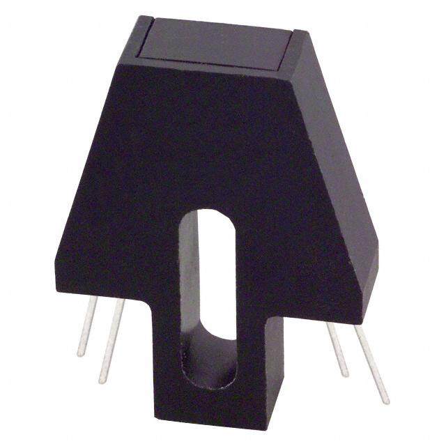
ICGOO电子元器件商城为您提供QRD1114由Fairchild Semiconductor设计生产,在icgoo商城现货销售,并且可以通过原厂、代理商等渠道进行代购。 QRD1114价格参考。Fairchild SemiconductorQRD1114封装/规格:光学传感器 - 反射式 - 模拟输出, Reflective Optical Sensor 0.050" (1.27mm) Radial - 4 Leads。您可以下载QRD1114参考资料、Datasheet数据手册功能说明书,资料中有QRD1114 详细功能的应用电路图电压和使用方法及教程。
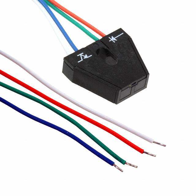
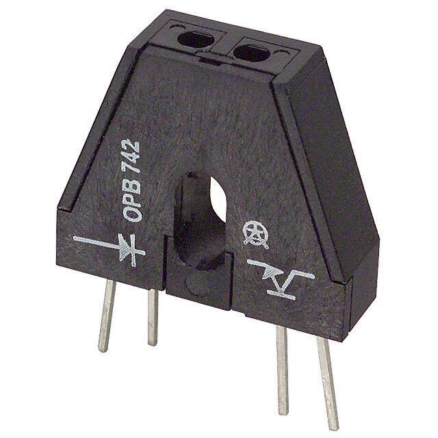
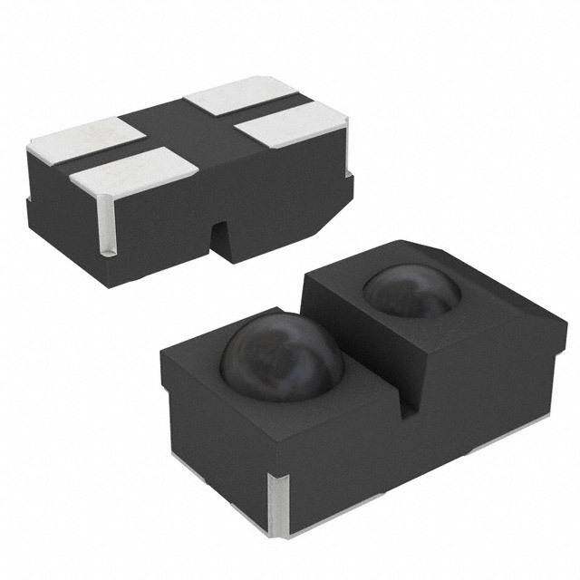
ON Semiconductor的QRD1114是一款反射式光学传感器,具有模拟输出特性。它主要应用于需要检测物体存在、位置或运动的场景中。以下是该型号的具体应用场景:

 1. 接近检测
QRD1114常用于检测物体是否靠近传感器。例如,在自动门系统中,当有人或物体接近时,传感器会检测到反射光的变化,并触发门的开启或关闭动作。它也可以用于家电设备,如冰箱门的开关检测,确保门关闭时内部密封良好。

 2. 液位检测
在液体容器中,QRD1114可以用来检测液位高度。通过将传感器安装在容器的侧面或底部,当液体达到一定高度时,光线会被液体反射回传感器,从而触发相应的信号。这种应用常见于打印机墨盒、洗衣机水位检测等场合。

 3. 物体计数
QRD1114可用于生产线上的物体计数。当物体经过传感器时,反射光的变化会被记录下来,从而实现对通过物体的数量进行精确统计。这种应用广泛用于自动化生产线、包装机械等领域。

 4. 颜色识别
虽然QRD1114不是专门的颜色传感器,但它可以通过反射光强度的变化来区分不同颜色的物体。由于不同颜色的物体对光线的反射率不同,传感器可以根据反射光的强弱来判断物体的颜色。这在分拣系统中有一定的应用价值。

 5. 纸张检测
在打印机、复印机等办公设备中,QRD1114可以用于检测纸张的存在和位置。当纸张进入设备时,传感器会检测到纸张表面反射的光线变化,确保设备能够正确处理纸张,避免卡纸等问题。

 6. 按键检测
在一些家用电器或工业控制面板上,QRD1114可以用作非接触式按键检测。用户按下按钮时,手指或物体遮挡光线,传感器检测到反射光的变化并触发相应的操作。这种方式不仅提高了使用的便利性,还减少了机械磨损。

 7. 障碍物检测
在机器人或自动化设备中,QRD1114可以用于检测前方是否有障碍物。通过发射红外光并检测反射回来的光线,传感器能够及时感知障碍物的存在,帮助设备避开碰撞。

总之,QRD1114凭借其灵敏的反射式检测能力和模拟输出特性,广泛应用于各种需要非接触式检测的场景中,尤其适合对精度要求较高的工业和消费电子领域。
| 参数 | 数值 |
| 产品目录 | |
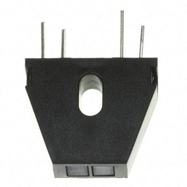
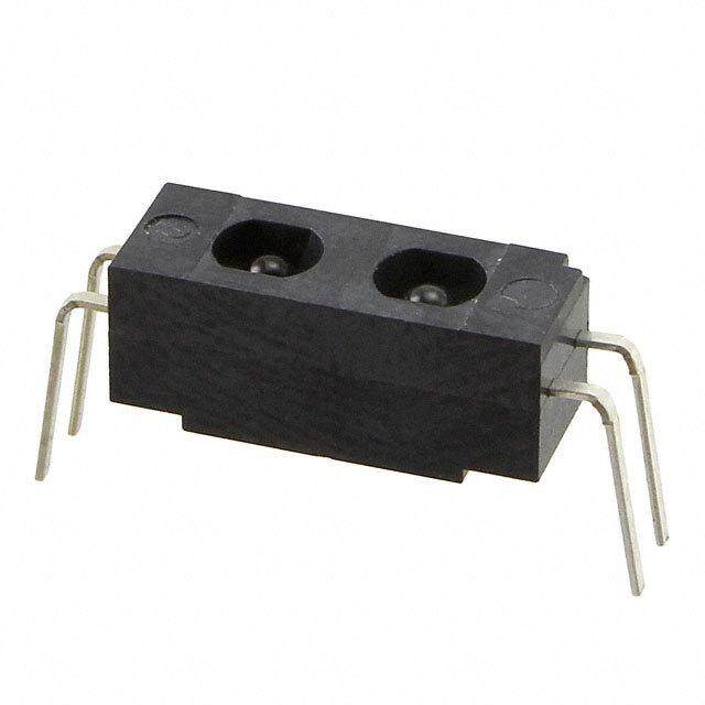
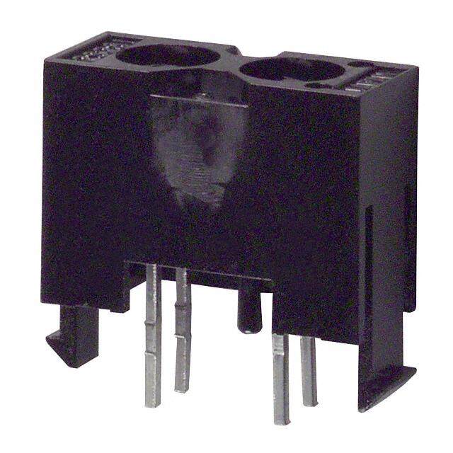
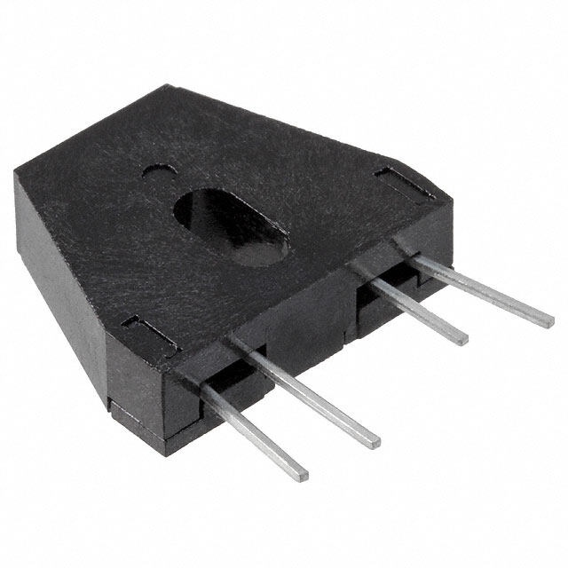
| 描述 | SENSR OPTO TRANS 1.27MM REFL PCB光学开关(反射型,光电晶体管输出) PHOTO TRANS |
| 产品分类 | |
| 品牌 | Fairchild Semiconductor |
| 产品手册 | |
| 产品图片 |
|
| rohs | 符合RoHS无铅 / 符合限制有害物质指令(RoHS)规范要求 |
| 产品系列 | 光学开关(反射型,光电晶体管输出),Fairchild Semiconductor QRD1114- |
| 数据手册 | |
| 产品型号 | QRD1114 |
| 上升时间 | 10 us |
| 下降时间 | 50 us |
| 产品目录页面 | |
| 产品种类 | 光学开关(反射型,光电晶体管输出) |
| 其它名称 | QRD1114QT |
| 包装 | 散装 |
| 反向电压 | 5 V |
| 响应时间 | 10µs, 50µs |
| 商标 | Fairchild Semiconductor |
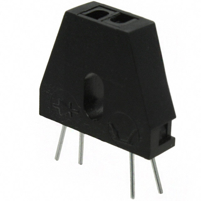
| 安装类型 | 通孔 |
| 安装风格 | Through Hole |
| 封装 | Bulk |
| 封装/外壳 | PCB 安装 |
| 工作温度 | -40°C ~ 85°C |
| 工厂包装数量 | 100 |
| 感应方式 | Reflective |
| 感应方法 | 反射 |
| 感应距离 | 0.050"(1.27mm) |
| 最大工作温度 | + 85 C |
| 最大集电极电流 | 1 mA |
| 最小工作温度 | - 40 C |
| 标准包装 | 100 |
| 正向电压 | 1.7 V |
| 正向电流 | 20 mA |
| 波长 | 940 nm |
| 电压-集射极击穿(最大值) | 30V |
| 电流-DC正向(If) | 50mA |
| 电流-集电极(Ic)(最大值) | - |
| 系列 | QRD1114 |
| 输出类型 | 光电晶体管 |
| 输出设备 | Phototransistor |
| 集电极—发射极最大电压VCEO | 30 V |
| 零件号别名 | QRD1114_NL |


- 商务部:美国ITC正式对集成电路等产品启动337调查
- 曝三星4nm工艺存在良率问题 高通将骁龙8 Gen1或转产台积电
- 太阳诱电将投资9.5亿元在常州建新厂生产MLCC 预计2023年完工
- 英特尔发布欧洲新工厂建设计划 深化IDM 2.0 战略
- 台积电先进制程称霸业界 有大客户加持明年业绩稳了
- 达到5530亿美元!SIA预计今年全球半导体销售额将创下新高
- 英特尔拟将自动驾驶子公司Mobileye上市 估值或超500亿美元
- 三星加码芯片和SET,合并消费电子和移动部门,撤换高东真等 CEO
- 三星电子宣布重大人事变动 还合并消费电子和移动部门
- 海关总署:前11个月进口集成电路产品价值2.52万亿元 增长14.8%

PDF Datasheet 数据手册内容提取
Is Now Part of To learn more about ON Semiconductor, please visit our website at www.onsemi.com Please note: As part of the Fairchild Semiconductor integration, some of the Fairchild orderable part numbers will need to change in order to meet ON Semiconductor’s system requirements. Since the ON Semiconductor product management systems do not have the ability to manage part nomenclature that utilizes an underscore (_), the underscore (_) in the Fairchild part numbers will be changed to a dash (-). This document may contain device numbers with an underscore (_). Please check the ON Semiconductor website to verify the updated device numbers. The most current and up-to-date ordering information can be found at www.onsemi.com. Please email any questions regarding the system integration to Fairchild_questions@onsemi.com. ON Semiconductor and the ON Semiconductor logo are trademarks of Semiconductor Components Industries, LLC dba ON Semiconductor or its subsidiaries in the United States and/or other countries. ON Semiconductor owns the rights to a number of patents, trademarks, copyrights, trade secrets, and other intellectual property. A listing of ON Semiconductor’s product/patent coverage may be accessed at www.onsemi.com/site/pdf/Patent-Marking.pdf. ON Semiconductor reserves the right to make changes without further notice to any products herein. ON Semiconductor makes no warranty, representation or guarantee regarding the suitability of its products for any particular purpose, nor does ON Semiconductor assume any liability arising out of the application or use of any product or circuit, and specifically disclaims any and all liability, including without limitation special, consequential or incidental damages. Buyer is responsible for its products and applications using ON Semiconductor products, including compliance with all laws, regulations and safety requirements or standards, regardless of any support or applications information provided by ON Semiconductor. “Typical” parameters which may be provided in ON Semiconductor data sheets and/or specifications can and do vary in different applications and actual performance may vary over time. All operating parameters, including “Typicals” must be validated for each customer application by customer’s technical experts. ON Semiconductor does not convey any license under its patent rights nor the rights of others. ON Semiconductor products are not designed, intended, or authorized for use as a critical component in life support systems or any FDA Class 3 medical devices or medical devices with a same or similar classification in a foreign jurisdiction or any devices intended for implantation in the human body. Should Buyer purchase or use ON Semiconductor products for any such unintended or unauthorized application, Buyer shall indemnify and hold ON Semiconductor and its officers, employees, subsidiaries, affiliates, and distributors harmless against all claims, costs, damages, and expenses, and reasonable attorney fees arising out of, directly or indirectly, any claim of personal injury or death associated with such unintended or unauthorized use, even if such claim alleges that ON Semiconductor was negligent regarding the design or manufacture of the part. ON Semiconductor is an Equal Opportunity/Affirmative Action Employer. This literature is subject to all applicable copyright laws and is not for resale in any manner.
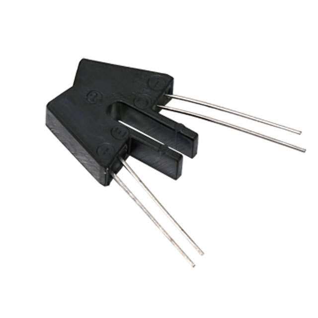
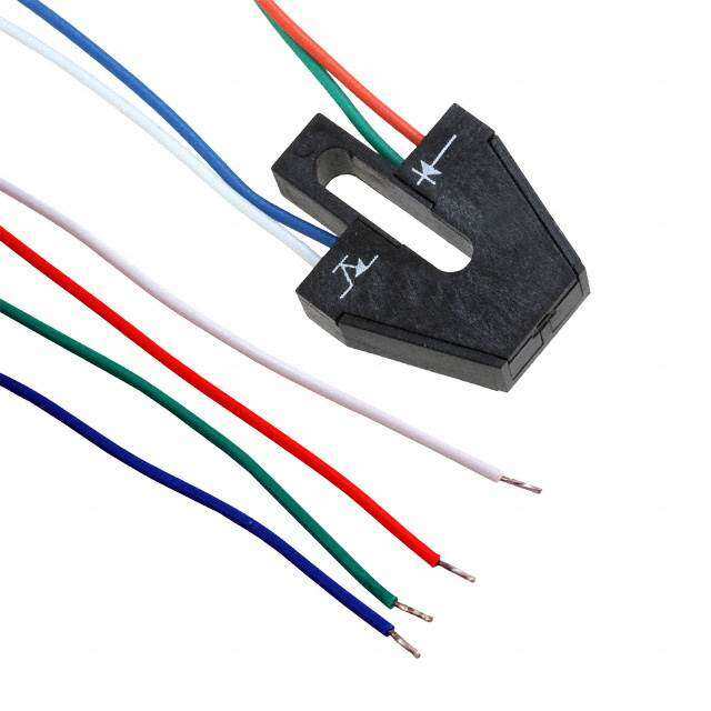
Q R D 1 June 2017 1 1 3 / Q R D QRD1113 / QRD1114 1 1 1 Reflective Object Sensor 4 — R e f l e Features Description c t i The QRD1113 and QRD1114 reflective sensors consist of v • Phototransistor Output e an infrared emitting diode and an NPN silicon phototrans- • No-Contact Surface Sensing O istor mounted side by side in a black plastic housing. The b • Unfocused for Sensing Diffused Surfaces on-axis radiation of the emitter and the on-axis response je • Compact Package of the detector are both perpendicular to the face of the c t • Daylight Filter on sensor QRD1113 and QRD1114. The phototransistor responds S to radiation emitted from the diode only when a reflective e n object or surface is in the field of view of the detector. s o r Schematic 2 3 1 4 PIN 1. Collector PIN 3. Anode PIN 2. Emitter PIN 4. Cathode Ordering Information Operating Part Number Package Top Mark Packing Method Temperature QRD1113 Custom 4L QRD1113 Bulk -40 to +85°C QRD1114 Custom 4L QRD1114 Bulk © 2005 Fairchild Semiconductor Corporation www.fairchildsemi.com QRD1113 / QRD1114 Rev. 1.3..0 1
Q R Absolute Maximum Ratings D 1 Stresses exceeding the absolute maximum ratings may damage the device. The device may not function or be opera- 1 1 ble above the recommended operating conditions and stressing the parts to these levels is not recommended. In addi- 3 tion, extended exposure to stresses above the recommended operating conditions may affect device reliability. The / absolute maximum ratings are stress ratings only. Values are at T = 25°C unless otherwise specified. Q A R Symbol Parameter Min. Unit D 1 T Operating Temperature -40 to +85 1 OPR 1 4 TSTG Storage Temperature -40 to + 100 °C — TSOL-I Lead Temperature (Solder Iron)(1,2,3) 240 for 5 s R T Lead Temperature (Solder Flow)(1,2) 260 for 10 s e SOL-F f l EMMITER e c t I Continuous Forward Current 50 mA i F v e VR Reverse Voltage 5 V O P Power Dissipation 100 mW b D j e SEMSOR c t VCEO Collector-Emitter Voltage 30 V S e V Emitter-Collector Voltage V n ECO s P Power Dissipation(4) 100 mW o D r Notes: 1.RMA flux is recommended. 2.Methanol or isopropyl alcohols are recommended as cleaning agents. 3.Soldering iron tip 1/16 inch (1.6 mm) minimum from housing. 4.Derate power dissipation linearly 1.33 mW/°C. © 2005 Fairchild Semiconductor Corporation www.fairchildsemi.com QRD1113 / QRD1114 Rev. 1.3.0 2
Q R Electrical / Optical Characteristics D 1 1 Values are at T = 25°C unless specified otherwise. 1 A 3 Symbol Parameter Test Conditions Min. Typ. Max. Units / Q INPUT (Emitter) R V Forward Voltage I = 20 mA 1.7 V D F F 1 IR Reverse Leakage Current VR = 5 V 100 μA 11 λ Peak Emission Wavelength I = 20 mA 940 nm 4 PE F — OUTPUT (Sensor) R BV Collector-Emitter Breakdown I = 1 mA 30 V CEO C e f BV Emitter-Collector Breakdown I = 0.1 mA 5 V l ECO E e c ID Dark Current VCE = 10 V, IF = 0 mA 100 nA ti v COUPLED e IICC((OONN)) QQRRDD11111134 CCoolllleeccttoorr CCuurrrreenntt IDF == 02.00 5m0A i,n VchC(E5 , =7 )5 V, 0.3100 mmAA Obje I = 40 mA, I = 100 μA, c VCE(SAT) Collector Emitter Saturation Voltage DF = 0.050 incCh(5, 7) 0.4 V t S e ICX Cross Talk IEF = = 2 00( 6m)A, VCE =5 V, 0.2 10.0 μA ns E o tr Rise Time VCE = 5 V, RL = 100 Ω, 10 μs r tf Fall time IC(ON) = 5 mA 50 μs Notes: 5.D is the distance from the sensor face to the reflective surface. 6.Crosstalk (I ) is the collector current measured with the indicated current on the input diode and with no reflective CK surface. 7.Measured using Eastman Kodak natural white test card with 90% diffused reflecting as a reflecting surface. © 2005 Fairchild Semiconductor Corporation www.fairchildsemi.com QRD1113 / QRD1114 Rev. 1.3.0 3
Q R Typical Performance Characteristics D 1 1 1 3 / Q R D 1 1 1 4 — R e f l e 0.80 c t i v e O b j e c t S e n s o r Figure 1. Forward Voltage vs. Forward Current Figure 2. Normalized Collector Current vs. Forward Current Figure 3. Normalized Collector Current vs. Figure 4. Normalized Collector Dark Current vs. Temperature Temperature © 2005 Fairchild Semiconductor Corporation www.fairchildsemi.com QRD1113 / QRD1114 Rev. 1.3.0 4
Q R Typical Performance Characteristics (continued) D 1 1 1 3 / Q R D 1 1 1 4 — R e f l e c t i v e O b j e c t S e n s o r Figure 5. Normalized Collector Current vs. Distance © 2005 Fairchild Semiconductor Corporation www.fairchildsemi.com QRD1113 / QRD1114 Rev. 1.3.0 5
Q R Physical Dimensions D 1 1 1 3 / Custom 4L Q R D 1 1 1 4 0.083 (2.11) PIN 1 INDICATOR — OPTICAL R e CENTERLINE f l e c 0.240 (6.10) ti v 0.120 (3.05) e O b j 0.173 (4.39) e c t S e 0.183 (4.65) n s o r 0.500 (12.7) MIN 0.020 (0.51) SQ. (4X) 2 3 0.100 (2.54) 1 4 0.083 (2.11) Notes: 1.Dimensions for all drawings are in inches (millimeters). 2.Tolerance of ± .010 (.25) on all non-nominal dimensions unless otherwise specified. 3.Pins 2 and 4 typically .050" shorter than pins 1 and 3. 4.Dimensions controlled at housing surface. Figure 6. REFLECTIVE RECTANGULAR SENSOR PCB MOUNT (ACTIVE) Package drawings are provided as a service to customers considering Fairchild components. Drawings may change in any manner without notice. Please note the revision and/or date on the drawing and contact a Fairchild Semiconductor representative to verify or obtain the most recent revision. Package specifications do not expand the terms of Fairchild’s worldwide terms and conditions, specifically the warranty therein, which covers Fairchild products. Always visit Fairchild Semiconductor’s online packaging area for the most recent package drawings: http://www.fairchildsemi.com/packaging/. For current tape and reel specifications, visit Fairchild Semiconductor’s online packaging area: http://www.fairchildsemi.com/packing_dwg/PKG-ARU311A-LOCZ.pdf. © 2005 Fairchild Semiconductor Corporation www.fairchildsemi.com QRD1113 / QRD1114 Rev. 1.3.0 6
ON Semiconductor and are trademarks of Semiconductor Components Industries, LLC dba ON Semiconductor or its subsidiaries in the United States and/or other countries. ON Semiconductor owns the rights to a number of patents, trademarks, copyrights, trade secrets, and other intellectual property. A listing of ON Semiconductor’s product/patent coverage may be accessed at www.onsemi.com/site/pdf/Patent−Marking.pdf. ON Semiconductor reserves the right to make changes without further notice to any products herein. ON Semiconductor makes no warranty, representation or guarantee regarding the suitability of its products for any particular purpose, nor does ON Semiconductor assume any liability arising out of the application or use of any product or circuit, and specifically disclaims any and all liability, including without limitation special, consequential or incidental damages. Buyer is responsible for its products and applications using ON Semiconductor products, including compliance with all laws, regulations and safety requirements or standards, regardless of any support or applications information provided by ON Semiconductor. “Typical” parameters which may be provided in ON Semiconductor data sheets and/or specifications can and do vary in different applications and actual performance may vary over time. All operating parameters, including “Typicals” must be validated for each customer application by customer’s technical experts. ON Semiconductor does not convey any license under its patent rights nor the rights of others. ON Semiconductor products are not designed, intended, or authorized for use as a critical component in life support systems or any FDA Class 3 medical devices or medical devices with a same or similar classification in a foreign jurisdiction or any devices intended for implantation in the human body. Should Buyer purchase or use ON Semiconductor products for any such unintended or unauthorized application, Buyer shall indemnify and hold ON Semiconductor and its officers, employees, subsidiaries, affiliates, and distributors harmless against all claims, costs, damages, and expenses, and reasonable attorney fees arising out of, directly or indirectly, any claim of personal injury or death associated with such unintended or unauthorized use, even if such claim alleges that ON Semiconductor was negligent regarding the design or manufacture of the part. ON Semiconductor is an Equal Opportunity/Affirmative Action Employer. This literature is subject to all applicable copyright laws and is not for resale in any manner. PUBLICATION ORDERING INFORMATION LITERATURE FULFILLMENT: N. American Technical Support: 800−282−9855 Toll Free ON Semiconductor Website: www.onsemi.com Literature Distribution Center for ON Semiconductor USA/Canada 19521 E. 32nd Pkwy, Aurora, Colorado 80011 USA Europe, Middle East and Africa Technical Support: Order Literature: http://www.onsemi.com/orderlit Phone: 303−675−2175 or 800−344−3860 Toll Free USA/Canada Phone: 421 33 790 2910 Fax: 303−675−2176 or 800−344−3867 Toll Free USA/Canada Japan Customer Focus Center For additional information, please contact your local Email: orderlit@onsemi.com Phone: 81−3−5817−1050 Sales Representative © Semiconductor Components Industries, LLC www.onsemi.com www.onsemi.com 1
Mouser Electronics Authorized Distributor Click to View Pricing, Inventory, Delivery & Lifecycle Information: O N Semiconductor: QRD1114