ICGOO在线商城 > PXF60-24S12

 Datasheet下载
- 型号: PXF60-24S12
- 制造商: TDK-LAMBDA CORPORATION
- 库位|库存: xxxx|xxxx
- 要求:
| 数量阶梯 | 香港交货 | 国内含税 |
| +xxxx | $xxxx | ¥xxxx |
查看当月历史价格
查看今年历史价格
PXF60-24S12产品简介:
ICGOO电子元器件商城为您提供PXF60-24S12由TDK-LAMBDA CORPORATION设计生产,在icgoo商城现货销售,并且可以通过原厂、代理商等渠道进行代购。 提供PXF60-24S12价格参考以及TDK-LAMBDA CORPORATIONPXF60-24S12封装/规格参数等产品信息。 你可以下载PXF60-24S12参考资料、Datasheet数据手册功能说明书, 资料中有PXF60-24S12详细功能的应用电路图电压和使用方法及教程。
| 参数 | 数值 |
| 产品目录 | |
| 描述 | DC-DC CONVERTER 12V 5A SGL OUT |
| 产品分类 | DC DC Converters |
| 品牌 | TDK-Lambda Americas Inc |
| 数据手册 | |
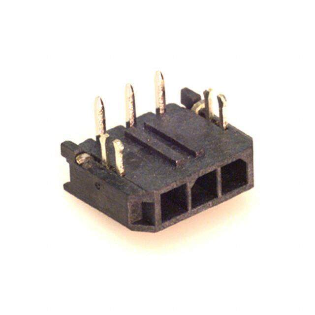
| 产品图片 |
|
| 产品型号 | PXF60-24S12 |
| rohs | 无铅 / 符合限制有害物质指令(RoHS)规范要求 |
| 产品系列 | PXF |
| 产品目录页面 | |
| 其它名称 | 285-1989 |
| 功率(W)-制造系列 | 60W |
| 功率(W)-最大值 | 60W |
| 包装 | 管件 |
| 大小/尺寸 | 2.00" 长 x 2.00" 宽 x 0.40" 高(50.8mm x 50.8mm x 10.2mm) |
| 安装类型 | 通孔 |
| 封装/外壳 | 10-DIP 模块(8 引线) |
| 工作温度 | - |
| 效率 | 90% |
| 标准包装 | 1 |
| 特性 | 远程开/关,OCP,OVP,SCP |
| 特色产品 | http://www.digikey.com/cn/zh/ph/TDK/PXF.html |
| 电压-输入(最大值) | 36V |
| 电压-输入(最小值) | 18V |
| 电压-输出1 | 12V |
| 电压-输出2 | - |
| 电压-输出3 | - |
| 电压-隔离 | 1.6kV(1600V) |
| 电流-输出(最大值) | 5A |
| 类型 | 隔离模块 |
| 输出数 | 1 |


- 商务部:美国ITC正式对集成电路等产品启动337调查
- 曝三星4nm工艺存在良率问题 高通将骁龙8 Gen1或转产台积电
- 太阳诱电将投资9.5亿元在常州建新厂生产MLCC 预计2023年完工
- 英特尔发布欧洲新工厂建设计划 深化IDM 2.0 战略
- 台积电先进制程称霸业界 有大客户加持明年业绩稳了
- 达到5530亿美元!SIA预计今年全球半导体销售额将创下新高
- 英特尔拟将自动驾驶子公司Mobileye上市 估值或超500亿美元
- 三星加码芯片和SET,合并消费电子和移动部门,撤换高东真等 CEO
- 三星电子宣布重大人事变动 还合并消费电子和移动部门
- 海关总署:前11个月进口集成电路产品价值2.52万亿元 增长14.8%


PDF Datasheet 数据手册内容提取
PXF60-Single Output DC/DC Converter 18 to 36 Vdc and 36 to 75 Vdc input, 3.3 to 15 Vdc Single Output, 60W Features Single output current up to 14A 60 watts maximum output power 2:1 wide input voltage range of 18-36 and 36-75VDC Six-sided continuous shield Case grounding ` High efficiency up to 90% Low profile:2.002.000.40 inches (50.850.810.2 mm ) Fixed switching frequency RoHS directive compliant Input to output isolation: 1600Vdc,min Over-temperature protection Input under-voltage protection Output over-voltage protection Over-current protection, auto-recovery Output short circuit protection, auto-recovery Remote ON/OFF Applications Options Distributed power architectures Heat sinks available for extended operation Workstations Remote ON/OFF logic configuration Computer equipment Communications equipment General Description The PXF60-xxSxx single output series offers 60 watts of output power from a 2.00 x 2.00 x 0.4 inch package. This series has a 2:1 wide input voltage of 18-36VDC and 36-75VDC , features 1600VDC of isolation, short-circuit and over-voltage protection, and six sided shielding. Table of Contents Absolute Maximum Ratings P2 Heat Sink Consideration P25 Output Specification P2 Remote ON/OFF Control P26 Input Specification P3 Mechanical Data P27 General Specification P4 Recommended Pad Layout P27 Characteristic Curves P5 Output Voltage Adjustment P28 Test Configurations P21 Remote Sense Application Circuit P29 EMC Considerations P22 Soldering Considerations P29 Input Source Impedance P24 Packaging Information P30 Output Over Current Protection P24 Part Number Structure P30 Output Over Voltage Protection P24 Safety and Installation Instruction P31 Thermal Consideration P25 MTBF and Reliability P31
Mar. 06, 2019 60W, Single Output Absolute Maximum Rating Parameter Model Min Max Unit Input Voltage Continuous 24Sxx 36 48Sxx 75 Vdc Transient (100ms) 24Sxx 50 48Sxx 100 Operating Ambient Temperature (With Derating) All -40 110 °C Operating Case Temperature All 110 °C Storage Temperature All -55 125 °C Output Specification Parameter Model Min Typ Max Unit Output Voltage xxS3P3 3.267 3.3 3.333 (Vin = Vin(nom) ; Full Load ; TA=25°C) xxS05 4.95 5 5.05 VDC xxS12 11.88 12 12.12 xxS15 14.85 15 15.15 Voltage Adjustability All -10 +10 % Output Regulation Line (Vin(min) to Vin(max) at Full Load) All -0.2 +0.2 % Load (0% to 100% of Full Load) -0.5 +0.5 Output Ripple & Noise xxS3P3 75 Peak-to-Peak (5Hz to 20MHz Bandwidth) xxS05 75 mVp-p xxS12 100 xxS15 100 Temperature Coefficient All -0.02 +0.02 %/°C Output Voltage Overshoot All 0 3 % VO (Vin = Vin(min) to Vin(max) ; Full Load ; TA=25°C) Dynamic Load Response (Vin = Vin(nom) ; TA=25°C) Load Step Change From 75% to 100% or 100 to 75% of Full Load Peak Deviation All 200 mV Setting Time (Vo<10% Peak Deviation) All 250 μS Output Current xxS3P3 0 14000 xxS05 0 12000 mA xxS12 0 5000 xxS15 0 4000 Output Over Voltage Protection xxS3P3 3.7 5.4 (Voltage Clamped) xxS05 5.6 7.0 Vdc xxS12 13.8 17.5 xxS15 16.8 20.5 Output Over Current Protection All 150 % FL. Output Short Circuit Protection All Hiccup, Automatic Recovery VER:00 Page 2 of 31 Issued Date:2009/03/02
Mar. 06, 2019 60W, Single Output Input Specification Parameter Model Min Typ Max Unit Operating Input Voltage 24Sxx 18 24 36 Vdc 48Sxx 36 48 75 Input Current 24S3P3 2264 (Maximum Value at Vin = Vin(nom); Full Load) 24S05 2941 24S12 2907 24S15 2907 mA 48S3P3 1132 48S05 1453 48S12 1453 48S15 1453 Input Standby Current 24S3P3 100 (Typical Value at Vin = Vin(nom); No Load) 24S05 130 24S12 150 24S15 150 mA 48S3P3 80 48S05 90 48S12 100 48S15 100 Under Voltage Lockout Turn-on Threshold 24Sxx 17 Vdc 48Sxx 34 Under Voltage Lockout Turn-off Threshold 24Sxx 15 Vdc 48Sxx 32 Input Reflected Ripple Current All 20 mAp-p (5 to 20MHz, 12μH Source Impedance) Start Up Time (Vin = Vin(nom) and Constant Resistive Load) All ms Power Up 20 Remote ON/OFF 20 Remote ON/OFF Control Vdc (The ON/OFF pin voltage is referenced to -V ) IN All Positive Logic DC-DC ON(Open) 3 12 DC-DC OFF(Short) 0 1.2 Remote Off Input Current ALL 4 mA Input Current of Remote Control Pin ALL -0.5 1 mA VER:00 Page 3 of 31 Issued Date:2009/03/02
Mar. 06, 2019 60W, Single Output General Specification Parameter Model Min Typ Max Unit Efficiency 24S3P3 89.0 (Vin = Vin(nom) ; Full Load ; TA=25°C) 24S05 90.0 24S12 90.0 24S15 90.0 % 48S3P3 89.0 48S05 90.0 48S12 90.0 48S15 90.0 Isolation Voltage Input to Output All 1600 Vdc Input to Case, Output to Case Isolation Resistance All 1 GΩ Isolation Capacitance All 1500 pF Switching Frequency All 300 KHz Weight All 60.0 g MTBF Bellcore TR-NWT-000332, TC=40°C All 1.093×10⁶ hours MIL-HDBK-217F 1.096×10⁵ VER:00 Page 4 of 31 Issued Date:2009/03/02
Mar. 06, 2019 60W, Single Output Characteristic Curves All test conditions are at 25°C.The figures are for PXF60-24S3P3 Efficiency Versus Output Current Power Dissipation Versus Output Current Efficiency Versus Input Voltage. Full Load Derating Output Current Versus Ambient Temperature and Airflow Vin = Vin(nom) Derating Output Current Versus Ambient Temperature with Heat-Sink and Airflow Vin = Vin(nom) VER:00 Page 5 of 31 Issued Date:2009/03/02
Mar. 06, 2019 60W, Single Output Characteristic Curves (Continued) All test conditions are at 25°C.The figures are for PXF60-24S3P3 Typical Output Ripple and Noise. Transient Response to Dynamic Load Change from Vin = Vin(nom), Full Load 100% to 75% to 100% of Full Load ; Vin = Vin(nom) Typical Input Start-Up and Output Rise Characteristic Using ON/OFF Voltage Start-Up and Vo Rise Characteristic Vin = Vin(nom), Full Load Vin = Vin(nom), Full Load Conduction Emission of EN55022 Class A Conduction Emission of EN55022 Class B Vin = Vin(nom), Full Load Vin = Vin(nom), Full Load VER:00 Page 6 of 31 Issued Date:2009/03/02
Mar. 06, 2019 60W, Single Output Characteristic Curves (Continued) All test conditions are at 25°C.The figures are for PXF60-24S05 Efficiency Versus Output Current Power Dissipation Versus Output Current Efficiency Versus Input Voltage. Full Load Derating Output Current Versus Ambient Temperature and Airflow Vin=Vin(nom) Derating Output Current Versus Ambient Temperature with Heat-Sink and Airflow Vin = Vin(nom) VER:00 Page 7 of 31 Issued Date:2009/03/02
Mar. 06, 2019 60W, Single Output Characteristic Curves (Continued) All test conditions are at 25°C.The figures are for PXF60-24S05 Typical Output Ripple and Noise. Transient Response to Dynamic Load Change from Vin=Vin(nom), Full Load 100% to 75% to 100% of Full Load ; Vin=Vin(nom) Typical Input Start-Up and Output Rise Characteristic Using ON/OFF Voltage Start-Up and Vo Rise Characteristic Vin=Vin(nom), Full Load Vin=Vin(nom), Full Load Conduction Emission of EN55022 Class A Conduction Emission of EN55022 Class B Vin=Vin(nom), Full Load Vin=Vin(nom), Full Load VER:00 Page 8 of 31 Issued Date:2009/03/02
Mar. 06, 2019 60W, Single Output Characteristic Curves (Continued) All test conditions are at 25°C.The figures are for PXF60-24S12 Efficiency Versus Output Current Power Dissipation Versus Output Current Efficiency Versus Input Voltage. Full Load Derating Output Current Versus Ambient Temperature and Airflow Vin=Vin(nom) Derating Output Current Versus Ambient Temperature with Heat-Sink and Airflow Vin = Vin(nom) VER:00 Page 9 of 31 Issued Date:2009/03/02
Mar. 06, 2019 60W, Single Output Characteristic Curves (Continued) All test conditions are at 25°C.The figures are for PXF60-24S12 Typical Output Ripple and Noise. Transient Response to Dynamic Load Change from Vin=Vin(nom), Full Load 100% to 75% to 100% of Full Load ; Vin=Vin(nom) Typical Input Start-Up and Output Rise Characteristic Using ON/OFF Voltage Start-Up and Vo Rise Characteristic Vin=Vin(nom), Full Load Vin=Vin(nom), Full Load Conduction Emission of EN55022 Class A Conduction Emission of EN55022 Class B Vin=Vin(nom), Full Load Vin=Vin(nom), Full Load VER:00 Page 10 of 31 Issued Date:2009/03/02
Mar. 06, 2019 60W, Single Output Characteristic Curves (Continued) All test conditions are at 25°C.The figures are for PXF60-24S15 Efficiency Versus Output Current Power Dissipation Versus Output Current Efficiency Versus Input Voltage. Full Load Derating Output Current Versus Ambient Temperature and Airflow Vin=Vin(nom) Derating Output Current Versus Ambient Temperature with Heat-Sink and Airflow Vin = Vin(nom) VER:00 Page 11 of 31 Issued Date:2009/03/02
Mar. 06, 2019 60W, Single Output Characteristic Curves (Continued) All test conditions are at 25°C.The figures are for PXF60-24S15 Typical Output Ripple and Noise. Transient Response to Dynamic Load Change from Vin=Vin(nom), Full Load 100% to 75% to 100% of Full Load ; Vin=Vin(nom) Typical Input Start-Up and Output Rise Characteristic Using ON/OFF Voltage Start-Up and Vo Rise Characteristic Vin=Vin(nom), Full Load Vin=Vin(nom), Full Load Conduction Emission of EN55022 Class A Conduction Emission of EN55022 Class B Vin=Vin(nom), Full Load Vin=Vin(nom), Full Load VER:00 Page 12 of 31 Issued Date:2009/03/02
Mar. 06, 2019 60W, Single Output Characteristic Curves (Continued) All test conditions are at 25°C.The figures are for PXF60-48S3P3 Efficiency Versus Output Current Power Dissipation Versus Output Current Efficiency Versus Input Voltage. Full Load Derating Output Current Versus Ambient Temperature and Airflow Vin=Vin(nom) Derating Output Current Versus Ambient Temperature with Heat-Sink and Airflow Vin = Vin(nom) VER:00 Page 13 of 31 Issued Date:2009/03/02
Mar. 06, 2019 60W, Single Output Characteristic Curves (Continued) All test conditions are at 25°C.The figures are for PXF60-48S3P3 Typical Output Ripple and Noise. Transient Response to Dynamic Load Change from Vin=Vin(nom), Full Load 100% to 75% to 100% of Full Load ; Vin=Vin(nom) Typical Input Start-Up and Output Rise Characteristic Using ON/OFF Voltage Start-Up and Vo Rise Characteristic Vin=Vin(nom), Full Load Vin=Vin(nom), Full Load Conduction Emission of EN55022 Class A Conduction Emission of EN55022 Class B Vin=Vin(nom), Full Load Vin=Vin(nom), Full Load VER:00 Page 14 of 31 Issued Date:2009/03/02
Mar. 06, 2019 60W, Single Output Characteristic Curves (Continued) All test conditions are at 25°C.The figures are for PXF60-48S05 Efficiency Versus Output Current Power Dissipation Versus Output Current Efficiency Versus Input Voltage. Full Load Derating Output Current Versus Ambient Temperature and Airflow Vin=Vin(nom) Derating Output Current Versus Ambient Temperature with Heat-Sink and Airflow Vin = Vin(nom) VER:00 Page 15 of 31 Issued Date:2009/03/02
Mar. 06, 2019 60W, Single Output Characteristic Curves (Continued) All test conditions are at 25°C.The figures are for PXF60-48S05 Typical Output Ripple and Noise. Transient Response to Dynamic Load Change from Vin=Vin(nom), Full Load 100% to 75% to 100% of Full Load ; Vin=Vin(nom) Typical Input Start-Up and Output Rise Characteristic Using ON/OFF Voltage Start-Up and Vo Rise Characteristic Vin=Vin(nom), Full Load Vin=Vin(nom), Full Load Conduction Emission of EN55022 Class A Conduction Emission of EN55022 Class B Vin=Vin(nom), Full Load Vin=Vin(nom), Full Load VER:00 Page 16 of 31 Issued Date:2009/03/02
Mar. 06, 2019 60W, Single Output Characteristic Curves (Continued) All test conditions are at 25°C.The figures are for PXF60-48S12 Efficiency Versus Output Current Power Dissipation Versus Output Current Efficiency Versus Input Voltage. Full Load Derating Output Current Versus Ambient Temperature and Airflow Vin=Vin(nom) Derating Output Current Versus Ambient Temperature with Heat-Sink and Airflow Vin = Vin(nom) VER:00 Page 17 of 31 Issued Date:2009/03/02
Mar. 06, 2019 60W, Single Output Characteristic Curves (Continued) All test conditions are at 25°C.The figures are for PXF60-48S12 Typical Output Ripple and Noise. Transient Response to Dynamic Load Change from Vin=Vin(nom), Full Load 100% to 75% to 100% of Full Load ; Vin=Vin(nom) Typical Input Start-Up and Output Rise Characteristic Using ON/OFF Voltage Start-Up and Vo Rise Characteristic Vin=Vin(nom), Full Load Vin=Vin(nom), Full Load Conduction Emission of EN55022 Class A Conduction Emission of EN55022 Class B Vin=Vin(nom), Full Load Vin=Vin(nom), Full Load VER:00 Page 18 of 31 Issued Date:2009/03/02
Mar. 06, 2019 60W, Single Output Characteristic Curves (Continued) All test conditions are at 25°C.The figures are for PXF60-48S15 Efficiency Versus Output Current Power Dissipation Versus Output Current Efficiency Versus Input Voltage. Full Load Derating Output Current Versus Ambient Temperature and Airflow Vin=Vin(nom) Derating Output Current Versus Ambient Temperature with Heat-Sink and Airflow Vin = Vin(nom) VER:00 Page 19 of 31 Issued Date:2009/03/02
Mar. 06, 2019 60W, Single Output Characteristic Curves (Continued) All test conditions are at 25°C.The figures are for PXF60-48S15 Typical Output Ripple and Noise. Transient Response to Dynamic Load Change from Vin=Vin(nom), Full Load 100% to 75% to 100% of Full Load ; Vin=Vin(nom) Typical Input Start-Up and Output Rise Characteristic Using ON/OFF Voltage Start-Up and Vo Rise Characteristic Vin=Vin(nom), Full Load Vin=Vin(nom), Full Load Conduction Emission of EN55022 Class A Conduction Emission of EN55022 Class B Vin=Vin(nom), Full Load Vin=Vin(nom), Full Load VER:00 Page 20 of 31 Issued Date:2009/03/02
Mar. 06, 2019 60W, Single Output Testing Configurations Input reflected-ripple current measurement test Component Value Voltage Reference L 12μH ---- ---- C 47μF 100V Aluminum Electrolytic Capacitor Peak-to-peak output ripple & noise measurement test Output voltage and efficiency measurement test Note: All measurements are taken at the module terminals. V I Efficiency o o 100% Vin Iin VER:00 Page 21 of 31 Issued Date:2009/03/02
Mar. 06, 2019 60W, Single Output EMC considerations Suggested Schematic for EN55022 Conducted Emission Class A Limits Recommended Layout with Input Filter To meet conducted emissions EN55022 CLASS A needed the following components: PXF60-24Sxx Component Value Voltage Reference C2 6.8uF 50V 1812 MLCC C3,C4 1000pF 2KV 1808MLCC PXF60-48Sxx Component Value Voltage Reference C1,C2 2.2uF 100V 1812 MLCC C3,C4 1000pF 2KV 1808 MLCC VER:00 Page 22 of 31 Issued Date:2009/03/02
Mar. 06, 2019 60W, Single Output EMC considerations (Continued) Suggested Schematic for EN55022 Conducted Emission Class B Limits Recommended Layout with Input Filter VER:00 Page 23 of 31 Issued Date:2009/03/02
Mar. 06, 2019 60W, Single Output EMC considerations (Continued) To meet conducted emissions EN55022 CLASS B needed the following components: PXF60-24Sxx Component Value Voltage Reference C1,C3 4.7uF 50V 1812 MLCC C5,C6 1000pF 2KV 1808 MLCC L1 450uH ---- PXF60-48Sxx Component Value Voltage Reference C1,C2,C3 2.2uF 100V 1812 MLCC C5,C6 1000pF 2KV 1808MLCC L1 830uH ---- This Common Choke L1 has been defined as follow: ■ L: 450μH±35% / DCR: 25mΩ, max A height: 9.8 mm, Max ■ L: 830μH±35% / DCR: 31mΩ, max A height: 8.8mm, Max ■Test condition: 100KHz / 100mV ■ Recommended through hole: Φ0.8mm ■ All dimensions in millimeters Input Source Impedance The converter should be connected to a low impedance input source. A highly inductive source impedance can affect the stability of the converter. An input external L-C filter is recommended to minimize input reflected ripple current. The inductor has a simulated source impedance of 12μH and the capacitor is Nippon chemi-con KZE series 47μF/100V. The capacitor must be located as close as possible to the input terminals of the converter for the lowest impedance. Output Over Current Protection When excessive output currents occur in the system, circuit protection is required on all converters. Normally, overload current is maintained at approximately 150 percent of rated current for PXF60 single output series. Hiccup-mode is a method of operation to protect the converter from being damaged during an over-current fault condition. It also enables the converter to restart when the fault is removed. One of the problems resulting from over current is that excessive heat may be generated in power devices; especially MOSFET and Schottky diodes and the temperature of these devices may exceed their specified limits. A protection mechanism has to be employed to prevent those power devices from being damaged. VER:00 Page 24 of 31 Issued Date:2009/03/02
Mar. 06, 2019 60W, Single Output Output Over Voltage Protection The output over-voltage protection consists of a Zener diode that monitors the output voltage on the feedback loop. If the voltage on the output terminals exceeds the over-voltage protection threshold, then the Zener diode will send a signal to the control IC to limit the output voltage. VER:00 Page 25 of 31 Issued Date:2009/03/02
Mar. 06, 2019 60W, Single Output Thermal Consideration The converter operates in a variety of thermal environments. Sufficient cooling should be provided to help ensure reliable operation of the unit. Heat is removed by conduction, convection, and radiation to the surrounding environment. Proper cooling can be verified by measuring the point as the figure below. The temperature at this location should not exceed 110°C. When operating, adequate cooling must be provided to maintain the test point temperature at or below 110°C. Although the maximum point temperature of the power modules is 110°C, limiting this temperature to a lower value will increase the reliability. Measurement shown in inches and (millimeters) TOP VIEW Heat Sink Consideration Optional heat-sink (HAPXF) and optional heat sink clip (HAPXFCLIP); two clips required when used. All dimensions in millimeters VER:00 Page 26 of 31 Issued Date:2009/03/02
Mar. 06, 2019 60W, Single Output Remote ON/OFF Control The Remote ON/OFF Pin is used to turn on and off the DC/DC converter. The user must use a switch to control the logic voltage (high or low level) of the ON / OFF pin referenced to Vi (-). The switch can be an open collector transistor, FET or Photo-Coupler that is capable of sinking up to 1 mA at low-level logic voltage. At High-level logic(ON/OFF signal maximum voltage): the allowable leakage current of the switch at 12V is 0.5 mA. Remote ON/OFF Implementation Circuits Isolated-Control Remote ON/OFF Level Control Using TTL Output Level Control Using Line Voltage Positive Logic: PXF60 module is turned off at PXF60 module is turned on at Low-level logic High-level logic VER:00 Page 27 of 31 Issued Date:2009/03/02
Mar. 06, 2019 60W, Single Output Mechanical Data 2.00 (50.8) DIA. 0.04 (1.0) 1.10 (27.9) 0.40 (10.2) 0.20 (5.1) 0.40(10.2) 3 2 1 BOTTOM 2.00(50.8) VIEW 1.80 (45.7) 8 7 6 5 4 0.10 (2.5) 2.5) 0.22 (5.6) 0.30 (7.6) 0 ( 1 0. 0.60 (15.2) 0.20 (5.1) 1. All dimensions in Inches (mm) Tolerance: X.XX±0.02 (X.X±0.5) 0.80 (20.3) 2. Pin pitch tolerance ±0.014(0.35) PIN CONNECTION EXTERNAL OUTPUT TRIMMING PIN FUNCTION Output can be externally trimmed by 1 +INPUT using the method shown below. 2 -INPUT 3 CTRL TRIM UP TRIM DOWN 4 -SENSE 4 8 5 +SENSE 6 +OUTPUT RU RD 7 -OUTPUT 8 5 8 TRIM Recommended Pad Layout VER:00 Page 28 of 31 Issued Date:2009/03/02
Mar. 06, 2019 60W, Single Output Output Voltage Adjustment Output voltage set point adjustment allows the user to increase or decrease the output voltage set point of a module. This is accomplished by connecting an external resistor between the TRIM pin and either the SENSE(+) or SENSE(-) pins. With an external resistor between the TRIM and SENSE(-) pin, the output voltage set point increases. With an external resistor between the TRIM and SENSE(+) pin, the output voltage set point decreases. TRIM UP TRIM DOWN 4 8 R R U D 8 5 TRIM TABLE PXF60-xxS3P3 Trim up (%) 1 2 3 4 5 6 7 8 9 10 V (Volts)= 3.333 3.366 3.399 3.432 3.465 3.498 3.531 3.564 3.597 3.630 OUT R (K Ohms)= 57.930 26.165 15.577 10.283 7.106 4.988 3.476 2.341 1.459 0.753 U Trim down (%) 1 2 3 4 5 6 7 8 9 10 V (Volts)= 3.267 3.234 3.201 3.168 3.135 3.102 3.069 3.036 3.003 2.970 OUT R (K Ohms)= 69.470 31.235 18.490 12.117 8.294 5.745 3.924 2.559 1.497 0.647 D PXF60-xxS05 Trim up (%) 1 2 3 4 5 6 7 8 9 10 V (Volts)= 5.050 5.100 5.150 5.200 5.250 5.300 5.350 5.400 5.450 5.500 OUT R (K Ohms)= 36.570 16.580 9.917 6.585 4.586 3.253 2.302 1.588 1.032 0.588 U Trim down (%) 1 2 3 4 5 6 7 8 9 10 V (Volts)= 4.950 4.900 4.850 4.800 4.750 4.700 4.650 4.600 4.550 4.500 OUT R (K Ohms)= 45.533 20.612 12.306 8.152 5.660 3.999 2.812 1.922 1.230 0.676 D PXF60-xxS12 Trim up (%) 1 2 3 4 5 6 7 8 9 10 V (Volts)= 12.120 12.240 12.360 12.480 12.600 12.720 12.840 12.960 13.080 13.200 OUT R (K Ohms)= 367.910 165.950 98.636 64.977 44.782 31.318 21.701 14.488 8.879 4.391 U Trim down (%) 1 2 3 4 5 6 7 8 9 10 V (Volts)= 11.880 11.760 11.640 11.520 11.400 11.280 11.160 11.040 10.920 10.800 OUT R (K Ohms)= 460.990 207.950 123.600 81.423 56.118 39.249 27.199 18.162 11.132 5.509 D PXF60-xxS15 Trim up (%) 1 2 3 4 5 6 7 8 9 10 V (Volts)= 15.150 15.300 15.450 15.600 15.750 15.900 16.050 16.200 16.350 16.500 OUT R (K Ohms)= 404.180 180.590 106.060 68.796 46.437 31.531 20.883 12.898 6.687 1.718 U Trim down (%) 1 2 3 4 5 6 7 8 9 10 V (Volts)= 14.850 14.700 14.550 14.400 14.250 14.100 13.950 13.800 13.650 13.500 OUT R (K Ohms)= 499.820 223.410 131.270 85.204 57.563 39.136 25.974 16.102 8.424 2.282 D VER:00 Page 29 of 31 Issued Date:2009/03/02
Mar. 06, 2019 60W, Single Output Remote Sense Application Circuit The Remote Sense function can be used to regulate the voltage at the load. The Remote Sense voltage range can’t be greater than 10% Vo, i.e.: [Vo (+) to Vo (-)] – [Sense (+) to Sense (-)] ≦ 10% Vo If the Remote Sense function is not used,, connect the SENSE (+) to OUTPUT (+) and connect the SENSE (-) to OUTPUT(-) of the PXF60 converter. Operation Output Voltage with Sense Function Used Soldering Considerations Lead free wave solder profile for PXF60 Zone Reference Parameter Preheat zone Rise temp. speed : 3°C / sec max. Preheat temp. : 100~130°C Actual heating Peak temp. : 250~260°C Peak time (T1+T2 time) : 4~6 sec Reference Solder : Sn-Ag-Cu ; Sn-Cu Hand Welding : Soldering iron : Power 90W Welding Time : 2~4 sec VER:00 Page 30 of 31 Issued Date:2009/03/02
Mar. 06, 2019 60W, Single Output Temp. : 380~400°C Packaging Information 10 PCS per TUBE Part Number Structure PXF 60 – 48 S 05 Max. Output Power 60Watts Input Voltage Range Output Voltage 24 : 18 ~ 36V 3P3 : 3.3Vdc 48 : 36 ~ 75V 05 : 5Vdc 12 : 12Vdc Single Output 15 : 15Vdc Model Input Output OutputCurrent InputCurrent Eff (2) Number Range Voltage Max. Load Full Load(1) (%) PXF60-24S3P3 18 – 36 VDC 3.3 VDC 14000mA 2264mA 89 PXF60-24S05 18 – 36 VDC 5 VDC 12000mA 2941mA 90 PXF60-24S12 18 – 36 VDC 12 VDC 5000mA 2907mA 90 PXF60-24S15 18 – 36 VDC 15 VDC 4000mA 2907mA 90 PXF60-48S3P3 36 – 75 VDC 3.3 VDC 14000mA 1132mA 89 PXF60-48S05 36 – 75 VDC 5 VDC 12000mA 1453mA 90 PXF60-48S12 36 – 75 VDC 12 VDC 5000mA 1453mA 90 PXF60-48S15 36 – 75 VDC 15 VDC 4000mA 1453mA 90 Note 1. Maximum value at nominal input voltage and full load of standard type. Note 2. Typical value at nominal input voltage and full load. VER:00 Page 31 of 31 Issued Date:2009/03/02
Mar. 06, 2019 60W, Single Output Safety and Installation Instruction Fusing Consideration Caution: This converter is not internally fused. An input line fuse must always be used. This converter can be used in a wide variety of applications, ranging from simple stand-alone operation to an integrated part of a sophisticated power architecture. For maximum flexibility, internal fusing is not included; however, to achieve maximum safety and system protection, always use an input line fuse. The safety agencies require a slow-blow fuse with maximum rating of 5A for PXF60-24Sxx modules and 3A for PXF60-48Sxx modules. Based on the information provided in this data sheet on Inrush energy and maximum DC input current; the same type of fuse with lower rating can be used. Refer to the fuse manufacturer’s data for further information. MTBF and Reliability The MTBF of PXF60-SERIES of DC/DC converters has been calculated using Bellcore TR-NWT-000332 Case I: 50% stress, Operating temperature at 40 °C (Ground fixed and controlled environment ). The resulting figure for MTBF is 1.093×10⁶ hours. MIL-HDBK-217F NOTICE2 FULL LOAD, Operating temperature at 25°C. The resulting figure for MTBF is 1.096×10⁵ hours. VER:00 Page 32 of 31 Issued Date:2009/03/02