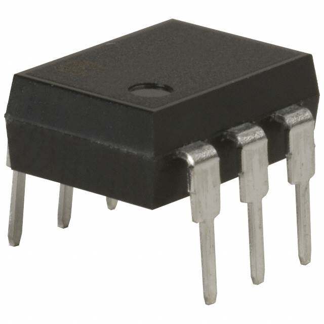
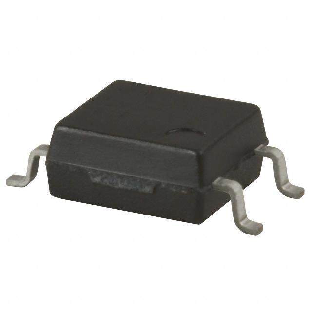
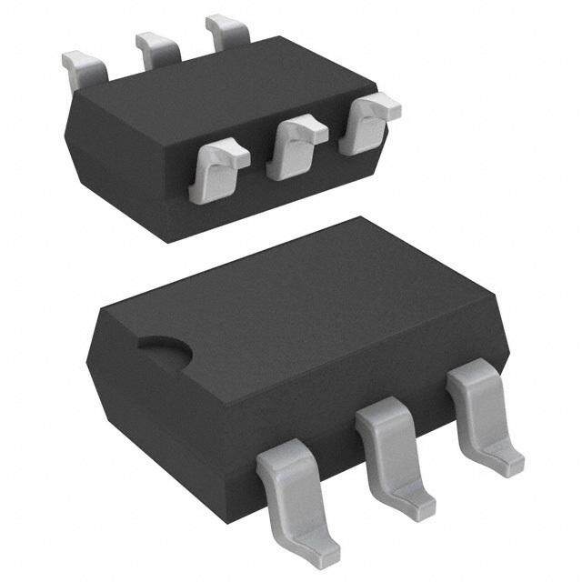
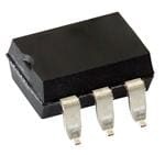
- 型号: PVN012SPBF
- 制造商: International Rectifier
- 库位|库存: xxxx|xxxx
- 要求:
| 数量阶梯 | 香港交货 | 国内含税 |
| +xxxx | $xxxx | ¥xxxx |
查看当月历史价格
查看今年历史价格
PVN012SPBF产品简介:
ICGOO电子元器件商城为您提供PVN012SPBF由International Rectifier设计生产,在icgoo商城现货销售,并且可以通过原厂、代理商等渠道进行代购。 PVN012SPBF价格参考。International RectifierPVN012SPBF封装/规格:固态继电器, 固体继电器 继电器 SPST-NO(1 Form A) 6-SMD(0.300",7.62mm)。您可以下载PVN012SPBF参考资料、Datasheet数据手册功能说明书,资料中有PVN012SPBF 详细功能的应用电路图电压和使用方法及教程。
| 参数 | 数值 |
| 产品目录 | |
| 描述 | IC RELAY PHOTOVO 20V 2.5A 6-SMD固态继电器-PCB安装 20V 1 FORM A PHOTO VOLTAIC RELAY |
| 产品分类 | |
| 品牌 | International Rectifier |
| 产品手册 | |
| 产品图片 |
|
| rohs | 符合RoHS无铅 / 符合限制有害物质指令(RoHS)规范要求 |
| 产品系列 | 固态继电器,固态继电器-PCB安装,International Rectifier PVN012SPBFPVN, HEXFET® |
| 数据手册 | |
| 产品型号 | PVN012SPBF |
| PCN组件/产地 | |
| 产品 | PCB Mount |
| 产品培训模块 | http://www.digikey.cn/PTM/IndividualPTM.page?site=cn&lang=zhs&ptm=26250 |
| 产品目录绘图 |
|
| 产品目录页面 | |
| 产品种类 | 固态继电器-PCB安装 |
| 产品类型 | PCB Mount |
| 供应商器件封装 | 6-SMT |
| 包装 | 管件 |
| 商标 | International Rectifier |
| 安装类型 | 表面贴装 |
| 安装风格 | SMD/SMT |
| 导通电阻 | 100 毫欧 |
| 封装 | Tube |
| 封装/外壳 | 6-SMD(0.300",7.62mm) |
| 封装/箱体 | SOIC-6 |
| 工厂包装数量 | 50 |
| 标准包装 | 50 |
| 电压-负载 | 0 ~ 20 V |
| 电压-输入 | 1.2VDC |
| 电路 | SPST-NO(1 Form A) |
| 端子类型 | 鸥翼型 |
| 继电器类型 | |
| 触点形式 | 1 Form A (SPST-NO) |
| 负载电压额定值 | 20 V |
| 负载电流 | 2.5A |
| 负载电流额定值 | 4.5 A |
| 输出类型 | AC,DC |



- 商务部:美国ITC正式对集成电路等产品启动337调查
- 曝三星4nm工艺存在良率问题 高通将骁龙8 Gen1或转产台积电
- 太阳诱电将投资9.5亿元在常州建新厂生产MLCC 预计2023年完工
- 英特尔发布欧洲新工厂建设计划 深化IDM 2.0 战略
- 台积电先进制程称霸业界 有大客户加持明年业绩稳了
- 达到5530亿美元!SIA预计今年全球半导体销售额将创下新高
- 英特尔拟将自动驾驶子公司Mobileye上市 估值或超500亿美元
- 三星加码芯片和SET,合并消费电子和移动部门,撤换高东真等 CEO
- 三星电子宣布重大人事变动 还合并消费电子和移动部门
- 海关总署:前11个月进口集成电路产品价值2.52万亿元 增长14.8%
PDF Datasheet 数据手册内容提取
Series PVN012PbF Microelectronic Power IC HEXFET® Power MOSFET Photovoltaic Relay Single-Pole, Normally-Open, 0-20V, 2.5A AC / 4.5A DC General Description Features The PVN012 Series Photovoltaic Relay at 100 milliohms features the lowest possible on-state (cid:131) 100mΩ On-Resistance resistance in a miniature package — lower than a (cid:131) GenV HEXFET output comparable reed relay. (cid:131) Bounce-free operation The PVN012 is a single-pole, normally open solid- (cid:131) 2.5 - 4.5 Amp capacity state relay. It utilizes a GenerationV HEXFET output (cid:131) Linear AC/DC operation switch, driven by an integrated circuit photovoltaic (cid:131) 4,000 V I/O isolation generator of novel construction. The output switch is RMS (cid:131) Solid-State reliability controlled by radiation from a GaAlAs light emitting diode (LED) which is optically isolated from the (cid:131) UL recognized photovoltaic generator. (cid:131) ESD Tolerance: These units exceed the performance capabilities of 4000V Human Body Model electromechanical relays in life, sensitivity, stable on- 500V Machine Model resistance, miniaturization, magnetic insensitivity and ruggedness. They are ideally suited for switching high currents or low level signals without distortion or injection of electrical noise. Series PVN012 Relays are packaged in a 6-lead molded DIP package with either thru-hole or surface mount (gull-wing) terminals. They are available in standard plastic shipping tubes or on tape-and-reel. Please refer to part identification information opposite. Applications (cid:131) Portable Electronics (cid:131) Programmable Logic Controllers Part Identification (cid:131) Computers and Peripheral Devices PVN012PbF thru-hole (cid:131) Audio Equipment PVN012SPbF surface-mount (cid:131) Power Supplies and Power Distribution PVN012S-TPbF surface-mount, tape (cid:131) Instrumentation and reel (HEXFET is the registered trademark for International Rectifier Power MOSFETs) 1 www.irf.com © 2015 International Rectifier Submit Datasheet Feedback May 12, 2015
Series PVN012PbF Electrical Specifications (-40°C ≤ T ≤ +85°C unless otherwise specified) A INPUT CHARACTERISTICS Limits Units Minimum Control Current (see figure 1) 3.0 mA Maximum Control Current for Off-State Resistance @ T = +25°C 0.4 mA A Control Current Range (Caution: current limit input LED, see figure 6) 3.0 to 25 mA Maximum Reverse Voltage 6.0 V OUTPUT CHARACTERISTICS Limits Units Operating Voltage Range 0 to ±20 V(DC or AC peak) Maximum Continuous Load Current @ T=+40°C, 5mA Control (see figure 1) A A Connection 2.5 A (DC or AC) B Connection 3.0 A (DC) C Connection 4.5 A (DC) Maximum Pulsed Load Current @T=+25°C, (100 ms @ 10% duty cycle) A A Connection 6.0 A (DC or AC) Maximum On-State Resistance @T=+25°C, for 1A pulsed load, 5mA Control (see figure 4) A A Connection 100 B Connection 65 mΩ C Connection 40 Minimum Off-State Resistance @ T =+25°C, ±16V 0.16 x 10⁸ Ω A DC Maximum Turn-On Time @T=+25°C (see figure 7), for 1A, 20 V load, 5mA Control 5.0 ms A DC Maximum Turn-Off Time @T=+25°C (see figure 7), for 1A, 20 V load, 5mA Control 0.5 ms A DC Maximum Output Capacitance @ 20V (see figure 2) 300 pF DC GENERAL CHARACTERISTICS Limits Units Minimum Dielectric Strength, Input-Output 4000 VRMS Minimum Insulation Resistance, Input-Output, @T =+25°C, 50%RH, 100V 1012 Ω A DC Maximum Capacitance, Input-Output 1.0 pF Maximum Pin Soldering Temperature (10 seconds maximum) +260 Ambient Temperature Range: Operating -40 to +85 °C Storage -40 to +100 International Rectifier does not recommend the use of this product in aerospace, avionics, military or life support applications. Users of this International Rectifier product in such applications assume all risks of such use and indemnify International Rectifier against all damages resulting from such use. Connection Diagrams 2 www.irf.com © 2015 International Rectifier Submit Datasheet Feedback May 12, 2015
Series PVN012PbF 3.0 1000 ILED=5 mA "A" Connection "A" Connection 2.5 A) ILED=3 mA F) 800 urrent ( 2.0 ance (p 600 d C 1.5 acit a p o a 400 x. L 1.0 al C a c M 0.5 Typi 200 0 0 0 20 40 60 80 100 0 5 10 15 20 Ambient Temperature (deg. C) Vdd, Drain to Drain Voltage (V) Figure 1. Current Derating Curves* Figure 2. Typical Output Capacitance * Derating of ‘B’ and ‘C’ connection at +85°C will be 70% of that specified at +40°C and is linear from +40°C to +85°C. 2.5 2.5 2.0 "A" Connection C) 5 mA Control 1.5 5° 2.0 ID= 1 A A) 1.0 o 2 urrent ( 00.5 alized t 1.5 Load C --01..50 n (Norm 1.0 -1.5 d-o 0.5 -2.0 R -2.5 -0.20 -0.10 0 0.10 0.20 0 -0.25 -0.15 -0.05 0.05 0.15 0.25 -50 -25 0 25 50 75 100 125 5 mA Control @ 25°C, pulsed Ambient Temperature (deg. C) Connection "A" Voltage Drop (Vdd) Figure 3. Linearity Characteristics Figure 4. Typical Normalized On-Resistance 3 www.irf.com © 2015 International Rectifier Submit Datasheet Feedback May 11, 2015
Series PVN012PbF 20 100 ClmimAaxiUtiiTmnIgOu msNo: s tptheraoatdv 2yid5 semt acAtuerrenmitt mit 30 16 cnoont terxocl eceudreredn.t rating isg. C li g. C li e e d d I/ I 25°CD-OFFD-OFF 311..000 Input Current (mA) 182 Min. device and +85 TYPICAL Max. device and -40 4 0.3 0.1 0 -35 -15 5 25 45 65 85 105 00000 00000.....55555 11111.....00000 11111.....55555 22222.....00000 Ambient Temperature (deg. C) LED Forward Voltage Drop (Volts DC) Figure 5. Typical Normalized Off-State Figure 6. Input Characteristics Leakage (Current Controlled) 20 A) m 10 nt ( urre ILED C D toff tdly ton 90% E 5 L 10% 3 ID 0.05 0.1 0.2 0.5 1.0 2.0 5.0 tdlytontoff Delay Time (milliseconds) Figure 7. Typical Delay Times Figure 8. Delay Time Definitions 4 www.irf.com © 2015 International Rectifier Submit Datasheet Feedback May 12, 2015
Series PVN012PbF Case Outlines 01-2008 01 01-2009 01 Note: For the most current drawing please refer to IR website at: http://www.irf.com/package/ 5 www.irf.com © 2015 International Rectifier Submit Datasheet Feedback May 11, 2015
Series PVN012PbF Qualification information† Industrial Qualification level (per JEDEC JESD47I †† guidelines) PVN012PbF N/A Moisture Sensitivity PVN012SPbF MSL4 Level PVN012S-TPbF (per JEDEC J-STD-020E & JEDEC J-STD-033C ††) RoHS compliant Yes † Qualification standards can be found at International Rectifier’s web site: http://www.irf.com/product-info/reliability †† Applicable version of JEDEC standard at the time of product release Revision History Date Comments • Added Qualification Information Table on page 6 5/11/2015 • Updated data sheet with new IR corporate template IR WORLD HEADQUARTERS: 101 N. Sepulveda Blvd., El Segundo, California 90245, USA Data and specifications subject to change without notice To contact International Rectifier, please visit http://www.irf.com/whoto-call/ 6 www.irf.com © 2015 International Rectifier Submit Datasheet Feedback May 12, 2015
Mouser Electronics Authorized Distributor Click to View Pricing, Inventory, Delivery & Lifecycle Information: I nfineon: PVN012PBF PVN012S-TPBF PVN012SPBF
 Datasheet下载


