ICGOO在线商城 > 隔离器 > 光隔离器 - 晶体管,光电输出 > PVI1050NS-TPBF
 Datasheet下载
- 型号: PVI1050NS-TPBF
- 制造商: International Rectifier
- 库位|库存: xxxx|xxxx
- 要求:
| 数量阶梯 | 香港交货 | 国内含税 |
| +xxxx | $xxxx | ¥xxxx |
查看当月历史价格
查看今年历史价格
PVI1050NS-TPBF产品简介:
ICGOO电子元器件商城为您提供PVI1050NS-TPBF由International Rectifier设计生产,在icgoo商城现货销售,并且可以通过原厂、代理商等渠道进行代购。 PVI1050NS-TPBF价格参考。International RectifierPVI1050NS-TPBF封装/规格:光隔离器 - 晶体管,光电输出, 光隔离器 光电型 输出 2500Vrms 2 通道 8-SMD。您可以下载PVI1050NS-TPBF参考资料、Datasheet数据手册功能说明书,资料中有PVI1050NS-TPBF 详细功能的应用电路图电压和使用方法及教程。
| 参数 | 数值 |
| 产品目录 | |
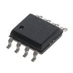
| 描述 | OPTOISO 2.5KV 2CH PHVOLT 8-SMT光电二极管输出光电耦合器 2 Form A Photo Voltaic Isolator |
| 产品分类 | |
| 品牌 | International Rectifier |
| 产品手册 | |
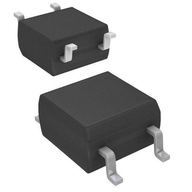
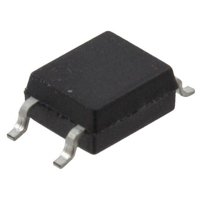
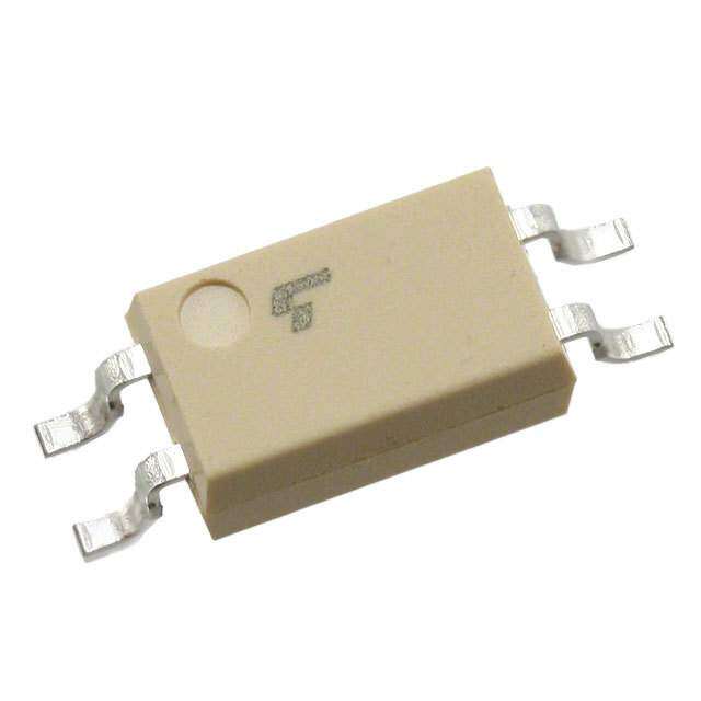
| 产品图片 |
|
| rohs | 符合RoHS无铅 / 符合限制有害物质指令(RoHS)规范要求 |
| 产品系列 | 光耦合器/光电耦合器,光电二极管输出光电耦合器,International Rectifier PVI1050NS-TPBFPVI |
| 数据手册 | |
| 产品型号 | PVI1050NS-TPBF |
| PCN组件/产地 | |
| Vce饱和值(最大值) | - |
| 上升/下降时间(典型值) | - |
| 产品培训模块 | http://www.digikey.cn/PTM/IndividualPTM.page?site=cn&lang=zhs&ptm=26250 |
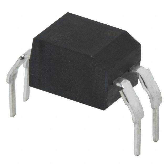
| 产品目录绘图 |
|
| 产品目录页面 | |
| 产品种类 | 光电二极管输出光电耦合器 |
| 供应商器件封装 | 8-SMD |
| 其它名称 | PVI1050NS-TPBF-ND |
| 包装 | 带卷 (TR) |
| 商标 | International Rectifier |
| 安装类型 | 表面贴装 |
| 封装 | Reel |
| 封装/外壳 | 8-SMD(4 引线),鸥翼型 |
| 封装/箱体 | SOIC-8 |
| 工作温度 | -40°C ~ 85°C |
| 工厂包装数量 | 750 |
| 打开/关闭时间(典型值) | - |
| 最大反向二极管电压 | 6 V |
| 最大工作温度 | + 85 C |
| 最大正向二极管电压 | 8 V |
| 最小工作温度 | - 40 C |
| 标准包装 | 750 |
| 正向电流 | 10 uA |
| 每芯片的通道数量 | 2 Channels |
| 电压-正向(Vf)(典型值) | - |
| 电压-输出(最大值) | 5V, 10V |
| 电压-隔离 | 2500Vrms |
| 电流-DC正向(If) | - |
| 电流-输出/通道 | - |
| 电流传输比(最大值) | - |
| 电流传输比(最小值) | - |
| 绝缘电压 | 2500 Vrms |
| 输入类型 | DC |
| 输出类型 | 光电型 |
| 输出设备 | Photovoltaic |
| 通道数 | 2 |
| 配置 | 2 Channel |


.jpg)


.jpg)

PDF Datasheet 数据手册内容提取
PVI1050NPbF PVI1050NS/TPbF PVI5050NPbF PVI5050NSPbF Photovoltaic Isolator Single and Dual Channel 5-10 Volt Output General Description The PVI Series Photovoltaic Isolator generates an electrically isolated DC voltage upon receipt of a Features DC input signal. It is capable of directly driving gates of power MOSFETs or IGBTs. It utilizes a Isolated Voltage Source monolithic integrated circuit photovoltaic generator Monolithic Construction of novel construction as its output. The output is Up to 5A Output controlled by radiation from a GaAlAs light emitting Single or Dual Output diode (LED), which is optically isolated from the Solid-State Reliability photovoltaic generator. The PVI Series is ideally suited for applications requiring high-current and/or high-voltage switching with optical isolation between the low-level driving circuitry and high-energy or high-voltage load circuits. It can be used for directly driving gates of power MOSFETs. The dual-channel device allows its outputs to drive independent discrete power MOSFETs, or be connected in parallel or in series to provide higher current drive for power MOSFETs or higher voltage drive for IGBTs. The PVI Series Photovoltaic isolators employ fast turn-off circuitry. These PVI Series Photovoltaic Isolators are packaged in 8-pin, molded DIP packages and available with either thru-hole or surface-mount (“gull-wing”) leads, in plastic shipping tubes. Part Identification Applications Load Distribution PVI1050NPbF thru-hole Industrial Controls PVI5050NPbF thru-hole Current-to-Voltage Conversion PVI1050NSPbF Surface-mount Custom Solid-State Relay (gull-wing) PVI5050NSPbF Surface-mount (gull-wing) PVI1050NS-TPbF Surface-mount, tape and reel 1 2017-12-05
PVI1050NPbF/PVI1050NS/TPbF PVI5050NPbF/PVI5050NSPbF Electrical Specifications (-40°C T +85°C unless otherwise specified) A INPUT CHARACTERISTICS Limits Units Input Current Range (see figure 4) 2.0 to 50 mA (DC) Maximum Forward Voltage Drop @ 10mA, 25°C (see figure 5) 1.4 V (DC) Maximum Reverse Voltage 6.0 V (DC) Maximum Reverse Current @ -6.0V (DC), 25°C 100 A (DC) Maximum Pulsed Input Current @ 25°C (see figure 6) 1.0 A (peak) OUTPUT CHARACTERISTICS Limits Units Maximum Forward Voltage @ 10µA 8.0 per channel V (DC) Maximum Reverse Current @ -10V 10 A DC (DC) Limits Limits COUPLED CHARACTERISTICS Units PVI5050N PVI1050N Minimum Open Circuit Voltage @ ILED = 10mA, 25°C, RL = >10M 5.0/channel 5.0 V (see figures 1 to 2) 10 series (DC) 5.0/channel Minimum Short Circuit Current @ ILED = 10mA, 25°C (see figures 1 to 2) 5.0 A 10 series (DC) Maximum Capacitance (Input/Output) 1.0 2.0 pF Maximum Ton Time @ ILED=10mA, CLOAD=10pF (See Figure7) 300 µS RL > 20M RL=10M 160 µS RL=4.7M 90 µS Maximum Toff Time @ ILED=10mA, CLOAD=10pF (See Figure7) 220 µS Limits Limits GENERAL CHARACTERISTICS Units PVI5050N PVI1050N Minimum Dielectric Strength, Input-Output 4000 2500 V RMS Minimum Dielectric Strength, Output-to-Output 1200 V DC Minimum Insulation Resistance, Input-to-Output, 1012 @T =+25°C, 50%RH, 100V A DC Maximum Pin Soldering Temperature (10 seconds maximum) +260 Ambient Temperature Range: Operating -40 to 85 °C Storage -40 to 125 Infineon Technology does not recommend the use of this product in aerospace, avionics, military or life support applications. Users of this Infineon Technology product in such applications assume all risks of such use and indemnify Infineon Technology against all damages resulting from such use. 2 2017-12-05
PVI1050NPbF/PVI1050NS/TPbF PVI5050NPbF/PVI5050NSPbF Figure 1. Typical Output Characteristics Figure 2. Typical Variation of Output Figure 3. Input Current Derating Figure 4. Input Characteristics Figure 5. Input Pulse Capability Figure 6. Typical Response Time 3 2017-12-05
PVI1050NPbF/PVI1050NS/TPbF PVI5050NPbF/PVI5050NSPbF Wiring Diagram Application Note: The outputs of the PVI1050N (pins 5-6 and 7-8) may be placed in series connection to produce a 10-volt output with a 5µA minimum short circuit current. Alternatively, the two ouptut of the PVI1050 may be connected in parallel to produce a 5.0-volt ouput with a 10µA minimum short circuit current. The two outputs of the PVI1050N may be applied separately with a maximum 1200VDC between the outputs. Input-to- output isolation to either output is 2500V (RMS). 4 2017-12-05
PVI1050NPbF/PVI1050NS/TPbF PVI5050NPbF/PVI5050NSPbF Case Outlines 5 2017-12-05
PVI1050NPbF/PVI1050NS/TPbF PVI5050NPbF/PVI5050NSPbF Case Outlines 6 2017-12-05
PVI1050NPbF/PVI1050NS/TPbF PVI5050NPbF/PVI5050NSPbF Qualifiction Information Industrial Qualification Level (per JEDEC JESD47F† guidelines) PVI1050NPbF N/A PVI5050NPbF Moisture Sensitivity Level PVI1050NSPbF MSL4 PVI5050NSPbF PVI1050NS-TPbF (per JEDEC J-STD-020E & JEDEC J-STD-033C) † RoHS Compliant Yes † Applicable version of JEDEC standard at the time of product release. 7 2017-12-05
PVI1050NPbF/PVI1050NS/TPbF PVI5050NPbF/PVI5050NSPbF Trademarks of Infineon Technologies AG µHVIC™, µIPM™, µPFC™, AU-ConvertIR™, AURIX™, C166™, CanPAK™, CIPOS™, CIPURSE™, CoolDP™, CoolGaN™, COOLiR™, CoolMOS™, CoolSET™, CoolSiC™, DAVE™, DI-POL™, DirectFET™, DrBlade™, EasyPIM™, EconoBRIDGE™, EconoDUAL™, EconoPACK™, EconoPIM™, EiceDRIVER™, eupec™, FCOS™, GaNpowIR™, HEXFET™, HITFET™, HybridPACK™, iMOTION™, IRAM™, ISOFACE™, IsoPACK™, LEDrivIR™, LITIX™, MIPAQ™, ModSTACK™, my-d™, NovalithIC™, OPTIGA™, OptiMOS™, ORIGA™, PowIRaudio™, PowIRStage™, PrimePACK™, PrimeSTACK™, PROFET™, PRO-SIL™, RASIC™, REAL3™, SmartLEWIS™, SOLID FLASH™, SPOC™, StrongIRFET™, SupIRBuck™, TEMPFET™, TRENCHSTOP™, TriCore™, UHVIC™, XHP™, XMC™ Trademarks updated November 2015 Other Trademarks All referenced product or service names and trademarks are the property of their respective owners. Edition 2016-04-19 IMPORTANT NOTICE For further information on the product, technology, The information given in this document shall in no Published by event be regarded as a guarantee of conditions or delivery terms and conditions and prices please contact your nearest Infineon Technologies office Infineon Technologies AG characteristics (“Beschaffenheitsgarantie”) . (www.infineon.com). 81726 Munich, Germany With respect to any examples, hints or any typical values stated herein and/or any information Please note that this product is not qualified © 2016 Infineon Technologies AG. regarding the application of the product, Infineon according to the AEC Q100 or AEC Q101 documents All Rights Reserved. Technologies hereby disclaims any and all of the Automotive Electronics Council. warranties and liabilities of any kind, including without limitation warranties of non-infringement Do you have a question about this of intellectual property rights of any third party. WARNINGS document? Due to technical requirements products may Email: erratum@infineon.com In addition, any information given in this contain dangerous substances. For information on document is subject to customer’s compliance the types in question please contact your nearest with its obligations stated in this document and Infineon Technologies office. any applicable legal requirements, norms and Document reference standards concerning customer’s products and Except as otherwise explicitly approved by Infineon ifx1 any use of the product of Infineon Technologies in Technologies in a written document signed by customer’s applications. authorized representatives of Infineon Technologies, Infineon Technologies’ products The data contained in this document is exclusively may not be used in any applications where a failure intended for technically trained staff. It is the of the product or any consequences of the use responsibility of customer’s technical thereof can reasonably be expected to result in departments to evaluate the suitability of the personal injury. product for the intended application and the completeness of the product information given in this document with respect to such application. 8 2017-12-05
Mouser Electronics Authorized Distributor Click to View Pricing, Inventory, Delivery & Lifecycle Information: I nfineon: PVI1050NPBF PVI1050NS-TPBF PVI5050NPBF PVI5050NSPBF PVI5080NPBF PVI5080NSPBF PVI1050NSPBF