ICGOO在线商城 > PTB78520WAH
 Datasheet下载
- 型号: PTB78520WAH
- 制造商: Texas Instruments
- 库位|库存: xxxx|xxxx
- 要求:
| 数量阶梯 | 香港交货 | 国内含税 |
| +xxxx | $xxxx | ¥xxxx |
查看当月历史价格
查看今年历史价格
PTB78520WAH产品简介:
ICGOO电子元器件商城为您提供PTB78520WAH由Texas Instruments设计生产,在icgoo商城现货销售,并且可以通过原厂、代理商等渠道进行代购。 提供PTB78520WAH价格参考以及Texas InstrumentsPTB78520WAH封装/规格参数等产品信息。 你可以下载PTB78520WAH参考资料、Datasheet数据手册功能说明书, 资料中有PTB78520WAH详细功能的应用电路图电压和使用方法及教程。
| 参数 | 数值 |
| 产品目录 | |
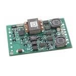
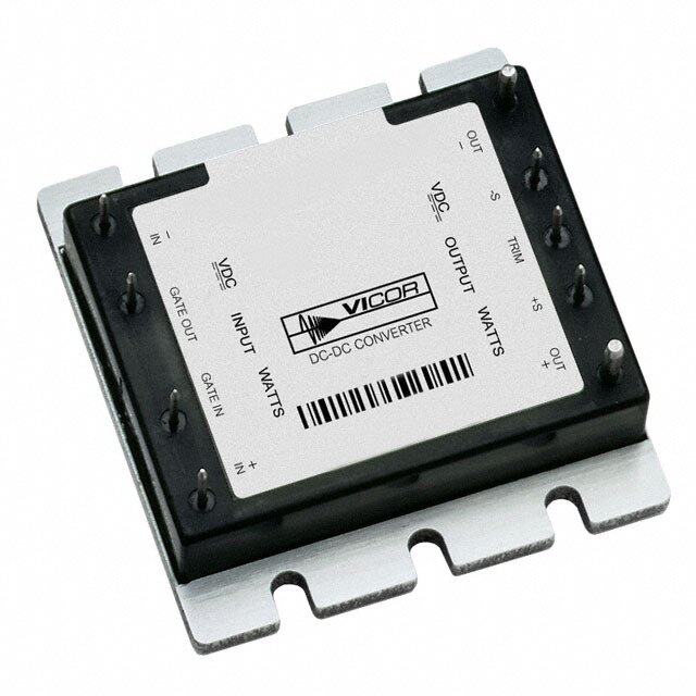
| 描述 | CONV DC/DC 1.8-3.6V 20A TH 10DIP |
| 产品分类 | DC DC Converters |
| 品牌 | Texas Instruments |
| 数据手册 | |
| 产品图片 |
|
| 产品型号 | PTB78520WAH |
| rohs | 无铅 / 符合限制有害物质指令(RoHS)规范要求 |
| 产品系列 | PTB78520W |
| 产品目录页面 | |
| 其它名称 | 296-20355 |
| 制造商产品页 | http://www.ti.com/general/docs/suppproductinfo.tsp?distId=10&orderablePartNumber=PTB78520WAH |
| 功率(W)-制造系列 | 72W |
| 功率(W)-最大值 | 72W |
| 包装 | 托盘 |
| 大小/尺寸 | 2.22" 长 x 1.45" 宽 x 0.47" 高(56.4mm x 36.8mm x 12.0mm) |
| 安装类型 | 通孔 |
| 封装/外壳 | 10-DIP 模块 |
| 工作温度 | -40°C ~ 85°C |
| 效率 | 90% |
| 标准包装 | 9 |
| 特性 | - |
| 电压-输入(最大值) | 60V |
| 电压-输入(最小值) | 18V |
| 电压-输出1 | 1.8 ~ 3.6 V |
| 电压-输出2 | - |
| 电压-输出3 | - |
| 电压-隔离 | 1.5kV(1500V) |
| 电流-输出(最大值) | 20A |
| 类型 | 隔离模块 |
| 输出数 | 1 |


- 商务部:美国ITC正式对集成电路等产品启动337调查
- 曝三星4nm工艺存在良率问题 高通将骁龙8 Gen1或转产台积电
- 太阳诱电将投资9.5亿元在常州建新厂生产MLCC 预计2023年完工
- 英特尔发布欧洲新工厂建设计划 深化IDM 2.0 战略
- 台积电先进制程称霸业界 有大客户加持明年业绩稳了
- 达到5530亿美元!SIA预计今年全球半导体销售额将创下新高
- 英特尔拟将自动驾驶子公司Mobileye上市 估值或超500亿美元
- 三星加码芯片和SET,合并消费电子和移动部门,撤换高东真等 CEO
- 三星电子宣布重大人事变动 还合并消费电子和移动部门
- 海关总署:前11个月进口集成电路产品价值2.52万亿元 增长14.8%


PDF Datasheet 数据手册内容提取
Not Recommended for New Designs PTB78520W 20-A, 18–60-V Input Auto-Track Compatible Isolated DC/DC Converter SLTS226A – JULY 2004 – REVISED OCTOBER 2005 Features • Wide-Input Voltage Range: • Auto-Track Compatible 18 V to 60 V Sequenced Output • 20 A Total Output Current • Smart-Sense Remote Sensing • 90% Efficiency • Under-voltage Lockout • Wide-Adjust Output Voltage: • Industry Standard Footprint 1.8 V to 3.6 V • Surface Mountable • Over-Current Protection • 1500 VDC Isolation • Output Over-Voltage Protection • Agency Approvals (Pending): • Over-Temperature Shutdown UL/cUL 60950, EN 60950 • Output Enable Control Description Pin-Out Information The PTB78520W is a 20-A rated, nation of input-output isolation and a Pin Function wide-input (18-60 V) isolated DC/DC wide-input voltage range, allows operation 1 +V converter that incorporates Auto-Track™ from either +24 V or –48 V. The wide- 2 V I NEnable * power-up sequencing. This allows these output adjust enables the output voltage 3 –VO IN modules to simultaneously power up with to be set to to any voltage over the range, 4 Track any other downstream non-isolated, Auto- 1.8 V to 3.6 V, using a single external 5 V Com O Track compliant module. resistor. Precise output voltage regula- 6 (–) Sense The PTB78520W module provides tion is assured using Smart-Sense. This 7 Vo Adjust two outputs, each regulated to the same is a differential remote sense that will 8 (+) Sense voltage. During power up, the voltage at intelligently regulate the sequenced out- 9 VO Bus 10 V Seq ‘V Bus’ rises first, allowing this output put, depending on its sequence status. O O to provide input power to any downstream Other operational features include an Shaded functions indicate signals non-isolated module. The voltage from input under-voltage lockout (UVLO) and electrically common with the input. ‘V Seq’ is then allowed to rise simulta- an output enable control. Over-current, *Denotes negative logic: neOously, under the control of Auto-Track, over-voltage, and over-temperature pro- Low (–OVpINen) == ONuortpmuat lo fofperation along with the outputs from the down- tection assures the module’s ability to stream modules. survive any load fault. Whether used to facilitate power-up Typical applications include distributed ™ smfeeaoqtduuuernleecs,i ntehgxe,p oePrcT toeBpd7e 8ora5ft 2eh0diWg ahs - iapn ecsrltuafondrdems- aamlnoancneey pccooommwpeprlue axtir ndcihggi iteteanclv tsuiyrrsoetnse mminse nbreotqst,uh i prtaienrlgetc ipcooumwla earrnl-yd A uSteoq- Tureancckin g DC/DC converter modules. The combi- sequencing of multiple power supply rails. Typical Application Simultaneous Powerup V1 4 Track V2 PTB78520W 8 +Sense 10 V1 =3.3 V +VI 1 VO Seq +VI 9 VO Bus 2 2VO Enable VO Adjust7 Track V2 =1.8 V 3 6 VI PTH03050WVO VO COM5 R88S7ET Inhibit GND Adjust –VI 3–VI –Sense6 C1010 µF 4 1 5R1 C1020 µF 5.49 k For technical support and further information visit http://power.ti.com
Not Recommended for New Designs PTB78520W 20-A, 18–60-V Input Auto-Track Compatible Isolated DC/DC Converter SLTS226A – JULY 2004 – REVISED OCTOBER 2005 Ordering Information Output Voltage (PTB78520❒xx) Package Options (PTB78520x❒❒) Code Voltage Code Description Pkg Ref. (1) W 1.8 V to 3.6 V AH Horiz. T/H (ERP) AS SMD, Standard (2) (ERQ) Notes: (1) Reference the applicable package reference drawing for the dimensions and PC board layout (2) “Standard” option specifies 63/37, Sn/Pb pin solder material. Pin Descriptions +V : The positive input for the module with respect to Track: The voltage at this pin directly controls the voltage IN –V . When powering the module from a negative input at the ‘V Seq’ regulated output. It is primarily used IN O voltage, this input is connected to the input source ground. to sequence the voltage at ‘V Seq’ with the regulated O outputs from any downstream non-isolated modules that –V : The negative input supply for the module, and the IN are powered from the converter’s ‘+V Bus’ output. In 0-V reference for the ‘V Enable’ input. When powering O O these applications, the ‘Track’ pin is simply connected the module from a positive source, this input is connected to the track control of each of the non-isolated mod- to the input source return. ules. The ‘Track’ pin of the PTB78520W has an internal Vo Enable*: An open-collector (open-drain) negative logic transistor, which holds it at ‘V COM’ potential for O input that is referenced to –V . This input must be pulled approximately 20 ms after the ‘V Bus’ output is in IN O to –Vin potential to enable the output voltage. A high- regulation. Following this delay, the ‘Track’ voltage and impedance connection will disable the module output. If ‘V Seq’ will rise simultaneously with the output voltage O the output enable feature is not used, pin 2 should be from all the non-isolated modules, that are under the con- permanently connected to –V . The module will then trol of Auto-Track. IN produce an output whenever a valid input source is applied. Vo Adjust: A resistor must be connected between this pin Vo Bus: Produces a positive power output with respect and ‘–Sense’ to set the converter’s output voltage. A to ‘V COM’. This is the main output from the converter 0.05-W rated resistor may be used, with tolerance and O when operated in a stand-alone configuration. It is dc- temperature stability of 1% and 100 ppm/°C, respectively. isolated from the input power pins and is the first output If this pin is left open, the converter output voltage will to rise when the converter is either powered or enabled. default to its lowest value. The specification table gives In power-up sequencing applications, this output can the preferred resistor values for the popular bus voltages. provide a 3.3-V standby source to power the downstream +Sense: The ‘+Sense’ pin can be connected to either the non-isolated modules. ‘V Bus’ or ‘V Seq’ outputs. When connected to ‘V Seq’, O O O Vo Seq: This is the sequenced output voltage from the remote sense compensation will be delayed until the converter. This voltage can be directly controlled from power-up sequence is complete. The voltage at ‘V Bus’ o the Track pin. During power up, V Seq will rise with will also be raised slightly. The pin may be left open O the Track pin voltage, typically 20 ms after the V Bus circuit, but connecting it to one of the output terminals O output has reached regulation. improves load regulation of that output. Vo COM: This is the output power return for both the –Sense: Provides the converter with a remote sense capa- ‘V Bus’ and ‘V Seq’ output voltages. This node should bility when used in conjunction with +Sense. For optimum O O be connected to the load circuit common. output voltage accuracy this pin should always be connected to ‘V COM’. This pin is also the reference connec- O tion for the output voltage set-point resistor. For technical support and further information visit http://power.ti.com
Not Recommended for New Designs PTB78520W 20-A, 18–60-V Input Auto-Track Compatible Isolated DC/DC Converter SLTS226A – JULY 2004 – REVISED OCTOBER 2005 Environmental & Absolute Maximum Ratings Characteristics Symbols Conditions Min Typ Max Units Input Voltage VIN Surge (100 ms maximum) — — 75 V Track Input Voltage VTRACK 0 — VO Bus + 0.3 V Track Input Current ITRACK (max) From external source — — 10 (i) mA Operating Temperature Range TA Over VIN Range –40 — +85 °C Over-Temperature Protection OTP PCB temperature (near pin 1) — 115 — °C Solder Reflow Temperature TREFLOW Surface temperature of module or pins — — 235 (ii) °C Storage Temperature TS — –40 — +125 °C Mechanical Shock Per Mil-STD-883D, Method 2002.3 T/H — 250 — Gs 1 msec, ½ Sine, mounted SMD — 150 — Mechanical Vibration Mil-STD-883D, Method 2007.2 T/H — 15 — Gs 20-2000 Hz, PCB mounted SMD — 5 — Weight — — 28.5 — grams Flammability — Meets UL 94V-O Notes: (i) When the Track input is fed from an external voltage source, the input current must be limited. A 2.74-kΩ value series resistor is recommended. (ii) During solder reflow of SMD package version, do not elevate the module PCB, pins, or internal component temperatures above a peak of 235 °C. Specifications (Unless otherwise stated, TA =25 °C, VIN =24 V, VO =3.3 V, CO =0 µF, and IO =IOmax) PTB78520W Characteristic Symbol Conditions Min Typ Max Units Output Current IO bus Over VIN range 0 — 20 (1) A IO seq 0 — 10 (1) (2) IO tot Sum total IO bus + IO seq 0 — 20 A Input Voltage Range VIN Over IO Range 18 48 60 V Set Point Voltage Tolerance VO tol — ±0.6 (3) — %VO Temperature Variation Regtemp –40° ≤TA ≤ +85°C — ±0.8 — %VO Line Regulation Regline Over VIN range — ±1 — mV Load Regulation Regload Over IO range — ±1 — mV Total Output Voltage Variation ∆VOtot I–n4c0l°u d≤eTs As e≤t - +p8o5in°Ct, line, load, — ±1.5 ±3 (3) %VO Output Voltage Adjust Range ∆VADJ Over Vin range 1.8 — 3.6 V Efficiency η IO =10 A RRRSSSEEETTT ===8638.597.87 Ω kk,ΩΩ,, VVVOOO ===322...305 VVV ——— 988078.5 ——— % RSET =open cct. VO =1.8 V — 86.5 — Vo Ripple (pk-pk) VR 20 MHz bandwidth — 20 — mVpp Transient Response tTR 1 A/µs load step, 50% to 100% IOmax — 75 — µs ∆VTR VO over/undershoot — ±3 — %VO Track Input (pin 4) Input Current ITRACK pin connected to VO COM — — –0.13 mA Open Circuit Voltage VTRACK 0 — VO Bus V Track Slew Rate Capability dVTRACK/dt 0.1 (4) — 1 V/ms Output Enable Input (pin 2) Referenced to –VIN (pin 3) Input High Voltage VIH 2 — open (5) V Input Low Voltage VIL –0.2 — +0.8 Input Low Current IIL — –240 — µA Standby Input Current IIN standby pin 2 open — 2 — mA No-Load Input Current IIN no-load pins 2 & 3 connected, Io TOT =0 — 85 — mA Over-Current Threshold ITRIP Shutdown, followed by auto-recovery — 30 — A Output Over-Voltage Protection OVP Output shutdown and latch off — 125 — %VO Under-Voltage Lockout UVLO 15.5 17 18 V Switching Frequency ƒS Over VIN range 225 275 325 kHz Internal Input Capacitance CIN — 3 — µF External Output Capacitance COUT Between +Vo and –Vo 0 5,000 µF Isolation Voltage Input-output & input-case 1,500 — — Vdc Capacitance Input-output — 1,000 — pF Resistance Input-output 10 — — MΩ Reliability MTBF Telcordia TR-332 1.2 — — 106 Hrs 50% stress, TA =40°C, ground benign Notes: (1) See SOA curves or consult factory for appropriate derating. (2) When load current is supplied from the VO SEQ output, the module will exhibit higher power dissipation and slightly lower operating efficiency. (3) The set-point voltage tolerance is affected by the tolerance and stability of RSET. The stated limit is unconditionally met if RSET has a tolerance of 1%, with 100 ppm/°C temperature stability. (4) When controlling the Track input from an external source the slew rate of the applied signal must be greater than the minimum limit. Failure to allow the voltage to completely rise to the voltage at the Vo Bus output, at no less than the minimum specified rate, may thermally overstress the converter. (5) The ‘VO Enable’ input has an internal pull-up, and if left open the converter output will be turned off. A discrete MOSFET or bipolar transistor is recommended to control this input. The open-circuit voltage is approximately 20% of the input voltage. If the output enable feature is not used, this pin should be permanently connected to –VIN. See application notes for other interface considerations. For technical support and further information visit http://power.ti.com
Not Recommended for New Designs Typical Characteristics PTB78520W 20-A, 18–60-V Input Auto-Track Compatible Isolated DC/DC Converter SLTS226A – JULY 2004 – REVISED OCTOBER 2005 Characteristic Data; V =24 V (See Note A) Characteristic Data; V =48 V (See Note A) IN IN Efficiency vs. Load Current (IO Bus) Efficiency vs. Load Current (IO Bus) 100 100 90 90 VOUT VOUT %) %) Efficiency - ( 7800 3221....3508VVVV Efficiency - ( 7800 3221....3508VVVV 60 60 50 50 0 4 8 12 16 20 0 4 8 12 16 20 Io Bus - (A) Io Bus - (A) Output Ripple vs. Load Current (IO Bus) Output Ripple vs. Load Current (IO Bus) 50 50 40 40 VOUT VOUT mV)30 3.3V mV)30 3.3V ple - ( 22..50VV ple - ( 22..50VV Rip20 1.8V Rip20 1.8V 10 10 0 0 0 4 8 12 16 20 0 4 8 12 16 20 Io Bus - (A) Io Bus - (A) Power Dissipation vs. Load Current (IO Bus) Power Dissipation vs. Load Current (IO Bus) 12 12 10 10 n - (W) 8 VOUT n - (W) 8 VOUT o 3.3V o 3.3V Dissipati 6 221...508VVV Dissipati 6 221...508VVV wer 4 wer 4 o o P P 2 2 0 0 0 4 8 12 16 20 0 5 10 15 20 Io Bus - (A) Io Bus - (A) Note A: All data listed in the above graphs has been developed from actual products tested at 25 °C. This data is considered typical data for the DC-DC Converter. For technical support and further information visit http://power.ti.com
Not Recommended for New Designs Typical Characteristics PTB78520W 20-A, 18–60-V Input Auto-Track Compatible Isolated DC/DC Converter SLTS226A – JULY 2004 – REVISED OCTOBER 2005 Safe Operating Areas; V =24 V (See Note B) Safe Operating Areas; V =48 V (See Note B) IN IN Load Current from ‘+VO Bus’ Output Load Current from ‘VO Bus’ Output 90 90 80 80 C) C) perature (°6700 A42ir00f00loLLwFFMM perature (°6700 A42ir00f00loLLwFFMM nt Tem50 1N0a0t LcFoMnv nt Tem50 1N0a0t LcFoMnv bie40 bie40 m m A A 30 30 20 20 0 4 8 12 16 20 0 4 8 12 16 20 Output Current (A) Output Current (A) Load Current from ‘+VO Seq’ Output Load Current from ‘VO Seq’ Output 90 90 80 80 C) C) ure (°70 Airflow ure (°70 Airflow Temperat5600 1N0a0t LcFoMnv Temperat5600 21N00a00t LLcFFoMMnv nt nt bie40 bie40 m m A A 30 30 20 20 0 2 4 6 8 10 0 2 4 6 8 10 Output Current (A) Output Current (A) Note B: SOA curves represent operating conditions at which internal components are at or below manufacturer’s maximum rated operating temperature. For technical support and further information visit http://power.ti.com
Not Recommended for New Designs Application Notes PTB78520W Operating Features and System Considerations Leaving the (+)Sense and (–)Sense pins open will not for the PTB78520W DC/DC Converter damage the converter or load circuitry. The converter includes default circuitry that keeps the output voltage in Over-Current Protection regulation. If the remote sense feature is not used, the To protect against load faults these converters incorporate (–)Sense pin should always be connected to ‘Vo COM’. output over-current protection. Applying a load to the output that exceeds the converter’s over-current threshold Note: The remote sense feature is not designed to compensate (see applicable specification) will cause the output voltage for the forward drop of non-linear or frequency dependent to momentarily fold back, and then shut down. Following components that may be placed in series with the converter shutdown the module will periodically attempt to auto- output. Examples include OR-ing diodes, filter inductors, matically recover by initiating a soft-start power-up. ferrite beads, and fuses. When these components are enclosed This is often described as a “hiccup” mode of operation, by the sense pin connections they are effectively placed inside whereby the module continues in the cycle of successive the regulation control loop, which can adversely affect the shutdown and power up until the load fault is removed. stability of the converter. Once the fault is removed, the converter automatically recovers and returns to normal operation. Over-Temperature Protection Over-temperature protection is provided by an internal Output Over-Voltage Protection temperature sensor, which monitors the temperature of The converter continually monitors for an output over- the converter’s PCB (close to pin 1). If the PCB tem- voltage (OV) condition, directly across the ‘+V Bus’ perature exceeds a nominal 115 °C, the converter will O output. The OV threshold automatically tracks the out- shut down. The converter will then automatically restart put voltage setpoint to a level that is 25% higher than when the sensed temperature drops back to approximately that set by the external R voltage adjust resistor. If 105 °C. When operated outside its recommended ther- SET the output voltage exceeds this threshold, the converter mal derating envelope (see data sheet SOA curves), the is immediately shut down and remains in a latched-off converter will typcially cycle on and off at intervals from state. To resume normal operation the converter must be a few seconds to one or two minutes. This is to ensure actively reset. This can only be done by momentarily that the internal components are not permanently dam- removing the input power to the converter. For failsafe aged from excessive thermal stress. operation and redundancy, the OV protection uses cir- cuitry that is independent of the converter’s internal Under-Voltage Lockout feedback loop. The Under-Voltage Lock-Out (UVLO) is designed to prevent the operation of the converter until the input Differential Output Voltage Sense voltage is close to the minimum operating voltage. The A differential remote sense allows a converter’s regula- converter is held off when the input voltage is below the tion circuitry to compensate for limited amounts of IR UVLO threshold, and turns on when the input voltage drop, that may be incurred between the converter and rises above the threshold. This prevents high start-up load, in either the positive or return PCB traces. Con- current during normal power-up of the converter, and necting the (+)Sense and (–)Sense pins to the respective minimizes the current drain from the input source dur- positive and ground reference of the load terminals will ing low input voltage conditions. The converter will improve the load regulation of the converter’s output meet full specifications when the minimum specified voltage at that connection point. The (–)Sense pin should input voltage is reached. The UVLO circuitry also over- always be connected to the ‘V COM’. The (+)Sense pin O rides the operation of the Vo Enable control. Only when may be connected to either the ‘+V Bus’ or ‘+V Seq’ O O the input voltage is above the UVLO threshold will the outputs. Vo Enable control be functional. When the (+)Sense pin is connected to the ‘V Seq’ O output, the voltage at ‘Vo Bus’ voltage will regulate Primary-Secondary Isolation slightly higher. Depending on the load conditions on the These converters incorporate electrical isolation between ‘V Seq’ output, the voltage at ‘V Bus’ may be up to O O the input terminals (primary) and the output terminals 100 mV higher than the converter’s set-point voltage. (secondary). All converters are tested to a withstand volt- In addition, the Smart-Sense feature (incorporated into age of 1500 VDC. This complies with UL/cUL 60950 the PTB78520 converter) will only engage sense compen- and EN 60950 and the requirements for operational isola- sation to the ‘V Seq’ output when that output voltage is O tion. It allows the converter to be configured for either a close to the set-point. During other conditions, such as positive or negative input voltage source. The data sheet power-up and power-down sequencing events, the sense ‘Pin Descriptions’ section provides guidance as to the circuit automatically defaults to sensing the ‘V Bus’ O correct reference that must be used for the external con- voltage, internal to the converter. trol signals. For technical support and further information visit http://power.ti.com
Not Recommended for New Designs Application Notes PTB78520W Output Voltage Adjustment The ‘V Adjust’ control sets the output voltages to a value O higher than 1.8 V. For output voltages other than 1.8 V a single external resistor, R , must be connected directly SET between the ‘V Adjust’ (pin 7) and ‘(–)Sense’ (pin 6) pins. O A 0.05-W rated resistor can be used. The tolerance should be 1%, with a temperature stability of 100 ppm/°C (or better). Place the resistor close to the converter and connect it directly between pins 7 & 6 using dedicated PCB traces (see typical application). Table 1-1 gives the preferred value of the external resistor for a number of standard voltages, along with the actual output voltage that this resistance value provides. For other output voltages the value of the required adjust resistor may be calculated using the following formula. R = 6.49 kΩ · 1.225 V – 4.42 kΩ SET V – 1.805 V SET Table 1-1; Preferred Values of R for Standard Output Voltages SET VSET (Standard) RSET (Pref’d Value) VSET (Actual) 3.6 V 0 Ω 3.604V 3.3 V 887 Ω 3.303 V 2.5 V 6.98 kΩ 2.503 V 2.0 V 35.7 kΩ 2.003 V 1.8 V Open 1.805 V Input Current Limiting The converter is not internally fused. For safety and overall system protection, the maximum input current to the converter must be limited. Active or passive current limiting can be used. Passive current limiting can be a fast acting fuse. A 125-V fuse, rated no more than 10 A, is recommended. Active current limiting can be imple- mented with a current limited “Hot-Swap” controller. Thermal Considerations Airflow may be necessary to ensure that the module can supply the desired load current in environments with elevated ambient temperatures. The required airflow rate may be determined from the Safe Operating Area (SOA) thermal derating chart (see converter specifica- tions). For technical support and further information visit http://power.ti.com
Not Recommended for New Designs Application Notes PTB78520W Using the Output Enable Control on the PTB78520 Figure 1-1; Output Enable Operation Auto-Track Compatible DC/DC Converter The ‘V Enable’ (pin 2) control is an active low input that Track4 O allows the output voltage from the converter to be turned PTB78520W 8 on and off while it is connected to the input source. The +Sense ‘VO Enable’ input is referenced to the –VIN (pin 3) 1, on +VIN 1+VIN VO Seq190 the primary side of the converter’s isolation, and has its VO Bus own internal pull up. The open-circuit voltage is approxi- 1 = Enable 2 7 VO Enable VO Adjust mately 20% of the applied input source voltage. L R1 QBS1S138 R8827 OA For the converter to function normally pin 2 must be 10 k 5 D pulled low to –V potential 2. The converter output will –VIN 3 VO COM6 IN –VIN –Sense then produce a regulated voltage whenever a valid source voltage is applied between +V (pin 1) and –V (pin 3) 3. IN IN If the voltage at pin 2 is allowed to rise above V (min), IH (see specification table), the output from the converter will be turned off. Turn-On Time: In the circuit of Figure 1-1, turning Q 1 off allows the voltage at pin 2 to rise to its internal pull- Figure 1-1 is an application schematic that shows the up voltage. This disables the converter output. When Q typical use of the Output Enable function. Note the discrete 1 is then turned on, it applies a low-level voltage to pin 2, transistor (Q ). Either a discrete MOSFET or bipolar 1 and enables the output of the converter. The converter transistor is recommended to control this input. Table 1-1 produces a regulated output voltage within 50 ms. Fig- gives the threshold requirements. ure 1-2 shows the output response of a PTB78520W When placed in the “Off” state the output will neither after Q is turned on. The turn on of Q corresponds to 1 1 source or sink output current. The load voltage will then the drop in the Q Vds waveform. Although the output 1 decay as the output capacitance is discharged by the load voltage rise-time is short (<10 ms), the indicated delay circuit. With the output turned off, the current drawn time (t ) will vary depending upon the input voltage and from the input source is typically reduced to 2 mA. d the module’s internal timing. The output voltage of the PTB78520W was set to 3.3 V. The waveforms were Table 1-1; Output Enable Control Requirements 1 measured with 24-Vdc input voltage, and a 10 A resistive Parameter Min Typ Max load. Enable (VIH) 2 V — — Disable (VIL) — — 0.8 V Figure 1-2; Output Enable Power-Up Characteristic VO/C [Open-Circuit] — — 13.5 V IIN [pin 1 at –VIN] — — –0.6 mA Vo Bus (1 V/Div) Notes: 1. The Output Enable control uses –V (pin 3) as its ground IN reference. All voltages are with respect to –V . IN Iin (1 A/Div) 2. Use an open-collector (or open-drain) discrete transistor to control the Output Enable input. A pull-up resistor is not necessary. To disable the converter the control pin should be pulled low to less than +0.8 V. If the Output Q Vds (5 V/Div) 1 Enable feature is not used, pin 2 should be permanently td connected to –V (pin 3). IN 3. The converter incorporates an “Under-Voltage Lockout” HORIZ SCALE: 5 ms/Div (UVLO). The UVLO does not allow the converter to power up until the input voltage is close to its minimum specified operating voltage. This is regardless of the state of the Output Enable control. Consult the specifications for the UVLO thresholds. For technical support and further information visit http://power.ti.com
Not Recommended for New Designs Application Notes PTB78520W Configuring the PTB78520 DC/DC Converter to Figure 2-1; Block Diagram of PTB78520 Auto-Track Features Power-Up Sequence with POL Modules V Bus o Overview The PTB78520 DC/DC converter has two outputs, To Smart Sense ‘V Seq’ and ‘V Bus’. ‘V Bus’ is the main output feedback (+)Sense O O O error amp’ from the converter. ‘V Seq’ is an output that is derived O from ‘VO Bus’ and can be sequenced with other supply Vo Seq voltages during power-up. Both outputs are regulated to the same set-point voltage, except that the rise in the ‘V Seq’ output is controlled by a pin called ‘Track’, and RTRK O 24.9 k delayed during power-up events. This delay allows the PTB78520W to both power and sequence with one or Track more non-isolated, 3.3-V input, Auto-Track compatible modules 1. In these applications, the PTB78520W incor- Supply 20 ms C1 TµRFK porates the necessary timing to coordinate the rise of Supervisor Delay all sequenced outputs using a common track control signal. The hold-off delay time also complies with the V COM o power-up requirements of the downstream non-isolated modules, without the need for additional components. Notes: PTB78520W Auto-Track Features 1. Auto-Track compatible modules incorporate a Track Figure 2-1 shows a block diagram of the PTB78520W input that can take direct control of the output voltage Auto-Track features. During power up, ‘V Bus’ (pin 9) during power-up transistions. The control relationship is O rises promptly, whenever the converter is connected to on a volt-for-volt basis and is active between the 0 V and a valid input source and its output is enabled. ‘V Seq’ the module’s set-point voltage. When the Track input is O (pin 10) is the Auto-Track compatible output that is derived above the set-point voltage, the module remains at its set from ‘V Bus’ but directly controlled by the voltage pre- point. Connecting the Track input of a number of such O sented at the Track input (pin 4). The control relationship modules together allows their outputs to follow a common is on a volt-for-volt basis, and is active from 0 V up to a track control voltage during power-up. voltage just below the ‘V Bus’ output. Between these two O 2. When ‘+Sense’ (pin 8) is connected to the ‘V Seq’ output O limits, the voltage at ‘V Seq’ will follow that at the ‘Track’ O (pin 10), the ‘Vo Seq’ output will be tightly regulated to input. However, once the Track input is at the ‘V Bus’ O the PTB78520W’s set-point voltage. In this configuration, voltage, raising it higher has no further effect. The volt- the voltage at the ‘V Bus’ output (pin 9) will be up to age at ‘V Seq’ cannot go higher than ‘V Bus’, and if it O O O 100 mV higher. is connected to ‘+Sense’ (pin 8), it will then regulate at the set-point voltage. 2 3 The ‘VO Seq’ output cannot sink load current. This constraint does not allow the PTB78520W to coordinate The control relationship between ‘V Seq’ and the Track O a sequenced power down. input is the same as other Auto-Track compatible outputs, across all module types. By connecting the Track input of 4. The slew rate for the Track input signal must be between the PTB78520W to the Track input of other Auto-Track 0.1 V/ms and 1 V/ms. Above this range the ‘V Seq’ O compatible modules, the output voltages can be made to output may no longer accurately follow the Track input follow a common signal during power-up transitions. 3 voltage. A slew rate below this range may thermally stress Each Track input produces a suitable track control signal the converter. These slew rate limits are met whenever the from an internal R-C time constant. An input signal can Track input voltage is allowed to rise, using the also be provided from an externally generated ramp wave- internal R-C time constants at the Track input of all form. 4, 5 modules being sequenced. The Track input of the PTB78520W has a pull-up resis- 5. Whenever an external voltage is used to control the Track tor to ‘VO Bus’, and a capacitor to ‘VO COM’. This enables input, the source current must be limited. A resistance its Track input to rise automatically; once it is allowed to value of 2.74-kΩ is recommended for this purpose. This do so. In sequencing applications, the non-isolated modules is necessary to protect the internal transistor to the are powered by the ‘VO Bus’ output. A MOSFET, internal PTB78520W converter’s Track control input. This to the PTB78520W, holds the Track voltage (and the transistor holds the track control voltage at ground ‘VO Seq’ output) at ground for 20 ms after the ‘VO Bus’ potential for 20 ms after the ‘VO Bus’ output is in output is in regulation. This gives the non-isolated mod- regulation. ules time to initialize so that their outputs can rise with the ‘V Seq’ output. O For technical support and further information visit http://power.ti.com
Not Recommended for New Designs Application Notes PTB78520W Typical Power-Up Sequencing Configuration Figure 2-2 shows how the PTB78520W (U ) can be Figure 2-3; PTB78520 Power-Up Waveforms with POL Modules 1 configured to provide two 3.3 V sources, that allow it to both power and sequence with one or more non-isolated POL modules. The example shows two PTH03050W Vo Bus (1 V/Div) modules (U & U), each rated for up 6 A of output current. 2 3 Additional voltages, as well as modules with a higher output current capability can also be specified to meet a Vo Seq (1 V/Div) specific application. The number of downstream modules, their respective output voltage and load current rating is V P O L 1 (1 V/Div) only limited by the amount of current available at the V P O L 2 (1 V/Div) ‘V Bus’ output. This is 20 A, less the current allocated O to the load circuit via the ‘V Seq’ output. O The output voltage adjust range of the PTB78520W is t d =20 ms 1.8 V to 3.6 V, which is compatible with the 3.3-V input non-isolated POL modules. In these applications, the PTB78520W output voltage must always be set to 3.3 V HORIZ SCALE: 20 ms/Div (R =887Ω). Note that this sets the output voltage of 1 both the ‘V Bus’ and ‘V Seq’ outputs. The 3.3-V input O O non-isolated modules, U and U, can be set to any volt- 2 3 stream modules to complete their power-up initialization. age over the range, 0.8 V to 2.5 V. In this example they are set to 2.5 V (R =2.21 kΩ) and 1.8 V (R =5.49 kΩ) ‘VO Seq’ (3.3 V), and the outputs VPOL1 (2.5 V) and VPOL2 2 3 (1.8 V), supply the load circuit. These three outputs respectively. Figure 2-3 shows the power-up waveforms are controlled by the track control voltage, which the from Figure 2-2 when the Track control input to all three PTB78520W holds at ground potential for 20 ms after modules are simply connected together. the ‘V Bus’ output is in regulation. When the track O The PTB78520W provides input power to the down- control voltage is finally allowed to rise, the three outputs stream non-isolated modules via the ‘Vo Bus’ output. rise simultaneously to their respective set-point voltages. This is the output that rises first to allow the down- Figure 2-2; Power-Up Sequencing Circuit With PTB78520W & Non-Isolated POL Modules U1 4 Track PTB78520W Vo Seq (3.3 V) 8 +Sense U2 2 +VI 1 VO Seq10 Track +VI 9 3 6 VPOL1 (2.5 V) VO Bus VINPTH03050WVO 2VO Enable VO Adjust7 C1 Inhib4it GND1Adju5st C1030 µF 100 µF R2 5 R1 2.21 k VO COM 887 –VI 3 6 –VI –Sense U3 2 Track 3 6 VPOL2 (1.8 V) VINPTH03050WVO Inhibit GND Adjust C4 C2 4 1 5 100 µF 100 µF R3 5.49 k For technical support and further information visit http://power.ti.com
Not Recommended for New Designs Application Notes PTB78520W Stand-Alone Operation The combination of a wide-input and wide-output volt- age range makes the PTB78520W an attractive product as a stand-alone DC/DC converter. In these applications the PTB78520W is not required to power up, or sequence with, any non-isolated POL modules. The output voltage can be adjusted to any value over the range, 1.8 V to 3.6 V, and the Auto-Track features simply disregarded. Figure 2-4 shows the the recommended configuration of the PTB78520W when it is used as a stand-alone con- verter. As a sequenced output voltage is not required, the main output, ‘V Bus’, is used to supply all the load cur- O rent. The ‘Track’ pin, and ‘V Seq’ output are simply left O open circuit. The ‘(+)Sense’ pin can also be connected to the ‘V Bus’ output for improved load regulation. O When the PTB78520W is operated in this mode, the output from ‘V Bus’ rises promptly upon power up. The O converter also exhibits slightly less power dissipation and a corresponding improvment in operating efficiency. Figure 2-4; PTB78520W Stand-Alone Configuration 4 Track PTB78520W 8 +Sense 10 1 VO Seq +VI +VI 9 VO Bus L 7 C1 O VO Adjust 100 µF A 2VO Enable RSET D 5 VO COM 3 6 –VI –VI –Sense For technical support and further information visit http://power.ti.com
PACKAGE OPTION ADDENDUM www.ti.com 19-Dec-2019 PACKAGING INFORMATION Orderable Device Status Package Type Package Pins Package Eco Plan Lead/Ball Finish MSL Peak Temp Op Temp (°C) Device Marking Samples (1) Drawing Qty (2) (6) (3) (4/5) PTB78520WAD NRND Through- ERP 10 9 RoHS (In Work) SN N / A for Pkg Type Hole Module & non-Green PTB78520WAH NRND Through- ERP 10 9 RoHS (In Work) SN N / A for Pkg Type -40 to 85 Hole Module & non-Green PTB78520WAS NRND Surface ERQ 10 9 Non-RoHS SNPB Level-1-235C-UNLIM/ -40 to 85 Mount Module & non-Green Level-3-260C-168HRS (1) The marketing status values are defined as follows: ACTIVE: Product device recommended for new designs. LIFEBUY: TI has announced that the device will be discontinued, and a lifetime-buy period is in effect. NRND: Not recommended for new designs. Device is in production to support existing customers, but TI does not recommend using this part in a new design. PREVIEW: Device has been announced but is not in production. Samples may or may not be available. OBSOLETE: TI has discontinued the production of the device. (2) RoHS: TI defines "RoHS" to mean semiconductor products that are compliant with the current EU RoHS requirements for all 10 RoHS substances, including the requirement that RoHS substance do not exceed 0.1% by weight in homogeneous materials. Where designed to be soldered at high temperatures, "RoHS" products are suitable for use in specified lead-free processes. TI may reference these types of products as "Pb-Free". RoHS Exempt: TI defines "RoHS Exempt" to mean products that contain lead but are compliant with EU RoHS pursuant to a specific EU RoHS exemption. Green: TI defines "Green" to mean the content of Chlorine (Cl) and Bromine (Br) based flame retardants meet JS709B low halogen requirements of <=1000ppm threshold. Antimony trioxide based flame retardants must also meet the <=1000ppm threshold requirement. (3) MSL, Peak Temp. - The Moisture Sensitivity Level rating according to the JEDEC industry standard classifications, and peak solder temperature. (4) There may be additional marking, which relates to the logo, the lot trace code information, or the environmental category on the device. (5) Multiple Device Markings will be inside parentheses. Only one Device Marking contained in parentheses and separated by a "~" will appear on a device. If a line is indented then it is a continuation of the previous line and the two combined represent the entire Device Marking for that device. (6) Lead/Ball Finish - Orderable Devices may have multiple material finish options. Finish options are separated by a vertical ruled line. Lead/Ball Finish values may wrap to two lines if the finish value exceeds the maximum column width. Important Information and Disclaimer:The information provided on this page represents TI's knowledge and belief as of the date that it is provided. TI bases its knowledge and belief on information provided by third parties, and makes no representation or warranty as to the accuracy of such information. Efforts are underway to better integrate information from third parties. TI has taken and continues to take reasonable steps to provide representative and accurate information but may not have conducted destructive testing or chemical analysis on incoming materials and chemicals. TI and TI suppliers consider certain information to be proprietary, and thus CAS numbers and other limited information may not be available for release. Addendum-Page 1
PACKAGE OPTION ADDENDUM www.ti.com 19-Dec-2019 In no event shall TI's liability arising out of such information exceed the total purchase price of the TI part(s) at issue in this document sold by TI to Customer on an annual basis. Addendum-Page 2
None
None
IMPORTANTNOTICEANDDISCLAIMER TIPROVIDESTECHNICALANDRELIABILITYDATA(INCLUDINGDATASHEETS),DESIGNRESOURCES(INCLUDINGREFERENCE DESIGNS),APPLICATIONOROTHERDESIGNADVICE,WEBTOOLS,SAFETYINFORMATION,ANDOTHERRESOURCES“ASIS” ANDWITHALLFAULTS,ANDDISCLAIMSALLWARRANTIES,EXPRESSANDIMPLIED,INCLUDINGWITHOUTLIMITATIONANY IMPLIEDWARRANTIESOFMERCHANTABILITY,FITNESSFORAPARTICULARPURPOSEORNON-INFRINGEMENTOFTHIRD PARTYINTELLECTUALPROPERTYRIGHTS. TheseresourcesareintendedforskilleddevelopersdesigningwithTIproducts.Youaresolelyresponsiblefor(1)selectingtheappropriate TIproductsforyourapplication,(2)designing,validatingandtestingyourapplication,and(3)ensuringyourapplicationmeetsapplicable standards,andanyothersafety,security,orotherrequirements.Theseresourcesaresubjecttochangewithoutnotice.TIgrantsyou permissiontousetheseresourcesonlyfordevelopmentofanapplicationthatusestheTIproductsdescribedintheresource.Other reproductionanddisplayoftheseresourcesisprohibited.NolicenseisgrantedtoanyotherTIintellectualpropertyrightortoanythird partyintellectualpropertyright.TIdisclaimsresponsibilityfor,andyouwillfullyindemnifyTIanditsrepresentativesagainst,anyclaims, damages,costs,losses,andliabilitiesarisingoutofyouruseoftheseresources. TI’sproductsareprovidedsubjecttoTI’sTermsofSale(www.ti.com/legal/termsofsale.html)orotherapplicabletermsavailableeitheron ti.comorprovidedinconjunctionwithsuchTIproducts.TI’sprovisionoftheseresourcesdoesnotexpandorotherwisealterTI’sapplicable warrantiesorwarrantydisclaimersforTIproducts. MailingAddress:TexasInstruments,PostOfficeBox655303,Dallas,Texas75265 Copyright©2019,TexasInstrumentsIncorporated