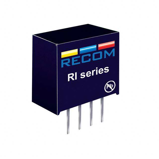
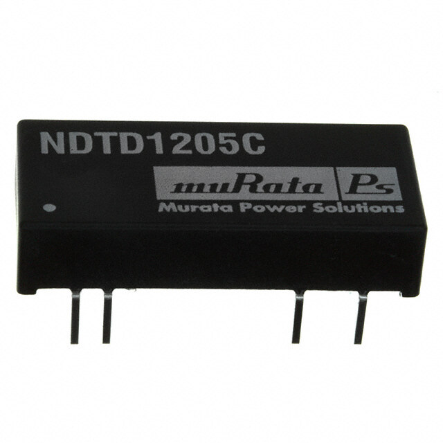
- 型号: PTB48560AAZ
- 制造商: Texas Instruments
- 库位|库存: xxxx|xxxx
- 要求:
| 数量阶梯 | 香港交货 | 国内含税 |
| +xxxx | $xxxx | ¥xxxx |
查看当月历史价格
查看今年历史价格
PTB48560AAZ产品简介:
ICGOO电子元器件商城为您提供PTB48560AAZ由Texas Instruments设计生产,在icgoo商城现货销售,并且可以通过原厂、代理商等渠道进行代购。 PTB48560AAZ价格参考。Texas InstrumentsPTB48560AAZ封装/规格:直流转换器, 隔离模块 DC/DC 转换器 1 输出 3.6 ~ 5.5 V 6A 36V - 75V 输入。您可以下载PTB48560AAZ参考资料、Datasheet数据手册功能说明书,资料中有PTB48560AAZ 详细功能的应用电路图电压和使用方法及教程。
Texas Instruments 的 PTB48560AAZ 是一款直流-直流转换器模块,属于其PTB系列的非隔离式DC/DC转换器。该模块主要面向需要高效、稳定电源转换的工业和通信设备应用。

PTB48560AAZ 输入电压范围为36V至75V,输出电压为12V,输出电流可达4.5A,具备较高的功率密度和转换效率,适合用于对空间和效率要求较高的系统。该模块内置过流、过温及欠压保护功能,提高了系统运行的可靠性。

其典型应用场景包括:

1. 通信设备:如基站电源系统、网络交换设备等,用于将-48V通信标准电源转换为适合电路使用的12V电源。
2. 工业控制系统:在PLC、工业计算机或自动化设备中,作为稳定的中间电源转换模块。
3. 测试与测量仪器:用于为内部电路提供高效、干净的电源供应。
4. 铁路与交通系统:在轨道交通设备中,为控制单元或传感器模块提供可靠电源。

该模块采用标准的½砖封装形式,兼容多种电源系统设计,便于集成与替换。
| 参数 | 数值 |
| 产品目录 | |
| 描述 | CONV DC/DC 5V 6A HZ SMD 11DIP隔离式DC/DC转换器 30-W 3.6V to 5.5V Adj DC/DC Converter |
| 产品分类 | DC DC ConvertersDC/DC转换器 |
| 品牌 | Texas Instruments |
| 产品手册 | |
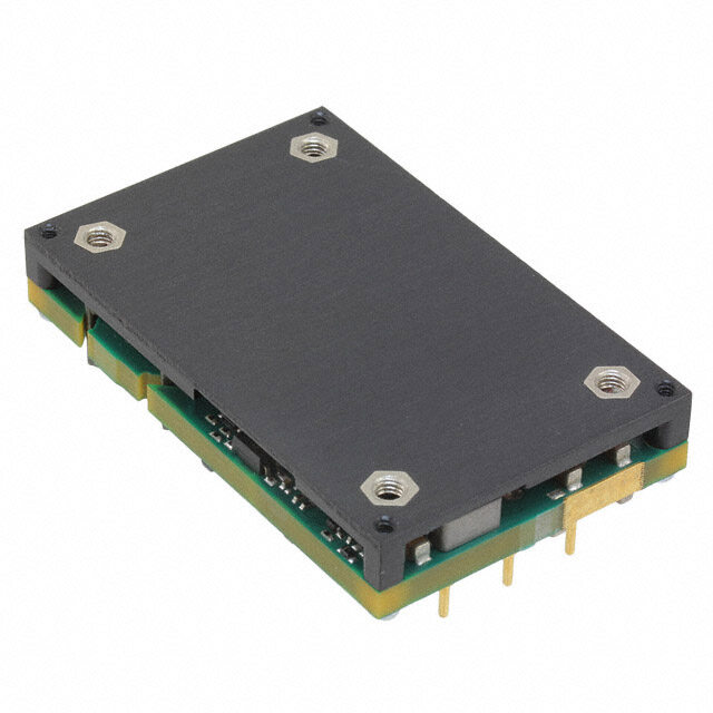
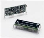
| 产品图片 |
|
| rohs | 符合RoHS无铅 / 符合限制有害物质指令(RoHS)规范要求 |
| 产品系列 | 隔离式DC/DC转换器,Texas Instruments PTB48560AAZPTB48560 |
| 数据手册 | |
| 产品型号 | PTB48560AAZ |
| 产品 | Isolated |
| 产品目录页面 | |
| 产品种类 | 隔离式DC/DC转换器 |
| 其它名称 | 296-20340 |
| 制造商产品页 | http://www.ti.com/general/docs/suppproductinfo.tsp?distId=10&orderablePartNumber=PTB48560AAZ |
| 功率(W)-制造系列 | 30W |
| 功率(W)-最大值 | 30W |
| 包装 | 托盘 |
| 商标 | Texas Instruments |
| 大小/尺寸 | 2.09" 长 x 1.09" 宽 x 0.39" 高(53.0mm x 27.6mm x 10.0mm) |
| 安装类型 | 表面贴装 |
| 安装风格 | SMD/SMT |
| 封装 | Tray |
| 封装/外壳 | 11-SMD 模块 |
| 封装/箱体尺寸 | SMD Module |
| 工作温度 | -40°C ~ 85°C |
| 工作温度范围 | - 40 C to + 85 C |
| 工厂包装数量 | 12 |
| 效率 | 84% |
| 标准包装 | 12 |
| 特性 | 远程开/关,OCP,OTP,UVLO |
| 电压-输入(最大值) | 75V |
| 电压-输入(最小值) | 36V |
| 电压-输出1 | 3.6 ~ 5.5 V |
| 电压-输出2 | - |
| 电压-输出3 | - |
| 电压-隔离 | 1.5kV(1500V) |
| 电流-输出(最大值) | 6A |
| 类型 | 隔离模块 |
| 系列 | PTB48560A |
| 输入电压范围 | 36 V to 75 V |
| 输出功率 | 30 W |
| 输出数 | 1 |
| 输出电压—通道1 | 3.6 V to 5.5 V |
| 输出电流—通道1 | 6 A |
| 输出端数量 | 1 |


- 商务部:美国ITC正式对集成电路等产品启动337调查
- 曝三星4nm工艺存在良率问题 高通将骁龙8 Gen1或转产台积电
- 太阳诱电将投资9.5亿元在常州建新厂生产MLCC 预计2023年完工
- 英特尔发布欧洲新工厂建设计划 深化IDM 2.0 战略
- 台积电先进制程称霸业界 有大客户加持明年业绩稳了
- 达到5530亿美元!SIA预计今年全球半导体销售额将创下新高
- 英特尔拟将自动驾驶子公司Mobileye上市 估值或超500亿美元
- 三星加码芯片和SET,合并消费电子和移动部门,撤换高东真等 CEO
- 三星电子宣布重大人事变动 还合并消费电子和移动部门
- 海关总署:前11个月进口集成电路产品价值2.52万亿元 增长14.8%


PDF Datasheet 数据手册内容提取
PTB48560A, PTB48560B PTB48560C www.ti.com SLTS236A–MARCH2005–REVISEDOCTOBER2005 30-W, 48-V INPUT DC/DC CONVERTERS WITH AUTO-TRACK™ SEQUENCING FEATURES APPLICATIONS • InputVoltage:36Vto 75V • IntermediateBusArchitectures • 30-W Total OutputPower • Telecom, High-End Computing Platforms • OutputVoltages:3.3V, 5V, and 12V • Multi-Rail PowerSystemswith Power-Up Sequencing • Wide-OutputAdjust/Trim • Up To 88%Efficiency • OvercurrentProtection • OvertemperatureShutdown • UndervoltageLockout • InputOvervoltageProtection • Auto-Track™Power-Up Sequencing (IncludesSequenced Outputwith PTB48560B) • Smart-SenseRemoteSensing (PTB48560B) • Dual-LogicEnableControl • Space-Saving1×2Footprint • SurfaceMountPackage • 1500-VdcIsolation • AgencyApprovals(Pending): UL/cUL 60950, EN60950 DESCRIPTION The PTB48560x is a series of 30–W rated isolated dc/dc converters, designed to operate from a standard -48–V telecom central office (CO) supply. Housed in a 1×2 package, each model has a wide-adjust output voltage that canbeset tooneof thecommonintermediatebusvoltagesof 3.3V, 5V, or12V. The PTB48560 series incorporates Auto-Track™, a feature that simplifies the power-up sequencing of multiple power modules and operates from the same intermediate bus. During a power-up cycle, modules with this feature have the capability of following a common ramp voltage applied to an input called Track. The PTB48560 series is specifically designed to control the Track voltage of any number of nonisolated downstream modules powered from its output. This ensures that the outputs of the downstream modules all rise simultaneously during power up. The PTB48560B (3.3 V) has an additional sequenced output, V Seq, which also rises with the Track O voltage. This allows the V Seq output to power up simultaneously with the outputs from other power modules O underthecontrolof Auto-Track. Whether used to facilitate power-up sequencing, or operated as a stand-alone module, the PTB48560 series includes many other features expected of high-performance dc/dc converter modules. Precise output voltage regulation is ensured with a differential remote sense. Operational features include an input undervoltage lockout (UVLO) and a dual-logic output enable control. Overcurrent and overtemperature protection ensure survival against load faults.Typical applications include distributed power architectures in both telecom and computing environments, particularly complexdigitalsystemsrequiringpowersequencingof multiplepowersupplyrails. Pleasebeawarethatanimportantnoticeconcerningavailability,standardwarranty,anduseincriticalapplicationsofTexas Instrumentssemiconductorproductsanddisclaimerstheretoappearsattheendofthisdatasheet. Auto-TrackisatrademarkofTexasInstruments. PRODUCTIONDATAinformationiscurrentasofpublicationdate. Copyright©2005,TexasInstrumentsIncorporated Products conform to specifications per the terms of the Texas Instruments standard warranty. Production processing does not necessarilyincludetestingofallparameters.
PTB48560A, PTB48560B PTB48560C www.ti.com SLTS236A–MARCH2005–REVISEDOCTOBER2005 These devices have limited built-in ESD protection. The leads should be shorted together or the device placedinconductivefoamduringstorageorhandlingtoprevent electrostaticdamagetotheMOSgates. Typical Circuit 5 Track PTB48560x V Seq(3.3V)# O +VI 1 +Sense* 9 See Note(*) +V I 11 V Seq# Track O V 1 10 Auto-Track POL VOBus VI POLModuleVO 2 PEN 8 CO‡ GND Adjust 3 VOAdjust (Required) C ‡ CO NEN I R SET 6 V COM O † -VI RSET 4 7 -VI -Sense Track V 2 POL SimultaneousPower-Up Auto-Track V V I POLModule O V Seq# O GND Adjust V 1 POL C VPOL2 CI‡ R † O SET ToOther POLModules # SequencedoutputisonlyavailablewiththePTB48560B. * The+SensecanbeconnectedtoeithertheV SeqorV BusoutputofthePTB48560B. O O † R isrequiredtosettheoutputvoltagehigherthantheminimumvalue;seetheApplicationInformationforvalues. SET ‡ ThePTB48560xmodulesrequireaminimumtotaloutputcapacitanceforproperoperation; seetheElectricalCharacterisiticsforthevaluerequiredbyeachmodel. 2
PTB48560A, PTB48560B PTB48560C www.ti.com SLTS236A–MARCH2005–REVISEDOCTOBER2005 ORDERING INFORMATION PTB48560(BasePt.Number) OutputVoltageRange PartNumber DESCRIPTION Pb–freeandRoHS PackageRef. (1) Compatible PTB48560AAH HorizontalT/H Yes ERW 3.6Vto5.5V PTB48560AAS StandardSMD (2) No ERY PTB48560AAZ OptionalSMD (3) Yes PTB48560BAH (4) HorizontalT/H Yes ERW 1.8Vto3.6V PTB48560BAS (4) StandardSMD (2) No ERY PTB48560BAZ (4) OptionalSMD (3) Yes PTB48560CAH HorizontalT/H Yes ERW 9Vtoo13.2V PTB48560CAS StandardSMD (2) No ERY PTB48560CAZ OptionalSMD (3) Yes (1) SeetheapplicablepackagereferencedrawingforthedimensionsandPCboardlayout. (2) Standardoptionspecifies63/37,Sn/Pbpinsoldermaterial. (3) Lead(Pb)–freeoptionspecifiesSn/Agpinsoldermaterial. (4) IncludesanAuto-Trackcompatibleoutput,V Seq,whichsequenceswiththeTrackcontrolduringpowerup. O ABSOLUTE MAXIMUM RATINGS PTB48560x UNIT Continuous 75 V InputVoltage I Surge,1smax 100(1) V V Trackinputvoltage 0toV Bus+0.3 (Track) O I max Trackinputcurrent Fromexternalsource 10 (2) mA (Track) T 1 Operatingtemperaturerange OverV range –40to85 A I Overtemperatureprotection PCBtemperature(nearpin1) 115 Surfacetemperatureofmodule PTB48560xAH 260(3) T Wavesoldertemperature (WAVE) orpins(5seconds) °C Surfacetemperatureofmodule PTB48560xAS 235 (3) T Solderreflowtemperature (REFLOW) orpins PTB48560xAZ 260 (3) T Storagetemperature –40to125 stg (1) Theconverter'sinternalprotectioncircuitrymaycausetheoutputtoturnoffwhentheappliedinputvoltageisgreaterthan75V. (2) WhentheTrackinputisfedfromanexternalvoltagesource,theinputcurrentmustbelimited.A2.74-kΩvalueseriesresistoris recommended. (3) DuringsolderreflowofSMDpackageversion,donotelevatethemodulePCB,pins,orinternalcomponenttemperaturesthispeak temperature. PACKAGE SPECIFICATIONS PTB48560x(SuffixesAHandAS) Weight 13.6grams Flammability MeetsUL94V-O PerMil-STD-883D,Method2002.3,1ms, HorizontalT/H(SuffixAH) 500Gs (1) Mechanicalshock 1/2Sine,mounted HorizontalSMD(SuffixAS) 250G (1) Mil-STD-883D,Method2007.2,20-2000Hz, HorizontalT/H(SuffixAH) 20G (1) Mechanicalvibration PCBmounted HorizontalSMD(SuffixAS) 5G (1) (1) Qualificationlimit. 3
PTB48560A, PTB48560B PTB48560C www.ti.com SLTS236A–MARCH2005–REVISEDOCTOBER2005 PTB48560B ELECTRICAL CHARACTERISTICS (Unlessotherwisestated,T =25°C,V =48V,V =3.3V,C =220µF,andI =I max) A I O O O O PTB48560B PARAMETER TESTCONDITIONS UNIT MIN TYP MAX OverV range I Bus 0.25 (1) 8 (2) I O I Outputcurrent I Seq 0 4 (3) A O O Sumtotal,(I Bus+I Seq) 0.25 8 O O V Inputvoltagerange OverI range 36 48 75 V I O Set-pointvoltagetolerance ±1 (4) %V O Temperaturevariation -40°C≤TA≤85°C ±0.5 %VO Lineregulation OverV range ±7 ±33 mV I V O Loadregulation OverI range ±13 ±33 mV O Totaloutputvoltagevariation Includesset-point,line,load,–40°C≤TA≤85°C ±2 ±3(4) %VO Adjustrange OverV range 1.8 3.6 V I RSET=5.36kΩ,VO=3.3V 82% η Efficiency RSET=40.2kΩ,VO=2.5V 79% R =open,V =1.8V 74% SET O V Ripple(peak-to-peak) 20-MHzbandwidth 50 mV O pp 0.1A/µsloadstep, Recoverytime 100 µs Transientresponse 50%to100% IOmax VOover/undershoot ±150 mV Inputcurrent Trackconnectedto-Sense -0.13 mA Trackinput(pin5) Open-circuitvoltage 0 V Bus O Inputslewratelimits 0.1 (5) 1 V/ms Referencedto-V Inputhighvoltage(V ) 2 Open (6) I IH V Outputenableinputs(pins2,3) Inputlowvoltage(V ) -0.2 0.8 IL Inputlowcurrent(I ) 0.48 mA IL Standbyinputcurrent Pins2and3open 8 16 mA I (tot) Overcurrentthreshold Shutdown,followedbyautorecovery 12 A O V increasing 34 I UVLO Undervoltagelockout V V decreasing 33 I ƒS Switchingfrequency OverVIrange 400 500 600 kHz Internalinputcapacitance 1 µF Externaloutputcapacitance BetweenbothoutputsandV COM 220 5,000 µF O Isolationvoltage Input-output 1,500 Vdc Isolationcapacitance Input-output 2,000 pF Isolationresistance Input-output 10 MΩ TelcordiaSR-33250%stress,T =40°C,ground MTBF Reliability A 3.6 106Hr benign (1) TheconverterrequiresaminimumloadcurrentateithertheV SeqorV Busoutputforproperoperation.Theconverterisnot O O damagedwhenoperatedunderano-loadcondition. (2) Seetemperaturederatingcurvesforsafeoperatingarea(SOA),todetermineoutputcurrentderatingatelevatedambienttemperatures. (3) WhenloadcurrentissuppliedfromtheV Seqoutput,themoduleexhibitshigherpowerdissipationandslightlyloweroperating O efficiency. (4) Theset-pointvoltagetoleranceisaffectedbythetoleranceandstabilityofR .ThestatedlimitisunconditionallymetifR hasa SET SET toleranceof1%,with100ppm/°Ctemperaturestability. (5) WhencontrollingtheTrackinputfromanexternalsource,theslewrateoftheappliedsignalmustbegreaterthantheminimumlimit. FailuretoallowthevoltagetocompletelyrisetothevoltageattheV (bus)output,atnolessthantheminimumspecifiedrate,may O thermallyoverstresstheconverter. (6) ThePENandNENinputseachhaveaninternalpullupresistor.Iftheenablefeatureisnotused,thePENinput(pin2)shouldbeleft opencircuitandtheNENinput(pin3)permanentlyconnectedto–V.AdiscreteMOSFETorbipolartransistorisrecommendedforthe I enablecontrol.Theopen-circuitvoltageislessthan10V.SeetheApplicationInformationforamoredetaileddescription. 4
PTB48560A, PTB48560B PTB48560C www.ti.com SLTS236A–MARCH2005–REVISEDOCTOBER2005 PTB48560A ELECTRICAL CHARACTERISTICS (Unlessotherwisestated,T =25°C,V =48V,V =5V,C =220µF,andI =I max) A I O O O O PTB48560A PARAMETER TESTCONDITIONS UNIT MIN TYP MAX I Outputcurrent OverV range I Bus 0.25 (1) 6 (2) A O I O V Inputvoltagerange OverI range 36 48 75 V I O Set-pointvoltagetolerance ±1 (3) %V O Temperaturevariation -40°C≤TA≤85°C ±0.5 %VO Lineregulation OverV range ±0.2 ±1 %V I O V O Loadregulation OverI range ±0.4 ±1 %V O O Totaloutputvoltagevariation Includesset-point,line,load,–40°C≤TA≤85°C ±2 ±3(3) %VO Adjustrange OverV range 3.6 5.5 V I η Efficiency RSET=14.3kΩ,VO=5V 84% V Ripple(peak-to-peak) 20-MHzbandwidth 1 %V O O 0.1A/µsloadstep, Recoverytime 100 µs Transientresponse 50%to100% IOmax VOover/undershoot ±150 mV Inputcurrent Trackconnectedto-Sense –0.2 mA Trackinput(pin5) Open-circuitvoltage 0 V Bus O Referencedto-V Inputhighvoltage(V ) 2 Open (4) I IH V Outputenableinputs(pins2,3) Inputlowvoltage(V ) -0.2 0.8 IL Inputlowcurrent(I ) 0.48 mA IL Standbyinputcurrent Pins2and3open 8 16 mA I Bus Overcurrentthreshold Shutdown,followedbyautorecovery 9 A O V increasing 34 I UVLO Undervoltagelockout V V decreasing 33 I ƒS Switchingfrequency OverVIrange 400 500 600 kHz Internalinputcapacitance 1 µF Externaloutputcapacitance BetweenbothoutputsandV COM 220 5,000 µF O Isolationvoltage Input-output 1,500 Vdc Isolationcapacitance Input-output 2,000 pF Isolationresistance Input-output 10 MΩ TelcordiaSR-33250%stress,T =40°C,ground MTBF Reliability A 3.6 106Hr benign (1) Theconverterrequiresaminimumloadcurrentforproperoperation.Theconverterisnotdamagedwhenoperatedunderano-load condition. (2) Seetemperaturederatingcurvesforsafeoperatingarea(SOA),todetermineoutputcurrentderatingatelevatedambienttemperatures. (3) Theset-pointvoltagetoleranceisaffectedbythetoleranceandstabilityofR .ThestatedlimitisunconditionallymetifR hasa SET SET toleranceof1%,with100ppm/°Ctemperaturestability. (4) ThePENandNENinputseachhaveaninternalpullupresistor.Iftheenablefeatureisnotused,thePENinput(pin2)shouldbeleft opencircuitandtheNENinput(pin3)permanentlyconnectedto–V.AdiscreteMOSFETorbipolartransistorisrecommendedforthe I enablecontrol.Theopen-circuitvoltageislessthan10V.SeetheApplicationInformationforamoredetaileddescription. 5
PTB48560A, PTB48560B PTB48560C www.ti.com SLTS236A–MARCH2005–REVISEDOCTOBER2005 PTB48560C ELECTRICAL CHARACTERISTICS (Unlessotherwisestated,T =25°C,V =48V,V =12V,C =100µF,andI =I max) A I O O O O PTB48560C PARAMETER TESTCONDITIONS UNIT MIN TYP MAX I Outputcurrent OverV range I Bus 0.1 (1) 2.5 (2) A O I O V Inputvoltagerange OverI range 36 48 75 V I O Set-pointvoltagetolerance ±1 (3) %V O Temperaturevariation -40°C≤TA≤85°C ±0.5 %VO Lineregulation OverV range ±0.2 ±1 %V I O V O Loadregulation OverI range ±0.4 ±1 %V O O Totaloutputvoltagevariation Includesset-point,line,load,–40°C≤TA≤85°C ±2 ±3(3) %VO Adjustrange OverV range 9 13.2 V I RSET=9.09kΩ,VO=12V 88% η Efficiency R =open,V = 9V 86% SET O V Ripple(peak-to-peak) 20-MHzbandwidth 1 %V O O 0.1A/µsloadstep, Recoverytime 100 µs TransientResponse 50%to100% IOmax VOover/undershoot ±150 mV Inputcurrent Trackconnectedto-Sense 0.48 mA Trackinput(pin5) Open-circuitvoltage 0 V Bus O Referencedto-V Inputhighvoltage(V ) 2 Open (4) I IH V Outputenableinputs(pins2,3) Inputlowvoltage(V ) -0.2 0.8 IL Inputlowcurrent(I ) –0.48 mA IL Standbyinputcurrent Pins2and3open 8 16 mA I Bus Overcurrentthreshold Shutdown,followedbyautorecovery 3.75 A O V increasing 34 I UVLO Undervoltagelockout V V decreasing 33 I ƒS Switchingfrequency OverVIrange 400 500 600 kHz Internalinputcapacitance 1 µF Externaloutputcapacitance BetweenbothoutputsandV COM 100 1,500 µF O Isolationvoltage Input-output 1,500 Vdc Isolationcapacitance Input-output 2,000 pF Isolationresistance Input-output 10 MΩ TelcordiaSR-33250%stress,T =40°C,ground MTBF Reliability A 3.4 106Hrs benign (1) Theconverterrequiresaminimumloadcurrentforproperoperation.Theconverterisnotdamagedwhenoperatedunderano-load condition. (2) Seetemperaturederatingcurvesforsafeoperatingarea(SOA),todetermineoutputcurrentderatingatelevatedambienttemperatures. (3) Theset-pointvoltagetoleranceisaffectedbythetoleranceandstabilityofR .ThestatedlimitisunconditionallymetifR hasa SET SET toleranceof1%,with100ppm/°Ctemperaturestability. (4) ThePENandNENenableinputseachhaveaninternalpullupresistor.Iftheenablefeatureisnotused,thePENinput(pin2)shouldbe leftopencircuitandtheNENinput(pin3)permanentlyconnectedto–V.AdiscreteMOSFETorbipolartransistorisrecommendedfor I theenablecontrol.Theopen-circuitvoltageislessthan10V.SeetheApplicationInformationforamoredetaileddescription. 6
PTB48560A, PTB48560B PTB48560C www.ti.com SLTS236A–MARCH2005–REVISEDOCTOBER2005 TERMINAL FUNCTIONS TERMINAL DESCRIPTION NAME NO. Thepositiveinputforthemodulewithrespectto-V.Whenpoweringthemodulefromanegativeinputvoltage, +V(1) 1 I I thisinputisconnectedtotheinputsourceground. Thenegativeinputsupplyforthemodule,andthe0-VreferenceforthePENandNENenableinputs.When -V(1) 4 I poweringthemodulefromapositivesource,thisinputisconnectedtotheinputsourcereturn. Anopen-collector(open-drain)positivelogicinputthatisreferencedto-V.Whenthisinputispulledto-V I I PEN (1) 2 potentialtheconverteroutputisdisabled.Thisinputmustbeopencircuitfortheconvertertooperate.The converterthenproducesanoutputwheneveravalidinputsourceisapplied. Anopen-collector(open-drain)negativelogicinputthatisreferencedto-V.Thisinputmustbepulledto-V I I potentialtoenabletheconverter.Whentheinputisopencircuit,theconverteroutputisdisabled.Iftheenable NEN (1)(2) 3 featureisnotused,thisinputshouldbepermanentlyconnectedto-V.Themodulethenproducesanoutput I wheneveravalidinputsourceisapplied. ThisisthepositivepoweroutputwithrespecttoV COM,andthemainoutputfromtheconverter.Itisdcisolated O fromtheinputpowerpinsandproducesavalidoutputvoltageapproximately20msbeforethevoltageatthe V Bus 10 O Trackterminalisallowedtorise.Thisprovidestherequiredstandbypowersourcetoanydownstreamnonisolated modulesinpower-upsequencingapplications. ThisisasequencedoutputvoltagefromtheconverterthatiscontrolledbytheTrackterminalduringpower-up transitions.ItisonlyavailabletothePTB48560B,andusedwiththeoutputvoltagesetto3.3V(anI/Osupply V Seq 11 O voltage).Duringpowerup,thevoltageatV SeqriseswiththeTrackterminal,typically20msaftertheV Bus O O outputhasreachedregulation. ThisistheoutputpowerreturnforboththeV BusandV Seqoutputvoltages.Thisterminalshouldbe V COM 6 O O O connectedtothecommonoftheloadcircuit. Thisterminalisusedinpower-upsequencingapplicationstocontroltheoutputvoltageofAuto-Trackcompatible modules,poweredfromtheconverterV Busoutput.ThisincludestheconverterV Seqoutputonthe O O PTB48560B.TheconverterTrackcontrolhasaninternaltransistor,whichholdsthevoltageclosetoV COM Track 5 O potentialforapproximately20ms(40mswiththePTB48560C)aftertheV Busoutputisinregulation.Following O thisdelay,theTrackvoltageandV Seqrisessimultaneouslywiththeoutputvoltageofallothermodules O controlledbyAuto-Track. Providestheconverterwitharemotesensecapabilitywhenusedwith+Sense.Foroptimumoutputvoltage –Sense 7 accuracy,thispinshouldalwaysbeconnectedtoV COM,closetotheloadcircuit.Thisterminalisalsothe O referenceconnectionforboththeoutputvoltageset-pointresistorandTrackcontrol. Aresistormustbeconnectedbetweenthisterminaland-Sensetosettheconverteroutputvoltage.A0.05-W ratedresistormaybeused,withtoleranceandtemperaturestabilityof1%and100ppm/°C,respectively.Ifleft V Adjust 8 O opencircuit,theconverteroutputvoltagedefaultstoitslowestvalue.Thespecificationtablegivesthestandard resistorvaluesforthemostcommonoutputvoltages. The+SensepincanbeconnectedtoV Bus(orV Seq)output.WhenconnectedtoV Seq,remotesense O O O compensationisdelayeduntiltheconverter'spower-upsequenceiscomplete.ThevoltageatV Busisalso +Sense 9 O raisedslightly.The+Senseinputmaybeleftopencircuit,butconnectingittooneoftheoutputterminalsimproves loadregulationofthatoutput. (1) Thesefunctionsindicatesignalselectricallycommonwiththeinput. (2) Denotesnegativelogic:Low(–V)=Normaloperation,Open=Outputoff I 7
PTB48560A, PTB48560B PTB48560C www.ti.com SLTS236A–MARCH2005–REVISEDOCTOBER2005 TYPICAL CHARACTERISTICS PTB48560B Characteristic Data (V = 3.3 V) (1)(2) O EFFICIENCY OUTPUTVOLTAGERIPPLE vs vs OUTPUTCURRENT OUTPUTCURRENT 90 60 VI=36V P 80 P 50 V m y-% 70 VI=60VVI=75V Ripple- 40 VI=60V VI=75V Efficienc 5600 VI=48V utVoltage 2300 utp VI=48V 40 -O 10 VI=36V O V 30 0 0 1 2 3 4 5 6 7 8 0 1 2 3 4 5 6 7 8 IO-OutputCurrent-A IO-OutputCurrent-A Figure1. Figure2. POWERDISSIPATION TEMPERATUREDERATING vs vs OUTPUTCURRENT OUTPUTCURRENT 7 90 400 LFM 6 VI=75V 80 W Dissipation- 45 VI=48VVI=60V (cid:1)mperature − C6700 200 LFM100 LFM P-PowerD 23 VI=36V mbient Te4500 Nat A conv 1 30 0 20 0 1 2 3 4 5 6 7 8 0 2 4 6 8 IO-OutputCurrent-A IO − Output Current − A Figure3. Figure4. (1) AlldatalistedinFigure1,Figure2,andFigure3havebeendevelopedfromactualproductstestedat25°C.Thisdataisconsidered typicaldataforthedc-dcconverter. (2) Thetemperaturederatingcurvesrepresentoperatingconditionsatwhichinternalcomponentsareatorbelowmanufacturer'smaximum ratedoperatingtemperature.Deratinglimitsapplytomodulessoldereddirectlytoa100–mm×100–mm,double-sidedPCBwith2oz. copper.Forsurfacemountpackages,multiplevias(platedthroughholes)arerequiredtoaddthermalpathsaroundthepowerpins. Pleaserefertothemechanicalspecificationformoreinformation.AppliestoFigure4. 8
PTB48560A, PTB48560B PTB48560C www.ti.com SLTS236A–MARCH2005–REVISEDOCTOBER2005 TYPICAL CHARACTERISTICS (continued) PTB48560A Characteristic Data (V = 5 V) (3)(4) O EFFICIENCY OUTPUTVOLTAGERIPPLE vs vs OUTPUTCURRENT OUTPUTCURRENT 100 100 P P V 90 m 80 - VI=36V ple VI=75V p Efficiency-% 7800 VI=48V putVoltageRi 4600 VI=48V VI=60V VI=60V Out VI=36V 60 -O 20 V VI=75V 50 0 0 1 2 3 4 5 6 0 1 2 3 4 5 6 IO-OutputCurrent-A IO-OutputCurrent-A Figure5. Figure6. POWERDISSIPATION TEMPERATUREDERATING vs vs OUTPUTCURRENT OUTPUTCURRENT 7 90 6 VI=75V 80 W C 100LFM o werDissipation- 345 VI=48V VI=60V ntTemperature- 567000 200L4F0NM0atLcFoMnv -Po 2 VI=36V mbie 40 D A P 1 30 0 20 0 1 2 3 4 5 6 0 1 2 3 4 5 6 IO-OutputCurrent-A IO-OutputCurrent-A Figure7. Figure8. (3) AlldatalistedinFigure5,Figure6,andFigure7havebeendevelopedfromactualproductstestedat25°C.Thisdataisconsidered typicaldataforthedc-dcconverter. (4) Thetemperaturederatingcurvesrepresentoperatingconditionsatwhichinternalcomponentsareatorbelowmanufacturer'smaximum ratedoperatingtemperature.Deratinglimitsapplytomodulessoldereddirectlytoa100–mm×100–mm,double-sidedPCBwith2oz. copper.Forsurfacemountpackages,multiplevias(platedthroughholes)arerequiredtoaddthermalpathsaroundthepowerpins. Pleaserefertothemechanicalspecificationformoreinformation.AppliestoFigure8. 9
PTB48560A, PTB48560B PTB48560C www.ti.com SLTS236A–MARCH2005–REVISEDOCTOBER2005 TYPICAL CHARACTERISTICS (continued) PTB48560C Characteristic Data (V = 12 V) (5)(6) O EFFICIENCY OUTPUTVOLTAGERIPPLE vs vs OUTPUTCURRENT OUTPUTCURRENT 100 100 VI=36V VPP 90 m 80 VI=75V VI=48V ple- VI=60V Efficiency-% 7800 VIV=I7=56V0V utputVoltageRip 4600 VI=48V O 60 -O20 V VI=36V 50 0 0 0.5 1 1.5 2 2.5 0 0.5 1 1.5 2 2.5 IO-OutputCurrent-A IO-OutputCurrent-A Figure9. Figure10. POWERDISSIPATION TEMPERATUREDERATING vs vs OUTPUTCURRENT OUTPUTCURRENT 6 90 5 80 Dissipation-W 34 VI=48V VI=60VVI=75V omperature-C 6700 10200L0FLMFM 400LFMNatconv er Te 50 -Pow 2 mbient 40 PD VI=36V A 1 30 0 20 0 0.5 1 1.5 2 2.5 0 0.5 1 1.5 2 2.5 IO-OutputCurrent-A IO-OutputCurrent-A Figure11. Figure12. (5) AlldatalistedinFigure9,Figure10,andFigure11havebeendevelopedfromactualproductstestedat25°C.Thisdataisconsidered typicaldataforthedc-dcconverter. (6) Thetemperaturederatingcurvesrepresentoperatingconditionsatwhichinternalcomponentsareatorbelowmanufacturer'smaximum ratedoperatingtemperature.Deratinglimitsapplytomodulessoldereddirectlytoa100–mm×100–mm,double-sidedPCBwith2oz. copper.Forsurfacemountpackages,multiplevias(platedthroughholes)arerequiredtoaddthermalpathsaroundthepowerpins. Pleaserefertothemechanicalspecificationformoreinformation.AppliestoFigure12. 10
PTB48560A, PTB48560B PTB48560C www.ti.com SLTS236A–MARCH2005–REVISEDOCTOBER2005 APPLICATION INFORMATION Operating Features and System Considerations for the PTB48560x DC/DC Converters Primary-SecondaryIsolation These converters incorporate electrical isolation between the input terminals (primary) and the output terminals (secondary). Allconvertersaretestedtoa withstand voltage of 1500 VDC. This complies with UL/cUL 60950 and EN 60950 and the requirements for functional isolation. It allows the converter to be configured for either a positive or negative input voltage source. The data sheet Terminal Functions table provides guidance as to the correct referencethat must beusedfortheexternalcontrolsignals. UndervoltageLockout The undervoltage lockout (UVLO) is designed to prevent the operation of the converter until the input voltage is close to the minimum operating voltage. The converter is held off when the input voltage is below the UVLO threshold, and turns on when the input voltage rises above the threshold. This prevents high start-up current during normal power up of the converter, and minimizes the current drain from the input source during low input voltage conditions. The converter meets full specifications when the minimum specified input voltage is reached. The UVLO circuitry also overrides the operation of the PEN and NEN enable controls. Only when the input voltageisabovetheUVLO thresholddotheseinputsbecomefunctional. Soft-Start PowerUp When the converter is first powered, the internal soft-start circuit limits how fast the output voltage can rise. The soft-start circuit functions whenever the converter output is enabled from the PEN and NEN inputs, or when a valid input source is first applied with the output enabled. It also functions on a recovery from a load fault, overtemperature, or input overvoltage condition. The purpose of the soft-start feature is to limit the surge of current drawn from the input source when the converter begins to operate. By limiting the rate at which the output voltage rises, the magnitude of current required to charge up the load circuit capacitance is significantly reduced. Figure 13 shows the power-up characteristic of a PTB48560C converter. The output voltage is set to 12 V. The soft-start circuit introduces a short time delay (typically 5-10 ms) before allowing the output to rise. The output thenprogressivelyrisestothevoltageset-point. Thewaveformswererecordedwitharesistiveloadof 2.5A. V (20V/div) UVLOThreshold I V (5V/div) O I (0.5A/div) I t delay t-Time=5ms/div Figure13. Soft-Start Waveform OvercurrentProtection To protect against load faults, these converters incorporate output overcurrent protection. Applying a load to the 11
PTB48560A, PTB48560B PTB48560C www.ti.com SLTS236A–MARCH2005–REVISEDOCTOBER2005 APPLICATION INFORMATION (continued) output that exceeds the converter overcurrent threshold (see applicable specification) causes the output voltage to momentarily fold back, and then shut down. Following shutdown, the module periodically attempts to automatically recover by initiating a soft-start power up. This is often described as a hiccup mode of operation, whereby the module continues in the cycle of successive shutdown and power up until the load fault is removed. Oncethefault isremoved, theconverterautomatically recoversandreturnstonormaloperation. InputOvervoltageProtection The converter protects itself against input voltage surges and transients of up to 100 V. This is above the maximum continuous operating input voltage of 75 V. In order to protect itself, the converter output is disabled at some voltage above 75 V. This is to ensure that the converter internal components are not exposed to voltages above their stress ratings. The converter output remains off for some of the period that the input voltage is above the maximum continuous rating. Once the overvoltage event has passed, the output from the converter automatically restartsbyexecutingasoft-start powerup. Differential OutputVoltageSense A differential remote sense allows a converter regulation circuitry to compensate for limited amounts of IR drop, that may be incurred between the converter and load, in either the positive or return PCB traces. Connecting the +Sense and –Sense pins to the respective positive and ground reference of the load terminals improves the load regulation of the converter output voltage at that connection point. The –Sense pin should always be connected totheV COM. The+Sensepinmaybeconnectedtoeitherthe+V Busor+V Seqoutputs. O O O When the +Sense pin is connected to the V Seq output, the voltage at V Bus voltage regulates slightly higher. O O Depending on the load conditions on the V Seq output, the voltage at V Bus may be up to 100 mV higher than O O the converter set-point voltage. In addition, the Smart-Sense feature (incorporated into the converter) only engages sense compensation to the V Seq output when that output voltage is close to the set-point. During a O power-up sequencing event, the sense circuit automatically defaults to sensing the V Bus voltage, internal to O theconverter. Leaving the +Sense and –Sense pins open does not damage the converter or load circuit. The converter includes default circuitry that keeps the output voltage in regulation. However, if the remote sense feature is not used, the–SensepinshouldstillbeconnectedtoV COM. O Note: The remote sense feature is not designed to compensate for the forward drop of nonlinear or frequency-dependent components that may be placed in series with the converter output. Examples include OR-ing diodes, filter inductors, ferrite beads, and fuses. When these components are enclosed by the sense pin connections, they are effectively placed inside the regulation control loop, which can adversely affect the stability of theconverter. OvertemperatureProtection Overtemperature protection is provided by an internal temperature sensor, which monitors the temperature of the converter PCB (close to pin 1). If the PCB temperature exceeds a nominal 115°C, the converter shuts down. The converter then automatically restarts when the sensed temperature falls to approximately 105°C. When operated outside its recommended thermal derating envelope (see data sheet derating curves), the converter typcially cycles on and off at intervals from a few seconds to one or two minutes. This is to ensure that the internal componentsarenot permanentlydamagedfromexcessivethermalstress. OutputVoltageAdjustment An external resistor is required to set the nominal output voltage(s) of the converter to a voltage higher than its minimum value. The resistor, R , must be connected directly between the V Adjust (pin 8) and –Sense (pin 7) SET O terminals. A 0.05-W rated resistor can be used. The tolerance should be 1%, with a temperature stability of 100 ppm/°C (or better). Place the resistor close to the converter and connect it using dedicated PCB traces (see Figure 14). Table 1 gives the nearest standard value of external resistor for the common voltages within each model'sadjust range. Theactualoutput voltagethat theresistorvalueprovidesisalsoprovided. 12
PTB48560A, PTB48560B PTB48560C www.ti.com SLTS236A–MARCH2005–REVISEDOCTOBER2005 Table1. Standard ValuesofR forCommon OutputVoltages SET PTB48560A PTB48560B PTB48560C V (Required) R V (Actual) R V (Actual) R V (Actual) O SET O SET O SET O 1.8V – – Open 1.802V – – 2V – – 200kΩ 2.004V – – 2.5V – – 40.2kΩ 2.498V – – 3.3V – – 5.36kΩ 3.300V – – 3.6V Open 3.611V 309Ω 3.600V – – 5V 14.3kΩ 5.005V – – – – 9V – – – – Open 9.015V 10V – – – – 73.2kΩ 9.993V 12V – – – – 9.09kΩ 12V 13.2V – – – – 0Ω 13.23V Forotheroutput voltages, thevalueof therequiredadjust resistormaybecalculatedusing Equation1. V R = R x R - R SET O (V - Vmin) P O (1) Table 2 gives the output voltage adjust range and the required equation constants for the converter model selected. To calculate the required value of R , simply locate the applicable constants and substitute these into SET theformulaalongwiththedesiredoutput voltage. Table2. AdjustRangesand Equation Constants Model# PTB48560A PTB48560B PTB48560C V 1.24V 1.24V 2.5V R RO 49.91kΩ 36.55kΩ 37.27kΩ RP 30.1kΩ 24.9kΩ 22.1kΩ V 3.61V 1.8V 9.02V MIN V 5.5V 3.6V 13.2V MAX 5 Track PTB48560A +VI 1 +Sense 9 +V I V O 10 V Bus O 2 PEN 8 C V Adjust O O 220(cid:1)F 3 NEN 6 V COM R O SET -V 7 I 4 -V -Sense I Figure14. OutputVoltageAdjustment 13
PTB48560A, PTB48560B PTB48560C www.ti.com SLTS236A–MARCH2005–REVISEDOCTOBER2005 InputCurrentLimiting The converter is not internally fused. For safety and overall system protection, the maximum input current to the converter must be limited. Active or passive current limiting can be used. Passive current limiting can be a fast-acting fuse. A 125-V fuse, rated no more than 5 A, is recommended. Active current limiting can be implementedwithacurrent limitedHot-Swap controller. Thermal Considerations Airflow may be necessary to ensure that the module can supply the desired load current in environments with elevated ambient temperatures. The required airflow rate is determined from the safe operating area (SOA). The SOAistheareabeneath the applicable airflow rate curve on the graph of temperature derating vs output current. (See the Typical Characteristics.) Operating the converter within the SOA limits ensures that all the internal componentsareat orbelowtheirstatedmaximumoperatingtemperatures. Using the On/Off Enable Controls on the PTB48560x Auto-Track Compatible DC/DC Converters The converter incorporates two output enable controls. PEN (pin 2) is the positive enable input, and NEN (pin 3) is the negative enable input. Both inputs are electrically referenced to -V (pin 4) on the primary or input side of I the converter. The enable pins are ideally controlled with an open-collector (or open-drain) discrete transistor. Each input has an internal pullup resistor to a reference. There is no benefit to adding pullup resistors external to themodule. If theyareadded, themaximuminput voltagefortheseinputsmust belimitedtoamaximumof 60V. Automatic(UVLO)PowerUp ConnectingNEN(pin3)to-V (pin 4) and leaving PEN (pin 2) open-circuit, configures the converter for automatic I power up. The converter control circuitry incorporates an undervoltage lockout (UVLO) function, which disables the converter until the minimum specified input voltage is present at ±V (see the Electrical Characteristics table). I The UVLO circuitry ensures a clean transition during power up and power down, allowing the converter to tolerate a slow rising input voltage. For most applications, the PEN and NEN enable controls can be configured forautomaticpowerup. PositiveOutputEnable(NegativeInhibit) Toconfiguretheconverterforapositiveenablefunction, connect NEN(pin3)to-V (pin4), andapply the system I On/Off control signal to PEN (pin 2). In this configuration, applying less than 0.8 V (with respect to -V potential) I topin2disablestheconverteroutput. Figure15givesanexamplecircuit that usesaMOSFET transistor. +VI 1 +VI DC/DC Module 2 PEN 3 NEN Q1 BSS138 1 = Outputs Off −VI 4 −VI Figure15. PositiveEnableConfiguration NegativeOutputEnable(PositiveInhibit) To configure the converter for a negative enable function, PEN (pin 2) is left open circuit, and the system On/Off control signal is applied to NEN (pin 3). A low-level control signal (less than 0.8 V) must then be applied to pin 3 toenableanoutput fromtheconverter. Anexampleof thisconfigurationisdetailedin Figure16. 14
PTB48560A, PTB48560B PTB48560C www.ti.com SLTS236A–MARCH2005–REVISEDOCTOBER2005 +V I 1 +V I DC/DC Module 2 PEN 3 NEN Q1 BSS138 1=OutputsOn -V I 4 -V I Figure16. NegativeEnableConfiguration On/OffEnableTurn-On Time Once enabled, the converter executes a soft-start power up. The converter exibits a short delay of approximately 7 ms, measured from the transition of the enable signal to the instance the V Bus output begins to rise. The O output isinregulationwithin20ms. VOBus (5 V/div) II (1 A/div) Q1 VDS (5 V/div) t − 5 ms/div Figure17. OutputEnablePower-Up Characteristic 15
PTB48560A, PTB48560B PTB48560C www.ti.com SLTS236A–MARCH2005–REVISEDOCTOBER2005 Sequenced Power Up with POL Modules Overview The main output from the PTB48560x converters is V Bus. In power sequencing applications, V Bus is used as O O the intermediate supply voltage for powering one or more downstream nonisolated power modules that incorporate Auto-Track™1. The output voltage from Auto-Track compliant modules can be sequenced using a control input called Track. The Track input directly controls the output of a module from zero to its set-point voltage. The control is on a volt-for-volt basis, and allows multiple modules to follow a common analog signal duringpower-upevents. The Track signal attempts to start rising when the nonisolated modules are first powered from V Bus. However, O for proper sequencing, the voltage must be held at ground potential for at least 20 ms (40 ms for 12-V input modules) after V Bus is in regulation. This is necessary to allow time for the nonisolated modules to complete O their power-up initialization. The Track pin of each PTB48560x converter has an internal open-drain transistor that automatically holdstheTracksignalat groundpotentialtocomplywiththisrequirement. The PTB48560B (1.8 V to 3.6 V) has a V Seq output. V Seq is internally derived from V Bus and regulated to O O O the same set-point voltage. It has the added feature of being controlled by the Track input. During power up, this output cansequencewiththeoutputsof thenonisolatedmodulespoweredfromV Bus. O Auto-TrackFeatures Figure18showsablockdiagramof theconverter Auto-Track features. The components shaded are only present in the PTB48560B. During power up, V Bus rises promptly, after the converter is connected to a valid input O source and its output is enabled. V Seq (PTB48560B) is the Auto-Track compatible output that is controlled by O the voltage presented at the Track terminal. The control is active from 0 V up to a voltage just below the V Bus O output. Between these limits, the voltage at V Seq follows that at the Track terminal. Once the Track voltage is O at the V Bus voltage, raising it higher has no further effect. The voltage at V Seq cannot go higher than V Bus, O O O andif connectedto+Sense, it regulatesat theset-point voltage.2 The Track input to the PTB48560x series of converters include a pullup resistor (R ) to V Bus, and a 1-µF TRK O capacitor (C ) to -Sense. These components are standard on all Auto-Track compatible modules. They form TRK an R–C time constant that cause the Track voltage to rise when the internal MOSFET is turned off. The unity-gain relationship between V Seq and the Track input is the same as all other Auto-Track compliant O outputs.3 The V Seq output also follows a compatible external ramp waveform applied to the Track pin.4, 5 The O internal MOSFET is designed to hold the Track voltage at ground potential for the required period after the V Busoutput isinregulation. O 16
PTB48560A, PTB48560B PTB48560C www.ti.com SLTS236A–MARCH2005–REVISEDOCTOBER2005 V Bus O To SmartSense Internal +Sense ErrorAmplifier V Seq O R (TRK) 24.9k(cid:2) Track C (TRK) Supply 20-mS 1(cid:1)F Supervisor Delay V Com O Note:TheshadedfunctionsareonlyavailablewiththePTB48560B(3.3-Voutput). Figure18. BlockDiagramofAuto-TrackFeatures Notes: 1. Auto-Track compatible modules incorporate a Track input that can take direct control of the output voltage during power-up transistions. The control relationship is on a volt-for-volt basis and is active between the 0 V andthemoduleset-point voltage. Once the Track input is above the set-point voltage, the module remains at its set-point. Connecting the Track input of a number of such modules together allows their outputs to follow acommoncontrolvoltageduringpowerup. 2. When +Sense is connected to the V Seq output of the PTB48560B, the V Seq output is tightly regulated to O O theset-point voltage. Inthisconfiguration, thevoltageat theV Busoutput isupto100mVhigher. O 3. The V Seq output on the PTB48560B cannot sink load current. This constraint does not allow the module to O coordinateasequencedpowerdown. 4. The slew rate for the Track input signal must be between 0.1 V/ms and 1 V/ms. Above this range, the V Seq O output may no longer accurately follow the Track input voltage. A slew rate below this range may thermally stresstheconverter. Theseslewratelimits areautomatically met whenevertheTrackvoltageiscontrolledby theinternalR-Ctimeconstant of themodulesbeingsequenced. 5. If an external voltage is used to control the Track terminal, the source current must be limited. A resistance value of 2.74-kΩ is recommended for this purpose. This is necessary to protect the internal transistor to the converter. This transistor holds the track control voltage at ground potential for 20 ms after the V Bus output O isinregulation. 17
PTB48560A, PTB48560B PTB48560C www.ti.com SLTS236A–MARCH2005–REVISEDOCTOBER2005 Power-Up Sequencing With AV SEQ Output(PTB48560B) O Figure 19 shows the PTB48560B converter (U1) providing two 3.3-V sources. This allows it to both power and sequence with one or more downstream nonisolated modules. The example shows two 3.3-V input PTH03050W modules (U2 and U3), each rated for up to 6 A of output current. The selection and current rating of the nonisolated modules depends on the requirements of a specific application. The number of modules, their respective output voltage, and load current rating combine with the load required at the V Seq output. The total O must besuppliedbythePTB48560B, andcannot exceedthat availableat theV Busoutput. O U1 5 Track PTB48560B VOSEQ(3.3V) 9 +Sense U2 2 11 +VI 1 +VI VOSeq 10 3 PTHTr0a3c0k50W 6 V(POL)1(2.5V) VOBus VI VO 2 8 Inhibit GND Adjust PEN VOAdjust C1 4 1 5 C3 3 47(cid:1)F 100(cid:1)F NEN R2 6 C2 2.21k(cid:2) V COM R1 100(cid:1)F O 5.36k(cid:2) -VI 4 7 -VI -Sense U3 2 Track V 2(1.8V) 3 PTH03050W 6 (POL) VI VO Inhibit GND Adjust 4 1 5 C4 R3 C5 100(cid:1)F 5.49k(cid:2) 100(cid:1)F Figure19. Power-Up Sequencing With Nonisolated POL Modules The output voltage adjust range of the PTB48560B is 1.8 V to 3.6 V. In these applications, the output voltage must always be set to 3.3 V (R1 = 5.36 kΩ). This sets the output voltage of both the V Bus and V Seq outputs. O O The output voltage of the 3.3-V input (nonisolated) modules, U2 and U3, can be set to any voltage over the range, 0.8 V to 2.5 V. In this example, they are set to 2.5 V (R2 = 2.21 kΩ) and 1.8 V (R3 = 5.49 kΩ), respectively. Figure 20shows the power-up waveforms from Figure 19 when the Track input to all three modules aresimplyconnectedtogether. The converter provides input power to the downstream nonisolated modules via the V Bus output. This output O rises first to allow the nonisolated modules to complete their power-up initialization. The V Seq (3.3 V), V 1 O (POL) (2.5 V) and V 2 (1.8 V), outputs supply the load circuit, and rise simultaneously when the converter removes (POL) the internal ground signal to its own Track input. The V Seq output rises with the outputs from the nonisolated O modules, untilit reachesitsset-point voltage. 18
PTB48560A, PTB48560B PTB48560C www.ti.com SLTS236A–MARCH2005–REVISEDOCTOBER2005 VOBus (1 V/div) VOSeq (1 V/div) V(POL)1 (1 V/div) V(POL)2 (1 V/div) td = 20 ms t − 20 ms/div Figure20. Power-Up Waveformswith POL Modules Power-Up Sequencing WithoutAV SEQ Output(PTB48560A/C) O Although the PTB48560A or PTB48560C do not have a V Seq output, they can provide the input power and O coordinatethepower-upsequencingtotwoormorenonisolated, Auto-Trackcompliant powermodules. Figure 21 shows the PTB48560A (5 V) converter (U1) configured to provide both the input source and the power-up sequence timing to two 5-V input nonisolated modules. The example shows two PTH05050W modules (U2 and U3), each rated for up to 6 A of output current. In this case, the number of downstream modules, and their respective output voltage and load current rating, is only limited by the amount of current available at the V Bus O output. 19
PTB48560A, PTB48560B PTB48560C www.ti.com SLTS236A–MARCH2005–REVISEDOCTOBER2005 U1 5 Track PTB48560A VOBUS(5V) 9 +Sense U2 2 +VI 1 +VI 10 3 PTHTr0a5c0k50W 6 V(POL)1(3.3V) VOBus VI VO 2 8 Inhibit GND Adjust PEN VOAdjust C1 4 1 5 C3 3 47(cid:1)F 100(cid:1)F NEN R2 6 C2 698(cid:2) VOCOM 1R4.13k(cid:2) 100(cid:1)F -VI 4 7 -VI -Sense U3 2 Track V 2(1.5V) 3 PTH05050W 6 (POL) VI VO Inhibit GND Adjust 4 1 5 C4 R3 C5 100(cid:1)F 8.87k(cid:2) 100(cid:1)F Figure21. Power-Up Sequencing With Nonisolated POL Modules The output voltage of the PTB48560 must be set to a valid intermediate supply voltage. This depends on the input voltage requirements of the downstream modules. For 5-V input modules, the PTB48560A is selected and adjusted for an output of 5 V. For 12-V input modules, the PTB48560C is used and adjusted for an output of 12 V. U2 and U3, can be set to any voltage over their applicable adjustment range. In this example, they are set to 3.3 V (R2 = 698 Ω) and 1.5 V (R3 = 8.87 kΩ), respectively. Figure 22 shows the power-up waveforms from Figure21whentheTrackcontrolof allthreemodulesaresimplyconnectedtogether. The PTB48560 converter (U1) provides the required intermediate voltage from the V Bus output to power the O downstream modules, while holding the common Track control at ground potential. After allowing times for U2 andU3 to initialize, U1 removes the ground from the Track control, allowing this voltage to rise. The outputs from thetwononisolatedmodulesthenrisesimultaneously totheirrespectiveset-point voltages. 20
PTB48560A, PTB48560B PTB48560C www.ti.com SLTS236A–MARCH2005–REVISEDOCTOBER2005 VOBus (1 V/div) V(POL)1 (1 V/div) V(POL)2 (1 V/div) td = 20 ms t − 10 ms/div Figure22. Power-Up Waveform 21
PTB48560A, PTB48560B PTB48560C www.ti.com SLTS236A–MARCH2005–REVISEDOCTOBER2005 Stand-AloneOperation The wide output voltage adjust range makes either model of the PTB48560 series of converters an attractive product as a stand-alone dc/dc converter. In these applications, it is not required to power up or sequence with any nonisolated POL modules. The output voltage can be adjusted to any value within the applicable adjust range. TheAuto-Trackfeaturesaresimplynot used. Figure 23 shows the recommended configuration when these converters are used as a stand-alone regulator. The main output (V Bus) can be used to supply the load directly. Both the Track pin and the V Seq output O O (PTB48560B) are simply left open circuit. The +Sense pin should be connected to the V Bus output for O improvedloadregulation. Whentheconverterisoperatedinthismode, theoutput fromV Busrisespromptlyonpowerup. O 5 Track PTB48560x 9 +Sense 11 +VI 1 +VI VOSeq 10 VOBus L 2 PEN 8 C1 O VOAdjust 220(cid:1)F A 3 D NEN RSet 6 VOCOM −VI 4 −VI −Sense 7 Figure23. Stand-AloneConfiguration 22
None
None
PACKAGE OPTION ADDENDUM www.ti.com 19-Dec-2019 PACKAGING INFORMATION Orderable Device Status Package Type Package Pins Package Eco Plan Lead/Ball Finish MSL Peak Temp Op Temp (°C) Device Marking Samples (1) Drawing Qty (2) (6) (3) (4/5) PTB48560AAH NRND Through- ERW 11 12 RoHS (In Work) SN N / A for Pkg Type -40 to 85 Hole Module & non-Green PTB48560AAS NRND Surface ERY 11 12 Non-RoHS SNPB Level-1-235C-UNLIM/ -40 to 85 Mount Module & non-Green Level-3-260C-168HRS PTB48560AAZ NRND Surface ERY 11 12 RoHS (In Work) SNAGCU Level-3-260C-168 HR -40 to 85 Mount Module & non-Green PTB48560BAH NRND Through- ERW 11 12 RoHS (In Work) SN N / A for Pkg Type -40 to 85 Hole Module & non-Green PTB48560BAS NRND Surface ERY 11 12 Non-RoHS SNPB Level-1-235C-UNLIM/ -40 to 85 Mount Module & non-Green Level-3-260C-168HRS PTB48560BAZ NRND Surface ERY 11 12 RoHS (In Work) SNAGCU Level-3-260C-168 HR -40 to 85 Mount Module & non-Green PTB48560CAH NRND Through- ERW 11 12 RoHS (In Work) SN N / A for Pkg Type -40 to 85 Hole Module & non-Green PTB48560CAS NRND Surface ERY 11 12 Non-RoHS SNPB Level-1-235C-UNLIM/ -40 to 85 Mount Module & non-Green Level-3-260C-168HRS PTB48560CAZ NRND Surface ERY 11 12 RoHS (In Work) SNAGCU Level-3-260C-168 HR -40 to 85 Mount Module & non-Green (1) The marketing status values are defined as follows: ACTIVE: Product device recommended for new designs. LIFEBUY: TI has announced that the device will be discontinued, and a lifetime-buy period is in effect. NRND: Not recommended for new designs. Device is in production to support existing customers, but TI does not recommend using this part in a new design. PREVIEW: Device has been announced but is not in production. Samples may or may not be available. OBSOLETE: TI has discontinued the production of the device. (2) RoHS: TI defines "RoHS" to mean semiconductor products that are compliant with the current EU RoHS requirements for all 10 RoHS substances, including the requirement that RoHS substance do not exceed 0.1% by weight in homogeneous materials. Where designed to be soldered at high temperatures, "RoHS" products are suitable for use in specified lead-free processes. TI may reference these types of products as "Pb-Free". RoHS Exempt: TI defines "RoHS Exempt" to mean products that contain lead but are compliant with EU RoHS pursuant to a specific EU RoHS exemption. Green: TI defines "Green" to mean the content of Chlorine (Cl) and Bromine (Br) based flame retardants meet JS709B low halogen requirements of <=1000ppm threshold. Antimony trioxide based flame retardants must also meet the <=1000ppm threshold requirement. (3) MSL, Peak Temp. - The Moisture Sensitivity Level rating according to the JEDEC industry standard classifications, and peak solder temperature. Addendum-Page 1
PACKAGE OPTION ADDENDUM www.ti.com 19-Dec-2019 (4) There may be additional marking, which relates to the logo, the lot trace code information, or the environmental category on the device. (5) Multiple Device Markings will be inside parentheses. Only one Device Marking contained in parentheses and separated by a "~" will appear on a device. If a line is indented then it is a continuation of the previous line and the two combined represent the entire Device Marking for that device. (6) Lead/Ball Finish - Orderable Devices may have multiple material finish options. Finish options are separated by a vertical ruled line. Lead/Ball Finish values may wrap to two lines if the finish value exceeds the maximum column width. Important Information and Disclaimer:The information provided on this page represents TI's knowledge and belief as of the date that it is provided. TI bases its knowledge and belief on information provided by third parties, and makes no representation or warranty as to the accuracy of such information. Efforts are underway to better integrate information from third parties. TI has taken and continues to take reasonable steps to provide representative and accurate information but may not have conducted destructive testing or chemical analysis on incoming materials and chemicals. TI and TI suppliers consider certain information to be proprietary, and thus CAS numbers and other limited information may not be available for release. In no event shall TI's liability arising out of such information exceed the total purchase price of the TI part(s) at issue in this document sold by TI to Customer on an annual basis. Addendum-Page 2
None
None
IMPORTANTNOTICEANDDISCLAIMER TIPROVIDESTECHNICALANDRELIABILITYDATA(INCLUDINGDATASHEETS),DESIGNRESOURCES(INCLUDINGREFERENCE DESIGNS),APPLICATIONOROTHERDESIGNADVICE,WEBTOOLS,SAFETYINFORMATION,ANDOTHERRESOURCES“ASIS” ANDWITHALLFAULTS,ANDDISCLAIMSALLWARRANTIES,EXPRESSANDIMPLIED,INCLUDINGWITHOUTLIMITATIONANY IMPLIEDWARRANTIESOFMERCHANTABILITY,FITNESSFORAPARTICULARPURPOSEORNON-INFRINGEMENTOFTHIRD PARTYINTELLECTUALPROPERTYRIGHTS. TheseresourcesareintendedforskilleddevelopersdesigningwithTIproducts.Youaresolelyresponsiblefor(1)selectingtheappropriate TIproductsforyourapplication,(2)designing,validatingandtestingyourapplication,and(3)ensuringyourapplicationmeetsapplicable standards,andanyothersafety,security,orotherrequirements.Theseresourcesaresubjecttochangewithoutnotice.TIgrantsyou permissiontousetheseresourcesonlyfordevelopmentofanapplicationthatusestheTIproductsdescribedintheresource.Other reproductionanddisplayoftheseresourcesisprohibited.NolicenseisgrantedtoanyotherTIintellectualpropertyrightortoanythird partyintellectualpropertyright.TIdisclaimsresponsibilityfor,andyouwillfullyindemnifyTIanditsrepresentativesagainst,anyclaims, damages,costs,losses,andliabilitiesarisingoutofyouruseoftheseresources. TI’sproductsareprovidedsubjecttoTI’sTermsofSale(www.ti.com/legal/termsofsale.html)orotherapplicabletermsavailableeitheron ti.comorprovidedinconjunctionwithsuchTIproducts.TI’sprovisionoftheseresourcesdoesnotexpandorotherwisealterTI’sapplicable warrantiesorwarrantydisclaimersforTIproducts. MailingAddress:TexasInstruments,PostOfficeBox655303,Dallas,Texas75265 Copyright©2019,TexasInstrumentsIncorporated
 Datasheet下载


