ICGOO在线商城 > 传感器,变送器 > 光学传感器 - 光电晶体管 > PT333-3C

 Datasheet下载
- 型号: PT333-3C
- 制造商: Everlight
- 库位|库存: xxxx|xxxx
- 要求:
| 数量阶梯 | 香港交货 | 国内含税 |
| +xxxx | $xxxx | ¥xxxx |
查看当月历史价格
查看今年历史价格
PT333-3C产品简介:
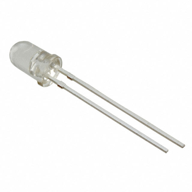
ICGOO电子元器件商城为您提供PT333-3C由Everlight设计生产,在icgoo商城现货销售,并且可以通过原厂、代理商等渠道进行代购。 PT333-3C价格参考。EverlightPT333-3C封装/规格:光学传感器 - 光电晶体管, Phototransistor 940nm Top View Radial, 5mm Dia (T 1 3/4)。您可以下载PT333-3C参考资料、Datasheet数据手册功能说明书,资料中有PT333-3C 详细功能的应用电路图电压和使用方法及教程。
| 参数 | 数值 |
| 产品目录 | |
| 描述 | PHOTOTRANSISTOR 5MM CLEAR RAD光电晶体管 IR Phototransistor |
| 产品分类 | |
| 品牌 | Everlight Electronics Co Ltd |
| 产品手册 | |
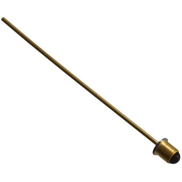
| 产品图片 |
|
| rohs | 符合RoHS无铅 / 符合限制有害物质指令(RoHS)规范要求 |
| 产品系列 | 光电晶体管,Everlight PT333-3C- |
| 数据手册 | |
| 产品型号 | PT333-3C |
| 上升时间 | 15 us |
| 下降时间 | 15 us |
| 产品 | Phototransistors |
| 产品种类 | 光电晶体管 |
| 其它名称 | 1080-1157 |
| 功率-最大值 | - |
| 商标 | Everlight |
| 安装类型 | 通孔 |
| 封装/外壳 | 径向,5mm 直径(T 1 3/4) |
| 封装/箱体 | T-1 |
| 工厂包装数量 | 500 |
| 最大功率耗散 | 75 mW |
| 最大工作温度 | + 85 C |
| 最大集电极电流 | 20 mA |
| 最小工作温度 | - 40 C |
| 朝向 | 顶视图 |
| 标准包装 | 500 |
| 波长 | 940nm |
| 电压-集射极击穿(最大值) | 30V |
| 电流-暗(Id)(最大值) | 100nA |
| 电流-集电极(Ic)(最大值) | 20mA |
| 视角 | - |
| 集电极—发射极最大电压VCEO | 30 V |
| 集电极—射极击穿电压 | 30 V |
| 集电极—射极饱和电压 | 0.4 V |


- 商务部:美国ITC正式对集成电路等产品启动337调查
- 曝三星4nm工艺存在良率问题 高通将骁龙8 Gen1或转产台积电
- 太阳诱电将投资9.5亿元在常州建新厂生产MLCC 预计2023年完工
- 英特尔发布欧洲新工厂建设计划 深化IDM 2.0 战略
- 台积电先进制程称霸业界 有大客户加持明年业绩稳了
- 达到5530亿美元!SIA预计今年全球半导体销售额将创下新高
- 英特尔拟将自动驾驶子公司Mobileye上市 估值或超500亿美元
- 三星加码芯片和SET,合并消费电子和移动部门,撤换高东真等 CEO
- 三星电子宣布重大人事变动 还合并消费电子和移动部门
- 海关总署:前11个月进口集成电路产品价值2.52万亿元 增长14.8%

PDF Datasheet 数据手册内容提取
5mm Phototransistor PT333-3C Features ․Fast response time ․High photo sensitivity ․Pb free ․The product itself will remain within RoHS compliant version. ․Copliance with EU REACH ․Compliance Halogen Free.(Br<900 ppm,Cl<900ppm,Br+Cl<1500ppm) Description ․PT333-3C is a high speed and high sensitive NPN silicon ․NPN epitaxial planar phototransistor molded in a standard 5 mm package. ․Due to its water clear epoxy the device is sensitive to infrared radiation. . Applications ․Infrared applied system ․Camera ․Printer ․Cockroach catcher 1 Copyright © 2010, Everlight All Rights Reserved. Release Date : 12.19.2016. Issue No: DPT-0000596_Rev.2 www.everlight.com
DATASHEET 5mm Phototransistor PT333-3C Device Selection Guide Chip Lens Color Materials Silicon Water clear Absolute Maximum Ratings (Ta=25℃) Parameter Symbol Rating Unit Collector-Emitter Voltage V 30 V CEO Emitter-Collector-Voltage V 5 V ECO Collector Current I 20 mA C Operating Temperature T -25~+85 °C opr Storage Temperature T -40~ +100 °C stg Lead Soldering Temperature*1 Tsol 260 °C Power Dissipation at (or below) P 75 mW c 25℃Free Air Temperature Notes: *1:Soldering time≦5 seconds. 2 Copyright © 2010, Everlight All Rights Reserved. Release Date : 12.19.2016. Issue No: DPT-0000596_Rev.2 www.everlight.com
DATASHEET 5mm Phototransistor PT333-3C Electro-Optical Characteristics (Ta=25℃) Parameter Symbol Min. Typ. Max. Unit Condition Collector – Emitter I =100μA BVCEO 30 ----- ----- V ECe=0mW/cm2 Breakdown Voltage Emitter-Collector I =100μA Breakdown Voltage BVECO 5 ----- ----- V EEe=0mW/cm2 Collector-Emitter I =2mA Saturation Voltage VCE(sat) ----- ----- 0.4 V ECe=1mW/cm2 Rise Time tr ----- 15 ----- VCE=5V μS I =1mA C Fall Time tf ----- 15 ----- RL=1000Ω Ee=0mW/cm2 Collector Dark Current I ----- ----- 100 nA CEO V =20V CE Ee=1mW/cm2 On State Collector Current IC(on) 0.7 4.0 ----- mA VCE=5V λp=940nm Rang Of Spectral Bandwidth λ0.5 400 ----- 1100 nm ---- Wavelength of Peak Sensitivity λP ----- 940 ----- nm ---- Rankings Parameter Symbol Min Max Unit Test Condition G 0.70 1.90 VcE=5V H 1.14 2.60 mA Ee=1mW/cm² Ic (ON) J 1.77 3.61 K 2.67 5.07 L 4.18 7.07 Note: *Measurement Uncertainty of Forward Voltage: ±0.1V *Measurement Uncertainty of Luminous Intensity: ±10% *Measurement Uncertainty of Dominant Wavelength ±1.0nm 3 Copyright © 2010, Everlight All Rights Reserved. Release Date : 12.19.2016. Issue No: DPT-0000596_Rev.2 www.everlight.com
DATASHEET 5mm Phototransistor PT333-3C Typical Electro-Optical Characteristics Curves Collector Power Dissipation vs. Ambient Temperature Spectral Sensitivity 100 1.0 Ta=25C 80 0.8 60 0.6 40 0.4 20 0.2 0 0 -25 0 25 50 75 85 100 700 800 900 1000 1100 1300 Relative Collector Current vs. Ambient Temperature Collector Current vs. Irradiance 100 160 140 2 C 120 10 100 80 1 60 40 0.1 20 0 0.01 0 10 20 30 40 50 60 70 0.5 1 1.5 3 2 4 Copyright © 2010, Everlight All Rights Reserved. Release Date : 12.19.2016. Issue No: DPT-0000596_Rev.2 www.everlight.com
DATASHEET 5mm Phototransistor PT333-3C Package Dimension Note: Tolerances unless dimensions ±0.25mm 5 Copyright © 2010, Everlight All Rights Reserved. Release Date : 12.19.2016. Issue No: DPT-0000596_Rev.2 www.everlight.com
DATASHEET 5mm Phototransistor PT333-3C Label Explanation ‧CPN: Customer’s Product Number ‧P/N: Product Number ‧QTY: Packing Quantity ‧CAT: Luminous Intensity Rank ‧HUE: Dom. Wavelength Rank ‧REF: Forward Voltage Rank ‧LOT No: Lot Number ‧X: Month ‧Reference: Identify Label Number Packing Specification ■ Anti-electrostatic bag ■ Inner Carton ■ Outside Carton ■ Packing Quantity 1. MIN 200 To 500 PCS/1 Bag, 5 Bags/1 Inner Carton 2. 10 Inner Cartons/1 Outside Carton 6 Copyright © 2010, Everlight All Rights Reserved. Release Date : 12.19.2016. Issue No: DPT-0000596_Rev.2 www.everlight.com
DATASHEET 5mm Phototransistor PT333-3C Notes 1. Lead Forming During lead formation, the leads should be bent at a point at least 3mm from the base of the epoxy bulb. Lead forming should be done before soldering. Avoid stressing the phototransistor package during leads forming. The stress to the base may damage the phototransistor’s characteristics or it may break the phototransistors. Cut the phototransistor lead frames at room temperature. Cutting the lead frames at high temperatures may cause failure of the phototransistors. When mounting the phototransistors onto a PCB, the PCB holes must be aligned exactly with the lead position of the phototransistor. If the phototransistors are mounted with stress at the leads, it causes deterioration of the epoxy resin and this will degrade the phototransistors. 2. Storage The phototransistors should be stored at 30°C or less and 70%RH or less after being shipped from Everlight and the storage life limits are 3 months. If the phototransistors are stored for 3 months or more, they can be stored for a year in a sealed container with a nitrogen atmosphere and moisture absorbent material. Please avoid rapid transitions in ambient temperature, especially, in high humidity environments where condensation can occur. 3. Soldering Careful attention should be paid during soldering. When soldering, leave more then 3mm from solder joint to epoxy bulb, and soldering beyond the base of the tie bar is recommended. Recommended soldering conditions: Hand Soldering DIP Soldering Temp. at tip of iron 300℃ Max. (30W Max.) Preheat temp. 100℃ Max. (60 sec Max.) Soldering time 3 sec Max. Bath temp. & time 260 Max., 5 sec Max Distance 3mm Min.(From solder Distance 3mm Min. (From solder joint to epoxy bulb) joint to epoxy bulb) Recommended soldering profile laminar wave Fluxing Prehead Avoiding applying any stress to the lead frame while the phototransistors are at high temperature particularly when soldering. 7 Copyright © 2010, Everlight All Rights Reserved. Release Date : 12.19.2016. Issue No: DPT-0000596_Rev.2 www.everlight.com
DATASHEET 5mm Phototransistor PT333-3C Dip and hand soldering should not be done more than one time After soldering the phototransistors, the epoxy bulb should be protected from mechanical shock or vibration until the phototransistors return to room temperature A rapid-rate process is not recommended for cooling the phototransistors down from the peak temperature. Although the recommended soldering conditions are specified in the above table, dip or hand soldering at the lowest possible temperature is desirable for the phototransistors. Wave soldering parameter must be set and maintain according to recommended temperature and dwell time in the solder wave. 4. Cleaning When necessary, cleaning should occur only with isopropyl alcohol at room temperature for a duration of no more than one minute. Dry at room temperature before use. Do not clean the phototransistors by the ultrasonic. When it is absolutely necessary, the influence of ultrasonic cleaning on the LEDs depends on factors such as ultrasonic power and the assembled condition. Ultrasonic cleaning shall be pre-qualified to ensure this will not cause damage to the phototransistor 5. Heat Management Heat management of phototransistors must be taken into consideration during the design stage of phototransistor application. The current should be de-rated appropriately by referring to the de-rating curve found in each product specification. The temperature surrounding the phototransistor in the application should be controlled. Please refer to the data sheet de-rating curve. 6. ESD (Electrostatic Discharge) Electrostatic discharge (ESD) or surge current (EOS) can damage phototransistors. An ESD wrist strap, ESD shoe strap or antistatic gloves must be worn whenever handling phototransistors. All devices, equipment and machinery must be properly grounded. Use ion blower to neutralize the static charge which might have built up on surface of the phototransistors plastic lens as a result of friction between phototransistors during storage and handing. DISCLAIMER 1. EVERLIGHT reserves the right(s) on the adjustment of product material mix for the specification. 2. The product meets EVERLIGHT published specification for a period of twelve (12) months from date of shipment. 3. The graphs shown in this datasheet are representing typical data only and do not show guaranteed values. 4. When using this product, please observe the absolute maximum ratings and the instructions for using outlined in these specification sheets. EVERLIGHT assumes no responsibility for any damage resulting from the use of the product which does not comply with the absolute maximum ratings and the instructions included in these specification sheets. 5. These specification sheets include materials protected under copyright of EVERLIGHT. Reproduction in any form is prohibited without obtaining EVERLIGHT’s prior consent. 8 Copyright © 2010, Everlight All Rights Reserved. Release Date : 12.19.2016. Issue No: DPT-0000596_Rev.2 www.everlight.com
DATASHEET 5mm Phototransistor PT333-3C 6. This product is not intended to be used for military, aircraft, automotive, medical, life sustaining or life saving applications or any other application which can result in human injury or death. Please contact authorized Everlight sales agent for special application request. 9 Copyright © 2010, Everlight All Rights Reserved. Release Date : 12.19.2016. Issue No: DPT-0000596_Rev.2 www.everlight.com