ICGOO在线商城 > 分立半导体产品 > 晶体管 - FET,MOSFET - 单 > PMZ250UN,315

 Datasheet下载
- 型号: PMZ250UN,315
- 制造商: NXP Semiconductors
- 库位|库存: xxxx|xxxx
- 要求:
| 数量阶梯 | 香港交货 | 国内含税 |
| +xxxx | $xxxx | ¥xxxx |
查看当月历史价格
查看今年历史价格
PMZ250UN,315产品简介:
ICGOO电子元器件商城为您提供PMZ250UN,315由NXP Semiconductors设计生产,在icgoo商城现货销售,并且可以通过原厂、代理商等渠道进行代购。 PMZ250UN,315价格参考。NXP SemiconductorsPMZ250UN,315封装/规格:晶体管 - FET,MOSFET - 单, 表面贴装 N 沟道 20V 2.28A(Tc) 2.5W(Tc) DFN1006-3。您可以下载PMZ250UN,315参考资料、Datasheet数据手册功能说明书,资料中有PMZ250UN,315 详细功能的应用电路图电压和使用方法及教程。
| 参数 | 数值 |
| 产品目录 | |
| 描述 | MOSFET N-CH 20V 2.28A SOT883MOSFET TAPE7 MOSFET |
| 产品分类 | FET - 单分离式半导体 |
| FET功能 | 逻辑电平门 |
| FET类型 | MOSFET N 通道,金属氧化物 |
| Id-连续漏极电流 | 2.28 A |
| 品牌 | NXP Semiconductors |
| 产品手册 | |
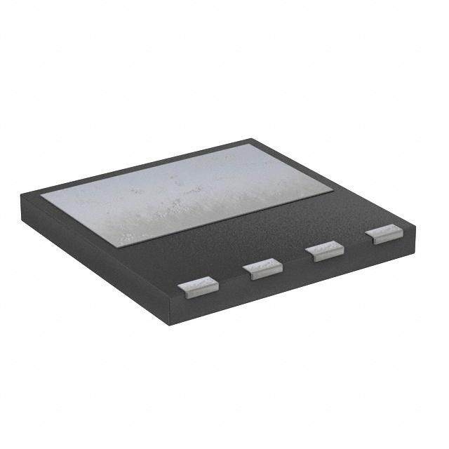
| 产品图片 |
|
| rohs | 符合RoHS无铅 / 符合限制有害物质指令(RoHS)规范要求 |
| 产品系列 | 晶体管,MOSFET,NXP Semiconductors PMZ250UN,315TrenchMOS™ |
| 数据手册 | |
| 产品型号 | PMZ250UN,315 |
| PCN封装 | |
| Pd-PowerDissipation | 2.5 W |
| Pd-功率耗散 | 2.5 W |
| RdsOn-漏源导通电阻 | 300 mOhms |
| Vds-漏源极击穿电压 | 20 V |
| Vgs-Gate-SourceBreakdownVoltage | +/- 8 V |
| Vgs-栅源极击穿电压 | 8 V |
| 上升时间 | 10 ns |
| 下降时间 | 5 ns |
| 不同Id时的Vgs(th)(最大值) | 950mV @ 250µA |
| 不同Vds时的输入电容(Ciss) | 45pF @ 20V |
| 不同Vgs时的栅极电荷(Qg) | 0.89nC @ 4.5V |
| 不同 Id、Vgs时的 RdsOn(最大值) | 300 毫欧 @ 200mA,4.5V |
| 产品种类 | MOSFET |
| 供应商器件封装 | SOT-883 |
| 其它名称 | 568-6775-2 |
| 典型关闭延迟时间 | 18.5 ns |
| 功率-最大值 | 2.5W |
| 包装 | 带卷 (TR) |
| 商标 | NXP Semiconductors |
| 安装类型 | 表面贴装 |
| 安装风格 | SMD/SMT |
| 导通电阻 | 300 mOhms |
| 封装 | Reel |
| 封装/外壳 | SC-101,SOT-883 |
| 封装/箱体 | SC-101-3 |
| 工厂包装数量 | 10000 |
| 晶体管极性 | N-Channel |
| 最大工作温度 | + 150 C |
| 最小工作温度 | - 55 C |
| 标准包装 | 10,000 |
| 汲极/源极击穿电压 | 20 V |
| 漏极连续电流 | 2.28 A |
| 漏源极电压(Vdss) | 20V |
| 特色产品 | http://www.digikey.cn/product-highlights/cn/zh/low-rdson-mosfets-in-ultra-small-packages/3946 |
| 电流-连续漏极(Id)(25°C时) | 2.28A (Tc) |
| 通道模式 | Enhancement |
| 配置 | Single |
| 零件号别名 | PMZ250UN T/R |


- 商务部:美国ITC正式对集成电路等产品启动337调查
- 曝三星4nm工艺存在良率问题 高通将骁龙8 Gen1或转产台积电
- 太阳诱电将投资9.5亿元在常州建新厂生产MLCC 预计2023年完工
- 英特尔发布欧洲新工厂建设计划 深化IDM 2.0 战略
- 台积电先进制程称霸业界 有大客户加持明年业绩稳了
- 达到5530亿美元!SIA预计今年全球半导体销售额将创下新高
- 英特尔拟将自动驾驶子公司Mobileye上市 估值或超500亿美元
- 三星加码芯片和SET,合并消费电子和移动部门,撤换高东真等 CEO
- 三星电子宣布重大人事变动 还合并消费电子和移动部门
- 海关总署:前11个月进口集成电路产品价值2.52万亿元 增长14.8%


PDF Datasheet 数据手册内容提取
Important notice Dear Customer, On 7 February 2017 the former NXP Standard Product business became a new company with the tradename Nexperia. Nexperia is an industry leading supplier of Discrete, Logic and PowerMOS semiconductors with its focus on the automotive, industrial, computing, consumer and wearable application markets In data sheets and application notes which still contain NXP or Philips Semiconductors references, use the references to Nexperia, as shown below. Instead of http://www.nxp.com, http://www.philips.com/ or http://www.semiconductors.philips.com/, use http://www.nexperia.com Instead of sales.addresses@www.nxp.com or sales.addresses@www.semiconductors.philips.com, use salesaddresses@nexperia.com (email) Replace the copyright notice at the bottom of each page or elsewhere in the document, depending on the version, as shown below: - © NXP N.V. (year). All rights reserved or © Koninklijke Philips Electronics N.V. (year). All rights reserved Should be replaced with: - © Nexperia B.V. (year). All rights reserved. If you have any questions related to the data sheet, please contact our nearest sales office via e-mail or telephone (details via salesaddresses@nexperia.com). Thank you for your cooperation and understanding, Kind regards, Team Nexperia
PMZ250UN N-channel TrenchMOS extremely low level FET Rev. 01 — 21 February 2008 Product data sheet BOTTOM VIEW 1. Product profile 1.1 General description N-channel enhancement mode Field-Effect Transistor (FET) in a plastic package using TrenchMOS technology. 1.2 Features n Profile 55 % lower than SOT23 n Footprint 90 % smaller than SOT23 n Lower on-state resistance n Low threshold voltage n Leadless package n Fast switching 1.3 Applications n Driver circuits n Load switching in portable appliances n DC-to-DC converters 1.4 Quick reference data n V £ 20V n I £ 2.28A DS D n R £ 300mW n P £ 2.50W DSon tot 2. Pinning information Table 1. Pinning Pin Description Simplified outline Symbol 1 gate (G) 2 source (S) 1 D 3 3 drain (D) 2 G Transparent top view SOT883 (SC-101) mbb076 S
PMZ250UN NXP Semiconductors N-channel TrenchMOS extremely low level FET 3. Ordering information Table 2. Ordering information Type number Package Name Description Version PMZ250UN SC-101 leadless ultra small plastic package; 3 solder lands; SOT883 body1.0· 0.6· 0.5mm 4. Limiting values CAUTION This device is sensitive to ElectroStatic Discharge (ESD). Observe precautions for handling electrostatic sensitive devices. Such precautions are described in theANSI/ESD S20.20,IEC/ST61340-5,JESD625-A or equivalent standards. Table 3. Limiting values In accordance with the Absolute Maximum Rating System (IEC 60134). Symbol Parameter Conditions Min Max Unit V drain-source voltage 25(cid:176) C£ T £ 150(cid:176) C - 20 V DS j V drain-gate voltage (DC) 25(cid:176) C£ T £ 150(cid:176) C; R =20kW - 20 V DGR j GS V gate-source voltage - – 8 V GS I drain current T =25(cid:176) C; V =4.5V; seeFigure2 and3 - 2.28 A D sp GS T =100(cid:176) C; V =4.5V; seeFigure2 - 1.44 A sp GS I peak drain current T =25(cid:176) C; pulsed; t £ 10m s; seeFigure3 - 4.56 A DM sp p P total power dissipation T =25(cid:176) C; seeFigure1 - 2.50 W tot sp T storage temperature - - 55 +150 (cid:176) C stg T junction temperature - - 55 +150 (cid:176) C j Source-drain diode I source current T =25(cid:176) C - 2.28 A S sp I peak source current T =25(cid:176) C; pulsed; t £ 10m s - 4.56 A SM sp p Electrostatic discharge V electrostatic discharge voltage all pins - esd human body model; C = 100pF; R = 1.5 kW - 60 V machine model; C = 200 pF - 30 V PMZ250UN_1 © NXP B.V. 2008. All rights reserved. Product data sheet Rev. 01 — 21 February 2008 2 of 13
PMZ250UN NXP Semiconductors N-channel TrenchMOS extremely low level FET 003aac031 003aac033 120 120 Pder Ider (%) ( %) 80 80 40 40 0 0 0 50 100 150 200 0 50 100 150 200 Tsp ((cid:176)C) Tsp ((cid:176)C) P I P = ------------t-o---t--------· 100% I = ----------D----------· 100% der Ptot(25(cid:176) C) der ID(25(cid:176) C) Fig 1. Normalized total power dissipation as a Fig 2. Normalized continuous drain current as a function of solder point temperature function of solder point temperature 102 003aac202 ID (A) Limit RDSon = VDS / ID 10 tp = 10 m s 100 m s 1 1 ms DC 10 ms 10- 1 100 ms 10- 2 10- 1 1 10 102 VDS (V) T =25(cid:176) C; I is single pulse sp DM Fig 3. Safe operating area; continuous and peak drain currents as a function of drain-source voltage PMZ250UN_1 © NXP B.V. 2008. All rights reserved. Product data sheet Rev. 01 — 21 February 2008 3 of 13
PMZ250UN NXP Semiconductors N-channel TrenchMOS extremely low level FET 5. Thermal characteristics Table 4. Thermal characteristics Symbol Parameter Conditions Min Typ Max Unit R thermal resistance from junction to solder point seeFigure4 - - 50 K/W th(j-sp) R thermal resistance from junction to ambient minimumfootprint [1] - 670 - K/W th(j-a) [1] Mounted on a printed-circuit board; verticalinstillair. 102 003aab831 Z th(j-sp) (K/W) d = 0.5 0.2 10 0.1 0.05 P d = tp T 0.02 single pulse tp t T 1 10-4 10-3 10-2 10-1 1 10 t (s) p Fig 4. Transient thermal impedance from junction to solder point as a function of pulse duration PMZ250UN_1 © NXP B.V. 2008. All rights reserved. Product data sheet Rev. 01 — 21 February 2008 4 of 13
PMZ250UN NXP Semiconductors N-channel TrenchMOS extremely low level FET 6. Characteristics Table 5. Characteristics T=25(cid:176) C unless otherwise specified. j Symbol Parameter Conditions Min Typ Max Unit Static characteristics V drain-source breakdown I =10m A; V =0V (BR)DSS D GS voltage T =25(cid:176) C 20 - - V j T =- 55(cid:176) C 18 - - V j V gate-source threshold voltage I =0.25mA;V =V ;seeFigure9and10 GS(th) D DS GS T =25(cid:176) C 0.45 0.7 0.95 V j T =150(cid:176) C 0.25 - - V j T =- 55(cid:176) C - - 1.15 V j I drain leakage current V =20V; V =0V DSS DS GS T =25(cid:176) C - - 1 m A j T =150(cid:176) C - - 100 m A j I gate leakage current V =– 8V; V =0V - 10 100 nA GSS GS DS R drain-source on-state V =4.5V; I =0.2A; seeFigure6 and8 DSon GS D resistance T =25(cid:176) C - 250 300 mW j T =150(cid:176) C - 400 480 mW j V =2.5V; I =0.1A; seeFigure6 and8 - 320 400 mW GS D V =1.8V; I =0.075A; seeFigure6 and8 - 420 600 mW GS D Dynamic characteristics Q total gate charge I =1A; V =10V; V =4.5V; see - 0.89 - nC G(tot) D DS GS Figure11 and12 Q gate-source charge - 0.13 - nC GS Q gate-drain charge - 0.18 - nC GD C input capacitance V =0V; V =20V; f=1MHz; see - 45 - pF iss GS DS Figure14 C output capacitance - 11 - pF oss C reverse transfer capacitance - 7 - pF rss t turn-on delay time V =10V; R =10W ; V =4.5V; R =6W - 4.5 - ns d(on) DS L GS G t rise time - 10 - ns r t turn-off delay time - 18.5 - ns d(off) t fall time - 5 - ns f Source-drain diode V source-drain voltage I =0.3A; V =0V; seeFigure13 - 0.80 1.2 V SD S GS PMZ250UN_1 © NXP B.V. 2008. All rights reserved. Product data sheet Rev. 01 — 21 February 2008 5 of 13
PMZ250UN NXP Semiconductors N-channel TrenchMOS extremely low level FET 03an02 03an03 2.5 1 ID 4.5 3 2.5 RDSon VGS (V) = 1.8 2 (A) (W ) 2 0.8 2 1.5 0.6 2.5 1.8 1 0.4 3 4.5 0.5 VGS (V) = 1.5 0.2 0 0 0 0.5 1 1.5 2 0 0.5 1 1.5 2 2.5 VDS (V) ID (A) T =25(cid:176) C T =25(cid:176) C j j Fig 5. Output characteristics: drain current as a Fig 6. Drain-source on-state resistance as a function function of drain-source voltage; typical values of drain current; typical values 03an04 003aac024 2.5 2.0 ID a (A) 2 25 (cid:176)C Tj = 150 (cid:176)C 1.5 1.5 1.0 1 0.5 0.5 0 0 0 1 2 3 4 - 60 0 60 120 180 VGS (V) Tj ((cid:176)C) Tj=25(cid:176) C and 150(cid:176) C; VDS>ID· RDSon R a = ------------D----S--o---n--------- RDSon(25(cid:176) C) Fig 7. Transfer characteristics: drain current as a Fig 8. Normalized drain-source on-state resistance function of gate-source voltage; typical values factor as a function of junction temperature PMZ250UN_1 © NXP B.V. 2008. All rights reserved. Product data sheet Rev. 01 — 21 February 2008 6 of 13
PMZ250UN NXP Semiconductors N-channel TrenchMOS extremely low level FET 1.2 03aj65 10- 3 03am43 VGS(th) (V) ID (A) 0.9 max 10- 4 min typ max typ 0.6 min 10- 5 0.3 0 10- 6 - 60 0 60 120 180 0 0.4 0.8 1.2 Tj ((cid:176)C) VGS (V) I =0.25mA; V =V T =25(cid:176) C; V =5V D DS GS j DS Fig 9. Gate-source threshold voltage as a function of Fig 10. Sub-threshold drain current as a function of junction temperature gate-source voltage 03an07 5 V(VG)S ITDj == 215 A (cid:176)C VDS = 10 V 4 VDS ID 3 VGS(pl) 2 VGS(th) 1 VGS QGS1 QGS2 QGS QGD 0 QG(tot) 0 0.2 0.4 0.6 0.8 1 QG (nC) 003aaa508 I =1A; V =10V D DS Fig 11. Gate-source voltage as a function of gate Fig 12. Gate charge waveform definitions charge; typical values PMZ250UN_1 © NXP B.V. 2008. All rights reserved. Product data sheet Rev. 01 — 21 February 2008 7 of 13
PMZ250UN NXP Semiconductors N-channel TrenchMOS extremely low level FET 1 03an97 102 03an06 IS VGS = 0 V (A) 0.8 C Ciss (pF) 0.6 10 Coss 0.4 Crss 0.2 150 (cid:176)C Tj = 25 (cid:176)C 0 1 0 0.2 0.4 0.6 0.8 1 10- 1 1 10 102 VSD (V) VDS (V) T =25(cid:176) C and 150(cid:176) C; V =0V V =0V; f=1MHz j GS GS Fig 13. Source current as a function of source-drain Fig 14. Input,outputandreversetransfercapacitances voltage; typical values as a function of drain-source voltage; typical values PMZ250UN_1 © NXP B.V. 2008. All rights reserved. Product data sheet Rev. 01 — 21 February 2008 8 of 13
PMZ250UN NXP Semiconductors N-channel TrenchMOS extremely low level FET 7. Package outline Leadless ultra small plastic package; 3 solder lands; body 1.0 x 0.6 x 0.5 mm SOT883 L L1 2 b 3 e b1 1 e1 A A1 E D 0 0.5 1 mm scale DIMENSIONS (mm are the original dimensions) UNIT A(1) mAa1x. b b1 D E e e1 L L1 0.50 0.20 0.55 0.62 1.02 0.30 0.30 mm 0.03 0.35 0.65 0.46 0.12 0.47 0.55 0.95 0.22 0.22 Note 1. Including plating thickness OUTLINE REFERENCES EUROPEAN ISSUE DATE VERSION IEC JEDEC JEITA PROJECTION 03-02-05 SOT883 SC-101 03-04-03 Fig 15. Package outline SOT833 (SC-101) PMZ250UN_1 © NXP B.V. 2008. All rights reserved. Product data sheet Rev. 01 — 21 February 2008 9 of 13
PMZ250UN NXP Semiconductors N-channel TrenchMOS extremely low level FET 8. Soldering 1.30 R = 0.05 (12· ) 0.30 R = 0.05 (12· ) 0.35 solder lands (2· ) solder resist 0.90 0.20 0.60 0.70 0.80 occupied area 0.25 (2· ) solder paste 0.30 (2· ) 0.30 0.40 (2· ) 0.40 0.50 (2· ) 0.50 mbl873 Dimensions in mm Fig 16. Reflow soldering footprint for SOT883 PMZ250UN_1 © NXP B.V. 2008. All rights reserved. Product data sheet Rev. 01 — 21 February 2008 10 of 13
PMZ250UN NXP Semiconductors N-channel TrenchMOS extremely low level FET 9. Revision history Table 6. Revision history Document ID Release date Data sheet status Change notice Supersedes PMZ250UN_1 20080221 Product data sheet - - PMZ250UN_1 © NXP B.V. 2008. All rights reserved. Product data sheet Rev. 01 — 21 February 2008 11 of 13
PMZ250UN NXP Semiconductors N-channel TrenchMOS extremely low level FET 10. Legal information 10.1 Data sheet status Document status[1][2] Product status[3] Definition Objective [short] data sheet Development This document contains data from the objective specification for product development. Preliminary [short] data sheet Qualification This document contains data from the preliminary specification. Product [short] data sheet Production This document contains the product specification. [1] Please consult the most recently issued document before initiating or completing a design. [2] The term ‘short data sheet’ is explained in section “Definitions”. [3] Theproductstatusofdevice(s)describedinthisdocumentmayhavechangedsincethisdocumentwaspublishedandmaydifferincaseofmultipledevices.Thelatestproductstatus information is available on the Internet at URLhttp://www.nxp.com. 10.2 Definitions damage. NXP Semiconductors accepts no liability for inclusion and/or use of NXP Semiconductors products in such equipment or applications and therefore such inclusion and/or use is at the customer’s own risk. Draft —The document is a draft version only. The content is still under internal review and subject to formal approval, which may result in Applications —Applications that are described herein for any of these modifications or additions. NXP Semiconductors does not give any products are for illustrative purposes only. NXP Semiconductors makes no representations or warranties as to the accuracy or completeness of representation or warranty that such applications will be suitable for the informationincludedhereinandshallhavenoliabilityfortheconsequencesof specified use without further testing or modification. use of such information. Quick reference data —The Quick reference data is an extract of the Short data sheet —A short data sheet is an extract from a full data sheet product data given in the Limiting values and Characteristics sections of this withthesameproducttypenumber(s)andtitle.Ashortdatasheetisintended document, and as such is not complete, exhaustive or legally binding. forquickreferenceonlyandshouldnotbereliedupontocontaindetailedand Limiting values —Stress above one or more limiting values (as defined in full information. For detailed and full information see the relevant full data theAbsoluteMaximumRatingsSystemofIEC60134)maycausepermanent sheet, which is available on request via the local NXP Semiconductors sales damagetothedevice.Limitingvaluesarestressratingsonlyandoperationof office. In case of any inconsistency or conflict with the short data sheet, the the device at these or any other conditions above those given in the full data sheet shall prevail. Characteristics sections of this document is not implied. Exposure to limiting values for extended periods may affect device reliability. 10.3 Disclaimers Terms and conditions of sale —NXP Semiconductors products are sold subjecttothegeneraltermsandconditionsofcommercialsale,aspublished athttp://www.nxp.com/profile/terms, including those pertaining to warranty, General —Information in this document is believed to be accurate and intellectual property rights infringement and limitation of liability, unless reliable.However,NXPSemiconductorsdoesnotgiveanyrepresentationsor explicitly otherwise agreed to in writing by NXP Semiconductors. In case of warranties,expressedorimplied,astotheaccuracyorcompletenessofsuch any inconsistency or conflict between information in this document and such information and shall have no liability for the consequences of use of such terms and conditions, the latter will prevail. information. No offer to sell or license —Nothing in this document may be interpreted Right to make changes —NXPSemiconductorsreservestherighttomake or construed as an offer to sell products that is open for acceptance or the changes to information published in this document, including without grant,conveyanceorimplicationofanylicenseunderanycopyrights,patents limitation specifications and product descriptions, at any time and without or other industrial or intellectual property rights. notice.Thisdocumentsupersedesandreplacesallinformationsuppliedprior to the publication hereof. Suitability for use —NXP Semiconductors products are not designed, 10.4 Trademarks authorized or warranted to be suitable for use in medical, military, aircraft, space or life support equipment, nor in applications where failure or Notice:Allreferencedbrands,productnames,servicenamesandtrademarks malfunction of an NXP Semiconductors product can reasonably be expected are the property of their respective owners. to result in personal injury, death or severe property or environmental TrenchMOS —is a trademark of NXP B.V. 11. Contact information For additional information, please visit:http://www.nxp.com For sales office addresses, send an email to:salesaddresses@nxp.com PMZ250UN_1 © NXP B.V. 2008. All rights reserved. Product data sheet Rev. 01 — 21 February 2008 12 of 13
PMZ250UN NXP Semiconductors N-channel TrenchMOS extremely low level FET 12. Contents 1 Product profile. . . . . . . . . . . . . . . . . . . . . . . . . . 1 1.1 General description. . . . . . . . . . . . . . . . . . . . . . 1 1.2 Features . . . . . . . . . . . . . . . . . . . . . . . . . . . . . . 1 1.3 Applications . . . . . . . . . . . . . . . . . . . . . . . . . . . 1 1.4 Quick reference data. . . . . . . . . . . . . . . . . . . . . 1 2 Pinning information. . . . . . . . . . . . . . . . . . . . . . 1 3 Ordering information. . . . . . . . . . . . . . . . . . . . . 2 4 Limiting values. . . . . . . . . . . . . . . . . . . . . . . . . . 2 5 Thermal characteristics. . . . . . . . . . . . . . . . . . . 4 6 Characteristics. . . . . . . . . . . . . . . . . . . . . . . . . . 5 7 Package outline . . . . . . . . . . . . . . . . . . . . . . . . . 9 8 Soldering . . . . . . . . . . . . . . . . . . . . . . . . . . . . . 10 9 Revision history. . . . . . . . . . . . . . . . . . . . . . . . 11 10 Legal information. . . . . . . . . . . . . . . . . . . . . . . 12 10.1 Data sheet status . . . . . . . . . . . . . . . . . . . . . . 12 10.2 Definitions. . . . . . . . . . . . . . . . . . . . . . . . . . . . 12 10.3 Disclaimers. . . . . . . . . . . . . . . . . . . . . . . . . . . 12 10.4 Trademarks. . . . . . . . . . . . . . . . . . . . . . . . . . . 12 11 Contact information. . . . . . . . . . . . . . . . . . . . . 12 12 Contents. . . . . . . . . . . . . . . . . . . . . . . . . . . . . . 13 Pleasebeawarethatimportantnoticesconcerningthisdocumentandtheproduct(s) described herein, have been included in section ‘Legal information’. © NXP B.V. 2008. All rights reserved. For more information, please visit: http://www.nxp.com For sales office addresses, please send an email to: salesaddresses@nxp.com Date of release: 21 February 2008 Document identifier: PMZ250UN_1