ICGOO在线商城 > PM113-625.0M

 Datasheet下载
- 型号: PM113-625.0M
- 制造商: Connor-Winfield
- 库位|库存: xxxx|xxxx
- 要求:
| 数量阶梯 | 香港交货 | 国内含税 |
| +xxxx | $xxxx | ¥xxxx |
查看当月历史价格
查看今年历史价格
PM113-625.0M产品简介:
ICGOO电子元器件商城为您提供PM113-625.0M由Connor-Winfield设计生产,在icgoo商城现货销售,并且可以通过原厂、代理商等渠道进行代购。 提供PM113-625.0M价格参考以及Connor-WinfieldPM113-625.0M封装/规格参数等产品信息。 你可以下载PM113-625.0M参考资料、Datasheet数据手册功能说明书, 资料中有PM113-625.0M详细功能的应用电路图电压和使用方法及教程。
| 参数 | 数值 |
| 产品目录 | 晶体和振荡器 |
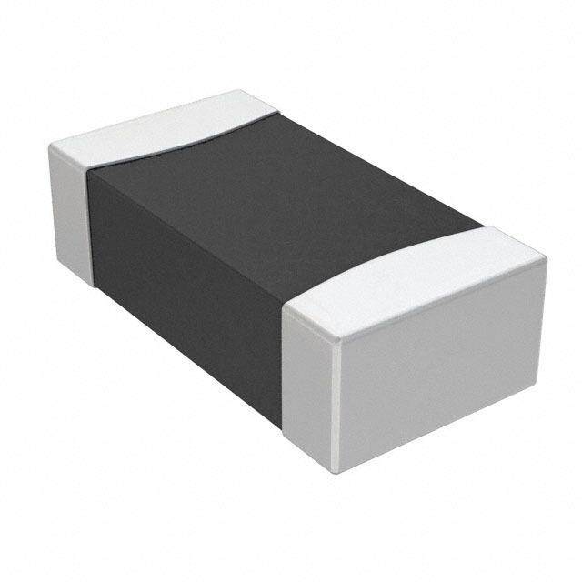
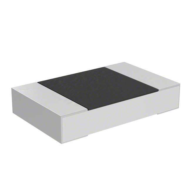
| 描述 | OSC XO 625.000MHZ LVPECL SMD |
| 产品分类 | |
| 品牌 | Connor-Winfield |
| 数据手册 | |
| 产品图片 |
|
| 产品型号 | PM113-625.0M |
| rohs | 无铅 / 符合限制有害物质指令(RoHS)规范要求 |
| 产品系列 | PM |
| 产品目录绘图 |
|
| 产品目录页面 | |
| 其它名称 | CW673 |
| 功能 | 三态(输出启用) |
| 包装 | 剪带 |
| 大小/尺寸 | 0.276" 长 x 0.197" 宽(7.00mm x 5.00mm) |
| 安装类型 | 表面贴装 |
| 封装/外壳 | 6-SMD,无引线(DFN,LCC) |
| 工作温度 | 0°C ~ 70°C |
| 标准包装 | 25 |
| 特色产品 | http://www.digikey.com/cn/zh/ph/ConnorWinfield/LM113_PM113.html |
| 电压-电源 | 3.3V |
| 电流-电源(最大值) | 95mA |
| 电流-电源(禁用)(最大值) | - |
| 等级 | - |
| 类型 | XO(标准) |
| 输出 | LVPECL |
| 频率 | 625MHz |
| 频率稳定度 | ±25ppm |
| 高度 | 0.069"(1.75mm) |


%20Series%20Top.jpg)


- 商务部:美国ITC正式对集成电路等产品启动337调查
- 曝三星4nm工艺存在良率问题 高通将骁龙8 Gen1或转产台积电
- 太阳诱电将投资9.5亿元在常州建新厂生产MLCC 预计2023年完工
- 英特尔发布欧洲新工厂建设计划 深化IDM 2.0 战略
- 台积电先进制程称霸业界 有大客户加持明年业绩稳了
- 达到5530亿美元!SIA预计今年全球半导体销售额将创下新高
- 英特尔拟将自动驾驶子公司Mobileye上市 估值或超500亿美元
- 三星加码芯片和SET,合并消费电子和移动部门,撤换高东真等 CEO
- 三星电子宣布重大人事变动 还合并消费电子和移动部门
- 海关总署:前11个月进口集成电路产品价值2.52万亿元 增长14.8%


PDF Datasheet 数据手册内容提取
5x7mm Surface Mount LVPECL Clock Oscillator Description: CW Features: The Connor-Winfield PMxxx - Series are 155.52PMM11H02z430 M5xo7dmeml P SMuxrfxaxc e- SMeoruienst Package 2111 Comprehensive Drive 5x7mm Surface Mount, LVPECL, Fixed 2.5 or 3.3 Vdc Operation 2111 Comprehensive Drive Frequency Crystal Controlled Oscillator LVPECL Differential Outputs Aurora, Illinois 60505 (XO). The PMxxx - Series are designed for Frequency Stabilities Available: Aurora, Illinois 60505 applications requiring tight frequency stability, wide +/-20 ppm, +/-25 ppm, +/-50 ppm or +/-100 ppm Phone: 630-851-4722 temperature range, and low jitter. Operating at Temperature Ranges Available: Phone: 630-851-4722 2.5 or 3.3 Vdc supply voltage, the PMxxx - Series 0 to 70°C, -40 to 85°C, 0 to 85°C or -20 to 70°C Fax: 630-851-5040 Low Jitter <1ps RMS Fax: 630-851-5040 provides LVPECL Differential Outputs with an Tri-State Enable/Disable on Pad 1 wwwwww..ccoonnwwiinn..ccoomm emnualtbipleli c/ adtiisoanb tloe pfurondctuiocne. aT hheig dhe fsreigqnu eunticlizye osu PtpLuLt TRaopHeS a Cndo mRpeleial nPta /c Lkeaagdin Fgree US Headquarters: from a low frequency fundamental crystal. 630-851-4722 Absolute Maximum Ratings European Headquarters: Parameter Minimum Nominal Maximum Units Notes +353-61-472221 Storage Temperature -55 - 125 °C Supply Voltage (Vcc) -0.5 - 4.6 Vdc Input Voltage -0.5 - Vcc + 0.5 Vdc Operating Specifications Parameter Minimum Nominal Maximum Units Notes Output Frequency (Fo) 98 - 673 MHz 1 Total Frequency Tolerance (See Ordering Information or Model Matrix for full part number) Model PMx4x -20 - 20 ppm 2 Model PMx1x -25 - 25 ppm 2 Model PMx2x -50 - 50 ppm 2 Model PMx3x -100 - 100 ppm 2 Operating Temperature Range (See Ordering Information or Model Matrix for full part number) Model PM1xx 0 - 70 °C Model PM2xx -40 - 85 °C Model PM3xx 0 - 85 °C Model PM4xx -20 - 70 °C Supply Voltage (Vcc) (See Ordering Information or Model Matrix for full part number) Model PMxx2 2.375 2.5 2.625 Vdc Model PMxx3 3.135 3.3 3.465 Vdc Supply Current (Icc) - 85 95 mA Jitter: Period Jitter - 3.0 5.0 ps RMS Integrated Phase Jitter - 0.6 1.0 ps RMS SSB Phase Noise (Fo = 155.52 MHz) @ 10 Hz offset - -40 - dBc/Hz @ 100 Hz offset - -75 - dBc/Hz @ 1 KHz offset - -95 - dBc/Hz @ 10 KHz offset - -110 - dBc/Hz @ 100 KHz offset - -115 - dBc/Hz Sub-Harmonics - -60 -50 dBc Start-Up Time - - 2 ms Enable / Disable Input Characteristics Parameter Minimum Nominal Maximum Units Notes Enable Input Voltage - (High) -(Vih) 70%Vcc - - Vdc 3 Disable Input Voltage - (Low) - (Vil) - - 30%Vcc Vdc 3 LVPECL Output Characteristics Parameter Minimum Nominal Maximum Units Notes Load - - 50 - Ohm 4 Voltage (High) (Voh) Vcc-1.025 - - V (Low) (Vol) - - Vcc-1.620 V Duty Cycle at 50% Level 45 50 55 % 5 Rise / Fall Time: 20% to 80% - 0.3 0.6 ns Package Characteristics Package Hermetically sealed ceramic package and metal cover Environmental Characteristics Vibration: Vibration per Mil Std 883E Method 2007.3 Test Condition A. Shock: Mechanical Shock per Mil Std 883E Method 2002.4 Test Condition B. Soldering Process; RoHS compliant lead free. See soldering profile on page 2. Bulletin Ec262 Notes: Page 1 of 2 1. All output frequencies may not be available, please contact the factory with your output frequency requirements. Revision 01 2. Includes calibration @ 25°C, frequency stability vs. change in temperature, supply voltage and load variations, shock and vibration and 20 years aging. 3. When the oscillator is disabled the outputs are at high impedance. Outputs are enabled with no connection on E/D pad 1. Date 10 Mar 2011 4. Outputs must be terminated into 50 ohms to Vcc – 2V or Thevenin equivalent. 5. Duty cycle measured at 50% of output voltage swing. Specifications subject to change without notice. All dimensions in inches. © Copyright 2010 The Connor-Winfield Corporation
2111 Comprehensive Drive Aurora, Illinois 60505 Phone: 630-851-4722 Fax: 630-851-5040 www.conwin.com Ordering Information Package Outline PM 1 2 3 - 155.52M 0.275 0.055 Output Frequency (7.0mm) (1.4mm) Type Temperature Frequency Supply Voltage Range Tolerance Frequency Format CW 1040 LVPECL 2 = 2.5 Vdc, -xxx.xM Min Clock Series 1 = 0 to 70°C 4 = ±20 ppm 3 = 3.3 Vdc, -xxx.xxxxxxM Max 0.197 PM123 5x7 mm 2 = -40 to 85°C 1 = ±25 ppm *Amount of numbers (5.0mm) 155.52MHZ 3 = 0 to 85°C 2 = ±50 ppm after the decimal 4 = -20 to 70°C 3 = ±100 ppm point. M = MHz 0.102 Example Part Number: .069 (2.6mm) PM123-155.52M = LVPECL Output, 0 to 70°C, +/-50ppm, 3.3Vdc, E/D Pad 1, Output Frequency 155.52 MHz (1.75mm) DimensionalTolerance +/-0.008(+/-0.2mm) Note: Not all temperature and frequency tolerance combinations are available. See Model Matrix below for available models Model Matrix Suggested Pad Layout Frequency Frequency Frequency Frequency Supply Temperature Tolerance Tolerance Tolerance Tolerance Voltage Range ±20 ppm ±25 ppm ±50 ppm ±100 ppm 0.200 (5.08mm) PM142 PM112 PM122 PM132 2.5 Vdc 0 to 70°C 0.100 (2.54mm) PM442 PM412 PM422 PM432 2.5 Vdc -20 to 70°C 6 5 4 0.079 PM342 PM312 PM322 PM332 2.5 Vdc 0 to 85°C (2.0mm) X X PM222 PM232 2.5 Vdc -40 to 85°C 0.165 Top (4.2mm) View Bypass PM143 PM113 PM123 PM133 3.3 Vdc 0 to 70°C Capacitor PM443 PM413 PM423 PM433 3.3 Vdc -20 to 70°C 1 2 3 Gro0u.n0d1uF PM343 PM313 PM323 PM333 3.3 Vdc 0 to 85°C 0.070 (1.78mm) X X PM223 PM233 3.3 Vdc -40 to 85°C X = Models not available Enable / Disable Function Pad Connections 1: Enable / Disable Pad 1 Input: Output State: 2 N/C Low: Disabled (High Impedance) 3: Ground High or Open: Enabled 4: Output Q 5: Complementary Output Q 6: Supply Voltage (Vcc) Test Circuit Output Waveform R3 DutyCycle Q 654 R4 80% 1 23 R1 50% E/D 20% N/C R2 Q Vcc R1/R3 R2/R4 tr tf Vcc=Vcc2 2.5V 250Ohms 62.5Ohms 3.3V 130Ohms 82Ohms Tape and Reel Dimensions Solder Profile Temperature 260°C 260°C 220°C 180°C 150°C 120°C 0 Time 120S 10S Max. 60S Max. 360Sec.Max. Bulletin EC262 Page 2 of 2 Dimensional Tolerance: ±.02” (.508mm) ±.005” (.127mm) Revision 01 Date 10 Mar 2011 Specifications subject to change without notice. All dimensions in inches. © Copyright 2010 The Connor-Winfield Corporation