ICGOO在线商城 > PL123-05NSC-R

 Datasheet下载
- 型号: PL123-05NSC-R
- 制造商: Micrel
- 库位|库存: xxxx|xxxx
- 要求:
| 数量阶梯 | 香港交货 | 国内含税 |
| +xxxx | $xxxx | ¥xxxx |
查看当月历史价格
查看今年历史价格
PL123-05NSC-R产品简介:
ICGOO电子元器件商城为您提供PL123-05NSC-R由Micrel设计生产,在icgoo商城现货销售,并且可以通过原厂、代理商等渠道进行代购。 提供PL123-05NSC-R价格参考以及MicrelPL123-05NSC-R封装/规格参数等产品信息。 你可以下载PL123-05NSC-R参考资料、Datasheet数据手册功能说明书, 资料中有PL123-05NSC-R详细功能的应用电路图电压和使用方法及教程。
| 参数 | 数值 |
| 产品目录 | 集成电路 (IC)半导体 |
| 描述 | IC CLK BUFFER 1:5 134MHZ 8SOP时钟缓冲器 DC - 134MHz 1:5 Fanout Buffer |
| 产品分类 | |
| 品牌 | Micrel Inc |
| 产品手册 | |
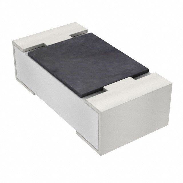
| 产品图片 |
|
| rohs | 符合RoHS无铅 / 符合限制有害物质指令(RoHS)规范要求 |
| 产品系列 | 时钟和计时器IC,时钟缓冲器,Micrel PL123-05NSC-R- |
| 数据手册 | |
| 产品型号 | PL123-05NSC-R |
| 产品种类 | 时钟缓冲器 |
| 供应商器件封装 | 8-SOP |
| 其它名称 | 576-4087-6 |
| 包装 | Digi-Reel® |
| 商标 | Micrel |
| 安装类型 | 表面贴装 |
| 安装风格 | SMD/SMT |
| 封装 | Reel |
| 封装/外壳 | 8-SOIC(0.154",3.90mm 宽) |
| 封装/箱体 | SOP-8 |
| 工作温度 | 0°C ~ 70°C |
| 工厂包装数量 | 2500 |
| 差分-输入:输出 | 无/无 |
| 标准包装 | 1 |
| 比率-输入:输出 | 1:5 |
| 电压-电源 | 1.62 V ~ 3.63 V |
| 电路数 | 1 |
| 类型 | 扇出缓冲器(分配) |
| 系列 | PL123-05 |
| 输入 | 时钟 |
| 输出 | 时钟 |
| 频率-最大值 | 134MHz |


- 商务部:美国ITC正式对集成电路等产品启动337调查
- 曝三星4nm工艺存在良率问题 高通将骁龙8 Gen1或转产台积电
- 太阳诱电将投资9.5亿元在常州建新厂生产MLCC 预计2023年完工
- 英特尔发布欧洲新工厂建设计划 深化IDM 2.0 战略
- 台积电先进制程称霸业界 有大客户加持明年业绩稳了
- 达到5530亿美元!SIA预计今年全球半导体销售额将创下新高
- 英特尔拟将自动驾驶子公司Mobileye上市 估值或超500亿美元
- 三星加码芯片和SET,合并消费电子和移动部门,撤换高东真等 CEO
- 三星电子宣布重大人事变动 还合并消费电子和移动部门
- 海关总署:前11个月进口集成电路产品价值2.52万亿元 增长14.8%


PDF Datasheet 数据手册内容提取
PL123-05N/-09N Low Skew Fanout Buffer FEATURES DESCRIPTION Output fanout buffer for DC to 134MHz The PL123-05N and PL123-09N are a low-cost Output Options: fanout buffers for distributing high-speed clocks with o 1:5 output fanout with PL123-05 low output to output skew and preserving low noise o 1:9 output fanout with PL123-09 properties. The fanout buffers accept an input from Low power consumption for portable applications DC to 134MHz and provide 5 or 9 outputs of the same Low input-output delay frequency. A typical PL123-09N application for driving Output-Output skew less than 250ps SDRAM in PC systems would use eight outputs to Low Additive Phase Jitter of 60fs RMS drive two DIMMs, or four SO-DIMMs, with the re- 2.5V to 3.3V, ±10% operation maining output used for driving an external feed- 1.8V ±10% operation up to 67MHz back to a PLL. A typical PL123-05N application is Operating temperature range from -40°C to 85°C to fanout a low noise CMOS clock oscillator to 5 Available in 16-Pin SOP (PL123-09) and 8-Pin low noise CMOS clocks. SOP (PL123-05). Both are GREEN/RoHS packag- es. These parts are not intended for 5V input-tolerant ap- plications. BLOCK DIAGRAM AND PACKAGE PINOUT CLK1 CLK2 REF 1 PL 8 CLK5 REF CLK3 CLK1 2 123 7 CLK4 CLK2 3 - 6 VDD 0 CLK4 GND 4 5N 5 CLK3 CLK5 SOP-8L CLK1 REF 1 16 CLK9 CLK2 CLK1 2 15 CLK8 CLK3 CLK2 3 P 14 CLK7 CLK4 VDD 4 L1 13 VDD 2 REF CLK5 GND 5 3- 12 GND 0 CLK3 6 9 11 CLK6 CLK6 N CLK4 7 10 CLK5 CLK7 VDD 8 9 GND CLK8 SOP-16L CLK9 Micrel Inc. • 2180 Fortune Drive • San Jose, CA 95131 • USA • tel +1(408) 944-0800 • fax +1(408) 474-1000 • www.micrel.com Rev 03/15/12 Page 1
PL123-05N/-09N Low Skew Fanout Buffer PIN DESCRIPTIONS PL123-09N PL123-05N Name Type Description SOP-16L SOP-8L REF 1 1 I Input reference frequency. CLK1 2 2 O Buffered clock output CLK2 3 3 O Buffered clock output VDD 4, 8, 13 6 P VDD connection GND 5, 9, 12 4 P GND connection CLK3 6 5 O Buffered clock output CLK4 7 7 O Buffered clock output CLK5 10 8 O Buffered clock output CLK6 11 - O Buffered clock output CLK7 14 - O Buffered clock output CLK8 15 - O Buffered clock output CLK9 16 - O Buffered clock output LAYOUT RECOMMENDATIONS The following guidelines are to assist you with a performance optimized PCB design: Signal Integrity and Termination Decoupling and Power Supply Considerations Considerations - Keep traces short! - Place decoupling capacitors as close as possible - Trace = Inductor. With a capacitive load this equals to the VDD pin(s) to limit noise from the power supply ringing! - Addition of a ferrite bead in series with VDD can - Long trace = Transmission Line. Without proper termi- help prevent noise from other board sources nation this will cause reflections ( looks like ringing ). - Value of decoupling capacitor is frequency de- - Design long traces (> 1 inch) as “striplines” or pendant. Typical values to use are 0.1F for de- “microstrips” with defined impedance. signs using frequencies < 50MHz and 0.01F for - Match trace at one side to avoid reflections bouncing designs using frequencies > 50MHz. back and forth. Typical CMOS termination Place Series Resistor as close as possible to CMOS output CMOS Output Buffer To CMOS Input ( Typical buffer impedance 20 ohm) 50 ohm line Connect a 33 ohm series resistor at each of the output clocks to enhance the stability of the output signal Micrel Inc. • 2180 Fortune Drive • San Jose, CA 95131 • USA • tel +1(408) 944-0800 • fax +1(408) 474-1000 • www.micrel.com Rev 03/15/12 Page 2
PL123-05N/-09N Low Skew Fanout Buffer ABSOLUTE MAXIMUM CONDITIONS Supply Voltage to Ground Potential ...... –0.5V to 4.6V Junction Temperature………………………….. 150°C DC Input Voltage ............................ V – 0.5V to 4.6V Static Discharge Voltage SS Storage Temperature ..........................–65°C to 150°C (per MIL-STD-883, Method 3015)…………..> 2000V OPERATING CONDITIONS Parameter Description Min. Max. Unit V Supply Voltage 1.62 3.63 V DD Commercial Operating Temperature (ambient temperature) 0 70 C T A Industrial Operating Temperature (ambient temperature) -40 85 C Load Capacitance, below 100 MHz, V > 2.25V ― 30 pF DD C Load Capacitance, above 100 MHz, V > 2.25V ― 10 pF L DD Load Capacitance, below 67MHz, 1.62V < V < 2.25V ― 15 pF DD C Input Capacitance ― 7 pF IN Operating Frequency, Input=Output, V > 2.25V DC 134 MHz DD REF, CLK[1:9] Operating Frequency, Input=Output, 1.62V < V < 2.25V DC 67 MHz DD Power-up time for all V s to reach minimum specified voltage t DD 0.05 50 ms PU (power ramps must be monotonic) Micrel Inc. • 2180 Fortune Drive • San Jose, CA 95131 • USA • tel +1(408) 944-0800 • fax +1(408) 474-1000 • www.micrel.com Rev 03/15/12 Page 3
PL123-05N/-09N Low Skew Fanout Buffer ELECTRICAL CHARACTERISTICS (Commercial and Industrial Temperature Devices) Parameter Description Test Conditions Min. Max. Unit V Input LOW Voltage [1] V > 2.25V – 0.8 V IL DD V Input HIGH Voltage [1] V > 2.25V 2.0 – V IH DD I Input LOW Current V = 0V – 50 µA IL IN I Input HIGH Current V = V – 100 µA IH IN DD V Output LOW Voltage [2] I = 8 mA , V > 2.97V – 0.4 V OL OL DD V Output HIGH Voltage [2] I = –8 mA , V > 2.97V 2.4 – V OH OH DD I Supply Current 66.67MHz with unloaded outputs – 32 mA DD SWITCHING CHARACTERISTICS (Commercial and Industrial Temperature Devices) [3] Parameter Description Test Conditions Min. Typ. Max. Unit Measured at 1.4V, V =3.3V, Input=50% 40 50 60 % DD Duty Cycle [2] = t2 ÷ t1 Measured at V /2 , Input = 50% 40 50 60 % DD 0.8V 2.0V , V =3.3V , 30pF Load – – 1.5 ns DD t Rise Time [2] 10% 90% , V =2.5V , 15pF Load – – 2.5 ns 3 DD 10% 90% , V =1.8V , 15pF Load – – 4.5 ns DD t Fall Time [2] 2.0V 0.8V , V =3.3V , 30pF Load – – 1.5 ns 4 DD 90% 10% , V =2.5V , 15pF Load – – 2.5 ns DD 90% 10% , V =1.8V , 15pF Load – – 4.5 ns DD t Output to Output Skew [2] All outputs equally loaded – – 250 ps 5 Propagation Delay, REF Rising t Measured at V /2 1 5 9.2 ns 6 Edge to CLKX Rising Edge [2] DD Notes: 1. REF input has a threshold voltage of V /2 DD 2. Parameter is guaranteed by design and characterization. Not 100% tested in production. 3. All parameters are specified with loaded outputs. Micrel Inc. • 2180 Fortune Drive • San Jose, CA 95131 • USA • tel +1(408) 944-0800 • fax +1(408) 474-1000 • www.micrel.com Rev 03/15/12 Page 4
PL123-05N/-09N Low Skew Fanout Buffer NOISE CHARACTERISTICS (Commercial and Industrial Temperature Devices) Parameter Description Test Conditions Min. Typ. Max. Unit V =3.3V, Frequency=100MHz Additive Phase Jitter DD 60 fs Offset=12KHz ~ 20MHz PL123-09N Additive Phase Jitter: VDD=3.3V, CLK=100MHz, Integration Range 12KHz to 20MHz: 0.059ps typical. REF Input PL123-09N Output -60 -70 -80 -90 z) H c/ -100 B d se ( -110 oi N e s -120 a h P -130 -140 -150 -160 10 100 1000 10000 100000 1000000 10000000 100000000 Offset Frequency (Hz) When a buffer is used to pass a signal then the buffer will add a little bit of its own noise. The phase noise on the output of the buffer will be a little bit more than the phase noise in the input signal. To quantify the noise addition in the buffer we compare the Phase Jitter numbers from the input and the output. The difference is called "Additive Phase Jitter". The formula for the Additive Phase Jitter is as follows: 2 2 Additive Phase Jitter = (Output Phase Jitter) - (Input Phase Jitter) Micrel Inc. • 2180 Fortune Drive • San Jose, CA 95131 • USA • tel +1(408) 944-0800 • fax +1(408) 474-1000 • www.micrel.com Rev 03/15/12 Page 5
PL123-05N/-09N Low Skew Fanout Buffer SWITCHING WAVEFORMS Duty Cycle Timing t 1 t 2 1.4V 1.4V All Outputs Rise/Fall Time 2.0V 2.0V 3.3V V 0.8V 0.8V OUTPUT 0V t t 3 4 Output-Output Skew 1.4V OUTPUT 1.4V OUTPUT t 5 Input-Output Propagation Delay VDD/2 INPUT VDD/2 OUTPUT t 6 TEST CIRCUIT VDD 0.1 F CLK OUTPUTS C LOAD VDD 0.1 F GND GND Micrel Inc. • 2180 Fortune Drive • San Jose, CA 95131 • USA • tel +1(408) 944-0800 • fax +1(408) 474-1000 • www.micrel.com Rev 03/15/12 Page 6
PL123-05N/-09N Low Skew Fanout Buffer PACKAGE DRAWING (GREEN PACKAGE COMPLIANT) SOP-16L ( mm ) Symbol Min. Max. E H A 1.35 1.75 A1 0.10 0.25 B 0.33 0.51 D C 0.19 0.25 D 9.80 10.00 E 3.80 4.00 H 5.80 6.20 L 0.40 1.27 A e 1.27 BSC A1 C L B e SOP-8L (mm) Symbol Min. Max. A 1.35 1.75 A1 0.10 0.25 E H A2 1.25 1.50 B 0.33 0.53 C 0.19 0.27 D 4.80 5.00 D E 3.80 4.00 H 5.80 6.20 L 0.40 0.89 e 1.27 BSC A2 A A1 C b L e Micrel Inc. • 2180 Fortune Drive • San Jose, CA 95131 • USA • tel +1(408) 944-0800 • fax +1(408) 474-1000 • www.micrel.com Rev 03/15/12 Page 7
PL123-05N/-09N Low Skew Fanout Buffer ORDERING INFORMATION For part ordering, please contact our Sales Department: 2180 Fortune Drive, San Jose, CA 95131, USA Tel: (408) 944-0800 Fax: (408) 474-1000 PART NUMBER The order number for this device is a combination of the following: Part number, Package type and Operating temperature range PL123-0xN X X - X None=Tubes Part Number R=Tape & Reel Package Type Temperature Range S=SOP C=Commercial (0°C to 70°C) I=Industrial (-40°C to 85°C) Part/Order Number Marking Package Option Green (Lead-Free) Package PL123-09NSC P12309N 16-Pin SOP Tube SC PL123-09NSC-R 16-Pin SOP (Tape and Reel) LLLLL P12309N PL123-09NSI 16-Pin SOP Tube SI PL123-09NSI-R LLLLL 16-Pin SOP (Tape and Reel) PL123-05NSC P12305N 8-Pin SOP Tube SC PL123-05NSC-R LLLLL 8-Pin SOP (Tape and Reel) P12305N PL123-05NSI 8-Pin SOP Tube SI PL123-05NSI-R 8-Pin SOP (Tape and Reel) LLLLL *Note: LLLLL designates lot number Micrel Inc., reserves the right to make changes in its products or specifications, or both at any time without notice. The information furnished by Micrel is believed to be accurate and reliable. However, Micrel makes no guarantee or warranty concerning the accuracy of said information and shall not be responsible for any loss or damage of whatever nature resulting from the use of, or reliance upon this product. LIFE SUPPORT POLICY: Micrel’s products are not authorized for use as critical components in life support devices or systems without the express written approval of the President of Micrel Inc. Micrel Inc. • 2180 Fortune Drive • San Jose, CA 95131 • USA • tel +1(408) 944-0800 • fax +1(408) 474-1000 • www.micrel.com Rev 03/15/12 Page 8