ICGOO在线商城 > 集成电路(IC) > 嵌入式 - 微控制器 > PIC18F65J94-I/PT

 Datasheet下载
- 型号: PIC18F65J94-I/PT
- 制造商: Microchip
- 库位|库存: xxxx|xxxx
- 要求:
| 数量阶梯 | 香港交货 | 国内含税 |
| +xxxx | $xxxx | ¥xxxx |
查看当月历史价格
查看今年历史价格
PIC18F65J94-I/PT产品简介:
ICGOO电子元器件商城为您提供PIC18F65J94-I/PT由Microchip设计生产,在icgoo商城现货销售,并且可以通过原厂、代理商等渠道进行代购。 PIC18F65J94-I/PT价格参考。MicrochipPIC18F65J94-I/PT封装/规格:嵌入式 - 微控制器, PIC 微控制器 IC PIC® XLP™ 18J 8-位 64MHz 32KB(16K x 16) 闪存 64-TQFP(10x10)。您可以下载PIC18F65J94-I/PT参考资料、Datasheet数据手册功能说明书,资料中有PIC18F65J94-I/PT 详细功能的应用电路图电压和使用方法及教程。
| 参数 | 数值 |
| A/D位大小 | 12 bit |
| 产品目录 | 集成电路 (IC)半导体 |
| 描述 | IC MCU 8BIT 32KB FLASH 64TQFP8位微控制器 -MCU 64 pins, 32KB Flash 4KB RAM, 16MIPS |
| EEPROM容量 | - |
| 产品分类 | |
| I/O数 | 52 |
| 品牌 | Microchip Technology |
| 产品手册 | |
| 产品图片 |
|
| rohs | 符合RoHS无铅 / 符合限制有害物质指令(RoHS)规范要求 |
| 产品系列 | 嵌入式处理器和控制器,微控制器 - MCU,8位微控制器 -MCU,Microchip Technology PIC18F65J94-I/PTPIC® XLP™ 18J |
| 数据手册 | http://www.microchip.com/mymicrochip/filehandler.aspx?ddocname=en559951http://www.microchip.com/mymicrochip/filehandler.aspx?ddocname=en560103 |
| 产品型号 | PIC18F65J94-I/PT |
| PCN组件/产地 | 点击此处下载产品Datasheethttp://www.microchip.com/mymicrochip/NotificationDetails.aspx?id=5780&print=viewhttp://www.microchip.com/mymicrochip/NotificationDetails.aspx?id=5939&print=view |
| PCN设计/规格 | |
| RAM容量 | 4K x 8 |
| 产品种类 | 8位微控制器 -MCU |
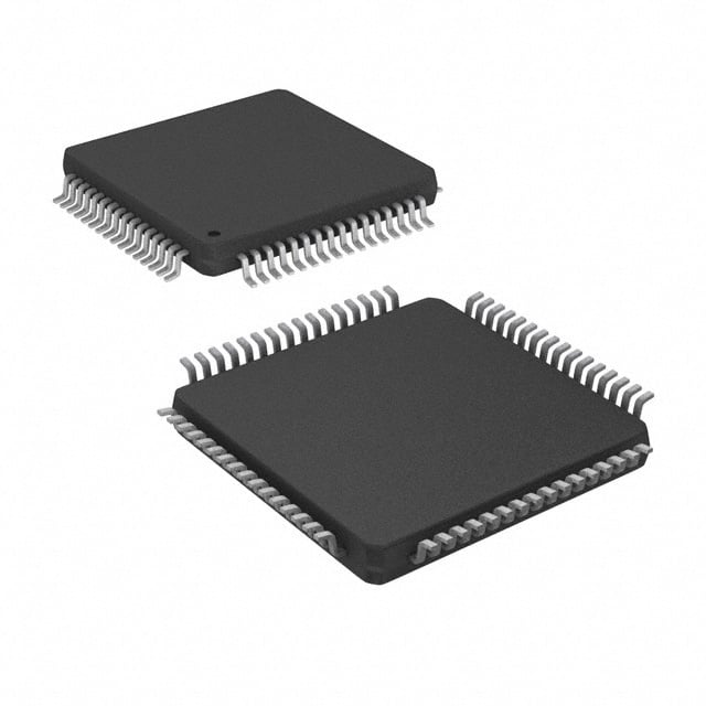
| 供应商器件封装 | 64-TQFP(10x10) |
| 包装 | 托盘 |
| 可用A/D通道 | 16 |
| 商标 | Microchip Technology |
| 外设 | 欠压检测/复位,HLVD,LCD,POR,PWM,WDT |
| 安装风格 | SMD/SMT |
| 定时器数量 | 4 |
| 封装 | Tray |
| 封装/外壳 | 64-TQFP |
| 封装/箱体 | TQFP-64 |
| 工作温度 | -40°C ~ 85°C |
| 工作电源电压 | 2 V to 3.6 V |
| 工厂包装数量 | 160 |
| 振荡器类型 | 内部 |
| 接口类型 | I2C, SPI |
| 数据RAM大小 | 4 kB |
| 数据Ram类型 | SRAM |
| 数据总线宽度 | 8 bit |
| 数据转换器 | A/D 16x10b/12b |
| 最大工作温度 | + 85 C |
| 最大时钟频率 | 64 MHz |
| 最小工作温度 | - 40 C |
| 标准包装 | 160 |
| 核心 | PIC |
| 核心处理器 | PIC |
| 核心尺寸 | 8-位 |
| 片上ADC | Yes |
| 片上DAC | No |
| 电压-电源(Vcc/Vdd) | 2 V ~ 3.6 V |
| 电源电压-最大 | 3.6 V |
| 电源电压-最小 | 2 V |
| 程序存储器大小 | 32 kB |
| 程序存储器类型 | Flash |
| 程序存储容量 | 32KB(16K x 16) |
| 连接性 | I²C, IrDA, LIN, SPI, UART/USART, USB |
| 速度 | 64MHz |


- 商务部:美国ITC正式对集成电路等产品启动337调查
- 曝三星4nm工艺存在良率问题 高通将骁龙8 Gen1或转产台积电
- 太阳诱电将投资9.5亿元在常州建新厂生产MLCC 预计2023年完工
- 英特尔发布欧洲新工厂建设计划 深化IDM 2.0 战略
- 台积电先进制程称霸业界 有大客户加持明年业绩稳了
- 达到5530亿美元!SIA预计今年全球半导体销售额将创下新高
- 英特尔拟将自动驾驶子公司Mobileye上市 估值或超500亿美元
- 三星加码芯片和SET,合并消费电子和移动部门,撤换高东真等 CEO
- 三星电子宣布重大人事变动 还合并消费电子和移动部门
- 海关总署:前11个月进口集成电路产品价值2.52万亿元 增长14.8%


PDF Datasheet 数据手册内容提取
PIC18F97J94 FAMILY 8-Bit LCD Flash Microcontroller with USB and XLP Technology eXtreme Low-Power Features • Hardware Real-Time Clock/Calendar (RTCC): - Runs in Deep Sleep and VBAT modes • Multiple Power Management Options for Extreme • Two Master Synchronous Serial Ports (MSSP) Power Reduction: modules Featuring: - VBAT allows for lowest power consumption on - 3-Wire/4-Wire SPI (all 4 modes) back-up battery (with or without RTCC) - SPI Direct Memory Access (DMA) channel - Deep Sleep allows near total power-down with the w/1024 byte count ability to wake-up on external triggers - Two I2C modules Support Multi-Master/Slave - Sleep and Idle modes selectively shut down mode and 7-Bit/10-Bit Addressing peripherals and/or core for substantial power • Four Enhanced Addressable USART modules: reduction and fast wake-up - Support RS-485, RS-232 and LIN/J2602 • Alternate Clock modes Allow On-the-Fly Switching to - On-chip hardware encoder/decoder for IrDA® a Lower Clock Speed for Selective Power Reduction - Auto-wake-up on Auto-Baud Detect • Extreme Low-Power Current Consumption for • Digital Signal Modulator Provides On-Chip OOK, Deep Sleep: FSK and PSK Modulation for a Digital Signal Stream - WDT: 650nA @ 2V typical • High-Current Sink/Source 18 mA/18 mA on all Digital I/O - RTCC: 650nA @ 32 kHz, 2V typical • Configurable Open-Drain Outputs on ECCP/CCP/ - Deep Sleep current, 80nA typical USART/MSSP • Extended Microcontroller mode Using 12, 16 or Universal Serial Bus Features 20-Bit Addressing mode • USB V2.0 Compliant Analog Features • Low Speed (1.5 Mb/s) and Full Speed (12 Mb/s) • Supports Control, Interrupt, Isochronous and Bulk • 10/12-Bit, 24-Channel Analog-to-Digital (A/D) Transfers Converter: • Supports up to 32 Endpoints (16 bidirectional) - Conversion rate of 500ksps (10-bit), • USB module can use Any RAM Location on the 200kbps (12-bit) Device as USB Endpoint Buffers - Conversion available during Sleep and Idle • On-Chip USB Transceiver • Three Rail-to-Rail Enhanced Analog Comparators with Programmable Input/Output Configuration Peripheral Features • On-Chip Programmable Voltage Reference • Charge Time Measurement Unit (CTMU): • LCD Display Controller: - Used for capacitive touch sensing, up to - Up to 60 segments by 8 commons 24 channels - Internal charge pump and low-power, internal - Time measurement down to 1ns resolution resistor biasing - CTMU temperature sensing - Operation in Sleep mode • Up to Four External Interrupt Sources • Peripheral Pin Select Lite (PPS-Lite): High-Performance CPU - Allows independent I/O mapping of many peripherals • High-Precision PLL for USB • Four 16-Bit and Four 8-Bit Timers/Counters with • Two External Clock modes, Up to 64MHz Prescaler (16 MIPS®) • Seven Capture/Compare/PWM (CCP) modules • Internal 31kHz Oscillator • Three Enhanced Capture/Compare/PWM (ECCP) • High-Precision Internal Oscillator with Clock modules: Recovery from SOSC to Achieve 0.15% Precision, - One, two or four PWM outputs 31 kHz to 8 MHz or 64 MHz w/PLL, - Selectable polarity ±0.15% Typical, ±1.5% Max. - Programmable dead time • Secondary Oscillator using Timer1 @ 32 kHz - Auto-shutdown and auto-restart • C Compiler Optimized Instruction Set Architecture - Pulse steering control • Two Address Generation Units for Separate Read and Write Addressing of Data Memory 2012-2016 Microchip Technology Inc. DS30000575C-page 1
PIC18F97J94 FAMILY Special Microcontroller Features • Power-on Reset (POR), Power-up Timer (PWRT) and Oscillator Start-up Timer (OST) • Operating Voltage Range of 2.0V to 3.6V • Brown-out Reset (BOR) with Operation Below VBOR, • Two On-Chip Voltage Regulators (1.8V and 1.2V) for with Regulator Enabled Regular and Extreme Low-Power Operation • High/Low-Voltage Detect (HLVD) • 20,000 Erase/Write Cycle Endurance Flash Program • Flexible Watchdog Timer (WDT) with its Own Memory, Typical RC Oscillator for Reliable Operation • Flash Data Retention: 10 Years Minimum • Standard and Ultra Low-Power Watchdog Timers • Self-Programmable under Software Control (WDT) for Reliable Operation in Standard and Deep • Two Configurable Reference Clock Outputs Sleep modes (REFO1 and REFO2) • In-Circuit Serial Programming™ (ICSP™) • Fail-Safe Clock Monitor Operation: - Detects clock failure and switches to on-chip, low-power RC oscillator TABLE 1: PIC18F97J94 FAMILY TYPES Device Pins Flash MPrograme(bytes)morData SRAMy(bytes) Timers 8-Bit/16-BitRem®aUSART w/IrDAppableSPI w/ DMA PeriphComparatorserals CCP/ECCP 2IC 10/12-Bit A/D (ch) CTMU LCD (pixels) USB Deep Sleep w/VBAT PPS (Lite) PIC18F97J94 100 128K 4K 4 4 2 3 Y 2 24 Y 480 Y Y Lite PIC18F87J94 80 128K 4K 4 4 2 3 Y 2 24 Y 352 Y Y Lite PIC18F67J94 64 128K 4K 4 4 2 3 Y 2 16 Y 224 Y Y Lite PIC18F96J94 100 64K 4K 4 4 2 3 Y 2 24 Y 480 Y Y Lite PIC18F86J94 80 64K 4K 4 4 2 3 Y 2 24 Y 352 Y Y Lite PIC18F66J94 64 64K 4K 4 4 2 3 Y 2 16 Y 224 Y Y Lite PIC18F95J94 100 32K 4K 4 4 2 3 Y 2 24 Y 480 Y Y Lite PIC18F85J94 80 32K 4K 4 4 2 3 Y 2 24 Y 352 Y Y Lite PIC18F65J94 64 32K 4K 4 4 2 3 Y 2 16 Y 224 Y Y Lite For other small form-factor package availability and marking information, visit http://www.microchip.com/packaging or contact your local sales office. DS30000575C-page 2 2012-2016 Microchip Technology Inc.
PIC18F97J94 FAMILY PIN DIAGRAMS FIGURE 1: 64-PIN TQFP, QFN DIAGRAM FOR PIC18F6XJ94 7 56D DDR P30/CS/RE2REFO1/RE3RE4RE5RE6P31/RE7PSP0/RD0 PSP1/RD1PSP2/RD2PSP3/RD3PSP4/RD4RP25/PSP5/RRP26/PSP6/RREFO2/PSP7/ AS3/RRP33/RP32/RP37/RP34/AS0/RRP20/ RP21/RP22/RP23/RP24/SDA2/SCL2/RP27/ CDBIOM0/OM1/OM2/OM3/CDBIEG0/DD SSEG1/EG2/EG3/EG4/EG5/EG6/EG7/ LCCCCLSVVSSSSSSS 4321098765432109 6666655555555554 LCDBIAS2/RP29/WR/RE1 1 48 VLCAP1/RP8/CTED13/INT0/RB0 LCDBIAS1/RP28/RD/RE0 2 47 VLCAP2/RP9/RB1 COM4/SEG28/AN8/RP46/RG0 3 46 SEG9/RP14/CTED1/RB2 COM5/SEG29/AN19/RP39/RG1 4 45 SEG10/RP7/CTED2/RB3 COM6/SEG30/AN18/C3INA/RP42/RG2 5 44 SEG11/RP12/CTED3/RB4 COM7/SEG31/AN17/C3INB/RP43/RG3 6 43 SEG8/RP13/CTED4/RB5 MCLR 7 42 CTED5/PGC/RB6 SEG26/AN16/C3INC/RP44/RTCC/RG4 8 PIC18F6XJ94 41 VSS VSS 9 40 OSC2/CLKO/RP6/RA6 VCAP 10 39 OSC1/CLKI/RP10/RA7 SEG25/AN5/RP38/RF7 11 38 VDD SEG24/AN11/C1INA/RP40/RF6 12 37 CTED6/PGD/RB7 SEG23/CVREF/AN10/C1INB/RP35/RF5 13 36 SEG12/RP16/CTED10/RC5 D+/RF4 14 35 SEG16/SDA1/RP17/CTED9/RC4 D-/RF3 15 34 SEG17/SCL1/RP15/CTED8/RC3 SEG20/AN7/CTMUI/C2INB/RP36/RF2 16 33 SEG13/AN9/RP11/CTED7/RC2 7890123456789012 1112222222222333 V33USBVVBATAVDDAVSSRP3/RA3RP2/RA2RP1/RA1RP0/RA0VSSVDDRP5/RA5RP4/RA4SCI/RC1CLK/RC0D11/RC6D12/RC7 V+/AN3/REFSEG21/V-/AN2/REFSEG18/AN1/SEG19/AN0/AN1-/ N/C1INA/C2INA/C3INA/SEG14/AN6/SOSOSCO/SCLKI/PWRLSEG27/RP18/UOE/CTESEG22/RP19/CTE DI V L 4/ N A 5/ 1 G E S Note1: Pinouts are subject to change. 2: See Table2 for the pin allocation table. 2012-2016 Microchip Technology Inc. DS30000575C-page 3
PIC18F97J94 FAMILY FIGURE 2: 80-PIN TQFP DIAGRAM FOR PIC18F8XJ94 7 56D DDR S/RE21/RE3 E7D0 D1D2D3D4SP5/RSP6/RPSP7/ CO RR RRRRPP2/ A17/SEG46/AN22/RH1A16/SEG47/AN23/RH0AD10/LCDBIAS3/RP30/AD11/COM0/RP33/REFAD12/COM1/RP32/RE4AD13/COM2/RP37/RE5AD14/COM3/RP34/RE6AD15/LCDBIAS0/RP31/AD0/SEG0/RP20/PSP0/VDDVSSAD1/SEG1/RP21/PSP1/AD2/SEG2/RP22/PSP2/AD3/SEG3/RP23/PSP3/AD4/SEG4/RP24/PSP4/AD5/SEG5/SDA2/RP25/AD6/SEG6/SCL2/RP26/AD7/SEG7/RP27/REFOALE/SEG32/RJ0OE/SEG33/RJ1 09876543210987654321 87777777777666666666 A18/SEG45/AN21/RH2 1 60 WRL/SEG34/RJ2 A19/SEG44/AN20/RH3 2 59 WRH/SEG35/RJ3 AD9/LCDBIAS2/RP29/WR/RE1 3 58 VLCAP1/RP8/CTED13/INT0/RB0 AD8/LCDBIAS1/RP28/RD/RE0 4 57 VLCAP2/RP9/RB1 COM4/SEG28/AN8/RP46/RG0 5 56 SEG9/RP14/CTED1/RB2 COM5/SEG29/AN19/RP39/RG1 6 55 SEG10/RP7/CTED2/RB3 COM6/SEG30/AN18/C3INA/RP42/RG2 7 54 SEG11/RP12/CTED3/RB4 COM7/SEG31/AN17/C3INB/RP43/RG3 8 53 SEG8/RP13/CTED4/RB5 MCLR 9 52 CTED5/PGC/RB6 SEG26/AN16/C3INC/RP44/RTCC/RG4 10 PIC18F8XJ94 51 VSS VSS 11 50 OSC2/CLKO/RP6/RA6 VCAP 12 49 OSC1/CLKI/RP10/RA7 SEG25/AN5/RP38/RF7 13 48 VDD SEG24/AN11/C1INA/RP40/RF6 14 47 CTED6/PGD/RB7 SEG23/CVREF/AN10/C1INB/RP35/RF5 15 46 SEG12/RP16/CTED10/RC5 D+/RF4 16 45 SEG16/SDA1/RP17/CTED9/RC4 D-/RF3 17 44 SEG17/SCL1/RP15/CTED8/RC3 SEG20/AN7/C2INB/RP36/RF2 18 43 SEG13/AN9/RP11/CTED7/RC2 SEG43/AN15/RH7 19 42 UB/SEG36/RJ7 SEG42/AN14/C1INC/RH6 20 41 LB/SEG37/RJ6 12345678901234567890 22222222233333333334 SEG41/AN13/C2IND/RH5SEG40/AN12/C2INC/RH4V33USBVVBATAVDDAVSSV+/AN3/RP3/RA3REFSEG21/V-/AN2/RP2/RA2REFSEG18/AN1/RP1/RA1SEG19/AN0/AN1-/RP0/RA0VssVDDN/C1INA/C2INA/C3INA/RP5/RA5SEG14/AN6/RP4/RA4SOSCI/RC1SOSCO/SCLKI/PWRLCLK/RC0SEG27/RP18/UOE/CTED11/RC6SEG22/RP19/CTED12/RC7BA0/SEG39/RJ4CE/SEG38/RJ5 DI V L 4/ N A 5/ 1 G E S Note1: Pinouts are subject to change. 2: See Table3 for the pin allocation table. DS30000575C-page 4 2012-2016 Microchip Technology Inc.
PIC18F97J94 FAMILY FIGURE 3: 100-PIN TQFP DIAGRAM FOR PIC18F9XJ94 7 5 6D D DR S/RE21/RE3 E7 D0 D1 D2D3D4SP5/R SP6/RPSP7/ CO R R R RRRP P2/ A17/SEG46/AN22/RH1A16/SEG47/AN23/RH0AD10/LCDBIAS3/RP30/AD11/COM0/RP33/REFRG7AD12/COM1/RP32/RE4AD13/COM2/RP37/RE5AD14/COM3/RP34/RE6AD15/LCDBIAS0/RP31/SEG48/RL0AD0/SEG0/RP20/PSP0/RG6VDDVSSAD1/SEG1/RP21/PSP1/SEG63/RK7AD2/SEG2/RP22/PSP2/AD3/SEG3/RP23/PSP3/AD4/SEG4/RP24/PSP4/AD5/SEG5/SDA2/RP25/SEG62/RK6AD6/SEG6/SCL2/RP26/AD7/SEG7/RP27/REFOALE/SEG32/RJ0OE/SEG33/RJ1 00999897969594939291908988878685848382818079787776 A18/SEG45/AN21/RH2 11 75 WRL/SEG34/RJ2 A19/SEG44/AN20/RH3 2 74 WRH/SEG35/RJ3 AD9/LCDBIAS2/RP29/WR/RE1 3 73 VLCAP1/RP8/CTED13/INT0/RB0 AD8/LCDBIAS1/RP28/RD/RE0 4 72 VLCAP2/RP9/RB1 VDD 5 71 DDIO1/SEG61/RK5 COM4/SEG28/AN8/RP46/RG0 6 70 SEG9/RP14/CTED1/RB2 COM5/SEG29/AN19/RP39/RG1 7 69 SEG10/RP7/CTED2/RB3 COM6/SEG30/AN18/C3INA/RP42/RG2 8 68 SEG11/RP12/CTED3/RB4 COM7/SEG31/AN17/C3INB/RP43/RG3 9 67 SEG8/RP13/CTED4/RB5 SEG49/RL1 10 66 DDIO0/SEG60/RK4 MCLR 11 65 CTED5/PGC/RB6 SEG26/AN16/C3INC/RP44/RTCC/RG4 12 PIC18F9XJ94 64 VSS SEG50/RL2 13 63 SEG59/RK3 VSS 14 62 OSC2/CLKO/RP6/RA6 VCAP 15 61 OSC1/CLKI/RP10/RA7 SEG51/RL3 16 60 SEG58/RK2 SEG25/AN5/RP38/RF7 17 59 VDD SEG24/AN11/C1INA/RP40/RF6 18 58 CTED6/PGD/RB7 SEG23/CVREF/AN10/C1INB/RP35/RF5 19 57 SEG12/RP16/CTED10/RC5 D+/RF4 20 56 SEG16/SDA1/RP17/CTED9/RC4 SEG52/RL4 21 55 SEG57/RK1 D-/RF3 22 54 SEG17/SCL1/RP15/CTED8/RC3 SEG20/AN7/CTMUI/C2INB/RP36/RF2 23 53 SEG13/AN9/RP11/CTED7/RC2 SEG43/AN15/RH7 24 52 UB/SEG36/RJ7 SEG42/AN14/C1INC/RH6 25 51 LB/SEG37/RJ6 6789012345678901234567890 2222333333333344444444445 543T5DS32S106SD7541006745 SEG41/AN13/C2IND/RHSEG40/AN12/C2INC/RHV3USBVVBASEG53/RLAVDAVSV+/AN3/RP3/RAREFSEG21/V-/AN2/RP2/RAREFVSSEG18/AN1/RP1/RASEG19/AN0/AN1-/RP0/RASEG54/RLVSVDSEG55/RLN/C1INA/C2INA/C3INA/RP5/RASEG14/AN6/RP4/RASOSCI/RCSOSCO/SCLKI/PWRLCLK/RCSEG56/RKSEG27/RP18/UOE/CTED11/RCSEG22/RP19/CTED12/RCBA0/SEG39/RJCE/SEG38/RJ DI V L 4/ N A 5/ 1 G E S Note1: Pinouts are subject to change. 2: See Table4 for the pin allocation table. 2012-2016 Microchip Technology Inc. DS30000575C-page 5
PIC18F97J94 FAMILY PIN ALLOCATION TABLES TABLE 2: 64-PIN ALLOCATION TABLE (PIC18F6XJ94) N F I/O Pin TQFP/Q ADC Comparator HLVD CTMU USB LCD MSSP PSP Interrupt REFO (1)PPS-Lite Pull-up Basic - 4 6 RA0 24 AN0/ — — — — SEG19 — — — — RP0 — — AN1- RA1 23 AN1 — — — — SEG18 — — — — RP1 — — RA2 22 AN2/ — — — — SEG21 — — — — RP2 — — VREF- RA3 21 AN3/ — — — — — — — — — RP3 — — VREF+ RA4 28 AN6 — — — — SEG14 — — — — RP4 — — RA5 27 AN4 C1INA/ LVDIN — — SEG15 — — — — RP5 — — C2INA/ C3INA RA6 40 — — — — — — — — — — RP6 — OSC2/ CLKO RA7 39 — — — — — — — — — — RP10 — OSC1/ CLKI RB0 48 — — — CTED13 — VLCAP1 — — INT0 — RP8 — — RB1 47 — — — — — VLCAP2 — — — — RP9 — — RB2 46 — — — CTED1 — SEG9 — — — — RP14 — — RB3 45 — — — CTED2 — SEG10 — — — — RP7 — — RB4 44 — — — CTED3 — SEG11 — — — — RP12 — — RB5 43 — — — CTED4 — SEG8 — — — — RP13 — — RB6 42 — — — CTED5 — — — — — — — — PGC RB7 37 — — — CTED6 — — — — — — — — PGD RC0 30 — — — — — — — — — — — — SOSCO/ SCKI/ PWRCLK RC1 29 — — — — — — — — — — — — SOSCI RC2 33 AN9 — — CTED7 — SEG13 — — — — RP11 — — RC3 34 — — — CTED8 — SEG17 SCL1 — — — RP15 — — RC4 35 — — — CTED9 — SEG16 SDA1 — — — RP17 — — RC5 36 — — — CTED10 — SEG12 — — — — RP16 — — RC6 31 — — — CTED11 UOE SEG27 — — — — RP18 — — RC7 32 — — — CTED12 — SEG22 — — — — RP19 — — RD0 58 — — — — — SEG0 — PSP0 — — RP20 Y — RD1 55 — — — — — SEG1 — PSP1 — — RP21 Y — RD2 54 — — — — — SEG2 — PSP2 — — RP22 Y — RD3 53 — — — — — SEG3 — PSP3 — — RP23 Y — RD4 52 — — — — — SEG4 — PSP4 — — RP24 Y — RD5 51 — — — — — SEG5 SDA2 PSP5 — — RP25 Y — RD6 50 — — — — — SEG6 SCL2 PSP6 — — RP26 Y — RD7 49 — — — — — SEG7 — PSP7 — REFO2 RP27 Y — RE0 2 — — — — — LCDBIAS1 — RD — — RP28 Y — RE1 1 — — — — — LCDBIAS2 — WR — — RP29 Y — RE2 64 — — — — — LCDBIAS3 — CS — — RP30 Y — RE3 63 — — — — — COM0 — — — REFO1 RP33 Y — RE4 62 — — — — — COM1 — — — — RP32 Y — RE5 61 — — — — — COM2 — — — — RP37 Y — DS30000575C-page 6 2012-2016 Microchip Technology Inc.
PIC18F97J94 FAMILY TABLE 2: 64-PIN ALLOCATION TABLE (PIC18F6XJ94) (CONTINUED) N F I/O Pin TQFP/Q ADC Comparator HLVD CTMU USB LCD MSSP PSP Interrupt REFO (1)PPS-Lite Pull-up Basic - 4 6 RE6 60 — — — — — COM3 — — — — RP34 Y — RE7 59 — — — — — LCDBIAS0 — — — — RP31 Y — RF2 16 AN7 C2INB — CTMUI — SEG20 — — — — RP36 Y — RF3 15 — — — — D- — — — — — — Y — RF4 14 — — — — D+ — — — — — — Y — RF5 13 AN10 C1INB/ — — — SEG23 — — — — RP35 Y — CVREF RF6 12 AN11 C1INA — — — SEG24 — — — — RP40 Y — RF7 11 AN5 — — — — SEG25 — — — — RP38 Y — RG0 3 AN8 — — — — COM4/ — — — — RP46 Y — SEG28 RG1 4 AN19 — — — — COM5/ — — — — RP39 Y — SEG29 RG2 5 AN18 C3INA — — — COM6/ — — — — RP42 Y — SEG30 RG3 6 AN17 C3INB — — — COM7/ — — — — RP43 Y — SEG31 RG4 8 AN16 C3INC — — — SEG26 — — — — RP44 Y — RG5/ 7 — — — — — — — — — — — Y MCLR MCLR AVDD 19 AVDD — — — — — — — — — — — — AVSS 20 AVSS — — — — — — — — — — — — VBAT 18 — — — — — — — — — — — — VBAT VCAP/ 10 — — — — — — — — — — — — VCAP/ VDDCORE VDDCORE VDD 26, — — — — — — — — — — — — VDD 38, 57 VSS 9, — — — — — — — — — — — — VSS 25, 41, 56 VUSB3V3 17 — — — — — — — — — — — — VUSB3V3 Note 1: The peripheral inputs and outputs that support PPS have no default pins. 2012-2016 Microchip Technology Inc. DS30000575C-page 7
PIC18F97J94 FAMILY TABLE 3: 80-PIN ALLOCATION TABLE (PIC18F8XJ94) I/O 80-Pin TQFP ADC Comparator HLVD CTMU USB LCD MSSP PSP Interrupt REFO EMB (1)PPS-Lite Pull-up Basic RA0 30 AN0/ — — — — SEG19 — — — — — RP0 — — AN1- RA1 29 AN1 — — — — SEG18 — — — — — RP1 — — RA2 28 AN2/ — — — — SEG21 — — — — — RP2 — — VREF- RA3 27 AN3/ — — — — — — — — — — RP3 — — VREF+ RA4 34 AN6 — — — — SEG14 — — — — — RP4 — — RA5 33 AN4 C1INA/ LVDIN — — SEG15 — — — — — RP5 — — C2INA/ C3INA RA6 50 — — — — — — — — — — — RP6 — OSC2/ CLKO RA7 49 — — — — — — — — — — — RP10 — OSC1/ CLKI RB0 58 — — — CTED13 — VLCAP1 — — INT0 — — RP8 — — RB1 57 — — — — — VLCAP2 — — — — — RP9 — — RB2 56 — — — CTED1 — SEG9 — — — — — RP14 — — RB3 55 — — — CTED2 — SEG10 — — — — — RP7 — — RB4 54 — — — CTED3 — SEG11 — — — — — RP12 — — RB5 53 — — — CTED4 — SEG8 — — — — — RP13 — — RB6 52 — — — CTED5 — — — — — — — — — PGC RB7 47 — — — CTED6 — — — — — — — — — PGD RC0 36 — — — — — — — — — — — — — SOSCO/ SCKI/ PWRCLK RC1 35 — — — — — — — — — — — — — SOSCI RC2 43 AN9 — — CTED7 — SEG13 — — — — — RP11 — — RC3 44 — — — CTED8 — SEG17 SCL1 — — — — RP15 — — RC4 45 — — — CTED9 — SEG16 SDA1 — — — — RP17 — — RC5 46 — — — CTED10 — SEG12 — — — — — RP16 RC6 37 — — — CTED11 UOE SEG27 — — — — — RP18 — — RC7 38 — — — CTED12 — SEG22 — — — — — RP19 — — RD0 72 — — — — — SEG0 — PSP0 — — AD0 RP20 Y — RD1 69 — — — — — SEG1 — PSP1 — — AD1 RP21 Y — RD2 68 — — — — — SEG2 — PSP2 — — AD2 RP22 Y — RD3 67 SEG3 PSP3 AD3 RP23 Y — RD4 66 — — — — — SEG4 — PSP4 — — AD4 RP24 Y — RD5 65 — — — — — SEG5 SDA2 PSP5 — — AD5 RP25 Y — RD6 64 — — — — — SEG6 SCL2 PSP6 — — AD6 RP26 Y — RD7 63 — — — — — SEG7 — PSP7 — REFO2 AD7 RP27 Y — RE0 4 — — — — — LCDBIAS1 — RD — — AD8 RP28 Y — RE1 3 — — — — — LCDBIAS2 — WR — — AD9 RP29 Y — RE2 78 — — — — — LCDBIAS3 — CS — — AD10 RP30 Y — RE3 77 — — — — — COM0 — — — REFO1 AD11 RP33 Y — RE4 76 — — — — — COM1 — — — — AD12 RP32 Y — RE5 75 — — — — — COM2 — — — — AD13 RP37 Y — RE6 74 — — — — — COM3 — — — — AD14 RP34 Y — RE7 73 — — — — — LCDBIAS0 — — — — AD15 RP31 Y — RF2 18 AN7 C2INB CTMUI SEG20 — — — — — RP36 Y — DS30000575C-page 8 2012-2016 Microchip Technology Inc.
PIC18F97J94 FAMILY TABLE 3: 80-PIN ALLOCATION TABLE (PIC18F8XJ94) (CONTINUED) I/O 80-Pin TQFP ADC Comparator HLVD CTMU USB LCD MSSP PSP Interrupt REFO EMB (1)PPS-Lite Pull-up Basic RF3 17 — — — — D- — — — — — — — Y — RF4 16 — — — — D+ — — — — — — — Y — RF5 15 AN10 C1INB/ — — — SEG23 — — — — — RP35 Y — CVREF RF6 14 AN11 C1INA — — — SEG24 — — — — — RP40 Y — RF7 13 AN5 — — — — SEG25 — — — — — RP38 Y — RG0 5 AN8 — — — — COM4/ — — — — — RP46 Y — SEG28 RG1 6 AN19 — — — — COM5/ — — — — — RP39 Y — SEG29 RG2 7 AN18 C3INA — — — COM6/ — — — — — RP42 Y — SEG30 RG3 8 AN17 C3INB — — — COM7/ — — — — — RP43 Y — SEG31 RG4 10 AN16 C3INC — — — SEG26 — — — — — RP44 Y — RG5/ 9 — — — — — — — — — — — — Y MCLR MCLR RH0 79 AN23 — — — — SEG47 — — — — A16 — Y — RH1 80 AN22 — — — — SEG46 — — — — A17 — Y — RH2 1 AN21 — — — — SEG45 — — — — A18 — Y — RH3 2 AN20 — — — — SEG44 — — — — A19 — Y — RH4 22 AN12 C2INC — — — SEG40 — — — — — — Y — RH5 21 AN13 C2IND — — — SEG41 — — — — — — Y — RH6 20 AN14 C1INC — — — SEG42 — — — — — — Y — RH7 19 AN15 — — — — SEG43 — — — — — — Y — RJ0 62 — — — — — SEG32 — — — — ALE — Y — RJ1 61 — — — — — SEG33 — — — — OE — Y — RJ2 60 — — — — — SEG34 — — — — WRL — Y — RJ3 59 — — — — — SEG35 — — — — WRH — Y — RJ4 39 — — — — — SEG39 — — — — BA0 — Y — RJ5 40 — — — — — SEG38 — — — — CE — Y — RJ6 41 — — — — — SEG37 — — — — LB — Y — RJ7 42 — — — — — SEG36 — — — — UB — Y — AVDD 25 AVDD — — — — — — — — — — — — — AVSS 26 AVSS — — — — — — — — — — — — — VBAT 24 — — — — — — — — — — — — — VBAT VCAP/ 12 — — — — — — — — — — — — — VCAP/ VDDCORE VDDCORE VDD 32, 48, — — — — — — — — — — — — — VDD 71 VSS 11, 31, — — — — — — — — — — — — — VSS 51, 70 VUSB3V3 23 — — — — — — — — — — — — — VUSB3V3 Note 1: The peripheral inputs and outputs that support PPS have no default pins. 2012-2016 Microchip Technology Inc. DS30000575C-page 9
PIC18F97J94 FAMILY TABLE 4: 100-PIN ALLOCATION TABLE (PIC18F9XJ94) P I/O 00-Pin TQF ADC Comparator HLVD CTMU USB LCD MSSP PSP Interrupt REFO EMB (1)PPS-Lite Pull-up Basic 1 RA0 37 AN0/ — — — — SEG19 — — — — — RP0 — — AN1- RA1 36 AN1 — — — — SEG18 — — — — — RP1 — — RA2 34 AN2/ — — — — SEG21 — — — — — RP2 — — VREF- RA3 33 AN3/ — — — — — — — — — — RP3 — — VREF+ RA4 43 AN6 — — — — SEG14 — — — — — RP4 — — RA5 42 AN4 C1INA/ LVDIN — — SEG15 — — — — — RP5 — — C2INA/ C3INA RA6 62 — — — — — — — — — — — RP6 — OSC2/ CLKO RA7 61 — — — — — — — — — — — RP10 — OSC1/ CLKI RB0 73 — — — CTED13 — VLCAP1 — — INT0 — — RP8 — — RB1 72 — — — — — VLCAP2 — — — — — RP9 — — RB2 70 — — — CTED1 — SEG9 — — — — — RP14 — — RB3 69 — — — CTED2 — SEG10 — — — — — RP7 — — RB4 68 — — — CTED3 — SEG11 — — — — — RP12 — — RB5 67 — — — CTED4 — SEG8 — — — — — RP13 — — RB6 65 — — — CTED5 — — — — — — — — — PGC RB7 58 — — — CTED6 — — — — — — — — — PGD RC0 45 — — — — — — — — — — — — — SOSCO/ SCKI/ PWRCLK RC1 44 — — — — — — — — — — — — SOSCI RC2 53 AN9 — — CTED7 — SEG13 — — — — — RP11 — — RC3 54 — — — CTED8 — SEG17 SCL1 — — — — RP15 — — RC4 56 — — — CTED9 — SEG16 SDA1 — — — — RP17 — — RC5 57 — — — CTED10 — SEG12 — — — — — RP16 — — RC6 47 — — — CTED11 UOE SEG27 — — — — — RP18 — — RC7 48 — — — CTED12 — SEG22 — — — — — RP19 — — RD0 90 — — — — — SEG0 — PSP0 — — AD0 RP20 Y — RD1 86 — — — — — SEG1 — PSP1 — — AD1 RP21 Y — RD2 84 — — — — — SEG2 — PSP2 — — AD2 RP22 Y — RD3 83 — — — — — SEG3 — PSP3 — — AD3 RP23 Y — RD4 82 — — — — — SEG4 — PSP4 — — AD4 RP24 Y — RD5 81 — — — — — SEG5 SDA2 PSP5 — — AD5 RP25 Y — RD6 79 — — — — — SEG6 SCL2 PSP6 — — AD6 RP26 Y — RD7 78 — — — — — SEG7 — PSP7 — REFO2 AD7 RP27 Y — RE0 4 — — — — — LCDBIAS1 — RD-bar — — AD8 RP28 Y — RE1 3 — — — — — LCDBIAS2 — WR- — — AD9 RP29 Y — bar RE2 98 — — — — — LCDBIAS3 — CS-bar — — AD10 RP30 Y — RE3 97 — — — — — COM0 — — — REFO1 AD11 RP33 Y — RE4 95 — — — — — COM1 — — — — AD12 RP32 Y — RE5 94 — — — — — COM2 — — — — AD13 RP37 Y — RE6 93 — — — — — COM3 — — — — AD14 RP34 Y — RE7 92 — — — — — LCDBIAS0 — — — — AD15 RP31 Y — DS30000575C-page 10 2012-2016 Microchip Technology Inc.
PIC18F97J94 FAMILY TABLE 4: 100-PIN ALLOCATION TABLE (PIC18F9XJ94) (CONTINUED) P I/O 00-Pin TQF ADC Comparator HLVD CTMU USB LCD MSSP PSP Interrupt REFO EMB (1)PPS-Lite Pull-up Basic 1 RF2 23 AN7 C2INB — CTMUI — SEG20 — — — — — RP36 Y — RF3 22 — — — — D- — — — — — — — Y — RF4 20 — — — — D+ — — — — — — — Y — RF5 19 AN10 C1INB/ — — — SEG23 — — — — — RP35 Y — CVREF RF6 18 AN11 C1INA — — — SEG24 — — — — — RP40 Y — RF7 17 AN5 — — — — SEG25 — — — — — RP38 Y — RG0 6 AN8 — — — — COM4/ — — — — — RP46 Y — SEG28 RG1 7 AN19 — — — — COM5/ — — — — — RP39 Y — SEG29 RG2 8 AN18 C3INA — — — COM6/ — — — — — RP42 Y — SEG30 RG3 9 AN17 C3INB — — — COM7/ — — — — — RP43 Y — SEG31 RG4 12 AN16 C3INC — — — SEG26 — — — — — RP44 Y — RG5/ 11 — — — — — — — — — — — — Y MCLR MCLR RG6 89 — — — — — — — — — — — — Y — RG7 96 — — — — — — — — — — — — Y — RH0 99 AN23 — — — — SEG47 — — — — A16 — Y — RH1 100 AN22 — — — — SEG46 — — — — A17 — Y — RH2 1 AN21 — — — — SEG45 — — — — A18 — Y — RH3 2 AN20 — — — — SEG44 — — — — A19 — Y — RH4 27 AN12 C2INC — — — SEG40 — — — — — — Y — RH5 26 AN13 C2IND — — — SEG41 — — — — — — Y — RH6 25 AN14 C1INC — — — SEG42 — — — — — — Y — RH7 24 AN15 — — — — SEG43 — — — — — — Y — RJ0 77 — — — — — SEG32 — — — — ALE — Y — RJ1 76 — — — — — SEG33 — — — — OE — Y — RJ2 75 — — — — — SEG34 — — — — WRL — Y — RJ3 74 — — — — — SEG35 — — — — WRH — Y — RJ4 49 — — — — — SEG39 — — — — BA0 — Y — RJ5 50 — — — — — SEG38 — — — — CE — Y — RJ6 51 — — — — — SEG37 — — — — LB — Y — RJ7 52 — — — — — SEG36 — — — — UB — Y — RK0 46 — — — — — SEG56 — — — — — — Y — RK1 55 — — — — — SEG57 — — — — — — Y — RK2 60 — — — — — SEG58 — — — — — — Y — RK3 63 — — — — — SEG59 — — — — — — Y — RK4 66 — — — — — SEG60 — — — — — — Y — RK5 71 — — — — — SEG61 — — — — — — Y — RK6 80 — — — — — SEG62 — — — — — — Y — RK7 85 — — — — — SEG63 — — — — — — Y — RL0 91 — — — — — SEG48 — — — — — — Y — RL1 10 — — — — — SEG49 — — — — — — Y — RL2 13 — — — — — SEG50 — — — — — — Y — RL3 16 — — — — — SEG51 — — — — — — Y — RL4 21 — — — — — SEG52 — — — — — — Y — RL5 30 — — — — — SEG53 — — — — — — Y — 2012-2016 Microchip Technology Inc. DS30000575C-page 11
PIC18F97J94 FAMILY TABLE 4: 100-PIN ALLOCATION TABLE (PIC18F9XJ94) (CONTINUED) P I/O 00-Pin TQF ADC Comparator HLVD CTMU USB LCD MSSP PSP Interrupt REFO EMB (1)PPS-Lite Pull-up Basic 1 RL6 38 — — — — — SEG54 — — — — — — Y — RL7 41 — — — — — SEG55 — — — — — — Y — AVDD 31 AVDD — — — — — — — — — — — — — AVSS 32 AVSS — — — — — — — — — — — — — VBAT 29 — — — — — — — — — — — — — VBAT VCAP/ 15 — — — — — — — — — — — — — VCAP/ VDDCORE VDDCORE VDD 5, 40, — — — — — — — — — — — — — VDD 59, 88 VSS 14, 35, — — — — — — — — — — — — — VSS 39, 64, 87 VUSB3V3 28 — — — — — — — — — — — — — VUSB3V3 Note 1: The peripheral inputs and outputs that support PPS have no default pins. DS30000575C-page 12 2012-2016 Microchip Technology Inc.
PIC18F97J94 FAMILY Table of Contents 1.0 Device Overview........................................................................................................................................................................15 2.0 Guidelines for Getting Started with PIC18FJ Microcontrollers...................................................................................................36 3.0 Oscillator Configurations............................................................................................................................................................41 4.0 Power-Managed Modes.............................................................................................................................................................69 5.0 Reset..........................................................................................................................................................................................89 6.0 Memory Organization...............................................................................................................................................................117 7.0 Flash Program Memory............................................................................................................................................................146 8.0 External Memory Bus...............................................................................................................................................................156 9.0 8 x 8 Hardware Multiplier..........................................................................................................................................................167 10.0 Interrupts..................................................................................................................................................................................169 11.0 I/O Ports...................................................................................................................................................................................197 12.0 Data Signal Modulator..............................................................................................................................................................234 13.0 Liquid Crystal Display (LCD) Controller....................................................................................................................................244 14.0 Timer0 Module.........................................................................................................................................................................280 15.0 Timer1/3/5 Modules..................................................................................................................................................................283 16.0 Timer2/4/6/8 Modules...............................................................................................................................................................293 17.0 Real-Time Clock and Calendar (RTCC)...................................................................................................................................295 18.0 Enhanced Capture/Compare/PWM (ECCP) Module................................................................................................................315 19.0 Capture/Compare/PWM (CCP) Modules.................................................................................................................................336 20.0 Master Synchronous Serial Port (MSSP) Module....................................................................................................................347 21.0 Enhanced Universal Synchronous Asynchronous Receiver Transmitter (EUSART)...............................................................406 22.0 12-Bit A/D Converter with Threshold Scan...............................................................................................................................429 23.0 Comparator Module..................................................................................................................................................................484 24.0 Comparator Voltage Reference Module...................................................................................................................................492 25.0 High/Low-Voltage Detect (HLVD).............................................................................................................................................495 26.0 Charge Time Measurement Unit (CTMU).................................................................................................................................500 27.0 Universal Serial Bus (USB)......................................................................................................................................................517 28.0 Special Features of the CPU....................................................................................................................................................544 29.0 Instruction Set Summary..........................................................................................................................................................565 30.0 Electrical Specifications............................................................................................................................................................615 31.0 Development Support...............................................................................................................................................................648 32.0 DC and AC Characteristics Graphs and Charts.......................................................................................................................652 33.0 Packaging Information..............................................................................................................................................................653 Appendix A: Revision History.............................................................................................................................................................667 The Microchip Website.......................................................................................................................................................................668 Customer Change Notification Service..............................................................................................................................................668 Customer Support..............................................................................................................................................................................668 Product Identification System............................................................................................................................................................669 2012-2016 Microchip Technology Inc. DS30000575C-page 13
PIC18F97J94 FAMILY TO OUR VALUED CUSTOMERS It is our intention to provide our valued customers with the best documentation possible to ensure successful use of your Microchip products. To this end, we will continue to improve our publications to better suit your needs. Our publications will be refined and enhanced as new volumes and updates are introduced. If you have any questions or comments regarding this publication, please contact the Marketing Communications Department via E-mail at docerrors@microchip.com or fax the Reader Response Form in the back of this data sheet to (480) 792-4150. We welcome your feedback. Most Current Data Sheet To obtain the most up-to-date version of this data sheet, please register at our Worldwide Website at: http://www.microchip.com You can determine the version of a data sheet by examining its literature number found on the bottom outside corner of any page. The last character of the literature number is the version number, (e.g., DS30000A is version A of document DS30000). Errata An errata sheet, describing minor operational differences from the data sheet and recommended workarounds, may exist for current devices. As device/documentation issues become known to us, we will publish an errata sheet. The errata will specify the revision of silicon and revision of document to which it applies. To determine if an errata sheet exists for a particular device, please check with one of the following: • Microchip’s Worldwide Website; http://www.microchip.com • Your local Microchip sales office (see last page) When contacting a sales office, please specify which device, revision of silicon and data sheet (include literature number) you are using. Customer Notification System Register on our website at www.microchip.com to receive the most current information on all of our products. DS30000575C-page 14 2012-2016 Microchip Technology Inc.
PIC18F97J94 FAMILY 1.0 DEVICE OVERVIEW 1.1.2 OSCILLATOR OPTIONS AND FEATURES This document contains device-specific information for the following devices: All of the devices in the PIC18F9XJ94 family offer differ- ent oscillator options, allowing users a range of choices • PIC18F97J94 • PIC18F66J94 in developing application hardware. These include: • PIC18F87J94 • PIC18F95J94 • Two Crystal modes (HS, MS) • PIC18F67J94 • PIC18F85J94 • One External Clock mode (EC) • PIC18F96J94 • PIC18F65J94 • A Phase Lock Loop (PLL) frequency multiplier, • PIC18F86J94 which allows clock speeds of up to 64MHz. This family introduces a new line of low-voltage LCD • A fast Internal Oscillator (FRC) block that provides microcontrollers with Universal Serial Bus (USB). It an 8MHz clock (±0.15% accuracy) with Active combines all the main traditional advantage of all Clock Tuning (ACT) from USB or SOSC source. PIC18 microcontrollers, namely, high computational - Offers multiple divider options from 8MHz to performance and a rich feature set at an extremely 500kHz competitive price point. These features make the PIC18F9XJ94 family a logical choice for many high- - Frees the two oscillator pins for use as performance applications, where cost is a primary additional general purpose I/O consideration. • A separate Low-Power Internal RC Oscillator (LPRC) (31 kHz nominal) for low-power, timing- 1.1 Core Features insensitive applications. The internal oscillator block provides a stable reference 1.1.1 TECHNOLOGY source that gives the family additional features for All of the devices in the PIC18F9XJ94 family incorporate robust operation: a range of features that can significantly reduce power • Fail-Safe Clock Monitor (FSCM): This option consumption during operation. Key items include: constantly monitors the main clock source against a • Alternate Run Modes: By clocking the controller reference signal provided by the internal oscillator. from the Timer1 source or the Internal RC oscilla- If a clock failure occurs, the controller is switched to tor, power consumption during code execution the internal oscillator, allowing for continued low- can be reduced. speed operation or a safe application shutdown. • Multiple Idle Modes: The controller can also run • Two-Speed Start-up (IESO): This option allows with its CPU core disabled but the peripherals still the internal oscillator to serve as the clock source active. In these states, power consumption can be from Power-on Reset, or wake-up from Sleep reduced even further. mode, until the primary clock source is available. • On-the-Fly Mode Switching: The power-managed modes are invoked by user code during operation, allowing the user to incorporate power-saving ideas into their application’s software design. • XLP: An extra low-power Sleep, BOR, RTCC and Watchdog Timer. 2012-2016 Microchip Technology Inc. DS30000575C-page 15
PIC18F97J94 FAMILY 1.1.3 MEMORY OPTIONS 1.1.6 EXTENDED INSTRUCTION SET The PIC18F9XJ94 family provides ample room for The PIC18F9XJ94 family implements the optional application code, from 32Kbytes to 128Kbytes of code extension to the PIC18 instruction set, adding eight space. The Flash cells for program memory are rated new instructions and an Indexed Addressing mode. to last up to 20,000 erase/write cycles. Data retention Enabled as a device configuration option, the extension without refresh is conservatively estimated to be has been specifically designed to optimize re-entrant greater than 10 years. application code originally developed in high-level languages, such as ‘C’. The Flash program memory is readable and writable. During normal operation, the PIC18F9XJ94 family also 1.1.7 EASY MIGRATION provides plenty of room for dynamic application data with up to 3,578bytes of data RAM. All devices share the same rich set of peripherals. This provides a smooth migration path within the device 1.1.4 UNIVERSAL SERIAL BUS (USB) family as applications evolve and grow. Devices in the PIC18F9XJ94 family incorporate a fully- The consistent pinout scheme, used throughout the featured USB communications module with a built-in entire family, also aids in migrating to the next larger transceiver that is compliant with the USB Specification device. This is true when moving between the 64-pin Revision 2.0. The module supports both low-speed and members, between the 80-pin members, between the full-speed communication for all supported data trans- 100-pin members or even jumping from 64-pin to 80- fer types. pin to 100-pin devices. The PIC18F9XJ94 family is also largely pin compatible 1.1.5 EXTERNAL MEMORY BUS with other PIC18 families, such as the PIC18F87J90, Should 128Kbytes of memory be inadequate for an PIC18F87J11 and the PIC18F87J50. This allows a new application, the 80-pin and 100-pin members of the dimension to the evolution of applications, allowing PIC18F9XJ94 family have an External Memory Bus developers to select different price points within (EMB), enabling the controller’s internal Program Microchip’s PIC18 portfolio, while maintaining a similar Counter to address a memory space of up to 2Mbytes. feature set. This is a level of data access that few 8-bit devices can claim and enables: 1.2 LCD Controller • Using combinations of on-chip and external The on-chip LCD driver includes many features that memory of up to 2 Mbytes make the integration of displays in low-power applica- • Using external Flash memory for reprogrammable tions easier. These include an integrated voltage regu- application code or large data tables lator with charge pump and an integrated internal • Using external RAM devices for storing large resistor ladder that allows contrast control in software amounts of variable data and display operation above device VDD. DS30000575C-page 16 2012-2016 Microchip Technology Inc.
PIC18F97J94 FAMILY 1.3 Other Special Features 1.4 Details on Individual Family Members • Communications: The PIC18F9XJ94 family incorporates a range of serial communication Devices in the PIC18F9XJ94 family are available in 64- peripherals, including USB, four Enhanced pin, 80-pin and 100-pin packages. Block diagrams for Addressable USARTs with IrDA, and two Master the two groups are shown in Figure1-1, Figure1-2 and Synchronous Serial Port MSSP modules capable Figure1-3. of both SPI and I2C (Master and Slave) modes of operation. The devices are differentiated from each other in these ways: • CCP Modules: PIC18F9XJ94 family devices incorporate up to seven Capture/Compare/PWM • Flash Program Memory: (CCP) modules. Up to six different time bases can - PIC18FX5J94 – 32 Kbytes be used to perform several different operations at - PIC18FX6J94 – 64 Kbytes once. - PIC18FX7J94 – 128 Kbytes • ECCP Modules: The PIC18F9XJ94 family has • Data RAM: three Enhanced CCP (ECCP) modules to maximize flexibility in control applications: - All devices – 4 Kbytes - Up to eight different time bases for • I/O Ports: performing several different operations at - PIC18F6XJ9X (64-pin devices) – seven once bidirectional ports - Up to four PWM outputs for each module – - PIC18F8XJ9X (80-pin devices) – nine for a total of 12 PWMs bidirectional ports - Other beneficial features, such as polarity - PIC18F9XJ9X (100-pin devices) – eleven selection, programmable dead time, auto- bidirectional ports shutdown and restart, and Half-Bridge and • A/D Channels: Full-Bridge Output modes - PIC18F6XJXX (64-pin devices) – 16 channels • 12-Bit A/D Converter: The PIC18F9XJ94 family - PIC18F8XJXX (80-pin devices) – 24 channels has a software selectable, 10/12-bit - PIC18F9XJXX (100-pin devices) – 24 channels Analog-to-Digital (A/D) Converter. It incorporates programmable acquisition time, allowing for a All other features for devices in this family are identical. channel to be selected and a conversion to be These are summarized in Table1-1, Table1-2 and initiated without waiting for a sampling period, and Table1-3. thus, reducing code overhead. The pinouts for all devices are listed in Table1-4. • Charge Time Measurement Unit (CTMU): The CTMU is a flexible analog module that provides accurate differential time measurement between pulse sources, as well as asynchronous pulse generation. • Together with other on-chip analog modules, the CTMU can precisely measure time, measure capacitance or relative changes in capacitance, or generate output pulses that are independent of the system clock. • LP Watchdog Timer (WDT): This enhanced version incorporates a 22-bit prescaler, allowing an extended time-out range that is stable across operating voltage and temperature. See Section30.0 “Electrical Specifications” for time-out periods. • Real-Time Clock and Calendar Module (RTCC): The RTCC module is intended for appli- cations requiring that accurate time be maintained for extended periods of time, with minimum to no intervention from the CPU. • The module is a 100-year clock and calendar with automatic leap year detection. The range of the clock is from 00:00:00 (midnight) on January 1, 2000 to 23:59:59 on December 31, 2099. 2012-2016 Microchip Technology Inc. DS30000575C-page 17
PIC18F97J94 FAMILY TABLE 1-1: DEVICE FEATURES FOR THE 64-PIN DEVICES Features PIC18F65J94 PIC18F66J94 PIC18F67J94 Operating Frequency DC – 64 MHz Program Memory (Bytes) 32K 64K 128K Program Memory (Instructions) 16,384 32,768 65,536 Data Memory (Bytes) 4K 4K 4K Interrupt Sources 42 48 I/O Ports Ports A, B, C, D, E, F, G Parallel Communications Parallel Slave Port (PSP) Timers 8 Comparators 3 LCD 224 pixels CTMU Yes RTCC Yes Enhanced Capture/Compare/PWM Modules 3 ECCPs and 7 CCPs Serial Communications Two MSSPs, Four Enhanced USARTs (EUSART) and USB 10/12-Bit Analog-to-Digital Module 16 Input Channels Resets (and Delays) POR, BOR, CM RESET Instruction, Stack Full, Stack Underflow, MCLR, WDT (PWRT, OST) Instruction Set 75 Instructions, 83 with Extended Instruction Set Enabled Packages 64-Pin QFN, 64-Pin TQFP TABLE 1-2: DEVICE FEATURES FOR THE 80-PIN DEVICES Features PIC18F85J94 PIC18F86J94 PIC18F87J94 Operating Frequency DC – 64 MHz 32 K 64K 128K Program Memory (Bytes) (Up to 2Mbytes with Extended Memory) Program Memory (Instructions) 16,384 32,768 65,536 Data Memory (Bytes) 4K 4K 4K Interrupt Sources 42 48 I/O Ports Ports A, B, C, D, E, F, G, H, J Parallel Communications Parallel Slave Port (PSP) Timers 8 Comparators 3 LCD 352 pixels CTMU Yes RTCC Yes Enhanced Capture/Compare/PWM Modules 3 ECCPs and 7 CCPs Serial Communications Two MSSPs, Four Enhanced USARTs (EUSART) and USB 12-Bit Analog-to-Digital Module 24 Input Channels Resets (and Delays) POR, BOR, CM RESET Instruction, Stack Full, Stack Underflow, MCLR, WDT (PWRT, OST) Instruction Set 75 Instructions, 83 with Extended Instruction Set Enabled Packages 80-Pin TQFP DS30000575C-page 18 2012-2016 Microchip Technology Inc.
PIC18F97J94 FAMILY TABLE 1-3: DEVICE FEATURES FOR THE 100-PIN DEVICES Features PIC18F95J94 PIC18F96J94 PIC18F97J94 Operating Frequency DC – 64 MHz 32 K 64K 128K Program Memory (Bytes) (Up to 2Mbytes with Extended Memory) Program Memory (Instructions) 16,384 32,768 65,536 Data Memory (Bytes) 4K 4K 4K Interrupt Sources 42 48 I/O Ports Ports A, B, C, D, E, F, G, H, J, K, L Parallel Communications Parallel Slave Port (PSP) Timers 8 Comparators 3 LCD 480 pixels CTMU Yes RTCC Yes Enhanced Capture/Compare/PWM Modules 3 ECCPs and 7 CCPs Serial Communications Two MSSPs, Four Enhanced USARTs (EUSART) and USB 12-Bit Analog-to-Digital Module 24 Input Channels Resets (and Delays) POR, BOR, CM RESET Instruction, Stack Full, Stack Underflow, MCLR, WDT (PWRT, OST) Instruction Set 75 Instructions, 83 with Extended Instruction Set Enabled Packages 100-Pin TQFP 2012-2016 Microchip Technology Inc. DS30000575C-page 19
PIC18F97J94 FAMILY FIGURE 1-1: 64-PIN DEVICE BLOCK DIAGRAM Data Bus<8> Table Pointer<21> PORTA Data Latch inc/dec logic 8 8 RA<7:0>(1,2) Data Memory (4 Kbytes) 21 PCLAT U PCLATH 20 Address Latch PCU PCH PCL Program Counter 12 PORTB Data Address<12> RB<7:0>(1) 31-Level Stack Address Latch 4 12 4 BSR Access Program Memory STKPTR FSR0 Bank FSR1 Data Latch FSR2 12 PORTC inc/dec RC<7:0>(1) 8 logic Table Latch Address ROM Latch Instruction Bus <16> Decode PORTD IR RD<7:0>(1) 8 Instruction State Machine Decode and Control Signals Control PRODH PRODL PORTE RE<7:0>(1) 8 x 8 Multiply Timing Power-up 3 8 OSC2/CLKO Generation OSC1/CLKI Timer BITOP W OIsNcTilRlaCtor StaOrts-cuipll aTtiomrer 8 8 8 8 MHz Oscillator Power-on 8 8 PORTF Reset RF<7:2>(1) Precision ALU<8> Band Gap Watchdog Reference Timer 8 BOR and Voltage HLVD Regulator PORTG RG<4:0>(1) VDDCORE/VCAP VDD, VSS MCLR Timer Timer A/D LCD Comparator Timer0 Timer1 2/4/6/8 3/5 CTMU 10/12-Bit 224 Pixels 1/2/3 CCP ECCP 4/5/6/7/8/9/10 1/2/3 EUSART1 EUSART2 RTCC MSSP1/2 USB EUSART3 EUSART4 Note 1: See Table1-4 for I/O port pin descriptions. 2: RA6 and RA7 are only available as digital I/O in select oscillator modes. For more information, see Section3.0 “Oscillator Configurations”. DS30000575C-page 20 2012-2016 Microchip Technology Inc.
PIC18F97J94 FAMILY FIGURE 1-2: 80-PIN DEVICE BLOCK DIAGRAM Data Bus<8> Table Pointer<21> PORTA Data Latch inc/dec logic 8 8 USB RA<7:0>(1,2) Data Memory (4 Kbytes) 21 PCLAT U PCLATH 20 Address Latch PORTB PCU PCH PCL RB<7:0>(1) Program Counter 12 Data Address<12> 31-Level Stack PORTC Address Latch 4 12 4 ace Program Memory STKPTR BSR FFSSRR01 ABcacensks RC<7:0>(1) us Interf Data Latch FSR2 12 PORTD B System 8 Table Latch inloc/gdiecc RD<7:0>(1) Address ROM Latch PORTE Decode Instruction Bus <16> RE<7:0>(1) IR AD<15:0>, A<19:16> (Multiplexed with PORTD, PORTF PORTE and PORTH) 8 Instruction State Machine RF<7:2>(1) Decode and Control Signals Control PRODH PRODL PORTG OSC2/CLKO GeTnimeriantgion Power-up 3 8 x 8 Multiply 8 RG<4:0>(1) OSC1/CLKI Timer BITOP W OIsNcTilRlaCtor StaOrts-cuipll aTtiomrer 8 8 8 PORTH O8s cMillHatzor Power-on 8 8 RH<7:0>(1) Reset Precision ALU<8> Band Gap Watchdog Reference Timer 8 PORTJ BOR and RJ<7:0>(1) Voltage Regulator HLVD VDDCORE/VCAP VDD, VSS MCLR Timer Timer A/D LCD Comparator Timer0 Timer1 2/4/6/8 3/5 CTMU 12-Bit 352 Pixels 1/2/3 CCP ECCP 4/5/6/7/8/9/10 1/2/3 EUSART1 EUSART2 RTCC MSSP1/2 EUSART4 EUSART3 UUSSBB EMB Note 1: See Table1-4 for I/O port pin descriptions. 2: RA6 and RA7 are only available as digital I/O in select oscillator modes. See Section3.0 “Oscillator Configurations” for more information. 2012-2016 Microchip Technology Inc. DS30000575C-page 21
PIC18F97J94 FAMILY FIGURE 1-3: 100-PIN DEVICE BLOCK DIAGRAM Data Bus<8> Table Pointer<21> Data Latch inc/dec logic 8 8 USB PORTA Data Memory RA<7:0>(1,2) (4 Kbytes) 21 PCLAT U PCLATH 20 Address Latch PCU PCH PCL PORTB Program Counter 12 RB<7:0>(1) Data Address<12> 31-Level Stack Address Latch 4 12 4 PORTC BSR Access ace Program Memory STKPTR FFSSRR01 Bank RC<7:0>(1) s Interf Data Latch FSR2 12 u B m inc/dec PORTD yste 8 Table Latch logic RD<7:0>(1) S Address ROM Latch Decode Instruction Bus <16> PORTE RE<7:0>(1) IR AD<15:0>, A<19:16> (Multiplexed with PORTD, PORTE and PORTH) 8 Instruction State Machine PORTF Decode and Control Signals RF<7:2>(1) Control PRODH PRODL 8 x 8 Multiply PORTG Timing Power-up 3 8 OSC2/CLKO Generation RG<4:0>, OSC1/CLKI Timer BITOP W RG<7:6>(1) INTRC Oscillator 8 8 8 Oscillator Start-up Timer 8 MHz PORTH Oscillator Power-on 8 8 Reset RH<7:0>(1) Precision ALU<8> Band Gap Watchdog Reference Timer 8 PORTJ BOR and Voltage Regulator HLVD RJ<7:0>(1) PORTK VDDCORE/VCAP VDD, VSS MCLR RK<7:0>(1) Timer Timer A/D LCD Comparator PORTL Timer0 Timer1 2/4/6/8 3/5 CTMU 12-Bit 480 Pixels 1/2/3 RL<7:0>(1) CCP ECCP 4/5/6/7/8/9/10 1/2/3 EUSART1 EUSART2 RTCC MSSP1/2 EUSART4 EUSART3 UUSSBB EMB Note 1: See Table1-4 for I/O port pin descriptions. 2: RA6 and RA7 are only available as digital I/O in select oscillator modes. See Section3.0 “Oscillator Configurations” for more information. DS30000575C-page 22 2012-2016 Microchip Technology Inc.
PIC18F97J94 FAMILY TABLE 1-4: PIC18FXXJ94 PINOUT I/O DESCRIPTIONS Pin Number Pin Buffer Pin Name Description Type Type 100 80 64 MCLR 11 9 7 I ST Master Clear (input) or programming voltage (input). This pin is an active-low Reset to the device. OSC1/CLKI/RP10/RA7 61 49 39 Oscillator crystal or external clock input. OSC1 I ST Oscillator crystal input. CLKI I CMOS External clock source input. Always associated with pin function, OSC1. (See related OSC1/CLKI,OSC2/CLKO pins.) I/O ST/DIG Remappable Peripheral Pin 10 input/output. RP10 I/O ST/DIG General purpose I/O pin. RA7 OSC2/CLKO/RP6/RA6 62 50 40 Oscillator crystal or clock output. OSC2 O — Oscillator crystal output. Connects to crystal or resonator in Crystal Oscillator mode. CLKO O DIG In certain oscillator modes, OSC2 pin outputs CLKO, which has 1/4 the frequency of OSC1 and denotes the instruction cycle rate. RP6 I/O ST/DIG Remappable Peripheral Pin 6 input/output. RA6 I/O ST/DIG General purpose I/O pin. Legend: TTL= TTL compatible input CMOS = CMOS compatible input or output ST = Schmitt Trigger input with CMOS levels Analog= Analog input I = Input O = Output P = Power OD = Open-Drain (no P diode to VDD) I2C = I2C/SMBus 2012-2016 Microchip Technology Inc. DS30000575C-page 23
PIC18F97J94 FAMILY TABLE 1-4: PIC18FXXJ94 PINOUT I/O DESCRIPTIONS (CONTINUED) Pin Number Pin Buffer Pin Name Description Type Type 100 80 64 SEG19/AN0/AN1-/RP0/RA0 37 30 24 SEG19 O Analog SEG19 output for LCD. AN0 I Analog Analog Input 0. AN1- I Analog A/D negative input channel. RP0 I/O ST/DIG Remappable Peripheral Pin 0 input/output. RA0 I/O ST/DIG General purpose I/O pin. SEG18/AN1/RP1/RA1 36 29 23 SEG18 O Analog SEG18 output for LCD. AN1 I Analog Analog Input 1. RP1 I/O ST/DIG Remappable Peripheral Pin 1 input/output. RA1 I/O ST/DIG General purpose I/O pin. SEG21/VREF-/AN2/RP2/RA2 34 28 22 SEG21 O Analog SEG21 output for LCD. VREF- I Analog A/D reference voltage (low) input. AN2 I Analog Analog Input 2. RP2 I/O ST/DIG Remappable Peripheral Pin 2 input/output. RA2 I/O ST/DIG General purpose I/O pin. VREF+/AN3/RP3/RA3 33 27 21 VREF+ I Analog A/D reference voltage (high) input. AN3 I Analog Analog Input 3. RP3 I/O ST/DIG Remappable Peripheral Pin 3 input/output. RA3 I/O ST/DIG General purpose I/O pin. SEG14/AN6/RP4/RA4 43 34 28 SEG14 O Analog SEG14 output for LCD. AN6 I Analog Analog Input 6. RP4 I/O ST/DIG Remappable Peripheral Pin 4 input/output. RA4 I/O ST/DIG General purpose I/O pin. SEG15/AN4/LVDIN/C1INA/ 42 33 27 C2INA/C3INA/RP5/RA5 SEG15 O Analog SEG15 output for LCD. AN4 I Analog Analog Input 4. LVDIN I Analog High/Low-Voltage Detect (HLVD) input. C1INA I Analog Comparator 1 Input A. C2INA I Analog Comparator 2 Input A. C3INA I Analog Comparator 3 Input A. RP5 I/O ST/DIG Remappable Peripheral Pin 5 input/output. RA5 I/O ST/DIG General purpose I/O pin. Legend: TTL= TTL compatible input CMOS = CMOS compatible input or output ST = Schmitt Trigger input with CMOS levels Analog= Analog input I = Input O = Output P = Power OD = Open-Drain (no P diode to VDD) I2C = I2C/SMBus DS30000575C-page 24 2012-2016 Microchip Technology Inc.
PIC18F97J94 FAMILY TABLE 1-4: PIC18FXXJ94 PINOUT I/O DESCRIPTIONS (CONTINUED) Pin Number Pin Buffer Pin Name Description Type Type 100 80 64 VLCAP1/RP8/CTED13/INT0/RB0 73 58 48 VLCAP1 I Analog LCD Drive Charge Pump Capacitor Input 1. RP8 I/O ST/DIG Remappable Peripheral Pin 8 input/output. CTED13 I ST CTMU Edge 13 input. INT0 I ST External Interrupt 0. RB0 I/O ST/DIG General purpose I/O pin. VLCAP2/RP9/RB1 72 57 47 VLCAP2 I Analog LCD Drive Charge Pump Capacitor Input 2. RP9 I/O ST/DIG Remappable Peripheral Pin 9 input/output. RB1 I/O ST/DIG General purpose I/O pin. SEG9/RP14/CTED1/RB2 70 56 46 SEG9 O Analog SEG9 output for LCD. RP14 I/O ST/DIG Remappable Peripheral Pin 14 input/output. CTED1 I ST CTMU Edge 1 input. RB2 I/O ST/DIG General purpose I/O pin. SEG10/RP7/CTED2/RB3 69 55 45 SEG10 O Analog SEG10 output for LCD. RP7 I/O ST/DIG Remappable Peripheral Pin 7 input/output. CTED2 I ST CTMU Edge 2 input. RB3 I/O ST/DIG General purpose I/O pin. SEG11/RP12/CTED3/RB4 68 54 44 SEG11 O Analog SEG11 output for LCD. RP12 I/O ST/DIG Remappable Peripheral Pin 12 input/output. CTED3 I ST CTMU Edge 3 input. RB4 I/O ST/DIG General purpose I/O pin. SEG8/RP13/CTED4/RB5 67 53 43 SEG8 O Analog SEG8 output for LCD. RP13 I/O ST/DIG Remappable Peripheral Pin 13 input/output. CTED4 I ST CTMU Edge 4 input. RB5 I/O ST/DIG General purpose I/O pin. PGC/CTED5/RB6 65 52 42 PGC I/O ST/DIG In-Circuit Debugger and ICSP™ programming clock pin. CTED5 I ST CTMU Edge Input. RB6 I/O ST/DIG General purpose I/O pin. PGD/CTED6/RB7 58 47 37 PGD I/O ST/DIG In-Circuit Debugger and ICSP™ programming data pin. CTED6 I ST CTMU Edge 6 input. RB7 I/O ST/DIG General purpose I/O pin. Legend: TTL= TTL compatible input CMOS = CMOS compatible input or output ST = Schmitt Trigger input with CMOS levels Analog= Analog input I = Input O = Output P = Power OD = Open-Drain (no P diode to VDD) I2C = I2C/SMBus 2012-2016 Microchip Technology Inc. DS30000575C-page 25
PIC18F97J94 FAMILY TABLE 1-4: PIC18FXXJ94 PINOUT I/O DESCRIPTIONS (CONTINUED) Pin Number Pin Buffer Pin Name Description Type Type 100 80 64 SOSCO/SCLKI/PWRLCLK/RC0 45 36 30 SOSCO O — SOSC oscillator output. SCLKI I ST Digital SOSC input. PWRLCLK I ST SOSC input at 50 Hz or 60 Hz only (RTCCLKSEL<1:0> = 11 or 10). RC0 I/O ST General purpose Input pin. SOSCI/RC1 44 35 29 SOSCI I Analog Timer1 oscillator input. RC1 I/O ST General purpose Input pin. SEG13/AN9/RP11/CTED7/RC2 53 43 33 SEG13 O Analog SEG13 output for LCD. AN9 I Analog Analog Input 9. RP11 I/O ST/DIG Remappable Peripheral Pin 11 input/output. CTED7 I ST CTMU Edge 7 input. RC2 I/O ST/DIG General purpose I/O pin. SEG17/SCL1/RP15/CTED8/RC3 54 44 34 SEG17 O Analog SEG17 output for LCD. SCL1 I/O I2C I2C clock input/output. RP15 I/O ST/DIG Remappable Peripheral Pin 15 input/output. CTED8 I ST CTMU Edge 8 input. RC3 I/O ST/DIG General purpose I/O pin. SEG16/SDA1/RP17/CTED9/RC4 56 45 35 SEG16 O Analog SEG16 output for LCD. SDA1 I/O I2C I2C data input/output. RP17 I/O ST/DIG Remappable Peripheral Pin 17 input/output. CTED9 I ST CTMU Edge 9 input. RC4 I/O ST/DIG General purpose I/O pin. SEG12/RP16/CTED10/RC5 57 46 36 SEG12 O Analog SEG12 output for LCD. RP16 I/O ST/DIG Remappable Peripheral Pin 16 input/output. CTED10 I ST CTMU Edge 10 input. RC5 I/O ST/DIG General purpose I/O pin. SEG27/RP18/UOE/CTED11/RC6 47 37 31 SEG27 O Analog SEG27 output for LCD. RP18 I/O ST/DIG Remappable Peripheral Pin 18 input/output. UOE/ O DIG External USB transceiver NOE output. CTED11 I ST CTMU Edge 11 input. RC6 I/O ST/DIG General purpose I/O pin. SEG22/RP19/CTED12/RC7 48 38 32 SEG22 O Analog SEG22 output for LCD. RP19 I/O ST/DIG Remappable Peripheral Pin 19 input/output. CTED12 I ST CTMU Edge 12 input. RC7 I/O ST/DIG General purpose I/O pin. Legend: TTL= TTL compatible input CMOS = CMOS compatible input or output ST = Schmitt Trigger input with CMOS levels Analog= Analog input I = Input O = Output P = Power OD = Open-Drain (no P diode to VDD) I2C = I2C/SMBus DS30000575C-page 26 2012-2016 Microchip Technology Inc.
PIC18F97J94 FAMILY TABLE 1-4: PIC18FXXJ94 PINOUT I/O DESCRIPTIONS (CONTINUED) Pin Number Pin Buffer Pin Name Description Type Type 100 80 64 AD0/SEG0/RP20/PSP0/RD0 90 72 58 AD0 I/O TTL/DIG External Memory Address/Data 0. SEG0 O Analog SEG0 output for LCD. RP20 I/O ST/DIG Remappable Peripheral Pin 20 input/output. PSP0 I/O ST/DIG Parallel Slave Port data. RD0 I/O ST/DIG General purpose I/O pin. AD1/SEG1/RP21/PSP1/RD1 86 69 55 AD1 I/O TTL/DIG External Memory Address/Data 1. SEG1 O Analog SEG1 output for LCD. RP21 I/O ST/DIG Remappable Peripheral Pin 21 input/output. PSP1 I/O ST/DIG Parallel Slave Port data. RD1 I/O ST/DIG General purpose I/O pin. AD2/SEG2/RP22/PSP2/RD2 84 68 54 AD2 I/O TTL/DIG External Memory Address/Data 2. SEG2 O Analog SEG2 output for LCD. RP22 I/O ST/DIG Remappable Peripheral Pin 22 input/output. PSP2 I/O ST/DIG Parallel Slave Port data. RD2 I/O ST/DIG General purpose I/O pin. AD3/SEG3/RP23/PSP3/RD3 83 67 53 AD3 I/O TTL/DIG External Memory Address/Data 3. SEG3 O Analog SEG3 output for LCD. RP23 I/O ST/DIG Remappable Peripheral Pin 3 input/output. PSP3 I/O ST/DIG Parallel Slave Port data. RD3 I/O ST/DIG General purpose I/O pin. AD4/SEG4/RP24/PSP4/RD4 82 66 52 AD4 I/O TTL/DIG External Memory Address/Data 4. SEG4 O Analog SEG4 output for LCD. RP24 I/O ST/DIG Remappable Peripheral Pin 24 input/output. PSP4 I/O ST/DIG Parallel Slave Port data. RD4 I/O ST/DIG General purpose I/O pin. AD5/SEG5/SDA2/RP25/PSP5/RD5 81 65 51 AD5 I/O TTL/DIG External Memory Address/Data 5. SEG5 O Analog SEG5 output for LCD. SDA2 I/O I2C I2C data input/output. RP25 I/O ST/DIG Remappable Peripheral Pin 25 input/output. I/O ST/DIG Parallel Slave Port data. PSP5 RD5 I/O ST/DIG General purpose I/O pin. AD6/SEG6/SCL2/RP26/PSP6/RD6 79 64 50 AD6 I/O TTL/DIG External Memory Address/Data 6. SEG6 O Analog SEG6 output for LCD. SCL2 I/O I2C I2C clock input/output. RP26 I/O ST/DIG Remappable Peripheral Pin 26 input/output. PSP6 I/O ST/DIG Parallel Slave Port data. RD6 I/O ST/DIG General purpose I/O pin. AD7/SEG7/RP27/REFO2/ 78 63 49 PSP7/RD7 I/O TTL/DIG External Memory Address/Data 7. AD7 O Analog SEG7 output for LCD. SEG7 I/O ST/DIG Remappable Peripheral Pin 27 input/output. RP27 O DIG Reference output clock. REFO2 I/O ST/DIG Parallel Slave Port data PSP7 I/O ST/DIG General purpose I/O pin. RD7 Legend: TTL= TTL compatible input CMOS = CMOS compatible input or output ST = Schmitt Trigger input with CMOS levels Analog= Analog input I = Input O = Output P = Power OD = Open-Drain (no P diode to VDD) I2C = I2C/SMBus 2012-2016 Microchip Technology Inc. DS30000575C-page 27
PIC18F97J94 FAMILY TABLE 1-4: PIC18FXXJ94 PINOUT I/O DESCRIPTIONS (CONTINUED) Pin Number Pin Buffer Pin Name Description Type Type 100 80 64 AD8/LCDBIAS1/RP28/RD/RE0 4 4 2 AD8 I/O TTL/DIG External Memory Address/Data 8. LCDBIAS1 I Analog BIAS1 input for LCD. RP28 I/O ST/DIG Remappable Peripheral Pin 28 input/output. RD I TTL Parallel Slave Port read strobe. RE0 I/O ST/DIG General purpose I/O pin. AD9/LCDBIAS2/RP29/WR/RE1 3 3 1 AD9 I/O TTL/DIG External Memory Address/Data 9. LCDBIAS2 I Analog BIAS2 input for LCD. RP29 I/O ST/DIG Remappable Peripheral Pin 29 input/output. WR I TTL Parallel Slave Port write strobe. RE1 I/O ST/DIG General purpose I/O pin. AD10/LCDBIAS3/RP30/CS/RE2 98 78 64 AD10 I/O TTL/DIG External Memory Address/Data 10. LCDBIAS3 I Analog BIAS3 input for LCD. RP30 I/O ST/DIG Remappable Peripheral Pin 30 input/output. CS I TTL Parallel Slave Port chip select. RE2 I/O ST/DIG General purpose I/O pin. AD11/COM0/RP33/REFO1/RE3 97 77 63 AD11 I/O TTL/DIG External Memory Address/Data 11. COM0 O Analog COM0 output for LCD. RP33 I/O ST/DIG Remappable Peripheral Pin 33 input/output. REFO1 O DIG Reference output clock. RE3 I/O ST/DIG General purpose I/O pin. AD12/COM1/RP32/RE4 95 76 62 AD12 I/O TTL/DIG External Memory Address/Data 12. COM1 O Analog COM1 output for LCD. RP32 I/O ST/DIG Remappable Peripheral Pin 32 input/output. RE4 I/O ST/DIG General purpose I/O pin. AD13/COM2/RP37/RE5 94 75 61 AD13 I/O TTL/DIG External Memory Address/Data 13. COM2 O Analog COM2 output for LCD. RP37 I/O ST/DIG Remappable Peripheral Pin 37 input/output. RE5 I/O ST/DIG General purpose I/O pin. AD14/COM3/RP34/RE6 93 74 60 AD14 I/O TTL/DIG External Memory Address/Data 14. COM3 O Analog COM3 output for LCD. RP34 I/O ST/DIG Remappable Peripheral Pin 34 input/output. RE6 I/O ST/DIG General purpose I/O pin. AD15/LCDBIAS0/RP31/RE7 92 73 59 AD15 I/O TTL/DIG External Memory Address/Data 15. LCDBIAS0 I Analog BIAS0 input for LCD. RP31 I/O ST/DIG Remappable Peripheral Pin 31 input/output. RE7 I/O ST/DIG General purpose I/O pin. Legend: TTL= TTL compatible input CMOS = CMOS compatible input or output ST = Schmitt Trigger input with CMOS levels Analog= Analog input I = Input O = Output P = Power OD = Open-Drain (no P diode to VDD) I2C = I2C/SMBus DS30000575C-page 28 2012-2016 Microchip Technology Inc.
PIC18F97J94 FAMILY TABLE 1-4: PIC18FXXJ94 PINOUT I/O DESCRIPTIONS (CONTINUED) Pin Number Pin Buffer Pin Name Description Type Type 100 80 64 SEG20/AN7/CTMUI/C2INB/RP36/ 23 18 16 RF2 SEG20 O Analog SEG20 output for LCD. AN7 I Analog Analog Input 7. CTMUI O — CTMU pulse generator charger for the C2INB comparator input. C2INB I Analog Comparator 2 Input B. RP36 I/O ST/DIG Remappable Peripheral Pin 36 input/output. RF2 I/O ST/DIG General purpose I/O pin. D-/RF3 22 17 15 D- I/O — USB bus minus line input/output. RF3 I ST General purpose input pin. D+/RF4 20 16 14 D+ I/O — USB bus plus line input/output. RF4 I ST General purpose input pin. SEG23/CVREF/AN10/C1INB/ 19 15 13 RP35/RF5 SEG23 O Analog SEG23 output for LCD. CVREF O Analog Comparator reference voltage output. AN10 I Analog Analog Input 10. C1INB I Analog Comparator 1 Input B. RP35 I/O ST/DIG Remappable Peripheral Pin 35 input/output. RF5 I/O ST/DIG General purpose I/O pin. SEG24/AN11/C1INA/RP40/RF6 18 14 12 SEG24 O Analog SEG24 output for LCD. AN11 I Analog Analog Input 11. C1INA I Analog Comparator 1 Input A. RP40 I/O ST/DIG Remappable Peripheral Pin 40 input/output. RF6 I/O ST/DIG General purpose I/O pin. SEG25/AN5/RP38/RF7 17 13 11 SEG25 O Analog SEG25 output for LCD. AN5 I Analog Analog Input 5. RP38 I/O ST/DIG Remappable Peripheral Pin 38 input/output. RF7 I/O ST/DIG General purpose I/O pin. Legend: TTL= TTL compatible input CMOS = CMOS compatible input or output ST = Schmitt Trigger input with CMOS levels Analog= Analog input I = Input O = Output P = Power OD = Open-Drain (no P diode to VDD) I2C = I2C/SMBus 2012-2016 Microchip Technology Inc. DS30000575C-page 29
PIC18F97J94 FAMILY TABLE 1-4: PIC18FXXJ94 PINOUT I/O DESCRIPTIONS (CONTINUED) Pin Number Pin Buffer Pin Name Description Type Type 100 80 64 COM4/SEG28/AN8/RP46/RG0 6 5 3 COM4 O Analog COM4 output for LCD. SEG28 O Analog SEG28 output for LCD. AN8 I Analog Analog Input 8. RP46 I/O ST/DIG Remappable Peripheral Pin 46 input/output. RG0 I/O ST/DIG General purpose I/O pin. COM5/SEG29/AN19/RP39/RG1 7 6 4 COM5 O Analog COM5 output for LCD. SEG29 O Analog SEG29 output for LCD. AN19 I Analog Analog Input 19. RP39 I/O ST/DIG Remappable Peripheral Pin 39 input/output. RG1 I/O ST/DIG General purpose I/O pin. COM6/SEG30/AN18/C3INA/RP42/ 8 7 5 RG2 COM6 O Analog COM6 output for LCD. SEG30 O Analog SEG30 output for LCD. AN18 I Analog Analog Input 18. C3INA I Analog Comparator 3 Input A. RP42 I/O ST/DIG Remappable Peripheral Pin 42 input/output. RG2 I/O ST/DIG General purpose I/O pin. COM7/SEG31/AN17/C3INB/RP43/ 9 8 6 RG3 COM7 O Analog COM7 output for LCD. SEG31 O Analog SEG31 output for LCD. AN17 I Analog Analog Input 17. C3INB I Analog Comparator 3 Input B. RP43 I/O ST/DIG Remappable Peripheral Pin 43 input/output. RG3 I/O ST/DIG General purpose I/O pin. SEG26/AN16/C3INC/RP44/RTCC/ 12 10 8 RG4 SEG26 O Analog SEG26 output for LCD. AN16 I Analog Analog Input 16. C3INC I Analog Comparator 3 Input C. RP44 I/O ST/DIG Remappable Peripheral Pin 44 input/output. RTCC O — RTCC output. RG4 I/O ST/DIG General purpose I/O pin. RG6 89 I/O ST/DIG General purpose I/O pin. RG7 96 I/O ST/DIG General purpose I/O pin. Legend: TTL= TTL compatible input CMOS = CMOS compatible input or output ST = Schmitt Trigger input with CMOS levels Analog= Analog input I = Input O = Output P = Power OD = Open-Drain (no P diode to VDD) I2C = I2C/SMBus DS30000575C-page 30 2012-2016 Microchip Technology Inc.
PIC18F97J94 FAMILY TABLE 1-4: PIC18FXXJ94 PINOUT I/O DESCRIPTIONS (CONTINUED) Pin Number Pin Buffer Pin Name Description Type Type 100 80 64 A16/SEG47/AN23/RH0 99 79 A16 O DIG External Memory Address 16. SEG47 O Analog SEG47 output for LCD. AN23 I Analog Analog Input 23. RH0 I/O ST/DIG General purpose I/O pin. A17/SEG46/AN22/RH1 100 80 A17 O DIG External Memory Address 17. SEG46 O Analog SEG46 output for LCD. AN22 I Analog Analog Input 22. RH1 I/O ST/DIG General purpose I/O pin. A18/SEG45/AN21/RH2 1 1 A18 O DIG External Memory Address 18. SEG45 O Analog SEG45 output for LCD. AN21 I Analog Analog Input 21. RH2 I/O ST/DIG General purpose I/O pin. A19/SEG44/AN20/RH3 2 2 A19 O DIG External Memory Address 19. SEG44 O Analog SEG44 output for LCD. AN20 I Analog Analog Input 20. RH3 I/O ST/DIG General purpose I/O pin. SEG40/AN12/C2INC/RH4 27 22 SEG40 O Analog SEG40 output for LCD. AN12 I Analog Analog Input12. C2INC I Analog Comparator 2 Input C. RH4 I/O ST/DIG General purpose I/O pin. SEG41/AN13/C2IND/RH5 26 21 SEG41 O Analog SEG41 output for LCD. AN13 I Analog Analog Input 13. C2IND I Analog Comparator 2 Input D. RH5 I/O ST/DIG General purpose I/O pin. SEG42/AN14/C1INC/RH6 25 20 SEG42 O Analog SEG42 output for LCD. AN14 I Analog Analog Input 14. C1INC I Analog Comparator 1 Input C. RH6 I/O ST/DIG General purpose I/O pin. SEG43/AN15/RH7 24 19 SEG43 O Analog SEG43 output for LCD. AN15 I Analog Analog Input 15. RH7 I/O ST/DIG General purpose I/O pin. Legend: TTL= TTL compatible input CMOS = CMOS compatible input or output ST = Schmitt Trigger input with CMOS levels Analog= Analog input I = Input O = Output P = Power OD = Open-Drain (no P diode to VDD) I2C = I2C/SMBus 2012-2016 Microchip Technology Inc. DS30000575C-page 31
PIC18F97J94 FAMILY TABLE 1-4: PIC18FXXJ94 PINOUT I/O DESCRIPTIONS (CONTINUED) Pin Number Pin Buffer Pin Name Description Type Type 100 80 64 ALE/SEG32/RJ0 77 62 ALE O DIG External memory address latch enable. SEG32 O Analog SEG32 output for LCD. RJ0 I/O ST/DIG General purpose I/O pin. OE/SEG33/RJ1 76 61 OE O DIG External memory output enable. SEG33 O Analog SEG33 output for LCD. RJ1 I/O ST/DIG General purpose I/O pin. WRL/SEG34/RJ2 75 60 WRL O DIG External memory write low control. SEG34 O Analog SEG34 output for LCD. RJ2 I/O ST/DIG General purpose I/O pin. WRH/SEG35/RJ3 74 59 WRH O DIG External memory write high control. SEG35 O Analog SEG35 output for LCD. RJ3 I/O ST/DIG General purpose I/O pin. BA0/SEG39/RJ4 49 39 BA0 O DIG External Memory Byte Address 0 control SEG39 O Analog SEG39 output for LCD. RJ4 I/O ST/DIG General purpose I/O pin. CE/SEG38/RJ5 50 40 CE O DIG External memory chip enable control. SEG38 O Analog SEG38 output for LCD. RJ5 I/O ST/DIG General purpose I/O pin. LB/SEG37/RJ6 51 41 LB O DIG External memory low byte control. SEG37 O Analog SEG37 output for LCD. RJ6 I/O ST/DIG General purpose I/O pin. UB/SEG36/RJ7 52 42 UB O DIG External memory high byte control. SEG36 O Analog SEG36 output for LCD. RJ7 I/O ST/DIG General purpose I/O pin. Legend: TTL= TTL compatible input CMOS = CMOS compatible input or output ST = Schmitt Trigger input with CMOS levels Analog= Analog input I = Input O = Output P = Power OD = Open-Drain (no P diode to VDD) I2C = I2C/SMBus DS30000575C-page 32 2012-2016 Microchip Technology Inc.
PIC18F97J94 FAMILY TABLE 1-4: PIC18FXXJ94 PINOUT I/O DESCRIPTIONS (CONTINUED) Pin Number Pin Buffer Pin Name Description Type Type 100 80 64 SEG56/RK0 46 SEG56 O Analog SEG56 output for LCD. RK0 I/O ST/DIG General purpose I/O pin. SEG57/RK1 55 SEG57 O Analog SEG57 output for LCD. RK1 I/O ST/DIG General purpose I/O pin. SEG58/RK2 60 SEG58 O Analog SEG58 output for LCD. RK2 I/O ST/DIG General purpose I/O pin. SEG59/RK3 63 SEG59 O Analog SEG59 output for LCD. RK3 I/O ST/DIG General purpose I/O pin. SEG60/RK4 66 SEG60 O Analog SEG60 output for LCD. RK4 I/O ST/DIG General purpose I/O pin. SEG61/RK5 71 SEG61 O Analog SEG61 output for LCD. RK5 I/O ST/DIG General purpose I/O pin. SEG62/RK6 80 SEG62 O Analog SEG62 output for LCD. RK6 I/O ST/DIG General purpose I/O pin. SEG63/RK7 85 SEG63 O Analog SEG63 output for LCD. RK7 I/O ST/DIG General purpose I/O pin. Legend: TTL= TTL compatible input CMOS = CMOS compatible input or output ST = Schmitt Trigger input with CMOS levels Analog= Analog input I = Input O = Output P = Power OD = Open-Drain (no P diode to VDD) I2C = I2C/SMBus 2012-2016 Microchip Technology Inc. DS30000575C-page 33
PIC18F97J94 FAMILY TABLE 1-4: PIC18FXXJ94 PINOUT I/O DESCRIPTIONS (CONTINUED) Pin Number Pin Buffer Pin Name Description Type Type 100 80 64 SEG48/RL0 91 SEG48 O Analog SEG48 output for LCD. RL0 I/O ST/DIG General purpose I/O pin. SEG49/RL1 10 SEG49 O Analog SEG49 output for LCD. RL1 I/O ST/DIG General purpose I/O pin. SEG50/RL2 13 SEG50 O Analog SEG50 output for LCD. RL2 I/O ST/DIG General purpose I/O pin. SEG51/RL3 16 SEG51 O Analog SEG51 output for LCD. RL3 I/O ST/DIG General purpose I/O pin. SEG52/RL4 21 SEG52 O Analog SEG52 output for LCD. RL4 I/O ST/DIG General purpose I/O pin. SEG53/RL5 30 SEG53 O Analog SEG53 output for LCD. RL5 I/O ST/DIG General purpose I/O pin. SEG54/RL6 38 SEG54 O Analog SEG54 output for LCD. RL6 I/O ST/DIG General purpose I/O pin. SEG55/RL7 41 SEG55 O Analog SEG55 output for LCD. RL7 I/O ST/DIG General purpose I/O pin. Legend: TTL= TTL compatible input CMOS = CMOS compatible input or output ST = Schmitt Trigger input with CMOS levels Analog= Analog input I = Input O = Output P = Power OD = Open-Drain (no P diode to VDD) I2C = I2C/SMBus DS30000575C-page 34 2012-2016 Microchip Technology Inc.
PIC18F97J94 FAMILY TABLE 1-4: PIC18FXXJ94 PINOUT I/O DESCRIPTIONS (CONTINUED) Pin Number Pin Buffer Pin Name Description Type Type 100 80 64 5 32 26 P — Positive supply for logic and I/O pins. 40 48 38 VDD 59 71 57 88 14 11 9 P — Ground reference for logic and I/O pins. 35 31 25 VSS 39 51 41 64 70 56 87 AVDD 31 25 19 P — Positive supply for analog modules. AVSS 32 26 20 P — Ground reference for analog modules. VDDCORE/VCAP 15 12 10 VDDCORE P — Core logic power or external filter capacitor connection. VCAP P — External filter capacitor connection (regulator enabled/disabled). VBAT 29 24 18 P — VUSB3V3 28 23 17 P — USB voltage input pin. Legend: TTL= TTL compatible input CMOS = CMOS compatible input or output ST = Schmitt Trigger input with CMOS levels Analog= Analog input I = Input O = Output P = Power OD = Open-Drain (no P diode to VDD) I2C = I2C/SMBus 2012-2016 Microchip Technology Inc. DS30000575C-page 35
PIC18F97J94 FAMILY 2.0 GUIDELINES FOR GETTING FIGURE 2-1: RECOMMENDED STARTED WITH PIC18FJ MINIMUM CONNECTIONS MICROCONTROLLERS C2(2) 2.1 Basic Connection Requirements VDD Getting started with the PIC18FXXJ94 of 8-bit R1 DD SS (1) microcontrollers requires attention to a minimal set of V V R2 device pin connection before proceeding with MCLR development. VCAP/VDDCORE C1 The following pins must always be connected: C7 PIC18FXXJXX • All VDD and VSS pins (see Section2.2 “Power Supply Pins”) VSS VDD C6(2) C3(2) • All AVDD and AVSS pins, regardless of whether or not the analog device features are used VDD D S VSS D S D S (see Section2.2 “Power Supply Pins”) V V D S A A V V • MCLR pin (see Section2.3 “Master Clear (MCLR) Pin”) C5(2) C4(2) These pins must also be connected if they are being used in the end application: • PGC/PGD pins used for In-Circuit Serial Key (all values are recommendations): Programming™ (ICSP™) and debugging purposes C1 through C6: 0.1 F, 20V ceramic (see Section2.5 “ICSP Pins”) C7: 10 F, 6.3V or greater, tantalum or ceramic • OSC1 and OSC2 pins when an external oscillator R1: 10 kΩ source is used R2: 100Ω to 470Ω (see Section2.6 “External Oscillator Pins”) Note 1: See Section2.4 “Core Voltage Regulator Additionally, the following pins may be required: (VCAP/VDDCORE)” for explanation of VCAP/ • VREF+/VREF- pins are used when external voltage VDDCORE connections. reference for analog modules is implemented 2: The example shown is for a PIC18F device with five VDD/VSS and AVDD/AVSS pairs. Note: The AVDD and AVSS pins must always be Other devices may have more or less pairs; connected, regardless of whether any of adjust the number of decoupling capacitors the analog modules are being used. appropriately. The minimum mandatory connections are shown in Figure2-1. DS30000575C-page 36 2012-2016 Microchip Technology Inc.
PIC18F97J94 FAMILY 2.2 Power Supply Pins 2.3 Master Clear (MCLR) Pin 2.2.1 DECOUPLING CAPACITORS The MCLR pin provides two specific device functions: Device Reset, and Device Programming The use of decoupling capacitors on every pair of and Debugging. If programming and debugging are power supply pins, such as VDD, VSS, AVDD and not required in the end application, a direct AVSS, is required. connection to VDD may be all that is required. The Consider the following criteria when using decoupling addition of other components, to help increase the capacitors: application’s resistance to spurious Resets from voltage sags, may be beneficial. A typical • Value and type of capacitor: A 0.1 F (100 nF), configuration is shown in Figure2-1. Other circuit 10-20V capacitor is recommended. The capacitor designs may be implemented, depending on the should be a low-ESR device, with a resonance application’s requirements. frequency in the range of 200MHz and higher. Ceramic capacitors are recommended. During programming and debugging, the resistance • Placement on the printed circuit board: The and capacitance that can be added to the pin must decoupling capacitors should be placed as close be considered. Device programmers and debuggers to the pins as possible. It is recommended to drive the MCLR pin. Consequently, specific voltage place the capacitors on the same side of the levels (VIH and VIL) and fast signal transitions must not be adversely affected. Therefore, specific values board as the device. If space is constricted, the of R1 and C1 will need to be adjusted based on the capacitor can be placed on another layer on the application and PCB requirements. For example, it is PCB using a via; however, ensure that the trace recommended that the capacitor, C1, be isolated length from the pin to the capacitor is no greater from the MCLR pin during programming and than 0.25inch (6mm). debugging operations by using a jumper (Figure2-2). • Handling high-frequency noise: If the board is The jumper is replaced for normal run-time experiencing high-frequency noise (upward of operations. tens of MHz), add a second ceramic type capaci- tor in parallel to the above described decoupling Any components associated with the MCLR pin capacitor. The value of the second capacitor can should be placed within 0.25 inch (6mm) of the pin. be in the range of 0.01F to 0.001F. Place this second capacitor next to each primary decoupling FIGURE 2-2: EXAMPLE OF MCLR PIN capacitor. In high-speed circuit designs, consider CONNECTIONS implementing a decade pair of capacitances as close to the power and ground pins as possible VDD (e.g., 0.1F in parallel with 0.001F). • Maximizing performance: On the board layout R1 from the power supply circuit, run the power and R2 return traces to the decoupling capacitors first, MCLR and then to the device pins. This ensures that the JP PIC18FXXJXX decoupling capacitors are first in the power chain. Equally important is to keep the trace length C1 between the capacitor and the power pins to a minimum, thereby reducing PCB trace inductance. Note 1: R1 10k is recommended. A suggested 2.2.2 TANK CAPACITORS starting value is 10k. Ensure that the On boards with power traces running longer than MCLR pin VIH and VIL specifications are met. sixinches in length, it is suggested to use a tank capac- 2: R2470 will limit any current flowing into itor for integrated circuits, including microcontrollers, to MCLR from the external capacitor, C, in the supply a local power source. The value of the tank event of MCLR pin breakdown, due to Electrostatic Discharge (ESD) or Electrical capacitor should be determined based on the trace Overstress (EOS). Ensure that the MCLR pin resistance that connects the power supply source to VIH and VIL specifications are met. the device, and the maximum current drawn by the device in the application. In other words, select the tank capacitor so that it meets the acceptable voltage sag at the device. Typical values range from 4.7F to 47F. 2012-2016 Microchip Technology Inc. DS30000575C-page 37
PIC18F97J94 FAMILY 2.4 Core Voltage Regulator (VCAP/ FIGURE 2-3: FREQUENCY vs. ESR VDDCORE) PERFORMANCE FOR SUGGESTED VCAP A low-ESR (< 5Ω) capacitor is required on the VCAP pin 10 to stabilize the output voltage of the on-chip voltage regulator. The VCAP pin must not be connected to VDD and must use a capacitor of 10 μF connected to 1 ground. The type can be ceramic or tantalum. Suitable examples of capacitors are shown in Table2-1. ) Capacitors with equivalent specification can be used. R ( 0.1 S E Designers may use Figure2-3 to evaluate ESR equivalence of candidate devices. 0.01 It is recommended that the trace length not exceed 0.25inch (6mm). Refer to Section30.0 “Electrical 0.001 Specifications” for additional information. 0.01 0.1 1 10 100 1000 10,000 Frequency (MHz) Note: Typical data measurement at 25°C, 0V DC bias. . TABLE 2-1: SUITABLE CAPACITOR EQUIVALENTS Nominal Make Part # Base Tolerance Rated Voltage Temp. Range Capacitance TDK C3216X7R1C106K 10 µF ±10% 16V -55 to 125ºC TDK C3216X5R1C106K 10 µF ±10% 16V -55 to 85ºC Panasonic ECJ-3YX1C106K 10 µF ±10% 16V -55 to 125ºC Panasonic ECJ-4YB1C106K 10 µF ±10% 16V -55 to 85ºC Murata GRM32DR71C106KA01L 10 µF ±10% 16V -55 to 125ºC Murata GRM31CR61C106KC31L 10 µF ±10% 16V -55 to 85ºC DS30000575C-page 38 2012-2016 Microchip Technology Inc.
PIC18F97J94 FAMILY 2.4.1 CONSIDERATIONS FOR CERAMIC FIGURE 2-4: DC BIAS VOLTAGE vs. CAPACITORS CAPACITANCE CHARACTERISTICS In recent years, large value, low-voltage, surface-mount ceramic capacitors have become very cost effective in sizes up to a few tens of microfarad. The low-ESR, small physical size and other properties make ceramic %) 10 e ( 0 capacitors very attractive in many types of applications. ng-10 16V Capacitor ha-20 Ceramic capacitors are suitable for use with the C-30 VDDCORE voltage regulator of this microcontroller. ance --5400 10V Capacitor However, some care is needed in selecting the capac- cit-60 itor to ensure that it maintains sufficient capacitance Capa--8700 6.3V Capacitor over the intended operating range of the application. 0 1 2 3 4 5 6 7 8 9 10 11 12 13 14 15 16 17 DC Bias Voltage (VDC) Typical low-cost, 10µF ceramic capacitors are available in X5R, X7R and Y5V dielectric ratings (other types are also available, but are less common). The initial toler- When selecting a ceramic capacitor to be used with the ance specifications for these types of capacitors are VDDCORE voltage regulator, it is suggested to select a often specified as ±10% to ±20% (X5R and X7R), or - high-voltage rating, so that the operating voltage is a 20%/+80% (Y5V). However, the effective capacitance small percentage of the maximum rated capacitor volt- that these capacitors provide in an application circuit will age. For example, choose a ceramic capacitor rated at also vary based on additional factors, such as the 16V for the 2.5V VDDCORE voltage. Suggested applied DC bias voltage and the temperature. The total capacitors are shown in Table2-1. in-circuit tolerance is, therefore, much wider than the initial tolerance specification. 2.5 ICSP Pins The X5R and X7R capacitors typically exhibit satisfac- The PGC and PGD pins are used for In-Circuit Serial tory temperature stability (ex: ±15% over a wide Programming™ (ICSP™) and debugging purposes. It temperature range, but consult the manufacturer’s data is recommended to keep the trace length between the sheets for exact specifications). However, Y5V capaci- ICSP connector and the ICSP pins on the device as tors typically have extreme temperature tolerance short as possible. If the ICSP connector is expected to specifications of +22%/-82%. Due to the extreme experience an ESD event, a series resistor is recom- temperature tolerance, a 10µF nominal rated Y5V type mended, with the value in the range of a few tens of capacitor may not deliver enough total capacitance to ohms, not to exceed 100Ω. meet minimum VDDCORE voltage regulator stability and Pull-up resistors, series diodes, and capacitors on the transient response requirements. Therefore, Y5V PGC and PGD pins are not recommended as they will capacitors are not recommended for use with the interfere with the programmer/debugger communica- VDDCORE regulator if the application must operate over tions to the device. If such discrete components are an a wide temperature range. application requirement, they should be removed from In addition to temperature tolerance, the effective the circuit during programming and debugging. Alter- capacitance of large value ceramic capacitors can vary natively, refer to the AC/DC characteristics and timing substantially, based on the amount of DC voltage requirements information in the respective device applied to the capacitor. This effect can be very signifi- Flash programming specification for information on cant, but is often overlooked or is not always capacitive loading limits, and pin input voltage high documented. (VIH) and input low (VIL) requirements. A typical DC bias voltage vs. capacitance graph for For device emulation, ensure that the “Communication X7R type and Y5V type capacitors is shown in Channel Select” (i.e., PGCx/PGDx pins), programmed Figure2-4. into the device, matches the physical connections for the ICSP to the Microchip debugger/emulator tool. For more information on available Microchip development tools connection requirements, refer to Section31.0 “Development Support”. 2012-2016 Microchip Technology Inc. DS30000575C-page 39
PIC18F97J94 FAMILY 2.6 External Oscillator Pins FIGURE 2-5: SUGGESTED PLACEMENT OF THE OSCILLATOR Many microcontrollers have options for at least two CIRCUIT oscillators: a high-frequency primary oscillator and a low-frequency secondary oscillator (refer to Single-Sided and In-Line Layouts: Section3.0 “Oscillator Configurations” for details). Copper Pour Primary Oscillator The oscillator circuit should be placed on the same (tied to ground) Crystal side of the board as the device. Place the oscillator DEVICE PINS circuit close to the respective oscillator pins with no more than 0.5inch (12mm) between the circuit components and the pins. The load capacitors should be placed next to the oscillator itself, on the same side Primary OSC1 Oscillator of the board. C1 ` OSC2 Use a grounded copper pour around the oscillator cir- cuit to isolate it from surrounding circuits. The C2 GND grounded copper pour should be routed directly to the ` MCU ground. Do not run any signal traces or power T1OSO traces inside the ground pour. Also, if using a two-sided board, avoid any traces on the other side of the board T1OS I Timer1 Oscillator where the crystal is placed. Crystal ` Layout suggestions are shown in Figure2-5. In-line packages may be handled with a single-sided layout that completely encompasses the oscillator pins. With T1 Oscillator: C1 T1 Oscillator: C2 fine-pitch packages, it is not always possible to com- pletely surround the pins and components. A suitable solution is to tie the broken guard sections to a mirrored Fine-Pitch (Dual-Sided) Layouts: ground layer. In all cases, the guard trace(s) must be returned to ground. Top Layer Copper Pour (tied to ground) In planning the application’s routing and I/O assign- ments, ensure that adjacent port pins, and other Bottom Layer signals in close proximity to the oscillator, are benign Copper Pour (i.e., free of high frequencies, short rise and fall times, (tied to ground) and other similar noise). OSC2 For additional information and design guidance on oscillator circuits, refer to these Microchip Application C2 Notes, available at the corporate website Oscillator (www.microchip.com): GND Crystal • AN826, “Crystal Oscillator Basics and Crystal C1 Selection for rfPIC™ and PICmicro® Devices” • AN849, “Basic PICmicro® Oscillator Design” OSC1 • AN943, “Practical PICmicro® Oscillator Analysis and Design” • AN949, “Making Your Oscillator Work” 2.7 Unused I/Os DEVICE PINS Unused I/O pins should be configured as outputs and driven to a logic low state. Alternatively, connect a 1kΩ to 10kΩ resistor to VSS on unused pins and drive the output to logic low. DS30000575C-page 40 2012-2016 Microchip Technology Inc.
PIC18F97J94 FAMILY 3.0 OSCILLATOR • Software-controllable switching between various CONFIGURATIONS clock sources • Software-controllable postscaler for selective This section describes the PIC18F oscillator system clocking of CPU for system power savings and its operation. The PIC18F oscillator system has the • A Fail-Safe Clock Monitor (FSCM) that detects following modules and features: clock failure and permits safe application recovery • A total of four external and internal oscillator or shutdown options as clock sources, providing up to • A separate and independently configurable 11different clock modes system clock output for synchronizing external • An on-chip USB PLL block to provide a stable hardware 48MHz clock for the USB module, as well as a A simplified diagram of the oscillator system is shown range of frequency options for the system clock in Figure3-1. FIGURE 3-1: PIC18F GENERAL SYSTEM CLOCK DIAGRAM PIC18F97J94 Family 48 MHz USB Clock Primary Oscillator MS, HS, EC OSC2 USB PLL REFOxCON2<7:0> MSPLL, HSPLL, OSC1 PLL & ECPLL, FRCPLL Reference Clock DIV Generator 8 MHz REFO 4 MHz PLLDIV<3:0> CPDIV<1:0> 8 MHz er FRC (nominal) al FRCDIV c Oscillator s ost Peripherals P Reference ActiFveR CClock OSCCON3<2:0> FRC from USB Tuning D+/D- Control 500 kHz FRCDIV 16 LPRC 31 kHz (nominal) LPRC Oscillator Secondary Oscillator SOSC SOSCO SOSCEN Enable SOSCI Oscillator Clock Control Logic Fail-Safe Clock Monitor WDT, PWRT Clock Source Option for Other Modules 2012-2016 Microchip Technology Inc. DS30000575C-page 41
PIC18F97J94 FAMILY 3.1 CPU Clocking Scheme The Primary Oscillator and FRC sources have the option of using the internal USB PLL block, which generates The system clock source can be provided by one of both the USB module clock and a separate system clock four sources: from the 96 MHz PLL. Refer to Section3.8.1 “Oscilla- • Primary Oscillator (POSC) on the OSC1 and tor Modes and USB Operation” for additional OSC2 pins information. • Secondary Oscillator (SOSC) on the SOSCI and The internal FRC provides an 8 MHz clock source. It SOSCO pins can optionally be reduced by the programmable clock • Fast Internal RC (FRC) Oscillator divider to provide a range of system clock frequencies. • Low-Power Internal RC (LPRC) Oscillator The selected clock source generates the processor and peripheral clock sources. The processor clock source is divided by four to produce the internal instruc- tion cycle clock, FCY. In this document, the instruction cycle clock is also denoted by FOSC/4. The internal instruction cycle clock, FOSC/4, can be provided on the OSC2 I/O pin for some operating modes of the Primary Oscillator. The timing diagram in Figure3-2 shows the relationship between the processor clock source and instruction execution. FIGURE 3-2: CLOCK OR INSTRUCTION CYCLE TIMING TCY FOSC FCY PC PC PC + 2 PC + 4 Fetch INST (PC) Execute INST (PC – 2) Fetch INST (PC + 2) Execute INST (PC) Fetch INST (PC + 4) Execute INST (PC + 2) DS30000575C-page 42 2012-2016 Microchip Technology Inc.
PIC18F97J94 FAMILY 3.2 Oscillator Configuration FOSC<2:0> (CONFIG2L<2:0>), select the oscillator source that is used at a POR. The FRC Oscillator with The oscillator source (and operating mode) that is used Postscaler (FRCDIV) is the default (unprogrammed) at a device Power-on Reset (POR) event is selected selection. The Secondary Oscillator, or one of the inter- using Configuration bit settings. The Oscillator Configu- nal oscillators, may be chosen by programming these bit ration bit settings are in the Configuration registers locations. located in the program memory (refer to Section28.1 The Configuration bits allow users to choose between “Configuration Bits” for more information). The 11 different clock modes, as shown in Table3-1. Primary Oscillator Configuration bits, POSCMD<1:0> (CONFIG3L<1:0>), and Oscillator Configuration bits, TABLE 3-1: CONFIGURATION BIT VALUES FOR CLOCK SELECTION Oscillator Mode Oscillator Source POSCMD<1:0> FOSC<2:0> Notes Fast RC Oscillator with Internal 11 111 1, 2 Postscaler (FRCDIV) Fast RC Oscillator divided by 16 Internal 11 110 1 (FRC500kHz) Low-Power RC Oscillator (LPRC) Internal 11 101 1 Secondary (Timer1) Oscillator Secondary 11 100 1 (SOSC) Primary Oscillator (HS) with PLL Primary 10 011 Module (HSPLL) Primary Oscillator (MS) with PLL Primary 01 011 Module (MSPLL) Primary Oscillator (EC) with PLL Primary 00 011 Module (ECPLL) Primary Oscillator (HS) Primary 10 010 Primary Oscillator (MS) Primary 01 010 Primary Oscillator (EC) Primary 00 010 Fast RC Oscillator with PLL Module Internal 11 001 1 (FRCPLL) Fast RC Oscillator (FRC) Internal 11 000 1 Note 1: OSC2 pin function is determined by the CLKOEN Configuration bit. 2: Default oscillator mode for an unprogrammed (erased) device. 2012-2016 Microchip Technology Inc. DS30000575C-page 43
PIC18F97J94 FAMILY 3.2.1 CLOCK SWITCHING MODE Master Clear Reset (MCLR). A clock switch will CONFIGURATION BITS automatically be performed to the new oscillator source selected by the FOSCx Configuration bits (CON- The FSCMx Configuration bits (CONFIG3L<5:4>) are FIG2L<2:0>). The COSCx bits will change to indicate used to jointly configure device clock switching and the the new oscillator source at the end of a clock switch Fail-Safe Clock Monitor (FSCM). Clock switching is operation. enabled only when FSCM1 is programmed (‘0’). The FSCM is enabled only when FSCM<1:0> are both The NOSCx Status bits select the clock source for the programmed (‘00’). next clock switch operation. On POR and MCLRs, these bits automatically select the oscillator source 3.2.2 OSC1 AND OSC2 PIN FUNCTIONS defined by the FOSCx Configuration bits. These bits IN NON-CRYSTAL MODES can be modified by software. When the Primary Oscillator on OSC1 and OSC2 is not Setting the CLKLOCK bit (OSCCON2<7>) prevents configured as the clock source (POSCMD<1:0>=11), clock switching if the FSCM1 Configuration bit is set. If the OSC1 pin is automatically reconfigured as a the FSCM1 bit is clear, the CLKLOCK bit state is digital I/O. In this configuration, as well as when the ignored and clock switching can occur. Primary Oscillator is configured for EC mode The IOLOCK bit (OSCCON2<6>) is used to unlock the (POSCMD<1:0>=00), the OSC2 pin can also be Peripheral Pin Select (PPS) feature; it has no function configured as a digital I/O by programming the in the system clock’s operation. CLKOEN Configuration bit (CONFIG2L<5>). The LOCK Status bit (OSCCON2<5>) is read-only and When CLKOEN is unprogrammed (‘1’), a FOSC/4 clock indicates the status of the PLL circuit. It is set when the output is available on OSC2 for testing or synchroniza- PLL achieves a frequency lock and is reset when a tion purposes. With CLKOEN programmed (‘0’), the valid clock switching sequence is initiated. It reads as OSC2 pin becomes a general purpose I/O pin. In both ‘0’ whenever the PLL is not used as part of the current of these configurations, the feedback device between clock source. OSC1 and OSC2 is turned off to save current. The CF Status bit (OSCCON2<3>) is a readable/clear- able Status bit that indicates a clock failure; it is reset 3.3 Control Registers whenever a valid clock switch occurs. The operation of the oscillator is controlled by six The POSCEN bit (OSCCON2<2>) is used to control Special Function Registers (SFRs): the operation of the Primary Oscillator in Sleep mode. • OSCCON Setting this bit bypasses the normal automatic shutdown of the oscillator whenever Sleep mode is • OSCCON2 invoked. • OSCCON3 The Secondary Oscillator can be turned on by a variety • OSCCON4 of options: • ACTCON • SOSCGO – OSCCON2<1> • OSCTUNE • SOSCSEL – CONFIG2L<3> 3.3.1 OSCILLATOR CONTROL REGISTER • FOSC<2:0> – CONFIG2L<2:0> (OSCCON) • DSWDTOSC – CONFIG8H<1> The OSCCON register (Register3-1) is the main con- • RTCEN – RTCCON1<7> trol register for the oscillator. It controls clock source • SOSCEN – T1CON<3>, T3CON<3> or switching and allows the monitoring of clock sources. T5CON<3> The COSCx (OSCCON<6:4>) Status bits are read-only The ACTCON register (Register3-10) controls the bits that indicate the current oscillator source the Active Clock Tuning features. device is operating from. The COSCx bits default to the Internal Fast RC Oscillator with Postscaler (FRCDIV), configured for 4 MHz, on a Power-on Reset (POR) and DS30000575C-page 44 2012-2016 Microchip Technology Inc.
PIC18F97J94 FAMILY REGISTER 3-1: OSCCON: OSCILLATOR CONTROL REGISTER R/W-0 R-x R-x R-x U-0 R/W-x R/W-x R/W-x IDLEN COSC2 COSC1 COSC0 — NOSC2 NOSC1 NOSC0 bit 7 bit 0 Legend: R = Readable bit W = Writable bit U = Unimplemented bit, read as ‘0’ -n = Value at POR ‘1’ = Bit is set ‘0’ = Bit is cleared x = Bit is unknown bit 7 IDLEN: Idle Enable bit 1 = SLEEP instruction invokes Idle mode 0 = SLEEP instruction invokes Sleep mode bit 6-4 COSC<2:0>: Current Oscillator Selection bits (read-only) 000 = Fast RC Oscillator (FRC) 001 = Fast RC Oscillator (FRC), divided by N, with PLL module 010 = Primary Oscillator (MS, HS, EC) 011 = Primary Oscillator (MS, HS, EC) with PLL module 100 = Secondary Oscillator (SOSC) 101 = Low-Power RC Oscillator (LPRC) 110 = Fast RC Oscillator (FRC) divided by 16 (500 kHz) 111 = Fast RC Oscillator (FRC) divided by N bit 3 Unimplemented: Read as ‘0’ bit 2-0 NOSC<2:0>: New Oscillator Selection bits 000 = Fast RC Oscillator (FRC) 001 = Fast RC Oscillator (FRC), divided by N, with PLL module 010 = Primary Oscillator (MS, HS, EC) 011 = Primary Oscillator (MS, HS, EC) with PLL module 100 = Secondary Oscillator (SOSC) 101 = Low-Power RC Oscillator (LPRC) 110 = Fast RC Oscillator (FRC) divided by 16 (500 kHz) 111 = Fast RC Oscillator (FRC) divided by N 2012-2016 Microchip Technology Inc. DS30000575C-page 45
PIC18F97J94 FAMILY REGISTER 3-2: OSCCON2: OSCILLATOR CONTROL REGISTER 2 R/W-0 R/W-0 R-0 U-0 R/C-0 R/W-0 R/W-0 U-0 CLKLOCK(2) IOLOCK(1) LOCK — CF POSCEN SOSCGO — bit 7 bit 0 Legend: C = Clearable bit R = Readable bit W = Writable bit U = Unimplemented bit, read as ‘0’ -n = Value at POR ‘1’ = Bit is set ‘0’ = Bit is cleared x = Bit is unknown bit 7 CLKLOCK: Clock Lock Enabled bit(2) 1 = Clock and PLL selection are locked and may not be modified 0 = Clock and PLL selection are not locked, configurations may be modified bit 6 IOLOCK: I/O Lock Enable bit(1) 1 = I/O lock is active (If IOL1WAY (CONFIG5H<0> = 1), the bit cannot be cleared, once it is set, except on a device Reset.) 0 = I/O lock is not active bit 5 LOCK: PLL Lock Status bit (read-only) 1 = Indicates that PLL module is in lock or PLL start-up timer is satisfied 0 = Indicates that PLL module is out of lock, PLL start-up timer is in progress or PLL is disabled bit 4 Unimplemented: Read as ‘0’ bit 3 CF: Clock Fail Detect bit (readable/clearable by application) 1 = FSCM has detected a clock failure 0 = FSCM has not detected A clock failure bit 2 POSCEN: Primary Oscillator (POSC) Enable bit 1 = Enables Primary Oscillator in Sleep mode 0 = Disables Primary Oscillator in Sleep mode bit 1 SOSCGO: 32 kHz Secondary (LP) Oscillator Enable bit 1 = Enables Secondary Oscillator independent of other SOSC enable requests; provides a way to keep the SOSC running even when not actively used by the system 0 = Disables Secondary Oscillator; the SOSC will be enabled if directly requested by the system. Reset on POR or BOR only. bit 0 Unimplemented: Read as ‘0’ Note 1: The IOLOCK bit cannot be cleared once it has been set, provided that the IOL1WAY (CONFIG5H<0>) = 1. 2: If the user wants to change the clock source, ensure that the FSCM<1:0> bits (CONFIG3L<5:4>) are set appropriately. DS30000575C-page 46 2012-2016 Microchip Technology Inc.
PIC18F97J94 FAMILY 3.3.2 OSCCON3 – CLOCK DIVIDER This option is described in more detail in Section 3.10.2 REGISTER (IRCF<2:0> BITS) “FRC Postscaler Mode (FRCDIV)” and Section 3.10.3 “FRC Oscillator with PLL Mode (FRCPLL)”. The IRCFx bits (OSCCON3<2:0>) select the postscaler option for the FRC Oscillator output, allowing users to choose a lower clock frequency than the nominal 8MHz. REGISTER 3-3: OSCCON3: OSCILLATOR CONTROL REGISTER 3 U-0 U-0 U-0 U-0 U-0 R/W-0 R/W-0 R/W-1 — — — — — IRCF2(1) IRCF1(1) IRCF0(1) bit 7 bit 0 Legend: R = Readable bit W = Writable bit U = Unimplemented bit, read as ‘0’ -n = Value at POR ‘1’ = Bit is set ‘0’ = Bit is cleared x = Bit is unknown bit 7-3 Unimplemented: Read as ‘0’ bit 2-0 IRCF<2:0>: Reference Clock Divider bits(1) 000 = FRC divide-by-1 001 = FRC divide-by-2 (default) 010 = FRC divide-by-4 011 = FRC divide-by-8 100 = FRC divide-by-16 101 = FRC divide-by-32 110 = FRC divide-by-64 111 = FRC divide-by-256 Note 1: The default FRC divide-by setting on an 8-bit device corresponds to 1 MIPS operation. REGISTER 3-4: OSCCON4: OSCILLATOR CONTROL REGISTER 4 R/W-0 R/W-0 R/W-0 U-0 U-0 U-0 U-0 U-0 CPDIV1 CPDIV0 PLLEN — — — — — bit 7 bit 0 Legend: R = Readable bit W = Writable bit U = Unimplemented bit, read as ‘0’ -n = Value at POR ‘1’ = Bit is set ‘0’ = Bit is cleared x = Bit is unknown bit 7-6 CPDIV<1:0>: USB System Clock Select bits (postscaler select from 64 MHz clock branch) 00 = Input clock/1 01 = Input clock/2 10 = Input clock/4 11 = Input clock/8 bit 5 PLLEN: PLL Enable bit 1 = PLL is enabled even though it is not requested by the CPU; provides ability to “warm-up” the PLL and keep it running to avoid the PLL start-up time. This setting will force the PLL and associated clock source to stay active in Sleep. 0 = PLL is disabled; PLL will be automatically turned on when SRC1 is selected, or when REFO1 or REFO2 is enabled and using the PLL clock as its source. In either case, the PLL will require a start-up time. bit 4-0 Unimplemented: Read as ‘0’ 2012-2016 Microchip Technology Inc. DS30000575C-page 47
PIC18F97J94 FAMILY 3.3.3 OSCILLATOR TUNING REGISTER The tuning response of the FRC Oscillator may not be (OSCTUNE) monotonic or linear; the next closest frequency may be offset by a number of steps. It is recommended that The FRC Oscillator Tuning register (Register3-5) users try multiple values of OSCTUNE to find the allows the user to fine-tune the FRC Oscillator. Refer to closest value to the desired frequency. the data sheet of the specific device for further information regarding the FRC Oscillator tuning. REGISTER 3-5: OSCTUNE: FRC OSCILLATOR TUNING REGISTER U-0 U-0 R/W-0 R/W-0 R/W-0 R/W-0 R/W-0 R/W-0 — — TUN5 TUN4 TUN3 TUN2 TUN1 TUN0 bit 7 bit 0 Legend: R = Readable bit W = Writable bit U = Unimplemented bit, read as ‘0’ -n = Value at all Resets ‘1’ = Bit is set ‘0’ = Bit is cleared x = Bit is unknown bit 7-6 Unimplemented: Read as ‘0’ bit 5-0 TUN<5:0>: FRC Oscillator Tuning bits 011111 = Maximum frequency deviation 011110 = . . . 000001 = 000000 = Center frequency; oscillator is running at factory calibrated frequency 111111 = . . . 100001 = 100000 = Minimum frequency deviation DS30000575C-page 48 2012-2016 Microchip Technology Inc.
PIC18F97J94 FAMILY 3.4 Reference Clock Output Control 3.4.3 OPERATION IN SLEEP MODE Module If any clock source, other than the peripheral clock, is used as a base reference (i.e., ROSEL<3:0> 0001), The PIC18F97J94 family has two Reference Clock the user has the option to configure the behavior of the Output (REFO) modules. Each of the Reference Clock oscillator in Sleep mode. The RSLP Configuration bit Output modules provides the user with the ability to determines if the oscillator will continue to run in Sleep. send out a programmed output clock onto the If RSLP = 0, the oscillator will be shut down in Sleep REFO1or REFO2 pins. (assuming no other consumers are requesting it). If 3.4.1 REFERENCE CLOCK SOURCE RSLP = 1, the oscillator will continue to run in Sleep. The Reference Clock Output is synchronized with the The module provides the ability to select one of the Sleep signal to avoid any glitches on its output. following clock sources: • Primary Crystal Oscillator (POSC) 3.4.3.1 Module Enable Signal • Secondary Crystal Oscillator (SOSC) The REFOx module may be enabled or disabled using • 32.768 kHz Internal Oscillator (INTOSC) the REFOxMD register bit, which holds the REFOx • Fast Internal Oscillator (FRC) module in Reset, or the ON register bit, which does not. It includes a programmable clock divider with ratios 3.4.3.2 Registers and Bits ranging from 1:1 to 1:65534. This module provides the following device registers When the clock source is a crystal or internal oscillator, and/or bits: the RSLP bit can be set to continue REFO operation while the device is in Sleep Mode. • REFOxCON – Reference Clock Output Control Register 3.4.2 CLOCK SYNCHRONIZATION • REFOxCON1 – Reference Clock Output Control 1 The Reference Clock Output is enabled only once Register (ON=1). Note that the source of the clock and the • REFOxCON2 – Reference Clock Output Control 2 divider values should be chosen prior to the bit being Register set to avoid glitches on the REFO output. • REFOxCON3 – Reference Clock Output Control 3 Once the ON bit is set, its value is synchronized to the Register Reference Clock Output domain to enable the output. In addition, the REFOxCON1 module needs to be This ensures that no glitches will be seen on the output. enabled by clearing the REFOxMD disable bit Similarly, when the ON bit is cleared, the output and the (PMD3<1>). associated output enable signals will be synchronized and disabled on the falling edge of the Reference Clock 3.4.3.3 Interrupts Output. Note that with large divider values, this will This module does not generate any interrupts. cause the REFO to be enabled for some period after ON is cleared. Note: Throughout this section, references to register and bit names that may be associ- ated with specific Reference Clock Output modules are referred to generically by the use of ‘x’ in place of the specific module number. Thus, “REFOxCON” might refer to the control register for either REFO1 or REFO2. 2012-2016 Microchip Technology Inc. DS30000575C-page 49
PIC18F97J94 FAMILY REGISTER 3-6: REFOxCON: REFERENCE CLOCK OUTPUT CONTROL REGISTER R/W-0 U-0 R/W-0 R/W-0 R/W-0 U-0 HC/R/W-0 HS/HC/R-0 ON — SIDL OE RSLP(1) — DIVSW_EN ACTIVE bit 7 bit 0 Legend: HC = Hardware Clearable bit HS = Hardware Settable bit R = Readable bit W = Writable bit U = Unimplemented bit, read as ‘0’ -n = Value at all Resets ‘1’ = Bit is set ‘0’ = Bit is cleared x = Bit is unknown bit 7 ON: Reference Clock Output Enable bit 1 = Reference clock module is enabled 0 = Reference clock module is disabled bit 6 Unimplemented: Read as ‘0’ bit 5 SIDL: Peripheral Stop in Idle Mode bit 1 = Discontinues module operation when device enters Idle mode 0 = Continues module operation in Idle mode bit 4 OE: Reference Clock Output Enable bit 1 = Reference clock is driven out on REFOx pin 0 = Reference clock is NOT driven out on REFOx pin bit 3 RSLP: Reference Clock Output Run in Sleep bit(1) 1 = Reference Clock Output continues to run in Sleep 0 = Reference Clock Output is disabled in Sleep bit 2 Unimplemented: Read as ‘0’ bit 1 DIVSW_EN: Clock RODIV Switch Enabled Status bit 1 = Clock Divider Switching currently in progress 0 = Clock Divider Switching has completed bit 0 ACTIVE: Reference Clock Output Request Status bit 1 = Reference clock request is active (user should not update the ROSEL and RODIV register fields) 0 = Reference clock request is not active (user may update the ROSEL and RODIV register fields) Note 1: This bit has no effect when ROSEL<3:0> = 0000/0001, as the system clock and peripheral clock are always disabled in Sleep mode on PIC18 devices. DS30000575C-page 50 2012-2016 Microchip Technology Inc.
PIC18F97J94 FAMILY REGISTER 3-7: REFOxCON1: REFERENCE CLOCK OUTPUT CONTROL REGISTER 1 U-0 U-0 U-0 U-0 R/W-0(1) R/W-0(1) R/W-0(1) R/W-0(1) — — — — ROSEL3 ROSEL2 ROSEL1 ROSEL0 bit 7 bit 0 Legend: R = Readable bit W = Writable bit U = Unimplemented bit, read as ‘0’ -n = Value at all Resets ‘1’ = Bit is set ‘0’ = Bit is cleared x = Bit is unknown bit 7-4 Unimplemented: Read as ‘0’ (Reserved for additional ROSEL bits.) bit 3-0 ROSEL<3:0>: Reference Clock Output Source Select bits(1) Select one of the various clock sources to be used as the reference clock. 0111-1111 = Reserved 0110 = PLL (4/6/8x or 96MHz) 0101 = SOSC 0100 = LPRC 0011 = FRC 0010 = POSC 0001 = Peripheral clock (reference clock reflects any peripheral clock switching) 0000 = System clock (reference clock reflects any device clock switching) When PLLDIV<3:0> (CONFIG2H<3:0>)=1111, ROSEL<3:0> should not be set to ‘0110’. Note 1: The ROSEL register field should not be written while the ACTIVE (REFOxCON<0>) bit is ‘1’; undefined behavior will result. 2012-2016 Microchip Technology Inc. DS30000575C-page 51
PIC18F97J94 FAMILY REGISTER 3-8: REFOxCON2: REFERENCE CLOCK OUTPUT CONTROL REGISTER 2 R/W-0(1) R/W-0(1) R/W-0(1) R/W-0(1) R/W-0(1) R/W-0(1) R/W -0(1) R/W -0(1) RODIV7 RODIV6 RODIV5 RODIV4 RODIV3 RODIV2 RODIV1 RODIV0 bit 7 bit 0 Legend: R = Readable bit W = Writable bit U = Unimplemented bit, read as ‘0’ -n = Value at all Resets ‘1’ = Bit is set ‘0’ = Bit is cleared x = Bit is unknown bit 7-0 RODIV<7:0>: Reference Clock Output Divider bits(1) Reserved for expansion of RODIV<15>. Note 1: The RODIV register field should not be written while the ACTIVE (REFOxCON<0>) bit is ‘1’; Undefined behavior will result. REGISTER 3-9: REFOxCON3: REFERENCE CLOCK OUTPUT CONTROL REGISTER 3 U-0 R/W-0(1) R/W-0(1) R/W-0(1) R/W-0(1) R/W-0(1) R/W-0(1) R/W-0(1) — RODIV14 RODIV13 RODIV12 RODIV11 RODIV10 RODIV9 RODIV8 bit 7 bit 0 Legend: R = Readable bit W = Writable bit U = Unimplemented bit, read as ‘0’ -n = Value at all Resets ‘1’ = Bit is set ‘0’ = Bit is cleared x = Bit is unknown bit 7 Unimplemented: Read as ‘0’ bit 6-0 RODIV<14:8>: Reference Clock Output Divider bits(1) Used in conjunction with RODIV<7:0> to specify clock divider frequency. 111111111111111 = REFO clock is base clock frequency divided by 65,534 (32,767 * 2) 111111111111110 = REFO clock is base clock frequency divided by 65,532 (32,766 * 2) • • • 000000000000011 = REFO clock is base clock frequency divided by 6 (3 * 2) 000000000000010 = REFO clock is base clock frequency divided by 4 (2 * 2) 000000000000001 = REFO clock is base clock frequency divided by 2 (1 * 2) 000000000000000 = REFO clock is the same frequency as the base clock (no divider) Note 1: The RODIV register field should not be written while the ACTIVE (REFOxCON<0>) bit is ‘1’; undefined behavior will result. DS30000575C-page 52 2012-2016 Microchip Technology Inc.
PIC18F97J94 FAMILY 3.5 Primary Oscillator (POSC) input or an external crystal. Further details of the Primary Oscillator operating modes are described in The Primary Oscillator is available on the OSC1 and subsequent sections. The Primary Oscillator has up to OSC2 pins of the PIC18F family. In general, the Pri- 6 operating modes, summarized in Table3-2. mary Oscillator can be configured for an external clock TABLE 3-2: PRIMARY OSCILLATOR OPERATING MODES Oscillator Mode Description OSC2 Pin Function EC External clock input (0-64 MHz) FOSC/4 ECPLL External clock input (4-48MHz), PLL enabled FOSC/4, Note 2 HS 10MHz-32MHz crystal Note 1 HSPLL 10MHz-32MHz crystal, PLL enabled Note 2 MS 3.5 MHz-10MHz crystal Note 1 MSPLL 3.5MHz-8MHz crystal, PLL enabled Note 1 Note 1: External crystal is connected to OSC1 and OSC2 in these modes. 2: Available only in devices with special PLL blocks (such as the 96 MHz PLL); the basic 4x PLL block generates clock frequencies beyond the device’s operating range. The POSCMDx and FOSCx Configuration bits (CON- the internal PLL. The PIC18F operates from the FIG3L<1:0> and CONFIG2L<2:0>, respectively) select Primary Oscillator whenever the COSCx bits the operating mode of the Primary Oscillator. The (OSCCON<6:4>) are set to ‘010’ or ‘011’. POSCMD<1:0> bits select the particular submode to Refer to the “Electrical Characteristics” section in be used (MS, HS or EC), while the FOSC<2:0> bits the specific device data sheet for further information determine if the oscillator will be used by itself or with regarding frequency range for each crystal mode. FIGURE 3-3: CRYSTAL OR CERAMIC RESONATOR OPERATION (MS OR HS OSCILLATOR MODE) To Internal Logic OSC1 C1(3) XTAL RF(2) Sleep OSC2 RS(1) C2(3) PIC18F Note 1: A series resistor, Rs, may be required for AT strip cut crystals. 2: The internal feedback resistor, RF, is typically in the range of 2 to 10M 3: See Section 3.6.5 “Determining the Best Values for Oscillator Components”. 2012-2016 Microchip Technology Inc. DS30000575C-page 53
PIC18F97J94 FAMILY 3.5.1 SELECTING A PRIMARY 3.6 Crystal Oscillators and Ceramic OSCILLATOR MODE Resonators The main difference between the MS and HS modes is In MS and HS modes, a crystal or ceramic resonator is the gain of the internal inverter of the oscillator circuit, connected to the OSC1 and OSC2 pins to establish which allows the different frequency ranges. The MS oscillation (Figure3-3). The PIC18F oscillator design mode is a medium power, medium frequency mode. requires the use of a parallel cut crystal. Using a series HS mode provides the highest oscillator frequencies cut crystal may give a frequency out of the crystal with a crystal. OSC2 provides crystal feedback in both manufacturer’s specifications. HS and MS Oscillator modes. The EC and HS modes that use the PLL circuit provide 3.6.1 OSCILLATOR/RESONATOR START- the highest device operating frequencies. The oscilla- UP tor circuit will consume the most current in these modes As the device voltage increases from VSS, the oscillator because the PLL is enabled to multiply the frequency of will start its oscillations. The time required for the oscil- the oscillator. lator to start oscillating depends on many factors, In general, users should select the oscillator option with including: the lowest possible gain that still meets their specifica- • Crystal/resonator frequency tions. This will result in lower dynamic currents (IDD). • Capacitor values used The frequency range of each oscillator mode is the recommended frequency cutoff, but the selection of a • Series resistor, if used, and its value and type different gain mode is acceptable as long as a thorough • Device VDD rise time validation is performed (voltage, temperature and • System temperature component variations, such as resistor, capacitor and • Oscillator mode selection of device (selects the internal oscillator circuitry). gain of the internal oscillator inverter) The oscillator feedback circuit is disabled in all EC • Crystal quality modes. The OSC1 pin is a high-impedance input and • Oscillator circuit layout can be driven by a CMOS driver. • System noise If the Primary Oscillator is configured for an external The course of a typical crystal or resonator start-up is clock input, the OSC2 pin is not required to support the shown in Figure3-4. Notice that the time to achieve oscillator function. For these modes, the OSC2 pin can stable oscillation is not instantaneous. be used as an additional device I/O pin or a clock out- put pin. When the OSC2 pin is used as a clock output pin, the output frequency is FOSC/4. FIGURE 3-4: EXAMPLE OSCILLATOR/RESONATOR START-UP CHARACTERISTICS Maximum VDD of System Device VDD VIH Voltage VIL 0V Crystal Start-up Time Time DS30000575C-page 54 2012-2016 Microchip Technology Inc.
PIC18F97J94 FAMILY 3.6.2 PRIMARY OSCILLATOR START-UP • Amplifier gain FROM SLEEP MODE • Desired frequency The most difficult time for the oscillator to start-up is • Resonant frequency(s) of the crystal when waking up from Sleep mode. This is because the • Temperature of operation load capacitors have both partially charged to some • Supply voltage range quiescent value and phase differential at wake-up is • Start-up time minimal. Thus, more time is required to achieve stable • Stability oscillation. Also remember that low voltage, high tem- peratures and the lower frequency clock modes also • Crystal life impose limitations on loop gain, which in turn, affects • Power consumption start-up. • Simplification of the circuit Each of the following factors increases the start-up • Use of standard components time: • Component count • Low-frequency design (with a Low Gain Clock 3.6.5 DETERMINING THE BEST VALUES mode) FOR OSCILLATOR COMPONENTS • Quiet environment (such as a battery-operated device) The best method for selecting components is to apply a little knowledge, and a lot of trial measurement and • Operating in a shielded box (away from the noisy testing. Crystals are usually selected by their parallel RF area) resonant frequency only; however, other parameters • Low voltage may be important to your design, such as temperature • High temperature or frequency tolerance. Microchip Application Note • Wake-up from Sleep mode AN588, “PICmicro® Microcontroller Oscillator Design Circuit noise, on the other hand, may actually help to Guide” (DS00000588) is an excellent reference to learn “kick start” the oscillator and help to lower the oscillator more about crystal operation and ordering information. start-up time. The PIC18F internal oscillator circuit is a parallel oscillator circuit which requires that a parallel resonant 3.6.3 OSCILLATOR START-UP TIMER crystal be selected. The load capacitance is usually In order to ensure that a crystal oscillator (or ceramic specified in the 22pF to 33pF range. The crystal will resonator) has started and stabilized, an Oscillator oscillate closest to the desired frequency, with a load Start-up Timer (OST) is provided. The OST is a simple, capacitance in this range. It may be necessary to alter 10-bit counter that counts 1024TOSC cycles before these values, as described later, in order to achieve releasing the oscillator clock to the rest of the system. other benefits. This time-out period is designated as TOST. The ampli- The clock mode is primarily chosen based on the tude of the oscillator signal must reach the VIL and VIH desired frequency of the crystal oscillator. The main dif- thresholds for the oscillator pins before the OST can ference between the MS and HS Oscillator modes is begin to count cycles. the gain of the internal inverter of the oscillator circuit, The TOST interval is required every time the oscillator which allows the different frequency ranges. In general, has to restart (i.e., on POR, BOR and wake-up from use the oscillator option with the lowest possible gain Sleep mode). The Oscillator Start-up Timer is applied to that still meets specifications. This will result in lower the MS and HS modes for the Primary Oscillator, as well dynamic currents (IDD). The frequency range of each as the Secondary Oscillator, SOSC (see Section 3.9 oscillator mode is the recommended frequency cutoff, “Secondary Oscillator (SOSC)”). but the selection of a different gain mode is acceptable as long as a thorough validation is performed (voltage, 3.6.4 TUNING THE OSCILLATOR temperature and component variations, such as resis- CIRCUIT tor, capacitor and internal oscillator circuitry). C1 and C2 should also be initially selected based on the load Since Microchip devices have wide operating ranges capacitance, as suggested by the crystal manufacturer, (frequency, voltage and temperature, depending on the and the tables supplied in the device data sheet. The part and version ordered), and external components values given in the device data sheet can only be used (crystals, capacitors, etc.) of varying quality and manu- as a starting point, since the crystal manufacturer, sup- facture, validation of operation needs to be performed to ply voltage, and other factors already mentioned, may ensure that the component selection will comply with the cause your circuit to differ from the one used in the requirements of the application. There are many factors factory characterization process. that go into the selection and arrangement of these external components. Depending on the application, Ideally, the capacitance is chosen so that it will oscillate these may include any of the following: at the highest temperature and the lowest VDD that the circuit will be expected to perform under. High tempera- 2012-2016 Microchip Technology Inc. DS30000575C-page 55
PIC18F97J94 FAMILY ture and low VDD both have a limiting effect on the loop inverter output pin and C2, and adjust it until the sine gain, such that if the circuit functions at these extremes, wave is clean. The crystal will experience the highest the designer can be more assured of proper operation drive currents at the low temperature and high VDD at other temperatures and supply voltage combina- extremes. tions. The output sine wave should not be clipped in the The trimmer potentiometer should be adjusted at these highest gain environment (highest VDD and lowest tem- limits to prevent overdriving. A series resistor, Rs, of perature) and the sine output amplitude should be large the closest standard value can now be inserted in place enough in the lowest gain environment (lowest VDD of the trimmer. If Rs is too high, perhaps more than and highest temperature) to cover the logic input 20k, the input will be too isolated from the output, requirements of the clock, as listed in the device data making the clock more susceptible to noise. If you find sheet. OSC1 may have specified VIL and VIH levels a value this high is needed to prevent overdriving the (refer to the specific product data sheet for more infor- crystal, try increasing C2 to compensate or changing mation). the oscillator operating mode. Try to get a combination A method for improving start-up is to use a value of C2 where Rs is around 10k or less, and load greater than C1. This causes a greater phase shift across capacitance is not too far from the manufacturer’s the crystal at power-up, which speeds oscillator start-up. specification. Besides loading the crystal for proper frequency response, these capacitors can have the effect of lower- 3.7 External Clock Input ing loop gain if their value is increased. C2 can be selected to affect the overall gain of the circuit. A higher In EC mode, the OSC1 pin is in a high-impedance state C2 can lower the gain if the crystal is being overdriven and can be driven by CMOS drivers. The OSC2 pin can (also see discussion on Rs). Capacitance values that are be configured as either an I/O or the clock output too high can store and dump too much current through (FOSC4) by selecting the CLKOEN bit (CONFIG2L<5>). the crystal, so C1 and C2 should not become excessively With CLKOEN set (Figure3-5), the clock output is avail- large. Unfortunately, measuring the wattage through a able for testing or synchronization purposes. With crystal is difficult, but if you do not stray too far from the CLKOEN clear (Figure3-6), the OSC2 pin becomes a suggested values, you should not have to be concerned general purpose I/O pin. The feedback device between with this. OSC1 and OSC2 is turned off to save current. A series resistor, Rs, is added to the circuit if after all FIGURE 3-5: EXTERNAL CLOCK INPUT other external components are selected to satisfaction, OPERATION (CLKOEN = 1) and the crystal is still being overdriven. This can be determined by looking at the OSC2 pin, which is the driven pin, with an oscilloscope. Connecting the probe Clock from to the OSC1 pin will load the pin too much and nega- OSC1 External System tively affect performance. Remember that a scope PIC18F probe adds its own capacitance to the circuit, so this may have to be accounted for in your design (i.e., if the FOSC/2 OSC2 (FOSC/4 output) circuit worked best with a C2 of 22pF and the scope probe was 10pF, a 33pF capacitor may actually be called for). The output signal should not be clipping or flattened. Overdriving the crystal can also lead to the FIGURE 3-6: EXTERNAL CLOCK INPUT circuit jumping to a higher harmonic level, or even, OPERATION (CLKOEN = 0) crystal damage. The OSC2 signal should be a clean sine wave that Clock from easily spans the input minimum and maximum of the External OSC1 clock input pin. An easy way to set this is to again test System PIC18F the circuit at the minimum temperature and maximum VDD that the design will be expected to perform in; then, I/O I/O RA6 (General Purpose I/O) look at the output. This should be the maximum ampli- tude of the clock output. If there is clipping, or the sine wave is distorted near VDD and VSS, increasing load capacitors may cause too much current to flow through the crystal, or push the value too far from the manufac- turer’s load specification. To adjust the crystal current, add a trimmer potentiometer between the crystal DS30000575C-page 56 2012-2016 Microchip Technology Inc.
PIC18F97J94 FAMILY 3.8 Phase Lock Loop (PLL) Branch The PLL module contains two separate PLL submodules: PLLM and PLL96MHZ. The PLLM sub- module is configurable as a 4x, 6x or 8x PLL. The PLL96MHZ submodule runs at 96 MHz and requires an input clock between 4 MHz and 48 MHz (a multiple of 4 MHz). These are selected through the PLLDIV<3:0> bits. FIGURE 3-7: BASIC OSCILLATOR BLOCK DIAGRAM FRCDIV FRC Oscillator (FRC) Divide OSCMUX PLL Module by N (PLLM, PLL96MHZ) Primary Oscillator (POSC) 2012-2016 Microchip Technology Inc. DS30000575C-page 57
PIC18F97J94 FAMILY 3.8.1 OSCILLATOR MODES AND USB This is used to drive an on-chip 96 MHz PLL frequency OPERATION multiplier to drive the two clock branches. One branch uses a fixed, divide-by-2 frequency divider to generate Because of the timing requirements imposed by USB, the 48 MHz USB clock. The other branch uses a fixed, an internal clock of 48 MHz is required at all times while divide-by-1.5 frequency divider and configurable PLL the USB module is enabled and not in a suspended prescaler/divider to generate a range of system clock operating state. A method is provided to internally frequencies. The CPDIVx bits select the system clock generate both the USB and system clocks from a single speed; available clock options are listed in Table3-3. oscillator source. PIC18F97J94 family devices use the same clock structure as most other PIC18 devices, but The USB PLL prescaler does not automatically sense include a two-branch PLL system to generate the two the incoming oscillator frequency. The user must manu- clock signals. ally configure the PLL divider to generate the required 4MHz output, using the PLLDIV<3:0> Configuration The USB PLL block is shown in Figure3-8. In this sys- bits. This limits the choices for Primary Oscillator tem, the input from the Primary Oscillator is divided frequency to a total of 8 possibilities, shown in Table3-4. down by a PLL prescaler to generate a 4 MHz output. FIGURE 3-8: 96 MHz PLL BLOCK USB Clock 48 MHz Clock for USB Module ÷ 2 96 MHz PLL System Clock FOSC<2:0> PLLDIV<3:0> ÷ 8 PLL Output for ÷12 0111 ostsclaer ÷÷÷ 421 110101 ÷ 1.5 System Clock IPnOpuStC from aler ÷÷ 86 00111001 P 00 c ÷ 5 CPDIV<1:0> Input from s 0100 e ÷ 4 48F MMRHHCzz or PLL Pr ÷÷÷ 321 0000000011001010 Gra÷p h2ics Clock Graphics Clock 48 MHz Branch Option 2 4 MHz Branch ÷64 127 Clock Output for 96 MHz 96 MHz Branch ÷63 126 Display Interface PLL er .÷.1.7.50 ... (DISPCLK) a 65 G1CLKSEL Postscl .÷..17.00 6..4. ÷1.25 1 0 DS30000575C-page 58 2012-2016 Microchip Technology Inc.
PIC18F97J94 FAMILY TABLE 3-3: SYSTEM CLOCK OPTIONS 3.8.2 CONSIDERATIONS FOR USING DURING USB OPERATION THE PLL BLOCK System Clock All PLL blocks use the LOCK bit (OSCCON2<5>) as a MCU Clock Division Frequency read-only Status bit to indicate the lock status of the (CPDIV<1:0>) (Instruction Rate in PLL. It is automatically set after the typical time delay MIPS®) for the PLL to achieve lock, designated as TLOCK. It is cleared at a POR and on clock switches when the PLL None (00) 64MHz (16) is selected as a clock source. It remains clear when any 2 (01) 32MHz (8) clock source not using the PLL is selected. 4 (10) 16MHz (4) If the PLL does not stabilize properly during start-up, 8 (11) 8MHz (2)(1) the LOCK bit may not reflect the actual status of the PLL lock, nor does it detect when the PLL loses lock Note 1: These options are not compatible with during normal operation. Refer to the ”Electrical Char- USB operation. They may be used when- acteristics” section in the specific device data sheet ever the PLL branch is selected and the for further information on the PLL lock interval. USB module is disabled. Using any PLL block with the FRC Oscillator provides a stable system clock for microcontroller operations. TABLE 3-4: VALID PRIMARY OSCILLATOR USB operation is only possible with FRC Oscillators CONFIGURATIONS FOR USB that are implemented with ±1/4% frequency accuracy. OPERATIONS Serial communications using USART are only possible when FRC Oscillators are implemented with ±2% fre- Input quency accuracy. The PIC18F97J94 family is able to PLL Division Oscillator Clock Mode meet the required oscillator accuracy for both USB and (PLLDIV<2:0>) Frequency USART providing stable communication by use of its active clock tuning feature. Refer to Section3.13.3 48MHz ECPLL 12 (111) “Active Clock Tuning (ACT) Module” for more 32MHz ECPLL 8 (110) information. 24MHz HSPLL, ECPLL 6 (101) If an application is being migrated between PIC18F 20MHz HSPLL, ECPLL 5 (100) platforms with different PLL blocks, the differences in PLL and clock options may require the reconfiguration 16MHz HSPLL, ECPLL 4 (011) of peripherals that use the system clock. This is partic- 12MHz HSPLL, ECPLL 3 (010) ularly true with serial communication peripherals, such 8MHz ECPLL, MSPLL, 2 (001) as the USARTs. FRCPLL(1) 3.9 Secondary Oscillator (SOSC) 4MHz ECPLL, MSPLL, 1 (000) FRCPLL(1) In most PIC18F devices, the low-power Secondary Note 1: FRCPLL with ±0.25% accuracy can be Oscillator (SOSC) is implemented to run with a used for USB operation. 32.768kHz crystal. The oscillator is located on the SOSCO and SOSCI device pins, and serves as a sec- Note: Because of USB clocking accuracy ondary crystal clock source for low-power operation. It requirements (±0.25%), not all PIC18F is used to drive Timer1, Real-Time Clock and Calendar devices support the use of the FRCPLL (RTCC) and other modules requiring a clock signal system clock configuration for USB oper- while in low-power operation. ation. Refer to the specific device data 3.9.1 ENABLING THE SECONDARY sheet for details on the FRC Oscillator OSCILLATOR module. The operation of the SOSC is selected by the FOSCx Configuration bits or by selection of the NOSCx bits (OSCCON<2:0>). The SOSC can also be enabled by setting the SOSCEN bit in Timer1, Timer3 or Timer5. The SOSC has a long start-up time; therefore, to avoid delays for peripheral start-up, the SOSC can be manually started using one of the SOSCEN bits. 2012-2016 Microchip Technology Inc. DS30000575C-page 59
PIC18F97J94 FAMILY 3.9.2 SECONDARY OSCILLATOR 3.10.1 ENABLING THE FRC OSCILLATOR OPERATION Since it serves as the system clock during device initial- ization, the FRC Oscillator is always enabled at a POR. 3.9.2.1 Continuous Operation After the device is configured and PWRT expires, FRC The SOSC is always running when any of the SOSCEN remains active only if it is selected as the device clock bits are set. Leaving the oscillator running at all times source. allows a fast switch to the 32kHz system clock for lower power operation. Returning to the faster main 3.10.2 FRC POSTSCALER MODE (FRCDIV) oscillator still requires an oscillator start-up time if it is a Users are not limited to the nominal 8MHz FRC output crystal-type source. This start-up time can be avoided if they wish to use the Fast Internal Oscillator as a clock on PLL clock sources by setting the PLLEN bit (OSC- source. An additional FRC mode, FRCDIV, implements CON4<5>) in advance of switching the clock source. a selectable postscaler that allows the choice of a lower In addition, the oscillator will need to remain running at clock frequency, from 7 different options, plus the direct all times for Real-Time Clock (RTC) application using 8MHz output. The postscaler is configured using the Timer1 or the RTCC module. Refer to Section 14. IRCF<2:0> bits (OSCCON3<2:0>). Assuming a “Timers” and Section 29. “Real-Time Clock and nominal 8 MHz output, available lower frequency Calendar (RTCC)” in the “PIC18F Family Reference options range from 4 MHz (divide-by-2) to 31 kHz Manual” for further details. (divide-by-256). The range of frequencies allows users the ability to save power at any time in an application 3.9.2.2 Intermittent Operation by simply changing the IRCFx bits. When all SOSCEN bits are cleared, the oscillator will The FRCDIV mode is selected whenever the COSCx only operate when it is selected as the current device bits are ‘111’. clock source (COSC<2:0> = 100). It will be disabled automatically if it is the current device clock source and 3.10.3 FRC OSCILLATOR WITH PLL MODE the device enters Sleep mode. (FRCPLL) The FRCPLL mode is selected whenever the COSCx 3.9.3 OPERATING MODES bits are ‘001’. In addition, this mode only functions when the direct or divide-by-2 FRC postscaler options are 3.9.3.1 Digital Mode selected (IRCF<2:0> = 000 or 001). The SOSCO pin can also be configured to operate as a When using the 4x or 8x PLL option, the output of the digital clock input. The SOSCO pin is configured as a FRC postscaler may also be combined with the PLL to digital input by setting SOSCSEL (CONFIG2L<3>) = 10. produce a nominal system clock of 16 MHz, 32 MHz or When running in this mode, the SOSCO/SCLKI pin will 64 MHz. Although somewhat less precise in frequency operate as a digital input to the oscillator section, while than using the Primary Oscillator with a crystal or reso- the SOSCI pin will function as a port pin. The crystal nator, it allows high-speed operation of the device driving circuit is disabled. The Oscillator Configuration without the use of external oscillator components. Fuse bits (FOSC<2:0>) and New Oscillator Selection For devices with the basic 4x PLL block, the output of the bits (NOSC<2:0>) have no effect. FRC postscaler block may also be combined with the 3.9.4 SOSC CRYSTAL SELECTION PLL to produce a nominal system clock of either 16MHz or 32MHz. Although somewhat less precise in fre- A typical 50K ESR and 12.5 pF CL (capacitive loading) quency than using the Primary Oscillator with a crystal or rated crystal is recommended for reliable operation of resonator, it still allows high-speed operation of the the SOSC. The duty cycle of the SOSC output can be device without the use of external oscillator components. measured on the REFO pin, and is recommended to be When using the 96MHz PLL block, the output of the within +/-15% from a 50% duty cycle. FRC postscaler block may also be combined with the PLL to produce a nominal system clock of either 3.10 Internal Fast RC Oscillator (FRC) 4MHz, 8MHz, 16MHz or 32MHz. It also produces a The FRC Oscillator is a fast (8MHz nominal), internal 48 MHz USB clock; however, this USB clock must be RC Oscillator. This oscillator is intended to be a precise generated with the FRC Oscillator meeting the internal RC Oscillator accurate enough to provide the frequency accuracy requirement of USB for proper clock frequency necessary to maintain baud rate toler- operation. Refer to the specific device data sheet for ance for serial data transmissions, without the use of details on the FRC Oscillator electrical characteristics. an external crystal or ceramic resonator. The PIC18F device operates from the FRC Oscillator whenever the COSCx bits are ‘111’, ‘110’, ‘001’ or ‘000’. DS30000575C-page 60 2012-2016 Microchip Technology Inc.
PIC18F97J94 FAMILY In cases where the frequency accuracy is not met for failure. USB operation, the FRCPLL mode should not be used Note: For more information about the oscilla- when USB is active. tor failure trap, refer to Section10.0 Note: Using FRC postscaler values, other than “Interrupts”. ‘000‘or ‘001‘, will cause the clock input to the PLL to be below the operating 3.12.1 FSCM DELAY frequency input range and may cause On a POR, BOR or wake from Sleep mode event, a undesirable operation. nominal delay (TFSCM) may be inserted before the FSCM begins to monitor the system clock source. The 3.11 Internal Low-Power RC Oscillator purpose of the FSCM delay is to provide time for the (LPRC) oscillator and/or PLL to stabilize when the PWRT is not utilized. The FSCM delay will be generated after the The LPRC Oscillator is separate from the FRC and oscil- internal System Reset signal, SYSRST, has been lates at a nominal frequency of 31kHz. LPRC is the released. Refer to Section28.4 “Fail-Safe Clock clock source for the Power-up Timer (PWRT), Watchdog Monitor” for FSCM delay timing information. Timer (WDT) and FSCM circuits. It may also be used to The TFSCM interval is applied whenever the FSCM is provide a low-frequency clock source option for the enabled and the EC, HS or SOSC Oscillator modes are device, in those applications where power consumption selected as the system clock. is critical and timing accuracy is not required. Note: Refer to the “Electrical Characteristics” 3.11.1 ENABLING THE LPRC OSCILLATOR section of the specific device data sheet Since it serves the Power-up Timer (PWRT) clock for TFSCM specification values. source, the LPRC Oscillator is enabled at POR events 3.12.2 FSCM AND SLOW OSCILLATOR whenever the on-board voltage regulator is disabled. After the PWRT expires, the LPRC Oscillator will START-UP remain on if any one of the following is true: If the chosen device oscillator has a slow start-up time • The FSCM is enabled. coming out of POR, BOR or Sleep mode, it is possible • The WDT is enabled. that the FSCM delay will expire before the oscillator has started. In this case, the FSCM will initiate a clock • The LPRC Oscillator is selected as the system failure trap. As this happens, the COSCx bits are clock (COSC<2:0> = 101). loaded with the FRC Oscillator selection. This will If none of the above is true, the LPRC will shut off after effectively shut off the original oscillator that was trying the PWRT expires. to start. The user can detect this situation and initiate a clock switch back to the desired oscillator in the Trap 3.12 Fail-Safe Clock Monitor (FSCM) Service Routine (TSR). The Fail-Safe Clock Monitor (FSCM) allows the device 3.12.3 FSCM AND WDT to continue to operate, even in the event of an oscillator The FSCM and the WDT both use the LPRC Oscillator failure. The FSCM function is enabled by programming as their time base. In the event of a clock failure, the the FSCMx (Clock Switch and Monitor) bits in CON- WDT is unaffected and continues to run on the LPRC. FIG3L<5:4>. FSCM is only enabled when the FSCM<1:0> bits (CONFIG3L<5:4>) = 00. When FSCM 3.13 Clock Switching Operation is enabled, the internal LPRC Oscillator will run at all times (except during Sleep mode). With few limitations, applications are free to switch In the event of an oscillator failure, the FSCM will gener- between any of the four clock sources (Primary, SOSC, ate a clock failure trap and will switch the system clock FRC and LPRC) under software control and at any to the FRC Oscillator. The user will then have the option time. To limit the possible side effects that could result to either attempt to restart the oscillator or execute a from this flexibility, PIC18F devices have a safeguard controlled shutdown. FSCM will monitor the system lock built into the switch process. clock source regardless of its source or oscillator mode. Note: Primary Oscillator mode has three different This includes the Primary Oscillator for all oscillator submodes (MS, HS and EC), which are modes and the Secondary Oscillator, SOSC, when determined by the POSCMDx Configura- configured as the system clock. tion bits. While an application can switch to The FSCM module takes the following actions when and from Primary Oscillator mode, in soft- switching to the FRC Oscillator: ware, it cannot switch between the different 1. The COSCx bits are loaded with ‘000’. primary submodes without reprogramming 2. The CF Status bit is set to indicate the clock the device. 2012-2016 Microchip Technology Inc. DS30000575C-page 61
PIC18F97J94 FAMILY 3.13.1 ENABLING CLOCK SWITCHING initiated. To enable clock switching, the FCKSM1 Configuration 2. The new oscillator is turned on by the hardware bit must be programmed to ‘0’. If the FCKSM1 Config- if it is not currently running. If a crystal oscillator uration bit is unprogrammed (‘1’), the clock switching must be turned on, the hardware will wait until function and Fail-Safe Clock Monitor function are the OST expires. If the new source is using the disabled; this is the default setting. PLL, then the hardware waits until a PLL lock is detected (LOCK = 1). The NOSCx control bits (OSCCON<2:0>) do not control 3. The hardware waits for the new clock source to the clock selection when clock switching is disabled. How- stabilize and then performs the clock switch. ever, the COSCx bits (OSCCON<6:4>) will reflect the clock source selected by the FOSC Configuration bits. 4. The NOSCx bit values are transferred to the COSCx Status bits. 3.13.2 OSCILLATOR SWITCHING 5. The old clock source is turned off at this time, SEQUENCE with the exception of LPRC (if WDT or FSCM is enabled) or SOSC (if it is enabled by one of the At a minimum, performing a clock switch requires this timer sources). basic sequence: The timing of the transition between clock sources is 1. If desired, read the COSCx bits (OSCCON<6:4>) shown in Figure3-9. to determine the current oscillator source. 2. Clear the CLKLOCK bit (OSCCON2<7>) to Note1: The processor will continue to execute enable writes to the NOSCx bits (OSCCON<2:0>). code throughout the clock switching 3. Write the appropriate value to the NOSCx control sequence. Timing-sensitive code should bits (OSCCON<2:0>) for the new oscillator not be executed during this time. source. 2: Direct clock switches between any Once the basic sequence is completed, the system Primary Oscillator mode with PLL and clock hardware responds automatically as follows: FRCPLL mode are not permitted. This applies to clock switches in either direc- 1. The clock switching hardware compares the tion. In these instances, the application COSC Status bits with the new value of the must switch to FRC mode as a transition NOSC control bits. If they are the same, then the clock source between the two PLL clock switch is a redundant operation. If they are modes. different, then a valid clock switch has been FIGURE 3-9: CLOCK TRANSITION TIMING DIAGRAM New Source New Source Old Source Enabled Stable Disabled Old Clock Source New Clock Source System Clock NOSC = COSC NOSC ≠ COSC NOSC = COSC (old oscillator enabled) (oscillator source in process of transition) (new oscillator source enabled) Both Oscillators Active Note: The system clock can be any selected source (Primary, Secondary, FRC or LPRC). DS30000575C-page 62 2012-2016 Microchip Technology Inc.
PIC18F97J94 FAMILY A recommended code sequence for a clock switch 3.13.3.1 Active Clock Tuning Operation includes the following: The ACT module defaults to the disabled state after 1. Disable interrupts during the OSCCON register any Reset. When the ACT module is disabled, the user unlock and write sequence. can write to the TUN<6:0> bits in the OSCTUNE 2. Clear the CLKLOCK bit (OSCCON2<7>) to register to manually adjust the 8 MHz internal oscillator. enable writes to the NOSCx bits (OSCCON<2:0>). The module is enabled by setting the ACTEN bit of the 3. Write new oscillator source to NOSCx control bits. ACTCON register. When enabled, the ACT module 4. Continue to execute code that is not clock- takes control of the OSCTUNE register. The ACT sensitive (optional). module uses the selected ACT reference clock to tune 5. Invoke an appropriate amount of software delay the 8 MHz internal oscillator to an accuracy of 8 MHz ± (cycle counting) to allow the selected oscillator 0.2%. The tuning automatically adjusts the OSCTUNE and/or PLL to start and stabilize. register every reference clock cycle. 6. Check to see if COSC contains the new oscillator values that were requested in Step 3. 3.13.3.2 Active Clock Tuning Source Selection 3.13.2.1 Clock Switching Considerations The ACT reference clock is selected with the ACTSRC When incorporating clock switching into an application, bit of the ACTCON register. The reference clock users should keep certain things in mind when designing sources are provided by the: their code. • USB module in full-speed operation (ACT_clk) • If the new clock source is a crystal oscillator, the • Secondary clock at 32.768 kHz (SOSC_clk) clock switch time will be dominated by the oscillator start-up time. 3.13.3.3 ACT Lock Status • If the new clock source does not start, or is not present, the clock switching hardware will wait The ACTLOCK bit will be set to ‘1’, when the 8 MHz indefinitely for the new clock source. The user can internal oscillator is successfully tuned. detect this situation because the COSCx bits will The bit will be cleared by the following conditions: not change to reflect the new desired oscillator • Out of Lock condition settings. • Device Reset • Switching to a low-frequency clock source, such • Module is disabled as the Secondary Oscillator, will result in very slow device operation. 3.13.3.4 ACT Out-of-Range Status Note: The application should not attempt to If the ACT module requires an OSCTUNE value switch to a clock with a frequency lower outside the range to achieve ± 0.20% accuracy, then than 100kHz when the FSCM is enabled. the ACT Out-of-Range (ACTORS) Status bit will be set Clock switching in these instances may to ‘1’. generate a false oscillator fail trap and result in a switch to the Internal Fast RC An out-of-range status can occur: Oscillator. • When the 8 MHZ internal oscillator is tuned to its lowest frequency and the next ACT_clk event requests a lower frequency. 3.13.3 ACTIVE CLOCK TUNING (ACT) • When the 8 MHZ internal oscillator is tuned to its MODULE highest frequency and the next ACT_clk event The Active Clock Tuning (ACT) module continuously requests a higher frequency. adjusts the 8 MHz internal oscillator, using an When the ACT out-of-range event occurs, the 8 MHz available external reference, to achieve ± 0.20% internal oscillator will continue to use the last written accuracy. This eliminates the need for a high-speed, OSCTUNE value. When the OSCTUNE value moves high-accuracy external crystal when the system has back within the tunable range and ACTLOCK is an available lower speed, lower power, high-accuracy established, the ACTORS bit is cleared to ‘0’. clock source available. Systems implementing a Real- Time Clock Calendar (RTCC) or a full-speed USB application can take full advantage of the ACT module. 2012-2016 Microchip Technology Inc. DS30000575C-page 63
PIC18F97J94 FAMILY Note1: When the ACT module is enabled, the OSCTUNE register is only updated by the module. Writes to the OSCTUNE register by the user are inhibited, but reading the register is permitted. 2: After disabling the ACT module, the user should wait three instructions before writ- ing to the OSCTUNE register. FIGURE 3-10: ACTIVE CLOCK TUNING BLOCK DIAGRAM ACTSRC ACTEN FSUSB_clk 1 Enable ACT_clk 8 MHz Internal OSC SOSC_clk 0 Active Clock Tuning Module ACT data sfr data 7 7 Write OSCTUNE<6:0> OSCTUNE ACTUD ACTEN ACTEN DS30000575C-page 64 2012-2016 Microchip Technology Inc.
PIC18F97J94 FAMILY REGISTER 3-10: ACTCON: ACTIVE CLOCK TUNING (ACT) CONTROL REGISTER R/W-0 U-0 R/W-0 R/W-0 R-0 R/W-0 R-0 R/W-0 ACTEN — ACTSIDL ACTSRC(1) ACTLOCK ACTLOCK- ACTORS ACTOR- POL SPOL bit 7 bit 0 Legend: R = Readable bit W = Writable bit U = Unimplemented bit, read as ‘0’ -n = Value at POR ‘1’ = Bit is set ‘0’ = Bit is cleared x = Bit is unknown bit 7 ACTEN: Active Clock Tuning Selection bit 1 = ACT module is enabled, updates to OSCTUNE are exclusive to the ACT module 0 = ACT module is disabled bit 6 Unimplemented: Reads as ‘0’ bit 5 ACTSIDL: Active Clock Tuning Stop in Idle bit 1 = Active clock tuning stops during Idle mode 0 = Active clock tuning continues during Idle mode bit 4 ACTSRC: Active Clock Tuning Source Selection bit 1 = The FRC oscillator is tuned to approximately match the USB host clock tolerance 0 = The FRC oscillator is tuned to approximately match the 32.768 kHz SOSC tolerance bit 3 ACTLOCK: Active Clock Tuning Lock Status bit 1 = Locked; internal oscillator is within ± 0.20% 0 = Not locked; internal oscillator tuning has not stabilized within ± 0.20% bit 2 ACTLOCKPOL: Active Clock Tuning Lock Interrupt Polarity bit 1 = ACT lock interrupt is generated when ACTLOCK is ‘0’ 0 = ACT lock interrupt is generated when ACTLOCK is ‘1’ bit 1 ACTORS: Active Clock Tuning Out-of-Range Status bit 1 = Out-of-range; oscillator frequency is outside of the OSCTUNE range 0 = In-range; oscillator frequency is within the OSCTUNE range bit 0 ACTORSPOL: Active Clock Tuning Out of Range Interrupt Polarity bit 1 = ACT out of range interrupt is generated when ACTORS is ‘0’ 0 = ACT out of range interrupt is generated when ACTORS is ‘1’ Note 1: The ACTSRC bit should only be changed when ACTEN = 0. 2012-2016 Microchip Technology Inc. DS30000575C-page 65
PIC18F97J94 FAMILY 3.13.4 ABANDONING A CLOCK SWITCH 3.14.1 SPECIAL CONSIDERATIONS FOR USING TWO-SPEED START-UP In the event the clock switch does not complete, it can be abandoned by setting the NOSCx bits to their previ- While using the FRC Oscillator in Two-Speed Start-up, ous values. This abandons the clock switch process, the device still obeys the normal command sequences stops and resets the OST (if applicable), and stops the for entering power-saving modes, including SLEEP PLL (if applicable). and IDLE instructions. In practice, this means that user code can change the NOSC<2:0> bit settings or issue A clock switch procedure can be aborted at any time. A clock switch that is already in progress can also be #SLEEP instructions before the OST times out. This would allow an application to briefly wake-up, perform aborted by performing a second clock switch. routine “housekeeping” tasks and return to Sleep 3.13.5 ENTERING SLEEP MODE DURING before the device starts to operate from the external A CLOCK SWITCH oscillator. If the device enters Sleep mode during a clock switch User code can also check which clock source is cur- operation, the operation is abandoned. The processor rently providing the device clocking by checking the keeps the old clock selection and the NOSCx bits status of the COSC<2:0> bits against the NOSC<2:0> return to their previous values (the same as COSC). bits. If these two sets of bits match, the clock switch has The SLEEP instruction is then executed normally. been completed successfully and the device is running from the intended clock source; the Primary Oscillator is providing the clock. Otherwise, FRC is providing the 3.14 Two-Speed Start-Up clock during wake-up from Reset or Sleep mode. Two-Speed Start-up is an automatic clock switching feature that is independent of the manually controlled 3.15 Reference Clock Output Module clock switching previously described. It helps to mini- (REFO1 and REFO2) mize the latency period, from oscillator start-up to code execution, by allowing the microcontroller to use the 3.15.1 APPLICATIONS FRC Oscillator as a clock source until the primary clock The PIC18F97J94 family has two Reference Clock source is available. This feature is controlled by the Output modules. Each of the Reference Clock Output IESO Configuration bit (CONFIG2L<7>) and operates modules provides the user with the ability to send out independently of the state of the FSCM Configuration a programmed output clock onto the REFO1or REFO2 bits. pins. Two-Speed Start-up is particularly useful when an external oscillator is selected by the FOSCx Configura- 3.15.2 REFERENCE CLOCK SOURCE tion bits, and a crystal-based oscillator (either a The module provides the ability to select one of the Primary or Secondary Oscillator) may have a longer following clock sources: start-up time. As an internal RC Oscillator, the FRC clock source is available almost immediately following • Primary Crystal Oscillator (POSC) a POR or device wake-up. • Secondary Crystal Oscillator (SOSC) With Two-Speed Start-up, the device starts executing • 32.768kHz Internal Oscillator (INTOSC) code on POR in its default oscillator configuration (FRC). • Fast Internal Oscillator (FRC) It continues to operate in this mode until the external • Raw System Clock (sys_clk) oscillator source, specified by the FOSCx Configuration • Peripheral Clock (p1_clk) bits, becomes stable; at which time, it automatically switches to that source. It includes a programmable clock divider with ratios ranging from 1:1 to 1:65534. Two-Speed Start-up is used on wake-up from the power- saving Sleep mode. The device uses the FRC clock When the clock source is a crystal or internal oscillator, source until the selected primary clock is ready. It is not the RSLP bit (REFOxCON<3> can be set to continue used in Idle mode, as the device will be clocked by the cur- REFOx operation while the device is in Sleep Mode. rently selected clock source until the primary clock source becomes available. DS30000575C-page 66 2012-2016 Microchip Technology Inc.
PIC18F97J94 FAMILY 3.15.3 CLOCK SYNCHRONIZATION 3.15.5 MODULE ENABLE SIGNAL The Reference Clock Output is enabled only once The REFOx module may be enabled or disabled using (ON=1). Note that the source of the clock and the the REFOxMD register bit (PMD3, bit 1 or 0). The divider values should be chosen prior to the bit being module also needs to be turned on using the ON bit set to avoid glitches on the REFO output. (REFO1CON<7>). Once the ON bit is set, its value is synchronized to the 3.15.5.1 Registers and Bits reference clock domain to enable the output. This ensures that no glitches will be seen on the output. Sim- This module provides the following device registers ilarly, when the ON bit is cleared, the output and the and/or bits: associated output enable signals will be synchronized, • REFOxCON – Reference Clock Output Control and disabled on the falling edge of the reference clock. Register Note that with large divider values, this will cause the • REFOxCON1 – Reference Clock Output Control 1 REFO to be enabled for some period after ON is Register cleared. • REFOxCON2 – Reference Clock Output Control 2 3.15.4 OPERATION IN SLEEP MODE Register • REFOxCON3 – Reference Clock Output Control 3 If any clock source, other than the peripheral clock, is used as a base reference (i.e., ROSEL<3:0>0001), Register the user has the option to configure the behavior of the oscillator in Sleep mode. The RSLP Configuration bit determines if the oscillator will continue to run in Sleep. If RSLP=0, the oscillator will be shut down in Sleep (assuming no other consumers are requesting it). If RSLP=1, the oscillator will continue to run in Sleep. The Reference Clock Output is synchronized with the Sleep signal to avoid any glitches on its output. 2012-2016 Microchip Technology Inc. DS30000575C-page 67
PIC18F97J94 FAMILY 4.0 POWER-MANAGED MODES 4.1 Overview of Power-Saving Modes All PIC18F97J94 Family devices offer a number of In addition to full-power operation, otherwise known as built-in strategies for reducing power consumption. Run mode, PIC18F97J94 Family devices offer three These strategies can be particularly useful in applica- instruction-based, power-saving modes and one hard- tions, which are both power-constrained (such as ware-based mode. In descending order of power battery operation), yet require periods of full-power consumption, they are: operation for timing-sensitive routines (such as serial • Idle communications). • Sleep (including retention Sleep) Aside from their low-power architecture, these devices • Deep Sleep (with and without retention) include an expanded range of dedicated hardware • VBAT (with and without RTCC) features that allow the microcontroller to reduce power consumption to even lower levels when long-term By powering down all four modes, different functional hibernation is required, and still be able to resume areas of the microcontroller allow progressive reduc- operation on short notice. tions of operating and Idle power consumption. In addi- tion, three of the modes can be tailored for more power The device has four power-saving features: reduction at a trade-off of some operating features. • Instruction-Based Power-Saving Modes Table4-1 lists all of the operating modes (including Run • Hardware-Based Power Reduction Features mode, for comparison) in order of increasing power • Microcontroller Clock Manipulation savings and summarizes how the microcontroller exits the different modes. • Selective Peripheral Control Combinations of these methods can be used to selec- tively tailor an application’s power consumption, while still maintaining critical or timing-sensitive application features. However, it is more convenient to discuss the strategies separately. 2012-2016 Microchip Technology Inc. DS30000575C-page 69
D TABLE 4-1: SUMMARY OF OPERATING MODES FOR PIC18F97J94 FAMILY DEVICES WITH VBAT POWER-SAVING FEATURES P S 3 0 Exit Conditions I 0 C 0 Active Systems 0 5 Interrupts Resets 75C-page 70 Mode Entry Core Peripherals Data RAM Retention (1)RTCC (2)DSGPRx All INT0 Only All POR MCLR RTCC Alarm (3)(DS)WDT V RestoreDD CodRee Esuxemceustion 18F97 Run (default) N/A Y Y Y Y Y N/A N/A N/A N/A N/A N/A N/A N/A N/A J Idle Instruction N Y Y Y Y Y Y Y Y Y Y Y N/A Next Instruction 9 Sleep modes: 4 Sleep Instruction N N(4) Y Y Y Y Y Y Y Y Y Y N/A Next Instruction F Retention Instruction + N N(4) Y Y Y Y Y Y Y Y Y Y N/A A Sleep RETEN bit M Deep Sleep modes: Retention Instruction + N N Y Y Y N Y N Y Y Y Y N/A Next Instruction I Deep Sleep DSEN bit + L RETEN bit Y Deep Sleep Instruction + N N N Y Y N Y N Y Y Y Y N/A Reset Vector DSEN bit VBAT: with RTCC Hardware N N N Y Y N N N N N N N Y Reset Vector w/o RTCC Hardware + N N N N Y N N N N N N N Y by disabling the RTCC PMD bit Note 1: If RTCC is otherwise enabled in firmware. 2: Data retention in the DSGPR0, DSGPR1, DSGPR2 and DSGPR3 registers. 3: Deep Sleep WDT in Deep Sleep modes; WDT in all other modes. 2 4: Some select peripherals may continue to operate in this mode, using either the LPRC or an external clock source. 0 1 2 -2 0 1 6 M ic ro c h ip T e c h n o lo g y In c .
PIC18F97J94 FAMILY 4.2 Instruction-Based Power-Saving The instruction-based power-saving modes are exited Modes as a result of several different hardware triggers. When the device exits one of these three operating modes, it PIC18F97J94 Family devices have three instruction- is said to ‘wake-up’. The characteristics of the power- based power-saving modes; two of these have addi- saving modes are described in the subsequent sec- tional features that allow for additional tailoring of power tions. consumption. All three modes are entered through the execution of the SLEEP instruction. In descending order 4.2.1 INTERRUPTS COINCIDENT WITH of power consumption, they are: POWER SAVE INSTRUCTIONS • Idle Mode: The CPU is disabled, but the system Any interrupt that coincides with the execution of a clock source continues to operate. Peripherals SLEEP instruction will be held off until entry into Sleep, continue to operate, but can optionally be Idle or Deep Sleep mode is completed. The device will disabled. then wake-up from the power-managed mode. • Sleep Modes: The CPU, system clock source and Interrupts that occur during the Deep Sleep unlock any peripherals that operate on the system clock sequence will interrupt the mandatory unlock sequence source are disabled. and cause a failure to enter Deep Sleep. For this • Deep Sleep Modes: The CPU system clock reason, it is recommended to disable all interrupts source, and all the peripherals except RTCC and during the Deep Sleep unlock sequence. DSWDT are disabled. This is the lowest power mode for the device. The power to RAM and 4.2.2 RETENTION REGULATOR Flash is also disabled. Deep Sleep modes A second on-chip voltage regulator is used for power represent the lowest power modes available management in Sleep and Deep Sleep modes. This without removing power from the application. regulator, also known as the retention regulator, sup- Idle and Sleep modes are entered directly with the plies core logic and other circuits with power at a lower SLEEP statement. Having IDLEN (OSCCON<7>) set VCORE level, about 1.2V nominal. Running these prior to the SLEEP statement will put the device into Idle circuits at a lower voltage allows for an additional mode. For Deep Sleep mode, it is necessary to set the incremental power saving over the normal minimum DSEN bit (DSCONH<7>). To prevent inadvertent entry VCORE level. into Deep Sleep mode, and possible loss of data, the In Retention Sleep modes, using the regulator main- DSEN bit must be written to twice. The write need not tains the entire data RAM and its contents, instead of be consecutive instructions; however, it is a better just a few protected registers. This allows the device to practice to write both, one after the other. It is also exit a power-saving mode and resume code execution recommended to clear the DSCON1 register before as its previous state. setting the DSEN bit (Example4-1). The retention regulator is controlled by the Configuration Note: SLEEP_MODE and IDLE_MODE are con- bit, RETEN (CONFIG7L<0>), and the SRETEN bit stants defined in the Assembler Include (RCON4<4>). The RETEN bit makes the retention file for the selected device. regulator available for software control. By default (RETEN = 1), the regulator is disabled and the SRETEN EXAMPLE 4-1: SLEEP ASSEMBLY bit has no effect. Programming RETEN (= 0) allows the SYNTAX SRETEN bit to control the regulator’s operation, leaving its use in power-saving modes at the user’s discretion. clrf DSCON1 Setting the SRETEN bit prior to executing the SLEEP clrf DSCON1 instruction puts the device into Retention Sleep mode. bsf DSCON1,7 If the DSEN bit was also unlocked and set prior to the bsf DSCON1,7 instruction, the device will enter Retention Deep Sleep sleep mode. or The retention regulator is not available outside of movlw 0x80 Sleep, Deep Sleep or VBAT modes. Enabling it while movwf DSCON1 the device is operating in Run or Idle modes does not movwf DSCON1 allow the device to operate at a lower level of VCORE. sleep 2012-2016 Microchip Technology Inc. DS30000575C-page 71
PIC18F97J94 FAMILY 4.2.3 IDLE MODE 4.2.3.3 Wake-up from Idle on Reset When the device enters Idle mode, the following events Any Reset, other than a Power-on Reset (POR), will occur: wake-up the CPU from Idle mode on any device Reset, except a POR. • The CPU will stop executing instructions. • The WDT is automatically cleared. 4.2.3.4 Wake-up from Idle on WDT Time-out • The system clock source will remain active and If the WDT is enabled, then the processor will wake-up the peripheral modules, by default, will continue to from Idle mode on a WDT time-out and continue code operate normally from the system clock source. execution with the instruction following the SLEEP Peripherals can optionally be shut down in Idle instruction that initiated Idle mode. Note that the WDT mode using their ‘Stop in Idle’ control bit. (See time-out does not reset the device in this case. The TO peripheral descriptions for further details.) bit (RCON<3>) will be set. • If the WDT or FSCM is enabled, the LPRC will also remain active. 4.2.4 SLEEP MODES The processor will wake-up from Idle mode on the Most 08KA101 family devices that incorporate power- following events: saving features and VBAT, offer two distinct Sleep • On any interrupt that is individually enabled. modes: Sleep mode and Retention Sleep mode. The characteristics of both Sleep modes are: • On any source of device Reset. • On a WDT time-out. • The system clock source is shut down. If an on- chip oscillator is used, it is turned off. Upon wake-up from Idle mode, the clock is reapplied to • The device current consumption will be optimum, the CPU and instruction execution begins immediately, provided no I/O pin is sourcing the current. starting with the instruction following the SLEEP instruc- tion, or the first instruction in the Interrupt Service • The Fail-Safe Clock Monitor (FSCM) does not Routine (ISR). operate during Sleep mode since the system clock source is disabled. 4.2.3.1 Time Delays on Wake-up from Idle • The LPRC clock will continue to run in Sleep Mode mode if the WDT is enabled. Unlike a wake-up from Sleep mode, there are no addi- • If Brown-out Reset (BOR) is enabled, the Brown- tional time delays associated with wake-up from Idle out Reset (BOR) circuit remains operational mode. The system clock is running during Idle mode, during Sleep mode. therefore, no start-up times are required at wake-up. • The WDT, if enabled, is automatically cleared prior to entering Sleep mode. 4.2.3.2 Wake-up from Idle on Interrupt • Some peripherals may continue to operate in Any source of interrupt that is individually enabled Sleep mode. These peripherals include I/O pins using the corresponding control bit in the PIEx register, that detect a change in the input signal or will be able to wake-up the processor from Idle mode. peripherals that use an external clock input. Any When the device wakes from Idle mode, one of two peripheral that operates from the system clock options may occur: source will be disabled in Sleep mode. • If the GIE bit is set, the processor will wake and The processor will exit, or ‘wake-up’ from Sleep on one the Program Counter will begin execution at the of the following events: interrupt vector. • On any interrupt source that is individually • If the GIE bit is not set, the processor will wake enabled and the Program Counter will continue execution • On any form of device Reset following the SLEEP instruction. • On a WDT time-out The PD Status bit (RCON<2>) is set upon wake-up. DS30000575C-page 72 2012-2016 Microchip Technology Inc.
PIC18F97J94 FAMILY 4.2.4.1 Retention Sleep Mode 4.3.4 WAKE-UP FROM SLEEP ON WATCHDOG TIME-OUT Retention Sleep mode allows for additional power sav- ings over Sleep mode by maintaining key systems from If the Watchdog Timer (WDT) is enabled and expires the lower power retention regulator. When the retention while the device is in Sleep mode, the processor will regulator is used, the normal on-chip voltage regulator wake-up. The SWDTEN Status bit (RCON2<5>) is set (operating at 1.8V nominal) is turned off and will enable to indicate that the device resumed operation due to a low-power (1.2V typical) regulator. By using a lower the WDT expiration. Note that this event does not reset voltage, a lower total power consumption is achieved. the device. Operation continues from the instruction fol- Retention Sleep also offers the advantage of maintain- lowing the SLEEP instruction that initiated Sleep mode. ing the contents of the data RAM. As a trade-off, the 4.3.5 CONTROL BIT SUMMARY FOR wake-up time is longer than that for Sleep mode. SLEEP MODES Retention Sleep mode is controlled by the SRETEN bit (RCON4<4>) and the RETEN Configuration bit, as Table4-2 shows the settings for the bits relevant to described in Section4.2.2, Retention Regulator. Sleep modes. 4.3 Clock Source Considerations TABLE 4-2: BIT SETTINGS FOR ALL SLEEP MODES When the device wakes up from either of the Sleep Retention Regulator modes, it will restart the same clock source that was DSEN active when Sleep mode was entered. Wake-up delays Mode DSCONH<7> RETEN SRETEN State for the different oscillator modes are shown in Table4- CONFIG7L<0> RCON4<4> 3 and Table4-4, respectively. Sleep x 1 x Disabled If the system clock source is derived from a crystal oscil- x 0 0 Disabled lator and/or the PLL, the Oscillator Start-up Timer (OST) Retention x 0 1 Enabled and/or PLL lock times must be applied before the system Sleep clock source is made available to the device. As an exception to this rule, no oscillator delays are necessary 4.3.6 WAKE-UP DELAYS if the system clock source is the Secondary Oscillator The restart delay, associated with waking up from and it was running while in Sleep mode. Sleep and Retention Sleep modes, parallel each other in terms of clock start-up times. They differ in the time 4.3.1 SLOW OSCILLATOR START-UP it takes to switch over from their respective regulators. The OST and PLL lock times may not have expired The delays for the different oscillator modes are shown when the power-up delays have expired. in Table4-3 and Table4-4, respectively. To avoid this condition, one can enable Two-Speed Start-up by the device that will run on FRC until the clock source is stable. Once the clock source is stable, the device will switch to the selected clock source. 4.3.2 WAKE-UP FROM SLEEP ON INTERRUPT Any source of interrupt that is individually enabled, using its corresponding control bit in the PIEx registers, can wake-up the processor from Sleep mode. When the device wakes from Sleep mode, one of two following actions may occur: • If the GIE bit is set, the processor will wake and the Program Counter will begin execution at the interrupt vector. • If the GIE bit is not set, the processor will wake and the Program Counter will continue execution following the SLEEP instruction that initiated Sleep mode. 4.3.3 WAKE-UP FROM SLEEP ON RESET All sources of device Reset will wake-up the processor from Sleep mode. 2012-2016 Microchip Technology Inc. DS30000575C-page 73
PIC18F97J94 FAMILY TABLE 4-3: DELAY TIMES FOR EXITING FROM SLEEP MODE Clock Source Exit Delay Oscillator Delay Notes EC TPM — 1 ECPLL TPM TLOCK 1, 3 MS, HS TPM TOST 1, 2 MSPLL, HSPLL TPM TOST + TLOCK 1, 2, 3 SOSC (Off during Sleep) TPM TOST 1, 2 (On during Sleep) TPM — 1 FRC, FRCDIV TPM TFRC 1, 4 LPRC (Off during Sleep) TPM TLPRC 1, 4 (On during Sleep) TPM — 1 FRCPLL TPM TLOCK 1, 3 Note 1: TPM = Start-up delay for program memory stabilization. 2: TOST = Oscillator Start-up Timer (OST); a delay of 1024 oscillator periods before the oscillator clock is released to the system. 3: TLOCK = PLL lock time. 4: TFRC and TLPRC are RC Oscillator start-up times. TABLE 4-4: DELAY TIMES FOR EXITING FROM RETENTION SLEEP MODE Clock Source Exit Delay Oscillator Delay Notes EC TRETR + TPM — 1, 2 ECPLL TRETR + TPM TLOCK 1, 2, 4 MS, HS TRETR + TPM TOST 1, 2, 3 MSPLL, HSPLL TRETR + TPM TOST + TLOCK 1, 2, 3, 4 SOSC (Off during Sleep) TRETR + TPM TOST 1, 2, 3 (On during Sleep) TRETR + TPM — 1, 2 FRC, FRCDIV TRETR + TPM TFRC 1, 2, 5 LPRC (Off during Sleep) TRETR + TPM TLPRC 1, 2, 5 (On during Sleep) TRETR + TPM — 1, 2 FRCPLL TRETR + TPM TLOCK 1, 2, 4 Note 1: TRETR = Retention regulator start-up delay. 2: TPM = Start-up delay for program memory stabilization; applicable only when IPEN (RCON<7>) = 0. 3: TOST = Oscillator Start-up Timer; a delay of 1024 oscillator periods before the oscillator clock is released to the system. 4: TLOCK = PLL lock time. 5: TFRC and TLPRC are RC Oscillator start-up times. DS30000575C-page 74 2012-2016 Microchip Technology Inc.
PIC18F97J94 FAMILY 4.4 Deep Sleep Modes 4.4.2 ENTERING DEEP SLEEP MODES The Deep Sleep modes puts the device into its lowest Deep Sleep modes are entered by: power consumption states without requiring the use of • Setting the DSEN bit (DSCONH<7>) external switches to remove power from the device. • Executing the SLEEP instruction There are two modes available: Deep Sleep mode and To enter Retention Deep Sleep, the SRETEN bit must Retention Deep Sleep mode. also be set prior to setting the DSEN bit (Example4-1). During both Deep Sleep modes, the power to the In order to minimize the possibility of inadvertently microcontroller core is removed to reduce leakage entering Deep Sleep, the DSEN bit must be set by two current. Therefore, most peripherals and functions of separate write operations. To enter Deep Sleep, the the microcontroller become unavailable during Deep SLEEP instruction must be executed after setting the Sleep. However, a few specific peripherals and func- DSEN bit (i.e., the next instruction). If DSEN is not set tions are powered directly from the VDD supply rail of when Sleep is executed, the device will enter a Sleep the microcontroller, and therefore, can continue to mode instead. function in Deep Sleep. In addition, four data memory locations, DSGPR0, DSGPR1, DSGPR2 and 4.4.3 DEEP SLEEP WAKE-UP SOURCES DSGPR3, are preserved for context information after an exit from Deep Sleep. The device can be awakened from Deep Sleep modes by any of the following: Deep Sleep has a dedicated Deep Sleep Brown-out Reset (DSBOR) and a Deep Sleep Watchdog Timer • MCLR Reset (DSWDT) for monitoring voltage and time-out • POR events in Deep Sleep mode. The DSBOR and DSWDT • RTCC Alarm are independent of the standard BOR and WDT used • INT0 Interrupt with other power-managed modes (Run, Idle and • DSWDT Event Sleep). After waking from Deep Sleep mode, the device per- Entering Deep Sleep mode clears the Deep Sleep forms a POR. When the device is released from Reset, Wake-up Source Registers (DSWAKEL and code execution will begin at the device’s Reset vector. DSWAKEH). If enabled, the Real-Time Clock and Calendar (RTCC) continues to operate uninterrupted. The software can determine if the wake-up was caused from an exit from Deep Sleep mode by reading the When a wake-up event occurs in Deep Sleep mode (by DPSLP bit (RCON4<2>). If this bit is set, the POR was Reset, RTCC alarm, External Interrupt (INT0) or caused by a Deep Sleep exit. The DPSLP bit must be DSWDT), the device will exit Deep Sleep mode and re- manually cleared by the software. arm a Power-on Reset (POR). When the device is released from Reset, code execution will resume at the The software can determine the wake-up event source Reset vector. by reading the DSWAKE registers. These registers are cleared automatically when entering Deep Sleep 4.4.1 RETENTION DEEP SLEEP MODE mode, so software should read these registers after In Retention Deep Sleep, the retention regulator is exiting Deep Sleep mode or before re-enabling this enabled, which allows the data RAM to retain data mode. while all other systems are powered down. This also 4.4.4 CLOCK SELECTION ON WAKE-UP allows the device to return to code execution where it FROM DEEP SLEEP MODE left off, instead of going through a POR-like Reset. For Deep Sleep mode, the processor will restart with As a trade-off, Retention Deep Sleep mode has greater the default oscillator source, selected with the FOSCx power consumption than Deep Sleep. However, it Configuration bits. On wake-up from Deep Sleep, a offers the lowest level of power consumption of the POR is generated internally, hence, the system resets power-saving modes that still allows a direct return to to its POR state with the exception of the RCONx, code execution. DSCONH/L and DSGPRx registers. Retention Deep Sleep is controlled by the SRETEN bit (RCON4<4>) and the RETEN Configuration bit, as For Retention Deep Sleep, the processor restarts with described in Section 4.2.2 “Retention Regulator”. the same clock source that was selected before enter- ing Retention Deep Sleep mode. Wake-up is similar to that of Sleep and Retention Sleep modes. 2012-2016 Microchip Technology Inc. DS30000575C-page 75
PIC18F97J94 FAMILY 4.4.5 SAVING CONTEXT DATA WITH THE If a MCLR Reset event occurs during Deep Sleep, the DSGPRx REGISTERS I/O pins will also be released automatically, but in this case, the DSGPR0, DSGPR1, DSGPR2 and DSGPR3 As exiting Deep Sleep mode causes a POR, most contents will remain valid. Special Function Registers (SFRs) reset to their default POR values. In addition, because the core power is not In case of MCLR Reset and all other Deep Sleep wake- up cases, application firmware needs to clear the supplied in Deep Sleep mode, information in data RAM RELEASE bit (DSCONL<0>) in order to reconfigure the I/ may be lost when exiting this mode. Applications which O pins. require critical data to be saved prior to Deep Sleep may use the Deep Sleep General Purpose registers, 4.4.7 DEEP SLEEP WATCHDOG TIMER DSGPR0, DSGPR1, DSGPR2 and DSGPR3. Unlike (DSWDT) other SFRs, the contents of these registers are pre- served while the device is in Deep Sleep mode. After Deep Sleep has its dedicated WDT (DSWDT). It is exiting Deep Sleep, software can restore the data by enabled through the DSWDTEN Configuration bit. The reading the registers and clearing the RELEASE bit DSWDT is equipped with a postscaler for time-outs of (DSCONL<0>). 2.1 ms to 25.7days, configurable through the Configura- tion bits, DSWDTPS<4:0>. Entering Deep Sleep mode Any data stored in the DSGPRx registers must be writ- automatically clears the DSWDT. ten twice. Like other Deep Sleep control features, the write operations do not need to be sequential. However, The DSWDT also has a configurable reference clock back-to-back writes are a recommended programming source for selecting the LPRC or SOSC. The reference practice. clock source is configured through the DSWDTOSC Configuration bit. Since the contents of data RAM are maintained in Retention Deep Sleep, the use of the DSGPRx registers Under certain circumstances, it is possible for the DSWDT to store critical data is not necessary in this mode. clock source to be off when entering Deep Sleep mode. In this case, the clock source is turned on automatically (if 4.4.6 I/O PINS DURING DEEP SLEEP DSWDT is enabled), without the need for software inter- vention. However, this can cause a delay in the start of the During Deep Sleep, general purpose I/O pins retain DSWDT counters. In order to avoid this delay, when using their previous states. Pins that are configured as inputs SOSC as a clock source, the application can activate (TRIS bit is set), prior to entry into Deep Sleep, remain SOSC prior to entering Deep Sleep mode. high-impedance during Deep Sleep. Pins that are configured as outputs (TRIS bit is clear), 4.4.8 DEEP SLEEP LOW-POWER prior to entry into Deep Sleep, will remain as output pins BROWN-OUT RESET during Deep Sleep. While in this mode, they will drive the Devices with a Deep Sleep Power-Saving mode also output level determined by their corresponding LAT bit at have a dedicated BOR for Deep Sleep modes (DSBOR). the time of entry into Deep Sleep. It has a trip point range of 1.7V-2.3V nominal and is Once the device wakes back up, all I/O pins will continue enabled through the DSBOREN (CONFIG7L<3>) to maintain their previous states, even after the device Configuration bit. has finished the POR sequence and is executing applica- When the device enters a Deep Sleep mode and tion code again. Pins configured as inputs during Deep receives a DSBOR event, the device will not wake-up Sleep will remain high-impedance and pins configured as and will remain in the Deep Sleep mode. When a valid outputs will continue to drive their previous value. After wake-up event occurs and causes the device to exit waking up, the TRIS and LAT registers will be reset. If Deep Sleep mode, software can determine if a DSBOR firmware modifies the TRIS and LAT values for the I/O event occurred during Deep Sleep mode by reading the pins, they will not immediately go to the newly configured BOR (DSWAKEL<6>) Status bit. states. Once the firmware clears the RELEASE bit (DSCONL<0>), the I/O pins are “released”. This 4.4.9 RTCC AND DEEP SLEEP causes the I/O pins to take the states configured by The RTCC can operate uninterrupted during Deep their respective TRIS and LAT bit values. Sleep modes. It can wake-up the device from Deep If the Deep Sleep BOR (DSBOR) is enabled, and a Sleep by configuring an alarm. The RTCC clock source DSBOR event occurs during Deep Sleep (or VDD is is configured with the RTCC Clock Select bits, hard-cycled to VSS), the I/O pins will be immediately RTCCLKSEL<1:0>. The available reference clock released, similar to clearing the RELEASE bit. All sources are the LPRC and SOSC. If the LPRC is used, previous state information will be lost, including the the RTCC accuracy will directly depend on the LPRC general purpose DSGPR0, DSGPR1, DSGPR2 and tolerance. DSGPR3 contents. DSGPRx register contents will be If the RTCC is not required, Deep Sleep mode with the maintained if the VBAT pin is powered. RTCC disabled, affords the lowest power consumption of any of the instruction-based power-saving modes. DS30000575C-page 76 2012-2016 Microchip Technology Inc.
PIC18F97J94 FAMILY 4.4.10 CONTROL BIT SUMMARY FOR SLEEP MODES Table4-5 shows the settings for the bits relevant to Deep Sleep modes. TABLE 4-5: BIT SETTINGS FOR ALL DEEP SLEEP MODES Retention Regulator Instruction-Based DSEN DSWDTEN Mode (DSCONH<7>) RETEN SRETEN (CONFIG8H<0>) State (CONFIG7L<0>) (RCON4<4>) Retention Deep Sleep 1 0 1 Enabled 0 Deep Sleep 1 1 x Disabled x 4.4.11 WAKE-UP DELAYS Note: The PMSLP bit (RCON4<0>) allows the The Reset delays associated with wake-up from Deep voltage regulator to be maintained during Sleep and Retention Deep Sleep modes, in different Sleep modes. oscillator modes, are provided in Table4-6 and Table4-7, respectively. TABLE 4-6: DELAY TIMES FOR EXITING FROM DEEP SLEEP MODE Clock Source Exit Delay Oscillator Delay Notes EC TDSWU — ECPLL TDSWU TLOCK 1, 3 MS, HS TDSWU TOST 1, 2 MSPLL, HSPLL TDSWU TOST + TLOCK 1, 2, 3 SOSC (Off during Sleep) TDSWU TOST 1, 2 (On during Sleep) TDSWU — 1 FRC, FRCDIV TDSWU TFRC 1, 4 LPRC (Off during Sleep) TDSWU TLPRC 1, 4 (On during Sleep) TDSWU — 1 FRCPLL TDSWU TFRC + TLOCK 1, 3, 4 Note 1: TDSWU = Deep Sleep wake-up delay. 2: TOST = Oscillator Start-up Timer; a delay of 1024 oscillator periods before the oscillator clock is released to the system. 3: TLOCK = PLL lock time. 4: TFRC and TLPRC are RC Oscillator start-up times. 2012-2016 Microchip Technology Inc. DS30000575C-page 77
PIC18F97J94 FAMILY TABLE 4-7: DELAY TIMES FOR EXITING RETENTION DEEP SLEEP MODE Clock Source Exit Delay Oscillator Delay Notes EC TRETR + TPM — 1, 2, 6 ECPLL TRETR + TPM TLOCK 1, 2, 4, 6 MS, HS TRETR + TPM TOST 1, 2, 3, 6 MSPLL, HSPLL TRETR + TPM TOST + TLOCK 1, 2, 3, 4, 6 SOSC Off during Sleep TRETR + TPM TOST 1, 2, 3, 6 On during Sleep TRETR + TPM — 1, 2, 6 FRC, FRCDIV TRETR + TPM TFRC 1, 2, 5, 6 LPRC: Off during Sleep TRETR + TPM TLPRC 1, 2, 5, 6 On during Sleep TRETR + TPM — 1, 2, 6 FRCPLL TRETR + TPM TLOCK 1, 2, 3, 6 Note 1: TPM = Start-up delay for program memory stabilization; applicable only when IPEN (RCON<7>) = 0. 2: TRETR = Retention regulator start-up delay. 3: TOST = Oscillator Start-up Timer (OST); a delay of 1024 oscillator periods before the oscillator clock is released to the system. 4: TLOCK = PLL lock time. 5: TFRC and TLPRC = RC Oscillator start-up times. 6: TFLASH = Flash program memory ready delay. Setting the PMSLP bit will provide a faster wake-up. DS30000575C-page 78 2012-2016 Microchip Technology Inc.
PIC18F97J94 FAMILY 4.5 VBAT Mode Entering VBAT mode requires that a power source, dis- tinct from the main VDD power source, be available on VBAT mode is a hardware-based power mode that VBAT and that VDD be completely removed from the maintains only the most critical operations when a VDD pin(s). Removing VDD can be either unintentional, power loss occurs on VDD. The mode does this by as in a power failure, or as part of a deliberate power powering these systems from a back-up power source reduction strategy. connected to the VBAT pin. In this mode, the RTCC can As with Deep Sleep modes, the contents of the Deep run even when there is no power on VDD. Sleep General Purpose (DSGPRx) registers are main- VBAT mode is entered whenever power is removed tained by the retention regulator. Since the power loss from VDD. An on-chip power switch detects the power on VDD may be unforeseen, it is recommended to load loss from the VDD and connects the VBAT pin to the any data to be saved in these registers in advance. retention regulator. This provides power at 1.2V to Any data stored in the DSGPRx registers must be written maintain the retention regulator, as well as the RTCC, twice. The write operations do not need to be sequential; with its clock source (if enabled) and the Deep Sleep however, back-to-back writes are a recommended General Purpose (DSGPRx) registers (Figure4-1). programming practice. FIGURE 4-1: VBAT POWER TOPOLOGY PIC18F97J94 Family Microcontroller Core VBAT Power Retention 1.2V DSGPRx Switch Regulator Registers VDD Back-up Battery Peripherals VSS RTCC 2012-2016 Microchip Technology Inc. DS30000575C-page 79
PIC18F97J94 FAMILY 4.5.1 WAKE-UP FROM VBAT MODES 4.6 Saving Context Data with the DSGPRx Registers When VDD is restored to a device in VBAT mode, it auto- matically wakes. Wake-up occurs with a POR, after As exiting VBAT causes a POR, most Special Function which the device starts executing code from the Reset Registers reset to their default POR values. In addition, vector. All SFRs, except the Deep Sleep semaphores because the core power is not supplied in VBAT mode, and RTCC registers are reset to their POR values. If information in data RAM will be lost when exiting this the RTCC was not configured to run during VBAT mode, mode. Applications which require critical data to be it will remain disabled and RTCC will not run. Wake-up saved, should be saved in DSGPR0, DSGPR1, timing is similar to that for a normal POR. DSGPR2 and DSGPR3. Wake-up from VBAT mode is identified by checking the Any data stored to the DSGPRx registers must be state of the VBAT bit (RCON3<0>). If this bit is set when written twice. The write operations do not need to be the device is awake and starting to execute the code sequential. However, back-to-back writes are a from the Reset vector, it indicates that the exit was from recommended programming practice. VBAT mode. To identify future VBAT wake-up events, the bit must be cleared in software. After exiting VBAT mode, software can restore the data by reading the registers. When a POR event occurs with no battery connected to the VBAT pin, the VBPOR bit (RCON3<1>) becomes 4.6.1 I/O PINS DURING VBAT MODE set. On the device, if there is no battery connected to the VBAT pin, VBPOR will indicate that the battery needs All I/O pins should be maintained at VSS level; no I/O to be connected to the VBAT pin. pins should be given VDD (refer to “Absolute Maximum Ratings(†)” in Section30.0 “Electrical In addition, if the VBAT power source falls below the Specifications”) during VBAT mode. The only level needed for Deep Sleep semaphore operation exceptions are the SOSCI and SOSCO pins, which while in VBAT mode (e.g., the battery has been maintain their states if the Secondary Oscillator is drained), the VBPOR bit will be set. VBPOR is also set being used as the RTCC clock source. It is the user’s when the microcontroller is powered up the very first responsibility to restore the I/O pins to their proper time, even if power is supplied to VBAT. states, using the TRIS and LAT bits, once VDD has been restored. DS30000575C-page 80 2012-2016 Microchip Technology Inc.
PIC18F97J94 FAMILY REGISTER 4-1: DSCONL: DEEP SLEEP CONTROL REGISTER LOW U-0 U-0 U-0 U-0 U-0 R-0 R/W-0, HSC R/W-0, HS — — — — — r DSBOR(1) RELEASE(1) bit 7 bit 0 Legend: r = Reserved bit HSC = Hardware Settable/Clearable bit R = Readable bit W = Writable bit U = Unimplemented bit, read as ‘0’ -n = Value at POR ‘1’ = Bit is set ‘0’ = Bit is cleared x = Bit is unknown HS = Hardware Settable bit bit 7-3 Unimplemented: Read as ‘0’ bit 2 Reserved: Maintained as ‘0’ bit 1 DSBOR: Deep Sleep BOR Event Status bit(1) 1 = DSBOR was enabled and VDD dropped below the DSBOR threshold during Deep Sleep(2) 0 = DSBOR disabled while device is in Deep Sleep mode bit 0 RELEASE: I/O Pin State Release bit(1) Upon waking from Deep Sleep, the I/O pins maintain their previous states. Clearing this bit will release the I/O pins and allow their respective TRIS and LAT bits to control their states. Note 1: This is the value when VDD is initially applied. 2: Unlike all other events, a Deep Sleep BOR event will not cause a wake-up from Deep Sleep; this bit is present only as a Status bit. REGISTER 4-2: DSCONH: DEEP SLEEP CONTROL REGISTER HIGH R/W-0 U-0 U-0 U-0 U-0 U-0 U-0 R/W-0, HS(2) DSEN(1) — — — — — — RTCCWDIS bit 7 bit 0 Legend: HS = Hardware Settable bit R = Readable bit W = Writable bit U = Unimplemented bit, read as ‘0’ -n = Value at POR ‘1’ = Bit is set ‘0’ = Bit is cleared x = Bit is unknown bit 7 DSEN: Deep Sleep Mode Enable bit(1) 1 = Deep Sleep mode is enabled and device will enter Deep Sleep mode when the SLEEP instruction is executed 0 = Deep Sleep mode is not enabled bit 6-1 Unimplemented: Read as ‘0’ bit 0 RTCCWDIS: RTCC Wake-up Disable bit(2) 1 = Wake-up from RTCC is disabled 0 = Wake-up from RTCC is enabled Note 1: In order to enter Deep Sleep, DSEN must be written to in two separate operations. The write operations do not need to be consecutive. Before writing DSEN, the DSCON1 register should be cleared twice. 2: This is the value when VDD is initially applied. 2012-2016 Microchip Technology Inc. DS30000575C-page 81
PIC18F97J94 FAMILY REGISTER 4-3: DSWAKEL: DEEP SLEEP WAKE-UP SOURCE REGISTER LOW(1) R/W-0 R/W-0 R/W-0 R/W-0 R/W-0 R/W-0 R/W-0 R/W-0 DSFLT BOR EXT DSWDT DSRTC MCLR ICD DSPOR bit 7 bit 0 Legend: R = Readable bit W = Writable bit U = Unimplemented bit, read as ‘0’ -n = Value at POR ‘1’ = Bit is set ‘0’ = Bit is cleared x = Bit is unknown bit 7 DSFLT: Deep Sleep Fault Detect bit 1 = A Deep Sleep Fault was detected during Deep Sleep 0 = A Deep Sleep Fault was not detected during Deep Sleep bit 6 BOR: BOR Deep-Sleep Wake-up Source Enable bit 1 = DSBOR event will wake device from Deep Sleep 0 = DSBOR event will not wake device from Deep Sleep bit 5 EXT: External Interrupt Wake-up Source Enable bit 1 = External interrupt will wake device from Deep Sleep 0 = External interrupt will not wake device from Deep Sleep bit 4 DSWDT: DSWDT Deep-Sleep Wake-up Source Enable bit 1 = DSWDT roll-over event will wake device from Deep Sleep 0 = DSWDT roll-over event will not wake device from Deep Sleep bit 3 DSRTC: Real-Time Clock and Calendar Alarm bit 1 = The Real-Time Clock/Calendar triggered an alarm during Deep Sleep 0 = The Real-Time Clock /Calendar did not trigger an alarm during Deep Sleep bit 2 MCLR: MCLR Deep-Sleep Wake-up Source Enable bit 1 = The MCLR Reset will wake device from Deep Sleep 0 = The MCLR Reset will not wake device from Deep Sleep bit 1 ICD: In-Circuit Debugger Deep-Sleep Wake-up Source Enable bit 1 = In-Circuit Debugger will wake device from Deep Sleep 0 = In-Circuit Debugger will not wake device from Deep Sleep bit 0 DSPOR: Power-on Reset Event bit 1 = The VDD supply POR circuit was active and a POR event was detected 0 = The VDD supply POR circuit was not active, or was active but did not detect a POR event Note 1: To be set in software, all bits in DSWAKE must be written to twice. The write operations do not need to be consecutive. REGISTER 4-4: DSWAKEH: DEEP SLEEP WAKE-UP SOURCE REGISTER HIGH U-0 U-0 U-0 U-0 U-0 U-0 U-0 R/W-0 — — — — — — — INT0 bit 7 bit 0 Legend: R = Readable bit W = Writable bit U = Unimplemented bit, read as ‘0’ -n = Value at POR ‘1’ = Bit is set ‘0’ = Bit is cleared x = Bit is unknown bit 7-1 Unimplemented: Read as ‘0’ bit 0 INT0: Deep Sleep Wake-up Source Enable bit 1 = INT0 interrupt will wake device from Deep Sleep 0 = INT0 interrupt will not wake device from Deep Sleep DS30000575C-page 82 2012-2016 Microchip Technology Inc.
PIC18F97J94 FAMILY 4.7 Selective Peripheral Power Disabling modules not required for a particular applica- Control tion, in this manner, allows for the selective and dynamic adjusting power consumption, under software Sleep and Idle modes allow users to substantially reduce control, as the application is running. power consumption by slowing or stopping the CPU clock. Even so, peripheral modules still remain clocked, 4.7.3 PERIPHERAL MODULE DISABLE and thus, consume some amount of power. There may BIT (XXMD) be cases where the application needs what these modes All peripheral modules (except for I/O ports) also have do not provide: the ability to allocate limited power a second control bit that can disable their functionality. resources to the CPU while eliminating power consump- These bits, known as the Peripheral Module Disable tion from the peripherals. The 08KA101 family addresses (PMD) bits, are generically named, “XXMD” (using “XX” this requirement by allowing peripheral modules to be as the mnemonic version of the module’s name), as selectively enabled or disabled, reducing or eliminating shown in Section4.7.2 “Module Enable Bit their power consumption. (XXXEN)”). These bits are located in the PMDx SFRs. In contrast to the module enable bits, the XXMD bit 4.7.1 DISABLING PERIPHERAL must be set (= 1) to disable the module. MODULES While the PMD and module enable bits both disable a Most of the peripheral modules in the 08KA101 family peripheral’s functionality, the PMD bit completely shuts architecture can be selectively disabled, reducing, or down the peripheral, effectively powering down all essentially eliminating, their power consumption during circuits and removing all clock sources. This has the all operating modes. Two different options are available additional effect of making any of the module’s control to users, each with a slightly different effect. and buffer registers, mapped in the SFR space, unavailable for operations. In other words, when the 4.7.2 MODULE ENABLE BIT (XXXEN) PMD bit is used to disable a module, the peripheral Many peripheral modules have a Module Enable bit, ceases to exist until the PMD bit is cleared. This differs generically named, “XXXEN”, usually located in Bit from using the module enable bit, which allows the Position 7 of their control registers (or Primary Control peripheral to be reconfigured and buffer registers registers for more complex modules). Here, “XXX” preloaded, even when the peripheral’s operations are represents the mnemonic form for the module of the disabled. module name. For example, the enable bit for an The PMD bit is most useful in highly power-sensitive MSSPx module is “SSPEN”, and so on. The bit is pro- applications, where even tiny savings in power vided for all serial and parallel communication modules consumption can determine the ability of an application and the Real-Time Clock (RTC). Clearing this bit to function. In these cases, the bits can be set before disables the module’s operation; however, it continues the main body of the application to remove those to receive clock signals and draw a minimal amount of peripherals that will not be needed at all. current. As with all earlier PIC® MCU devices, timers continue to be under selective operation and are controlled by their own TON bit, also located in Position 7. The A/D Con- verter also has a legacy enable bit, ADON, that has the same function as the XXXEN bits. I/O ports and features associated with them, such as input change notification and input capture, do not have their own module enable bits, since their operation is secondary to other modules. 2012-2016 Microchip Technology Inc. DS30000575C-page 83
PIC18F97J94 FAMILY REGISTER 4-5: PMD0: PERIPHERAL MODULE DISABLE REGISTER 0 R/W-0 R/W-0 R/W-0 R/W-0 R/W-0 R/W-0 R/W-0 R/W-0 CCP10MD CCP9MD CCP8MD CCP7MD CCP6MD CCP5MD CCP4MD ECCP3MD bit 7 bit 0 Legend: R = Readable bit W = Writable bit U = Unimplemented bit, read as ‘0’ -n = Value at POR ‘1’ = Bit is set ‘0’ = Bit is cleared x = Bit is unknown bit 7 CCP10MD: CCP10 Module Disable bit 1 = The CCP10 module is disabled. All CCP10 registers are held in Reset and are not writable. 0 = The CCP10 module is enable bit 6 CCP9MD: CCP9 Module Disable bit 1 = The CCP9 module is disabled. All CCP9 registers are held in Reset and are not writable. 0 = The CCP9 module is enabled bit 5 CCP8MD: CCP8 Module Disable bit 1 = The CCP8 module is disabled. All CCP8 registers are held in Reset and are not writable. 0 = The CCP8 module is enabled bit 4 CCP7MD: CCP7 Module Disable bit 1 = The CCP7 module is disabled. All CCP7 registers are held in Reset and are not writable. 0 = The CCP7 module is enabled bit 3 CCP6MD: CCP6 Module Disable bit 1 = The CCP6 module is disabled. All CCP6 registers are held in Reset and are not writable. 0 = The CCP6 module is enabled bit 2 CCP5MD: CCP5 Module Disable bit 1 = The CCP5 module is disabled. All CCP5 registers are held in Reset and are not writable. 0 = The CCP5 module is enabled bit 1 CCP4MD: CCP4 Module Disable bit 1 = The CCP4 module is disabled. All CCP4 registers are held in Reset and are not writable. 0 = The CCP4 module is enabled bit 0 ECCP3MD: ECCP3 Module Disable bit 1 = The ECCP3 module is disabled. All ECCP3 registers are held in Reset and are not writable. 0 = The ECCP3 module is enabled DS30000575C-page 84 2012-2016 Microchip Technology Inc.
PIC18F97J94 FAMILY REGISTER 4-6: PMD1: PERIPHERAL MODULE DISABLE REGISTER 1 R/W-0 R/W-0 R/W-0 R/W-0 R/W-0 R/W-0 R/W-0 R/W-0 ECCP2MD ECCP1MD UART4MD UART3MD UART2MD UART1MD SSP2MD SSP1MD bit 7 bit 0 Legend: R = Readable bit W = Writable bit U = Unimplemented bit, read as ‘0’ -n = Value at POR ‘1’ = Bit is set ‘0’ = Bit is cleared x = Bit is unknown bit 7 ECCP2MD: ECCP2 Module Disable bit 1 = The ECCP2 module is disabled. All ECCP2 registers are held in Reset and are not writable. 0 = The ECCP2 module is enabled bit 6 ECCP1MD: ECCP1 Module Disable bit 1 = The ECCP1 module is disabled. All ECCP1 registers are held in Reset and are not writable. 0 = The ECCP1 module is enabled bit 5 UART4MD: USART4 Module Disable bit 1 = The USART4 module is disabled. All USART4 registers are held in Reset and are not writable. 0 = The USART4 module is enabled bit 4 UART3MD: USART3 Module Disable bit 1 = The USART3 module is disabled. All USART3 registers are held in Reset and are not writable. 0 = The USART3 module is enabled bit 3 UART2MD: USART2 Module Disable bit 1 = The USART2 module is disabled. All USART2 registers are held in Reset and are not writable. 0 = The USART2 module is enabled bit 2 UART1MD: USART1 Module Disable bit 1 = The USART1 module is disabled. All USART1 registers are held in Reset and are not writable. 0 = The USART1 module is enabled bit 1 SSP2MD: SSP2 Module Disable bit 1 = The SSP2 module is disabled. All SSP2 registers are held in Reset and are not writable. 0 = The SSP2 module is enabled bit 0 SSP1MD: SSP1 Module Disable bit 1 = The SSP1 module is disabled. All SSP1 registers are held in Reset and are not writable. 0 = The SSP1 module is enabled 2012-2016 Microchip Technology Inc. DS30000575C-page 85
PIC18F97J94 FAMILY REGISTER 4-7: PMD2: PERIPHERAL MODULE DISABLE REGISTER 2 R/W-0 R/W-0 R/W-0 R/W-0 R/W-0 R/W-0 R/W-0 R/W-0 TMR8MD TMR6MD TMR5MD TMR4MD TMR3MD TMR2MD TMR1MD TMR0MD bit 7 bit 0 Legend: R = Readable bit W = Writable bit U = Unimplemented bit, read as ‘0’ -n = Value at POR ‘1’ = Bit is set ‘0’ = Bit is cleared x = Bit is unknown bit 7 TMR8MD: Timer8 Module Disable bit 1 = The Timer8 module is disabled. All Timer8 registers are held in Reset and are not writable. 0 = The Timer8 module is enabled bit 6 TMR6MD: Timer6 Module Disable bit 1 = The Timer6 module is disabled. All Timer6 registers are held in Reset and are not writable. 0 = The Timer6 module is enabled bit 5 TMR5MD: Timer5 Module Disable bit 1 = The Timer5 module is disabled. All Timer5 registers are held in Reset and are not writable. 0 = The Timer5 module is enabled bit 4 TMR4MD: Timer4 Module Disable bit 1 = The Timer4 module is disabled. All Timer4 registers are held in Reset and are not writable. 0 = The Timer4 module is enabled bit 3 TMR3MD: Timer3 Module Disable bit 1 = The Timer3 module is disabled. All Timer3 registers are held in Reset and are not writable. 0 = The Timer3 module is enabled bit 2 TMR2MD: Timer2 Module Disable bit 1 = The Timer2 module is disabled. All Timer2 registers are held in Reset and are not writable. 0 = The Timer2 module is enabled bit 1 TMR1MD: Timer1 Module Disable bit 1 = The Timer1 module is disabled. All Timer1 registers are held in Reset and are not writable. 0 = The Timer1 module is enabled bit 0 TMR0MD: Timer0 Module Disable bit 1 = The Timer0 module is disabled. All Timer0 registers are held in Reset and are not writable. 0 = The Timer0 module is enabled DS30000575C-page 86 2012-2016 Microchip Technology Inc.
PIC18F97J94 FAMILY REGISTER 4-8: PMD3: PERIPHERAL MODULE DISABLE REGISTER 3 R/W-0 R/W-0 R/W-0 R/W-0 R/W-0 R/W-0 R/W-0 R/W-0 DSMMD CTMUMD ADCMD RTCCMD LCDMD PSPMD REFO1MD REFO2MD bit 7 bit 0 Legend: R = Readable bit W = Writable bit U = Unimplemented bit, read as ‘0’ -n = Value at POR ‘1’ = Bit is set ‘0’ = Bit is cleared x = Bit is unknown bit 7 DSMMD: Modulator Output Module Disable bit 1 = The Modulator Output module is disabled. All Modulator Output registers are held in Reset and are not writable. 0 =The Modulator Output module is enabled bit 6 CTMUMD: CTMU Module Disable bit 1 =The CTMU module is disabled. All CTMU registers are held in Reset and are not writable. 0 =The CTMU module is enabled bit 5 ADCMD: ADC Module Disable bit 1 =The ADC module is disabled. All ADC registers are held in Reset and are not writable. 0 =The ADC module is enabled bit 4 RTCCMD: RTCC Module Disable bit 1 = The RTCC module is disabled. All RTCC registers are held in Reset and are not writable. 0 = The RTCC module is enabled bit 3 LCDMD: LCD Module Disable bit 1 = The LCD module is disabled. All LCD registers are held in Reset and are not writable. 0 = The LCD module is enabled bit 2 PSPMD: PSP Module Disable bit 1 = The PSP module is disabled. All PSP registers are held in Reset and not are writable. 0 = The PSP module is enabled bit 1 REFO1MD: REFO1 Module Disable bit 1 = The REFO1 module is disabled. All REFO1 registers are held in Reset and are not writable. 0 = The REFO1 module is enabled bit 0 REFO2MD: REFO2 Module Disable bit 1 = The REFO2 module is disabled. All REFO2 registers are held in Reset and are not writable. 0 = The REFO2 module is enabled 2012-2016 Microchip Technology Inc. DS30000575C-page 87
PIC18F97J94 FAMILY REGISTER 4-9: PMD4: PERIPHERAL MODULE DISABLE REGISTER 4 R/W-0 R/W-0 R/W-0 R/W-0 R/W-0 R/W-0 U-0 R/W-0 CMP1MD CMP2MD CMP3MD USBMD IOCMD LVDMD — EMBMD bit 7 bit 0 Legend: R = Readable bit W = Writable bit U = Unimplemented bit, read as ‘0’ -n = Value at POR ‘1’ = Bit is set ‘0’ = Bit is cleared x = Bit is unknown bit 7 CMP1MD: CMP1 Module Disable bit 1 = The CMP1 module is disabled; all CMP1 registers are held in Reset and are not writable 0 = The CMP1 module is enabled bit 6 CMP2MD: CMP2 Module Disable bit 1 = The CMP2 module is disabled; all CMP2 registers are held in Reset and are not writable 0 = The CMP2 module is enabled bit 5 CMP3MD: CMP3 Module Disable bit 1 = The CMP3 module is disabled; all CMP3 registers are held in Reset and are not writable 0 = The CMP3 module is enabled bit 4 USBMD: USB Module Disable bit 1 = The USB module is disabled; all USB registers are held in Reset and are not writable 0 = The USB module is enabled bit 3 IOCMD: Interrupt-on-Change Module Disable bit 1 = The IOC module is disabled; all IOC registers are held in Reset and are not writable 0 = The IOC module is enabled bit 2 LVDMD: Low Voltage Detect Module Disable bit 1 = The LVD module is disabled; all LVD registers are held in Reset and are not writable 0 = The LVD module is enabled bit 1 Unimplemented: Read as ‘0’ bit 0 EMBMD: EMB Module Disable bit 1 = The EMB module is disabled; all EMB registers are held in Reset and are not writable 0 = The EMB module is enabled DS30000575C-page 88 2012-2016 Microchip Technology Inc.
PIC18F97J94 FAMILY 5.0 RESET A simplified block diagram of the On-Chip Reset Circuit is shown in Figure5-1. The 08KA101 family devices differentiate between vari- ous kinds of Reset: 5.1 RCON Registers a) Power-on Reset (POR) Device Reset events are tracked through the RCON, b) MCLR Reset RCON2, RCON3 and RCON4 registers (Register5-1, c) Watchdog Timer (WDT) Reset Register5-2, Register5-3 and Register5-4). The regis- d) Configuration Mismatch (CM) ter bits indicate that a specific Reset event has occurred. e) Brown-out Reset (BOR) Depending on the definition, Status bits may be set or f) RESET Instruction cleared by the event, and re-initialized by the applica- tion, after the event to the opposite state. Setting or g) Stack Underflow/Overflow Reset clearing Reset Status bits does not cause a Reset. This section discusses Resets generated by MCLR, The state of these flag bits, taken together, can be read POR and BOR, and covers the operation of the various to indicate the type of Reset that just occurred. start-up timers. For information on WDT Resets, see Section28.2 “Watchdog Timer (WDT)”. For Stack The RCON register also has a control bit for setting Reset events, see Section6.1.4.4 “Stack Full and interrupt priority (IPEN). Interrupt priority is discussed Underflow Resets”. For Deep Sleep mode, see in Section10.0 “Interrupts”. Section4.4 “Deep Sleep Modes”. FIGURE 5-1: SIMPLIFIED BLOCK DIAGRAM OF ON-CHIP RESET CIRCUIT RESET Instruction Stack Stack Full/Underflow Reset Pointer External Reset MCLRE MCLR Idle Sleep WDT Time-out VDD Rise POR Pulse Detect VDD Brown-out Reset BOREN S OST/PWRT OST 1024 Cycles Internal Reset 10-Bit Ripple Counter R Q OSC1 32 s PWRT 1 ms INTOSC(1) 11-Bit Ripple Counter Enable PWRT Enable OST(2) Note 1: This is the INTOSC source from the internal oscillator block and is separate from the RC Oscillator of the CLKI pin. 2: See Table5-1 for time-out situations. 2012-2016 Microchip Technology Inc. DS30000575C-page 89
PIC18F97J94 FAMILY REGISTER 5-1: RCON: RESET CONTROL REGISTER R/W-0 U-0 R/W-1 R/W-1 R-1 R-1 R/W-0(1) R/W-0 IPEN — CM RI TO PD POR BOR bit 7 bit 0 Legend: HC = Hardware Clearable bit R = Readable bit W = Writable bit U = Unimplemented bit, read as ‘0’ -n = Value at POR ‘1’ = Bit is set ‘0’ = Bit is cleared x = Bit is unknown bit 7 IPEN: Interrupt Priority Enable Register bit 1 = Prioritized interrupts are enabled 0 = Prioritized interrupts are disabled bit 6 Unimplemented: Read as ‘0’ bit 5 CM: Configuration Mismatch Flag bit 1 = A Configuration Mismatch Reset has not occurred 0 = A Configuration Mismatch Reset occurred; must be set in software once the Reset occurs bit 4 RI: RESET Instruction Flag bit 1 = The RESET instruction was not executed (set by firmware only) 0 = The RESET instruction was executed, causing a device Reset (must be set in software after a Brown-out Reset occurs) bit 3 TO: Watchdog Time-out Flag bit 1 = Set by power-up, CLRWDT instruction or SLEEP instruction 0 = A WDT time-out occurred bit 2 PD: Power-down Detection Flag bit 1 = Set by power-up or by the CLRWDT instruction 0 = Set by execution of the SLEEP instruction bit 1 POR: Power-on Reset Status bit(1) 1 = A Power-on Reset has not occurred (set by firmware only) 0 = A Power-on Reset occurred (must be set in software after a Power-on Reset occurs) bit 0 BOR: Brown-out Reset Status bit 1 = A Brown-out Reset has not occurred (set by firmware only) 0 = A Brown-out Reset occurred (must be set in software after a Brown-out Reset occurs) Note 1: Brown-out Reset is said to have occurred when BOR is ‘0’ and POR is ‘1’ (assuming that POR was set to ‘1’ by software immediately after a Power-on Reset). DS30000575C-page 90 2012-2016 Microchip Technology Inc.
PIC18F97J94 FAMILY REGISTER 5-2: RCON2: RESET CONTROL REGISTER 2 R/W-0, HS U-0 R/W-0 U-0 U-0 U-0 U-0 U-0 EXTR(1) — SWDTEN(2) — — — — — bit 7 bit 0 Legend: HS = Hardware Settable bit R = Readable bit W = Writable bit U = Unimplemented bit, read as ‘0’ -n = Value at POR ‘1’ = Bit is set ‘0’ = Bit is cleared x = Bit is unknown bit 7 EXTR: External Reset (MCLR) Pin bit(1) 1 = A Master Clear (pin) Reset has occurred 0 = A Master Clear (pin) Reset has not occurred bit 6 Unimplemented: Read as ‘0’ bit 5 SWDTEN: Software Controlled Watchdog Timer Enable bit(2) 1 = Watchdog Timer is on 0 = Watchdog Timer is off bit 4-0 Unimplemented: Read as ‘0’ Note 1: This bit is set in hardware; it can be cleared in software. 2: This bit has no effect unless the Configuration bits, WDTEN<1:0> = 10. 2012-2016 Microchip Technology Inc. DS30000575C-page 91
PIC18F97J94 FAMILY REGISTER 5-3: RCON3: RESET CONTROL REGISTER 3 U-0 U-0 U-0 U-0 R/C-0 R/C-0 R/C-0 R/W-0 — — — — VDDBOR(1) VDDPOR(1,2) VBPOR(1,3) VBAT bit 7 bit 0 Legend: C = Clearable bit R = Readable bit W = Writable bit U = Unimplemented bit, read as ‘0’ -n = Value at POR ‘1’ = Bit is set ‘0’ = Bit is cleared x = Bit is unknown bit 7-4 Unimplemented: Read as ‘0’ bit 3 VDDBOR: VDD Brown-out Reset Flag bit(1) 1 = A VDD Brown-out Reset has occurred 0 = A VDD Brown-out Reset has not occurred bit 2 VDDPOR: VDD Power-On Reset Flag bit(1,2) 1 = A VDD Power-up Reset has occurred 0 = A VDD Power-up Reset has not occurred bit 1 VBPOR: VBPOR Flag bit(1,3) 1 = A VBAT POR has occurred 0 = A VBAT POR has not occurred bit 0 VBAT: VBAT Flag bit(1) 1 = A POR exit has occurred while power was applied to VBAT pin 0 = A POR exit from VBAT has not occurred Note 1: This bit is set in hardware only; it can only be cleared in software. 2: Indicates a VDD POR. Setting the POR bit (RCON<0>) indicates a VCORE POR. 3: This bit is set when the device is originally powered up, even if power is present on VBAT. DS30000575C-page 92 2012-2016 Microchip Technology Inc.
PIC18F97J94 FAMILY REGISTER 5-4: RCON4: RESET CONTROL REGISTER 4 U-0 U-0 U-0 R/W-0 U-0 R/C-0 U-0 R/W-0 — — — SRETEN(1) — DPSLP(2) — PMSLP bit 7 bit 0 Legend: R = Readable bit W = Writable bit U = Unimplemented bit, read as ‘0’ -n = Value at POR ‘1’ = Bit is set ‘0’ = Bit is cleared x = Bit is unknown bit 7-5 Unimplemented: Read as ‘0’ bit 4 SRETEN: Retention Regulator Voltage Sleep Disable bit(1) 1 = If RETEN (CONFIG7L<0>) = 0 and the regulator is enabled, the device goes into Retention mode in Sleep 0 = The regulator is on when device’s Sleep mode is enabled and the Low-Power mode is controlled by the PMSLP bit bit 3 Unimplemented: Read as ‘0’ bit 2 DPSLP: Deep Sleep Wake-up Status bit (used in conjunction with the POR and BOR bits in RCON to determine the Reset source)(2) 1 = The last exit from Reset was caused by a normal wake-up from Deep Sleep 0 = The last exit from Reset was not due to a wake-up from Deep Sleep bit 1 Unimplemented: Read as ‘0’ bit 0 PMSLP: Program Memory Power During Sleep bit 1 = Program memory bias voltage remains powered during Sleep 0 = Program memory bias voltage is powered down during Sleep Note 1: This bit is available only when RETEN (CONFIG7L<0>) = 0. 2: This bit is set in hardware only; it can only be cleared in software. 2012-2016 Microchip Technology Inc. DS30000575C-page 93
PIC18F97J94 FAMILY 5.2 Power-on Reset (POR) After the expiration of TCSD, a delay, TPWRT, is always inserted every time the device resumes operation after The PIC18F97J94 family has two types of Power-on any power-down. During this time, code execution is Resets: disabled. The PWRT is used to extend the duration of • POR a power-up sequence to permit the on-chip band gap • VBAT POR and regulator to stabilize and to load the Configuration Word settings. The on-chip regulator is always enabled POR is the legacy PIC18J series Power-on Reset which and its stabilization time is shorter than other concur- monitors core power supply. The second, VBAT POR, rently running delays, and does not extend start-up monitors voltage on the VBAT pin. These POR circuits time. use the same technique to enable and monitor their respective power source for adequate voltage levels to The power-on event clears the BOR and POR Status ensure proper chip operation. There are two threshold bits (RCON<1:0>); it does not change for any other voltages associated with them. The first voltage is the Reset event. POR is not reset to ‘1’ by any hardware device threshold voltage, VPOR. The device threshold event. To capture multiple events, the user manually voltage is the voltage at which the POR module resets the bit to ‘1’ in software following any Power-on becomes operable. The second voltage associated with Reset. Alternatively, the VDDPOR (RCON3<2>) bit can a POR event is the POR circuit threshold voltage. Once be used; it is set on a VDD POR event. It must be the correct threshold voltage is detected, a power-on cleared after any Power-on Reset to detect subsequent event occurs and the POR module hibernates to VDD POR events. minimize current consumption. After TPWRT expires, an additional start-up time for the A power-on event generates an internal POR pulse system clock (either TOST, TIOBST and TRC, depending when a VDD rise is detected. The device supply voltage on the source) occurs while the clock source becomes characteristics must meet the specified starting voltage, stable. Internal Reset is then released and the device VPOR, and rise rate requirements, SVDD, to generate the is no longer held in Reset (Table5-2). Once all of the POR pulse. In particular, VDD must fall below VPOR delays have expired, the system clock is released and before a new POR is initiated. For more information on code execution can begin. Refer to Section30.0 the VPOR and VDD rise rate specifications, refer to “Electrical Specifications” for more information on Section30.0 “Electrical Specifications”. the values of the delay parameters. Note: When the device exits the Reset condition 5.2.1 POR CIRCUIT (begins normal operation), the device The POR circuit behaves differently than VBAT POR operating parameters (voltage, frequency, once the POR state becomes active. The internal POR temperature, etc.) must be within their pulse resets the POR timer and places the device in the operating ranges; otherwise, the device Reset state. The POR also selects the device clock will not function correctly. The user must source identified by the Oscillator Configuration bits. ensure that the delay between the time After the POR pulse is generated, the POR circuit power is first applied, and the time, inserts a small delay, TCSD, to ensure that internal INTERNAL RESET, becomes inactive, is device bias circuits are stable. long enough to get all operating parameters within specification. DS30000575C-page 94 2012-2016 Microchip Technology Inc.
PIC18F97J94 FAMILY FIGURE 5-2: POR MODULE TIMING SEQUENCE FOR RISING VDD POR Circuit Threshold Voltage VDD VPOR Internal Power-on Reset Pulse Occurs and Begins POR Delay Time, TCSD POR TCSD POR Circuit is Initialized at VPOR System Clock is Started After TPWRT Delay PWRT Expires TPWRT System Clock is Released aanndd CCooddee EExxeeccuuttiioonn Begins SYSRST (Note 1) System Reset is Released After Clock is Stable Oscillator Delay INTERNAL RESET Time Note1: Timer and interval are determined by the initial start-up oscillator configuration; TOSC is for external oscillator modes, TFRC is for the FRC Oscillator or TLPRC for the internal 31 kHz RC Oscillator. 2012-2016 Microchip Technology Inc. DS30000575C-page 95
PIC18F97J94 FAMILY 5.2.1.1 Using the POR Circuit 5.2.2 VBAT POWER-ON-RESET (VBPOR) To take advantage of the POR circuit, tie the MCLR pin The device will remain in VBAT mode as long as no directly to VDD. This will eliminate external RC compo- power is present on VDD. The VBPOR is active when nents usually needed to create a POR delay. A the device is operating in VBAT mode and deriving minimum rise time for VDD is required. Refer to the power from the VBAT pin. Similar to the POR, the circuit “Electrical Characteristics” section of the specific monitors VBAT voltage and holds the device in Reset device data sheet for more information. until adequate voltage is present to power up the Depending on the application, a resistor may be device. After exiting the VBAT POR condition, the VBPOR (RCON3<1>) bit is set. All other registers will required between the MCLR pin and VDD. This resistor be in a POR state, including Deep Sleep semaphores. can be used to decouple the MCLR pin from a noisy power supply rail. Minimum VBAT ramp time and rearm voltage require- ments apply. Refer to Parameters D003 and D004 in Figure5-3 displays a possible POR circuit for a slow Section30.0 “Electrical Specifications” for details. power supply ramp up. The external POR circuit is only required if the device would exit Reset before the The device does not execute code in VBAT mode. Also, there is no Power-up Timer associated with VBPOR. device VDD is in the valid operating range. The diode, D, helps discharge the capacitor quickly when VDD After VDD power is restored, the device exits VBAT powers down. mode and the VBAT (RCON3<0>) bit is set. All other registers, except those associated with RTCC, its clock FIGURE 5-3: EXTERNAL POWER-ON source and the Deep Sleep semaphores (DSGPRx), RESET CIRCUIT (FOR will be in a POR state. For more information about VBAT SLOW VDD POWER-UP) mode, see Section4.5 “Vbat Mode”. 5.3 Master Clear Reset (MCLR) VDD VDD Whenever the MCLR pin is driven low, the device asyn- chronously asserts SYSRST, provided the input pulse D R on MCLR is longer than a certain minimum width, TMCL R1 (see Section30.0 “Electrical Specifications”). MCLR When the MCLR pin is released, SYSRST is also C PIC18FXXJXX released. The Reset vector fetch starts from the SYSRST release. The processor continues to use the existing clock source that was in use before the MCLR Reset occurred. The EXTR Status bit (RCON2<7>) is Note 1: External Power-on Reset circuit is required set to indicate the MCLR Reset. only if the VDD power-up slope is too slow. The diode, D, helps discharge the capacitor quickly when VDD powers down. 5.4 Watchdog Timer Reset (WDT) 2: R < 40k is recommended to make sure that Whenever a Watchdog Timer time-out occurs, the the voltage drop across R does not violate device asynchronously asserts SYSRST. The clock the device’s electrical specification. source remains unchanged. Note that a WDT time-out 3: R1 1 k will limit any current flowing into during Sleep or Idle mode will wake-up the processor, MCLR from external capacitor, C, in the event but NOT reset the processor. The TO bit (RCON<3>) is of MCLR/VPP pin breakdown, due to Electro- static Discharge (ESD) or Electrical cleared when a WDT time-out occurs. Software must Overstress (EOS). set this bit to initialize the flag. For more information, refer to Section28.2 “Watchdog Timer (WDT)”. Note: The WDT described here is not the same one used in Deep Sleep mode. For more information on Deep Sleep WDT, see Section28.2 “Watchdog Timer (WDT)”. DS30000575C-page 96 2012-2016 Microchip Technology Inc.
PIC18F97J94 FAMILY 5.5 Configuration Mismatch 5.6 Brown-out Reset (BOR) Features Reset (CM) The PIC97J94 family has four different types of BOR The Configuration Mismatch (CM) Reset is designed to circuits: detect, and attempt to recover from, random memory • Brown-out Reset (BOR) corrupting events. These include Electrostatic • VDDCORE Brown-out Reset (VDDBOR) Discharge (ESD) events, which can cause widespread, • VBAT Brown-out Reset (VBATBOR) single bit changes throughout the device and result in catastrophic failure. • Deep Sleep Brown-out Reset (DSBOR) In PIC18FXXJXX Flash devices, device Configuration All four BOR circuits monitor a voltage and put the device in a Reset condition while the voltage is in a registers (located in the configuration memory space) are continuously monitored during operation by compar- specified region. SFRs will reset to the BOR state, including the Deep Sleep semaphore holding registers, ing their values to complimentary shadow registers. If a mismatch is detected between the two sets of registers, DSGPR0 and DSGPR1. Upon BOR exit, the device remains in Reset until the associated trip point voltage a CM Reset automatically occurs. These events are captured by the CM bit (RCON<5>) being set to ‘0’. is exceeded. Any I/O pins configured as outputs will be tri-stated. BOR, VDDBOR and DSBOR exit into Run This bit does not change for any other Reset event. A mode; VBATBOR remains in VBAT mode. CM Reset behaves similarly to a Master Clear Reset, RESET instruction, WDT Time-out Reset or Stack Event These features differ by their power mode, monitored Reset. As with all hard and power Reset events, the voltage source, trip points, control and status. Refer to device’s Configuration Words are reloaded from the Table5-1 for the PIC18F97J94 BOR differences. Flash Configuration Words in program memory as the device restarts. TABLE 5-1: BOR FEATURE SUMMARY(1) Feature Mode Source Trip Points Enable BOR Run, Idle, Sleep VDDCORE 1.6V (typ) Always Enabled VDDBOR Run, Idle, Sleep VDD VVDDBOR BOREN (CONFIG1H<0>) VBATBOR VBAT VBAT VVBATBOR VBTBOR (CONFIG7L<2>) DSBOR Deep Sleep VDD VDSBOR DSBOREN (CONFIG7L<3>) Note 1: Refer to Table for details. 2012-2016 Microchip Technology Inc. DS30000575C-page 97
PIC18F97J94 FAMILY 5.6.1 BROWN-OUT RESET (BOR) 5.6.4 VBAT BROWN-OUT RESET Brown-out Reset is the legacy PIC18 “J” feature that (VBATBOR) monitors the core voltage, VDDCORE. Since the regulator The VBAT BOR can be enabled/disabled using the on the PIC18F97J94 family is always enabled, this VBTBOR bit in the Configuration register (CON- feature is always active. Its trip point is non-configurable. FIG7L<2>). If the VBTBOR enable bit is cleared, the A Brown-out Reset will occur as the regulator output VBATBOR is always disabled and there will be no indica- voltage drops below, approximately 1.6V. After proper tion of a VBAT BOR. If the VBTBOR bit is set, the VBAT operating voltage recovers, the Brown-out Reset condi- POR will reset the device when the battery voltage tion is exited and execution begins after the Power-up drops below VVBATBOR. After power is restored to the Timer has expired. The BOR (RCON<0>) bit is also VBAT pin, the device exits Reset and returns to VBAT cleared. This bit must be set after each Brown-out and mode. The device remains in VBAT mode until power Power-on Reset event to detect subsequent Brown-out returns to the VDD pin. For more information on using Reset events. the VBAT feature, refer to Section4.5 “Vbat Mode”. Note: Brown-out Reset (BOR) has been pro- 5.6.5 DEEP SLEEP BROWN-OUT RESET vided to support legacy devices that can (DSBOR) disable their internal regulator. The PIC18F97J94 family’s regulator is always The PIC18F97J94 has its dedicated BOR for Deep enabled. Therefore, it’s recommended Sleep mode (DSBOR). It is enabled through the that new designs use VDDBOR to detect DSBOREN (CONFIG7L<3>) Configuration bit. When Brown-out conditions. the device enters Deep Sleep mode and receives a DSBOR event, the device will not wake-up and will 5.6.2 VDD BOR (VDDBOR) remain in Deep Sleep mode. When a valid wake-up event occurs and causes the device to exit Deep Sleep VDDBOR is enabled by setting the BOREN (CON- mode, software can determine if a DSBOR event FIG1H<0>) Configuration bit. The low-power BOR trip occurred during Deep Sleep mode by reading the level is configurable to either 1.8V or 2.0V, (typ) DSBOR (DSCONL<1>) Status bit. depending on the BORV (CONFIG1H<1>) Configura- tion bit setting. When in normal Run mode, Idle or nor- 5.7 RESET Instruction mal Sleep modes, the BOR circuit that monitors VDD is active and will cause the device to be held in BOR if Whenever the RESET instruction is executed, the VDD drops below VBOR. Once VDD rises back above device asserts SYSRST. This Reset state does not re- VVDDBOR, the device will be held in Reset until the expi- initialize the clock. The clock source that is in effect ration of the Power-up Timer, with period, TPWRT. This prior to the RESET instruction remains in effect. Config- event is captured by the VDDBOR flag bit uration settings are updated and the SYSRST is (RCON3<3>). released at the next instruction cycle. A noise filter in the MCLR Reset path detects and ignores small 5.6.3 DETECTING VDD BOR pulses. The RI bit (RCON<4>) is cleared when a When the BOR module is enabled, the VDDBOR RESET instruction is executed. Software must set this (RCON3<3>) bit is set on a Brown-out Reset event. This bit to initialize the flag. makes it difficult to determine if a Brown-out Reset event has occurred just by reading the state of VDDBOR 5.8 Stack Underflow/Overflow Reset alone. A more reliable method is to simultaneously check the state of both VDDPOR and VDDBOR. This A Reset can be enabled on stack error conditions by assumes that the VDDPOR bit is reset to ‘1’ in software setting the STVREN (CONFIG1L<5>) Configuration immediately after any Power-on Reset event. If bit. See Section6.1.4.4 “Stack Full and Underflow VDDBOR is ‘0’ while VDDPOR is ‘1’, it can be reliably Resets”section for additional information. assumed that a Brown-out Reset event has occurred. Legacy PIC18 software can use the respective POR (RCON<1>) and BOR (RCON<0>) bits. This technique monitors the regulator output voltage, VDDCORE. To take advantage of the configuration features, it is recommended to use VDDBOR instead of BOR. DS30000575C-page 98 2012-2016 Microchip Technology Inc.
PIC18F97J94 FAMILY 5.9 Device Reset Timers 5.9.3 PLL LOCK TIME-OUT PIC18F97J94 family devices incorporate three sepa- The PLL is enabled by programming FOSC<2:0>=011 rate on-chip timers that help regulate the Power-on (CONFIG2L<2:0>. With the PLL enabled, the time-out Reset process. Their main function is to ensure that the sequence, following a Power-on Reset, is slightly differ- device clock is stable before code is executed. These ent from other oscillator modes. A separate timer is used timers are: to provide a fixed time-out that is sufficient for the PLL to lock to the main oscillator frequency. This PLL lock time- • Power-up Timer (PWRT) out (TRC) follows the oscillator start-up time-out. • Oscillator Start-up Timer (OST) • PLL Lock Time-out 5.9.4 RESET STATE OF REGISTERS Most registers are unaffected by a Reset. Their status 5.9.1 POWER-UP TIMER (PWRT) is unknown on a Power-on Reset and unchanged by all The Power-up Timer (PWRT) of the PIC18F97J94 fam- other Resets. The other registers are forced to a “Reset ily devices is a counter which uses the INTOSC source state” depending on the type of Reset that occurred. as the clock input. While the PWRT is counting, the Most registers are not affected by a WDT wake-up, device is held in Reset. The power-up time delay since this is viewed as the resumption of normal oper- depends on the INTOSC clock and varies slightly from ation. Status bits from the RCONx registers are set or chip-to-chip due to temperature and process variation. cleared differently in different Reset situations, as See the TPWRT specification for details. The PWRT is indicated in Table5-2. These bits are used in software always enabled and active after Brown-out and Power- to determine the nature of the Reset. on Reset events. Table5-2 describes the Reset states for all of the 5.9.2 OSCILLATOR START-UP TIMER Special Function Registers. These are categorized by (OST) Power-on and Brown-out Resets, Master Clear and WDT Resets, and WDT wake-ups. The Oscillator Start-up Timer (OST) provides a 1024oscillator cycle (from OSC1 input) delay after the PWRT delay is over. This ensures that the crystal oscillator or resonator has started and stabilized. The OST time-out is invoked only for LP, MS, HS and HSPLL modes, and only on Power-on Reset or on exit from most power-managed modes. 2012-2016 Microchip Technology Inc. DS30000575C-page 99
PIC18F97J94 FAMILY TABLE 5-2: RCONx BIT OPERATION ON VARIOUS RESETS AND WAKE-UPS Conditions PC DPSLP EXTR RI TO PD IDLE CM BOR POR VDDBOR VDDPOR (4,6)BPOR (4)VBAT V DSPOR:(4) 000000 0 0 0 0 1 0 0 1 1 1 1 1 0 Loss of VDDBAT VBAT:(4) 000000 1 0 0 0 1 0 0 1 1 1 1 u 1 Loss of VDD While VBAT is Established VDD POR: 000000 0 0 0 0 1 0 0 1 1 1 1 u u Loss of VDD VDD BOR: 000000 u u 0 0 1 0 0 u u 1 u u u Brown-out of VDD POR: 000000 0 0 0 0 1 0 0 1 1 u u u u Loss of VDDCORE BOR 000000 u u 0 0 1 0 0 1 u u u u u Brown-out of VDDCORE Deep Sleep Exit 000000 1 0 0 0 1 0 0 1 1 u u u u Retention Deep Sleep Exit 000000 1 0 0 0 1 0 0 0 0 u u u u MCLR Reset 000000 u 1 u u u u u u u u u u u Operational Mode MCLR Reset in Idle Mode 000000 u 1 u 0(1) 0(2) 1(2) u u u u u u u MCLR Reset in Sleep Mode 000000 u 1 u 0(1) 0(2) 0(2) u u u u u u u RESET Instruction Reset 000000 u u 1 u u u u u u u u u u Configuration Mismatch Reset 000000 u u u u u u 1 u u u u u u WDT Reset 000000 u u u 1 u u u u u u u u u WDT Reset in Idle Mode PC + 2 u u u 1 1(2) 1(2) u u u u u u u WDT Reset in Sleep Mode PC + 2 u u u 1 0(2) 0(2) u u u u u u u Interrupt in Idle Mode PC + 2 u u u 0(1) 1(2) 1(2) u u u u u u u with GIE = 0 Interrupt in Idle Mode Vector u u u 0(1) 1(2) 1(2) u u u u u u u with GIE = 1 Interrupt in Sleep Mode PC + 2 u u u 0(1) 0(2) 0(2) u u u u u u u With GIE = 0 Interrupt in Sleep Mode Vector u u u 0(1) 0(2) 0(2) u u u u u u u with GIE = 1 CLRWDT Instruction PC + 2 u u u 0(3) 1 u u u u u u u u IDLE Instruction PC + 2 u u u 0 1 1 u u u u u u u SLEEP Instruction PC + 2 u u u 0 0 0 u u u u u u u User Instruction Writes ‘1’ PC + 2 u 1 1 1 0 1 1 1 1 1 1 1 1 User Instruction Writes ‘0’ PC + 2 0 0 0 0 1 0 0 0 0 0 0 0 0 Note 1: The SLEEP instruction clears the WDTO bit. 2: The CLRWDT clears the WDTO bit only when the WDT window feature is disabled or the WDT is in the safe window. 3: This bit is also set, flagging the loss of state retention even though the true POR condition has not occurred. 4: This bit is set in hardware only; it can only be cleared in software. 5: Indicates a VDD POR. Setting the POR bit (RCON<0>) indicates a VCORE POR. 6: This bit is set when the device is originally powered up, even if power is present on VBAT. DS30000575C-page 100 2012-2016 Microchip Technology Inc.
PIC18F97J94 FAMILY TABLE 5-3: INITIALIZATION CONDITIONS FOR ALL REGISTERS MCLR Resets, Power-on Reset, WDT Reset, Wake-up via Register Applicable Devices Brown-out RESET Instruction, WDT or Interrupt Reset Stack Resets TOSU 64-pin 80-pin 100-pin ---0 0000 ---0 0000 ---0 uuuu(1) TOSH 64-pin 80-pin 100-pin 0000 0000 0000 0000 uuuu uuuu(1) TOSL 64-pin 80-pin 100-pin 0000 0000 0000 0000 uuuu uuuu(1) STKPTR 64-pin 80-pin 100-pin 00-0 0000 uu-0 0000 uu-u uuuu(1) PCLATU 64-pin 80-pin 100-pin ---0 0000 ---0 0000 ---u uuuu PCLATH 64-pin 80-pin 100-pin 0000 0000 0000 0000 uuuu uuuu PCL 64-pin 80-pin 100-pin 0000 0000 0000 0000 PC + 2(2) TBLPTRU 64-pin 80-pin 100-pin --00 0000 --00 0000 --uu uuuu TBLPTRH 64-pin 80-pin 100-pin 0000 0000 0000 0000 uuuu uuuu TBLPTRL 64-pin 80-pin 100-pin 0000 0000 0000 0000 uuuu uuuu TABLAT 64-pin 80-pin 100-pin 0000 0000 0000 0000 uuuu uuuu PRODH 64-pin 80-pin 100-pin xxxx xxxx uuuu uuuu uuuu uuuu PRODL 64-pin 80-pin 100-pin xxxx xxxx uuuu uuuu uuuu uuuu INTCON 64-pin 80-pin 100-pin 0000 000x 0000 000x uuuu uuuu(3) INTCON2 64-pin 80-pin 100-pin 1111 1111 1111 1111 uuuu uuuu(3) INTCON3 64-pin 80-pin 100-pin 1100 0000 1100 0000 uuuu uuuu(3) INDF0 64-pin 80-pin 100-pin N/A N/A N/A POSTINC0 64-pin 80-pin 100-pin N/A N/A N/A POSTDEC0 64-pin 80-pin 100-pin N/A N/A N/A PREINC0 64-pin 80-pin 100-pin N/A N/A N/A PLUSW0 64-pin 80-pin 100-pin N/A N/A N/A FSR0H 64-pin 80-pin 100-pin ---- xxxx ---- uuuu ---- uuuu FSR0L 64-pin 80-pin 100-pin xxxx xxxx uuuu uuuu uuuu uuuu WREG 64-pin 80-pin 100-pin xxxx xxxx uuuu uuuu uuuu uuuu INDF1 64-pin 80-pin 100-pin N/A N/A N/A POSTINC1 64-pin 80-pin 100-pin N/A N/A N/A POSTDEC1 64-pin 80-pin 100-pin N/A N/A N/A PREINC1 64-pin 80-pin 100-pin N/A N/A N/A PLUSW1 64-pin 80-pin 100-pin N/A N/A N/A FSR1H 64-pin 80-pin 100-pin ---- xxxx ---- uuuu ---- uuuu FSR1L 64-pin 80-pin 100-pin xxxx xxxx uuuu uuuu uuuu uuuu BSR 64-pin 80-pin 100-pin ---- 0000 ---- 0000 ---- uuuu INDF2 64-pin 80-pin 100-pin N/A N/A N/A Legend: u = unchanged; x = unknown; - = unimplemented bit, read as ‘0’; q = value depends on condition. Shaded cells indicate that conditions do not apply for the designated device. Note 1: When the wake-up is due to an interrupt and the GIEL or GIEH bit is set, the TOSU, TOSH and TOSL are updated with the current value of the PC. The STKPTR is modified to point to the next location in the hardware stack. 2: When the wake-up is due to an interrupt and the GIEL or GIEH bit is set, the PC is loaded with the interrupt vector (0008h or 0018h). 3: One or more bits in the INTCONx or PIRx registers will be affected (to cause wake-up). 4: See Table5-2 for Reset value for specific condition. 5: Bits 7,6 are unimplemented on 64 and 80-pin devices. 6: If the VBAT is always powered, the DSGPx register values will remain unchanged after the first POR. 2012-2016 Microchip Technology Inc. DS30000575C-page 101
PIC18F97J94 FAMILY TABLE 5-3: INITIALIZATION CONDITIONS FOR ALL REGISTERS (CONTINUED) MCLR Resets, Power-on Reset, WDT Reset, Wake-up via Register Applicable Devices Brown-out RESET Instruction, WDT or Interrupt Reset Stack Resets POSTINC2 64-pin 80-pin 100-pin N/A N/A N/A POSTDEC2 64-pin 80-pin 100-pin N/A N/A N/A PREINC2 64-pin 80-pin 100-pin N/A N/A N/A PLUSW2 64-pin 80-pin 100-pin N/A N/A N/A FSR2H 64-pin 80-pin 100-pin ---- xxxx ---- uuuu ---- uuuu FSR2L 64-pin 80-pin 100-pin xxxx xxxx uuuu uuuu uuuu uuuu STATUS 64-pin 80-pin 100-pin ---x xxxx ---u uuuu ---u uuuu TMR0H 64-pin 80-pin 100-pin 0000 0000 uuuu uuuu uuuu uuuu TMR0L 64-pin 80-pin 100-pin xxxx xxxx uuuu uuuu uuuu uuuu T0CON 64-pin 80-pin 100-pin 1111 1111 1111 1111 uuuu uuuu RESERVED 64-pin 80-pin 100-pin ---- ---- ---- ---- ---- ---- OSCCON 64-pin 80-pin 100-pin 0qqq -qqq uuuu -uuu uuuu -uuu IPR5 64-pin 80-pin 100-pin -111 -111 -uuu -uuu -uuu -uuu IOCF 64-pin 80-pin 100-pin 0000 0000 0000 0000 qqqq qqqq RCON(4) 64-pin 80-pin 100-pin 0-11 11qq 0-qq qquu u-qq qquu TMR1H 64-pin 80-pin 100-pin xxxx xxxx uuuu uuuu uuuu uuuu TMR1L 64-pin 80-pin 100-pin xxxx xxxx uuuu uuuu uuuu uuuu T1CON 64-pin 80-pin 100-pin 0000 0000 uuuu uuuu uuuu uuuu TMR2 64-pin 80-pin 100-pin 0000 0000 0000 0000 uuuu uuuu PR2 64-pin 80-pin 100-pin 1111 1111 1111 1111 uuuu uuuu T2CON 64-pin 80-pin 100-pin -000 0000 -000 0000 -uuu uuuu SSP1BUF 64-pin 80-pin 100-pin xxxx xxxx uuuu uuuu uuuu uuuu SSP1ADD 64-pin 80-pin 100-pin 0000 0000 0000 0000 uuuu uuuu SSP1STAT 64-pin 80-pin 100-pin 0000 0000 0000 0000 uuuu uuuu SSP1CON1 64-pin 80-pin 100-pin 0000 0000 0000 0000 uuuu uuuu SSP1CON2 64-pin 80-pin 100-pin 0000 0000 0000 0000 uuuu uuuu CMSTAT 64-pin 80-pin 100-pin ---- -xxx ---- -uuu ---- -uuu ADCBUF0H 64-pin 80-pin 100-pin xxxx xxxx uuuu uuuu uuuu uuuu ADCBUF0L 64-pin 80-pin 100-pin xxxx xxxx uuuu uuuu uuuu uuuu ADCON1H 64-pin 80-pin 100-pin 0--- -000 u--- -uuu u--- -uuu ADCON1L 64-pin 80-pin 100-pin 0000 -000 uuuu -uuu uuuu -uuu CVRCONH 64-pin 80-pin 100-pin ---0 0000 ---u uuuu ---u uuuu CVRCONL 64-pin 80-pin 100-pin 0000 ---0 uuuu ---u uuuu ---u Legend: u = unchanged; x = unknown; - = unimplemented bit, read as ‘0’; q = value depends on condition. Shaded cells indicate that conditions do not apply for the designated device. Note 1: When the wake-up is due to an interrupt and the GIEL or GIEH bit is set, the TOSU, TOSH and TOSL are updated with the current value of the PC. The STKPTR is modified to point to the next location in the hardware stack. 2: When the wake-up is due to an interrupt and the GIEL or GIEH bit is set, the PC is loaded with the interrupt vector (0008h or 0018h). 3: One or more bits in the INTCONx or PIRx registers will be affected (to cause wake-up). 4: See Table5-2 for Reset value for specific condition. 5: Bits 7,6 are unimplemented on 64 and 80-pin devices. 6: If the VBAT is always powered, the DSGPx register values will remain unchanged after the first POR. DS30000575C-page 102 2012-2016 Microchip Technology Inc.
PIC18F97J94 FAMILY TABLE 5-3: INITIALIZATION CONDITIONS FOR ALL REGISTERS (CONTINUED) MCLR Resets, Power-on Reset, WDT Reset, Wake-up via Register Applicable Devices Brown-out RESET Instruction, WDT or Interrupt Reset Stack Resets ECCP1AS 64-pin 80-pin 100-pin 0000 0000 0000 0000 uuuu uuuu ECCP1DEL 64-pin 80-pin 100-pin 0000 0000 uuuu uuuu uuuu uuuu CCPR1H 64-pin 80-pin 100-pin xxxx xxxx uuuu uuuu uuuu uuuu CCPR1L 64-pin 80-pin 100-pin xxxx xxxx uuuu uuuu uuuu uuuu CCP1CON 64-pin 80-pin 100-pin 0000 0000 0000 0000 uuuu uuuu PIR5 64-pin 80-pin 100-pin -000 -0000 -000 -000 -uuu -uuu(3) PIE5 64-pin 80-pin 100-pin -000 -000 -000 -000 -uuu -uuu IPR4 64-pin 80-pin 100-pin 1111 1111 1111 1111 uuuu uuuu PIR4 64-pin 80-pin 100-pin 0000 0000 0000 0000 uuuu uuuu(3) PIE4 64-pin 80-pin 100-pin 0000 0000 0000 0000 uuuu uuuu TMR3H 64-pin 80-pin 100-pin xxxx xxxx uuuu uuuu uuuu uuuu TMR3L 64-pin 80-pin 100-pin xxxx xxxx uuuu uuuu uuuu uuuu T3CON 64-pin 80-pin 100-pin 0000 0000 uuuu uuuu uuuu uuuu T3GCON 64-pin 80-pin 100-pin 0000 0x00 0000 00x0 uuuu uuuu SPBRG1 64-pin 80-pin 100-pin 0000 0000 0000 0000 uuuu uuuu RCREG1 64-pin 80-pin 100-pin 0000 0000 0000 0000 uuuu uuuu TXREG1 64-pin 80-pin 100-pin xxxx xxxx xxxx xxxx uuuu uuuu TXSTA1 64-pin 80-pin 100-pin 0000 0010 0000 0010 uuuu uuuu RCSTA1 64-pin 80-pin 100-pin 0000 000x 0000 000x uuuu uuuu T1GCON 64-pin 80-pin 100-pin 0000 0x00 0000 0x00 uuuu uuuu IPR6 64-pin 80-pin 100-pin 1111 1111 1111 1111 uuuu uuuu HLVDCON 64-pin 80-pin 100-pin 0000 0000 0000 0000 uuuu uuuu PSPCON 64-pin 80-pin 100-pin 0000 ---- 0000 ---- uuuu ---- PIR6 64-pin 80-pin 100-pin 0000 0000 0000 0000 uuuu uuuu(3) IPR3 64-pin 80-pin 100-pin 1111 1111 1111 1111 uuuu uuuu PIR3 64-pin 80-pin 100-pin 0000 0000 0000 0000 uuuu uuuu(3) PIE3 64-pin 80-pin 100-pin 0000 0000 0000 0000 uuuu uuuu IPR2 64-pin 80-pin 100-pin 1111 1111 1111 1111 uuuu uuuu PIR2 64-pin 80-pin 100-pin 0000 0000 0000 0000 uuuu uuuu(3) PIE2 64-pin 80-pin 100-pin 0000 0000 0000 0000 uuuu uuuu IPR1 64-pin 80-pin 100-pin 1111 1111 1111 1111 uuuu uuuu PIR1 64-pin 80-pin 100-pin 0000 0000 0000 0000 uuuu uuuu(3) PIE1 64-pin 80-pin 100-pin 0000 0000 0000 0000 uuuu uuuu Legend: u = unchanged; x = unknown; - = unimplemented bit, read as ‘0’; q = value depends on condition. Shaded cells indicate that conditions do not apply for the designated device. Note 1: When the wake-up is due to an interrupt and the GIEL or GIEH bit is set, the TOSU, TOSH and TOSL are updated with the current value of the PC. The STKPTR is modified to point to the next location in the hardware stack. 2: When the wake-up is due to an interrupt and the GIEL or GIEH bit is set, the PC is loaded with the interrupt vector (0008h or 0018h). 3: One or more bits in the INTCONx or PIRx registers will be affected (to cause wake-up). 4: See Table5-2 for Reset value for specific condition. 5: Bits 7,6 are unimplemented on 64 and 80-pin devices. 6: If the VBAT is always powered, the DSGPx register values will remain unchanged after the first POR. 2012-2016 Microchip Technology Inc. DS30000575C-page 103
PIC18F97J94 FAMILY TABLE 5-3: INITIALIZATION CONDITIONS FOR ALL REGISTERS (CONTINUED) MCLR Resets, Power-on Reset, WDT Reset, Wake-up via Register Applicable Devices Brown-out RESET Instruction, WDT or Interrupt Reset Stack Resets PSTR1CON 64-pin 80-pin 100-pin 00-0 0001 00-0 0001 uu-u uuuu OSCTUNE 64-pin 80-pin 100-pin --00 0000 --00 0000 --uu uuuu TRISJ 64-pin 80-pin 100-pin 1111 1111 1111 1111 uuuu uuuu TRISH 64-pin 80-pin 100-pin 1111 1111 1111 1111 uuuu uuuu TRISG(5) 64-pin 80-pin 100-pin 11-1 1111 11-1 1111 uu-u uuuu TRISF 64-pin 80-pin 100-pin 1111 1111 1111 1111 uuuu uuuu TRISE 64-pin 80-pin 100-pin 1111 1111 1111 1111 uuuu uuuu TRISD 64-pin 80-pin 100-pin 1111 1111 1111 1111 uuuu uuuu TRISC 64-pin 80-pin 100-pin 1111 1111 1111 1111 uuuu uuuu TRISB 64-pin 80-pin 100-pin 1111 1111 1111 1111 uuuu uuuu TRISA 64-pin 80-pin 100-pin 1111 1111 1111 1111 uuuu uuuu LATJ 64-pin 80-pin 100-pin xxxx xxxx uuuu uuuu uuuu uuuu LATH 64-pin 80-pin 100-pin xxxx xxxx uuuu uuuu uuuu uuuu LATG(5) 64-pin 80-pin 100-pin xx-x xxxx uu-u uuuu uu-u uuuu LATF 64-pin 80-pin 100-pin xxxx xxxx uuuu uuuu uuuu uuuu LATE 64-pin 80-pin 100-pin xxxx xxxx uuuu uuuu uuuu uuuu LATD 64-pin 80-pin 100-pin xxxx xxxx uuuu uuuu uuuu uuuu LATC 64-pin 80-pin 100-pin xxxx xxxx uuuu uuuu uuuu uuuu LATB 64-pin 80-pin 100-pin xxxx xxxx uuuu uuuu uuuu uuuu LATA 64-pin 80-pin 100-pin xxxx xxxx uuuu uuuu uuuu uuuu PORTJ 64-pin 80-pin 100-pin xxxx xxxx xxxx xxxx uuuu uuuu PORTH 64-pin 80-pin 100-pin xxxx xxxx xxxx xxxx uuuu uuuu PORTG(5) 64-pin 80-pin 100-pin xx-x x-xx xx-x x-xx uu-u u-uu PORTF 64-pin 80-pin 100-pin xxxx xxxx xxxx xxxx uuuu uuuu PORTE 64-pin 80-pin 100-pin xxxx xxxx xxxx xxxx uuuu uuuu PORTD 64-pin 80-pin 100-pin xxxx xxxx xxxx xxxx uuuu uuuu PORTC 64-pin 80-pin 100-pin xxxx xxxx xxxx xxxx uuuu uuuu PORTB 64-pin 80-pin 100-pin xxxx xxxx xxxx xxxx uuuu uuuu PORTA 64-pin 80-pin 100-pin xxxx xxxx xxxx xxxx uuuu uuuu EECON1 64-pin 80-pin 100-pin xx-0 x000 uu-0 u000 uu-u uuuu EECON2 64-pin 80-pin 100-pin ---- ---- ---- ---- ---- ---- RCON2 64-pin 80-pin 100-pin 0-0- 0--- q-u- 0--- 0-u- 1--- RCON3 64-pin 80-pin 100-pin ---0 q000 ---u 0000 ---u 0000 Legend: u = unchanged; x = unknown; - = unimplemented bit, read as ‘0’; q = value depends on condition. Shaded cells indicate that conditions do not apply for the designated device. Note 1: When the wake-up is due to an interrupt and the GIEL or GIEH bit is set, the TOSU, TOSH and TOSL are updated with the current value of the PC. The STKPTR is modified to point to the next location in the hardware stack. 2: When the wake-up is due to an interrupt and the GIEL or GIEH bit is set, the PC is loaded with the interrupt vector (0008h or 0018h). 3: One or more bits in the INTCONx or PIRx registers will be affected (to cause wake-up). 4: See Table5-2 for Reset value for specific condition. 5: Bits 7,6 are unimplemented on 64 and 80-pin devices. 6: If the VBAT is always powered, the DSGPx register values will remain unchanged after the first POR. DS30000575C-page 104 2012-2016 Microchip Technology Inc.
PIC18F97J94 FAMILY TABLE 5-3: INITIALIZATION CONDITIONS FOR ALL REGISTERS (CONTINUED) MCLR Resets, Power-on Reset, WDT Reset, Wake-up via Register Applicable Devices Brown-out RESET Instruction, WDT or Interrupt Reset Stack Resets RCON4 64-pin 80-pin 100-pin 00-0 -0-0 00-u -0-u 00-u -0-u UFRML 64-pin 80-pin 100-pin xxxx xxxx xxxx xxxx uuuu uuuu UFRMH 64-pin 80-pin 100-pin ---- -xxx ---- -xxx ---- -uuu UIR 64-pin 80-pin 100-pin -000 0000 -000 0000 -uuu uuuu UEIR 64-pin 80-pin 100-pin -000 0000 -000 0000 -uuu uuuu USTAT 64-pin 80-pin 100-pin 0--0 0000 0--0 0000 u--u uuuu UCON 64-pin 80-pin 100-pin -0x0 000- -0x0 000- -uuu uuu- UADDR 64-pin 80-pin 100-pin -000 0000 -000 0000 -uuu uuuu TRISVP 64-pin 80-pin 100-pin 1111 1111 1111 1111 uuuu uuuu LATVP 64-pin 80-pin 100-pin xxxx xxxx xxxx xxxx uuuu uuuu PORTVP 64-pin 80-pin 100-pin xxxx xxxx xxxx xxxx uuuu uuuu TXADDRL 64-pin 80-pin 100-pin 0000 0000 0000 0000 uuuu uuuu TXADDRH 64-pin 80-pin 100-pin ---- 0000 ---- 0000 ---- uuuu RXADDRL 64-pin 80-pin 100-pin 0000 0000 0000 0000 uuuu uuuu RXADDRH 64-pin 80-pin 100-pin ---- 0000 ---- 0000 ---- uuuu DMABCL 64-pin 80-pin 100-pin 0000 0000 0000 0000 uuuu uuuu DMABCH 64-pin 80-pin 100-pin ---- --00 ---- --00 ---- --uu TXBUF 64-pin 80-pin 100-pin 0000 0000 0000 0000 uuuu uuuu SSP1CON3 64-pin 80-pin 100-pin 0000 0000 0000 0000 uuuu uuuu SSP1MSK 64-pin 80-pin 100-pin 1111 1111 1111 1111 uuuu uuuu BAUDCON1 64-pin 80-pin 100-pin 0100 0000 0100 0000 uuuu uuuu OSCCON2 64-pin 80-pin 100-pin 000- 000- 00q- 000- uuu- uuu- OSCCON3 64-pin 80-pin 100-pin ---- -001 ---- -uuu ---- -uuu OSCCON4 64-pin 80-pin 100-pin 000- ---- uuu- ---- uuu- ---- OSCCON5 64-pin 80-pin 100-pin 0-00 0000 u-uu uuuu u-uu uuuu WPUB 64-pin 80-pin 100-pin 1111 1111 1111 1111 uuuu uuuu PIE6 64-pin 80-pin 100-pin 0000 -000 0000 -000 uuuu -uuu DMACON1 64-pin 80-pin 100-pin 0000 0000 0000 0000 uuuu uuuu RTCCON1 64-pin 80-pin 100-pin 0-00 0000 u-uu uuuu u-uu uuuu RTCCAL 64-pin 80-pin 100-pin 0000 0000 uuuu uuuu uuuu uuuu RTCVALH 64-pin 80-pin 100-pin xxxx xxxx uuuu uuuu uuuu uuuu RTCVALL 64-pin 80-pin 100-pin 0000 0000 uuuu uuuu uuuu uuuu ALRMCFG 64-pin 80-pin 100-pin 0000 0000 uuuu uuuu uuuu uuuu Legend: u = unchanged; x = unknown; - = unimplemented bit, read as ‘0’; q = value depends on condition. Shaded cells indicate that conditions do not apply for the designated device. Note 1: When the wake-up is due to an interrupt and the GIEL or GIEH bit is set, the TOSU, TOSH and TOSL are updated with the current value of the PC. The STKPTR is modified to point to the next location in the hardware stack. 2: When the wake-up is due to an interrupt and the GIEL or GIEH bit is set, the PC is loaded with the interrupt vector (0008h or 0018h). 3: One or more bits in the INTCONx or PIRx registers will be affected (to cause wake-up). 4: See Table5-2 for Reset value for specific condition. 5: Bits 7,6 are unimplemented on 64 and 80-pin devices. 6: If the VBAT is always powered, the DSGPx register values will remain unchanged after the first POR. 2012-2016 Microchip Technology Inc. DS30000575C-page 105
PIC18F97J94 FAMILY TABLE 5-3: INITIALIZATION CONDITIONS FOR ALL REGISTERS (CONTINUED) MCLR Resets, Power-on Reset, WDT Reset, Wake-up via Register Applicable Devices Brown-out RESET Instruction, WDT or Interrupt Reset Stack Resets ALRMRPT 64-pin 80-pin 100-pin 0000 0000 uuuu uuuu uuuu uuuu ALRMVALH 64-pin 80-pin 100-pin xxxx xxxx uuuu uuuu uuuu uuuu ALRMVALL 64-pin 80-pin 100-pin xxxx xxxx uuuu uuuu uuuu uuuu RTCCON2 64-pin 80-pin 100-pin 0000 0000 uuuu uuuu uuuu uuuu IOCP 64-pin 80-pin 100-pin 0000 0000 0000 0000 uuuu uuuu IOCN 64-pin 80-pin 100-pin 0000 0000 0000 0000 uuuu uuuu PADCFG1 64-pin 80-pin 100-pin 0000 0000 0000 0000 uuuu uuuu CM1CON 64-pin 80-pin 100-pin 0001 1111 0001 1111 uuuu uuuu ECCP2AS 64-pin 80-pin 100-pin 0000 0000 0000 0000 uuuu uuuu ECCP2DEL 64-pin 80-pin 100-pin 0000 0000 0000 0000 uuuu uuuu CCPR2H 64-pin 80-pin 100-pin xxxx xxxx xxxx xxxx uuuu uuuu CCPR2L 64-pin 80-pin 100-pin xxxx xxxx xxxx xxxx uuuu uuuu ECCP2CON 64-pin 80-pin 100-pin 0000 0000 0000 0000 uuuu uuuu ECCP3AS 64-pin 80-pin 100-pin 0000 0000 0000 0000 uuuu uuuu ECCP3DEL 64-pin 80-pin 100-pin 0000 0000 0000 0000 uuuu uuuu CCPR3H 64-pin 80-pin 100-pin xxxx xxxx xxxx xxxx uuuu uuuu CCPR3L 64-pin 80-pin 100-pin xxxx xxxx xxxx xxxx uuuu uuuu ECCP3CON 64-pin 80-pin 100-pin 0000 0000 0000 0000 uuuu uuuu CCPR8H 64-pin 80-pin 100-pin xxxx xxxx xxxx xxxx uuuu uuuu CCPR8L 64-pin 80-pin 100-pin xxxx xxxx xxxx xxxx uuuu uuuu CCP8CON 64-pin 80-pin 100-pin --00 0000 --00 0000 --uu uuuu CCPR9H 64-pin 80-pin 100-pin xxxx xxxx xxxx xxxx uuuu uuuu CCPR9L 64-pin 80-pin 100-pin xxxx xxxx xxxx xxxx uuuu uuuu CCP9CON 64-pin 80-pin 100-pin --00 0000 --00 0000 --uu uuuu CCPR10H 64-pin 80-pin 100-pin xxxx xxxx xxxx xxxx uuuu uuuu CCPR10L 64-pin 80-pin 100-pin xxxx xxxx xxxx xxxx uuuu uuuu CCP10CON 64-pin 80-pin 100-pin --00 0000 --00 0000 --uu uuuu TMR6 64-pin 80-pin 100-pin 0000 0000 0000 0000 uuuu uuuu PR6 64-pin 80-pin 100-pin 1111 1111 1111 1111 uuuu uuuu T6CON 64-pin 80-pin 100-pin -000 0000 -000 0000 -uuu uuuu TMR8 64-pin 80-pin 100-pin 0000 0000 0000 0000 uuuu uuuu PR8 64-pin 80-pin 100-pin 1111 1111 1111 1111 uuuu uuuu T8CON 64-pin 80-pin 100-pin -000 0000 -000 0000 -uuu uuuu Legend: u = unchanged; x = unknown; - = unimplemented bit, read as ‘0’; q = value depends on condition. Shaded cells indicate that conditions do not apply for the designated device. Note 1: When the wake-up is due to an interrupt and the GIEL or GIEH bit is set, the TOSU, TOSH and TOSL are updated with the current value of the PC. The STKPTR is modified to point to the next location in the hardware stack. 2: When the wake-up is due to an interrupt and the GIEL or GIEH bit is set, the PC is loaded with the interrupt vector (0008h or 0018h). 3: One or more bits in the INTCONx or PIRx registers will be affected (to cause wake-up). 4: See Table5-2 for Reset value for specific condition. 5: Bits 7,6 are unimplemented on 64 and 80-pin devices. 6: If the VBAT is always powered, the DSGPx register values will remain unchanged after the first POR. DS30000575C-page 106 2012-2016 Microchip Technology Inc.
PIC18F97J94 FAMILY TABLE 5-3: INITIALIZATION CONDITIONS FOR ALL REGISTERS (CONTINUED) MCLR Resets, Power-on Reset, WDT Reset, Wake-up via Register Applicable Devices Brown-out RESET Instruction, WDT or Interrupt Reset Stack Resets SSP2CON3 64-pin 80-pin 100-pin 0000 0000 0000 0000 uuuu uuuu CM2CON 64-pin 80-pin 100-pin 0001 1111 0001 1111 uuuu uuuu CM3CON 64-pin 80-pin 100-pin 0001 1111 0001 1111 uuuu uuuu CCPTMRS0 64-pin 80-pin 100-pin 0000 0000 0000 0000 uuuu uuuu CCPTMRS1 64-pin 80-pin 100-pin 00-0 -000 00-0 -000 uuuu uuuu CCPTMRS2 64-pin 80-pin 100-pin ---0 -000 ---0 -000 uuuu uuuu RCSTA2 64-pin 80-pin 100-pin 0000 000x 0000 000x uuuu uuuu TXSTA2 64-pin 80-pin 100-pin 0000 0010 0000 0010 uuuu uuuu BAUDCON2 64-pin 80-pin 100-pin 01x0 0000 01x0 0000 uuuu uuuu SPBRGH1 64-pin 80-pin 100-pin 0000 0000 0000 0000 uuuu uuuu RCSTA3 64-pin 80-pin 100-pin 0000 000x 0000 000x uuuu uuuu TXSTA3 64-pin 80-pin 100-pin 0000 0010 0000 0010 uuuu uuuu BAUDCON3 64-pin 80-pin 100-pin 01x0 0000 01x0 0000 uuuu uuuu SPBRGH3 64-pin 80-pin 100-pin 0000 0000 0000 0000 uuuu uuuu SPBRG3 64-pin 80-pin 100-pin 0000 0000 0000 0000 uuuu uuuu RCREG3 64-pin 80-pin 100-pin 0000 0000 0000 0000 uuuu uuuu TXREG3 64-pin 80-pin 100-pin 0000 0000 0000 0000 uuuu uuuu DSCONL 64-pin 80-pin 100-pin ---- -000 ---- -000 --- -uuu DSCONH 64-pin 80-pin 100-pin 0-0- ---0 u-u- ---u u-u- ---u DSWAKEL 64-pin 80-pin 100-pin 0000 0001 uuuu uuuu uuuu uuuu DSWAKEH 64-pin 80-pin 100-pin ---- ---0 ---- ---u ---- ---q DSGPR0(6) 64-pin 80-pin 100-pin xxxx xxxx uuuu uuuu uuuu uuuu DSGPR1(6) 64-pin 80-pin 100-pin xxxx xxxx uuuu uuuu uuuu uuuu DSGPR2(6) 64-pin 80-pin 100-pin xxxx xxxx uuuu uuuu uuuu uuuu DSGPR3 64-pin 80-pin 100-pin xxxx xxxx uuuu uuuu uuuu uuuu SPBRGH2 64-pin 80-pin 100-pin 0000 0000 0000 0000 uuuu uuuu SPBRG2 64-pin 80-pin 100-pin 0000 0000 0000 0000 uuuu uuuu RCREG2 64-pin 80-pin 100-pin 0000 0000 0000 0000 uuuu uuuu TXREG2 64-pin 80-pin 100-pin 0000 0000 0000 0000 uuuu uuuu PSTR2CON 64-pin 80-pin 100-pin 00-0 0001 00-0 0001 uu-u uuuu PSTR3CON 64-pin 80-pin 100-pin 00-0 0001 00-0 0001 uu-u uuuu SSP2STAT 64-pin 80-pin 100-pin 0000 0000 0000 0000 uuuu uuuu SSP2CON1 64-pin 80-pin 100-pin 0000 0000 0000 0000 uuuu uuuu Legend: u = unchanged; x = unknown; - = unimplemented bit, read as ‘0’; q = value depends on condition. Shaded cells indicate that conditions do not apply for the designated device. Note 1: When the wake-up is due to an interrupt and the GIEL or GIEH bit is set, the TOSU, TOSH and TOSL are updated with the current value of the PC. The STKPTR is modified to point to the next location in the hardware stack. 2: When the wake-up is due to an interrupt and the GIEL or GIEH bit is set, the PC is loaded with the interrupt vector (0008h or 0018h). 3: One or more bits in the INTCONx or PIRx registers will be affected (to cause wake-up). 4: See Table5-2 for Reset value for specific condition. 5: Bits 7,6 are unimplemented on 64 and 80-pin devices. 6: If the VBAT is always powered, the DSGPx register values will remain unchanged after the first POR. 2012-2016 Microchip Technology Inc. DS30000575C-page 107
PIC18F97J94 FAMILY TABLE 5-3: INITIALIZATION CONDITIONS FOR ALL REGISTERS (CONTINUED) MCLR Resets, Power-on Reset, WDT Reset, Wake-up via Register Applicable Devices Brown-out RESET Instruction, WDT or Interrupt Reset Stack Resets SSP2CON2 64-pin 80-pin 100-pin 0000 0000 0000 0000 uuuu uuuu SSP2MSK 64-pin 80-pin 100-pin 1111 1111 1111 1111 uuuu uuuu TMR5H 64-pin 80-pin 100-pin xxxx xxxx uuuu uuuu uuuu uuuu TMR5L 64-pin 80-pin 100-pin xxxx xxxx uuuu uuuu uuuu uuuu T5CON 64-pin 80-pin 100-pin 0000 0000 uuuu uuuu uuuu uuuu T5GCON 64-pin 80-pin 100-pin 0000 0x00 0000 00x0 uuuu uuuu CCPR4H 64-pin 80-pin 100-pin xxxx xxxx xxxx xxxx uuuu uuuu CCPR4L 64-pin 80-pin 100-pin xxxx xxxx xxxx xxxx uuuu uuuu CCP4CON 64-pin 80-pin 100-pin --00 0000 --00 0000 --uu uuuu CCPR5H 64-pin 80-pin 100-pin xxxx xxxx xxxx xxxx uuuu uuuu CCPR5L 64-pin 80-pin 100-pin xxxx xxxx xxxx xxxx uuuu uuuu CCP5CON 64-pin 80-pin 100-pin --00 0000 --00 0000 --uu uuuu CCPR6H 64-pin 80-pin 100-pin xxxx xxxx xxxx xxxx uuuu uuuu CCPR6L 64-pin 80-pin 100-pin xxxx xxxx xxxx xxxx uuuu uuuu CCP6CON 64-pin 80-pin 100-pin --00 0000 --00 0000 --uu uuuu CCPR7H 64-pin 80-pin 100-pin xxxx xxxx xxxx xxxx uuuu uuuu CCPR7L 64-pin 80-pin 100-pin xxxx xxxx xxxx xxxx uuuu uuuu CCP7CON 64-pin 80-pin 100-pin --00 0000 --00 0000 --uu uuuu TMR4 64-pin 80-pin 100-pin xxxx xxxx uuuu uuuu uuuu uuuu PR4 64-pin 80-pin 100-pin 1111 1111 uuuu uuuu uuuu uuuu T4CON 64-pin 80-pin 100-pin -000 0000 -000 0000 -uuu uuuu SSP2BUF 64-pin 80-pin 100-pin 0000 0000 uuuu uuuu uuuu uuuu SSP2ADD 64-pin 80-pin 100-pin 0000 0000 0000 0000 uuuu uuuu ANCFG 64-pin 80-pin 100-pin ---- -000 ---- -000 ---- -uuu DMACON2 64-pin 80-pin 100-pin 0000 0000 0000 0000 uuuu uuuu RCSTA4 64-pin 80-pin 100-pin 0000 000x 0000 000x uuuu uuuu TXSTA4 64-pin 80-pin 100-pin 0000 0010 0000 0010 uuuu uuuu BAUDCON4 64-pin 80-pin 100-pin 01x0 0000 01x0 0000 uuuu uuuu SPBRGH4 64-pin 80-pin 100-pin 0000 0000 0000 0000 uuuu uuuu SPBRG4 64-pin 80-pin 100-pin 0000 0000 0000 0000 uuuu uuuu RCREG4 64-pin 80-pin 100-pin 0000 0000 0000 0000 uuuu uuuu TXREG4 64-pin 80-pin 100-pin 0000 0000 0000 0000 uuuu uuuu CTMUCON 64-pin 80-pin 100-pin 0-00 0000 0-00 0000 u-uu uuuu Legend: u = unchanged; x = unknown; - = unimplemented bit, read as ‘0’; q = value depends on condition. Shaded cells indicate that conditions do not apply for the designated device. Note 1: When the wake-up is due to an interrupt and the GIEL or GIEH bit is set, the TOSU, TOSH and TOSL are updated with the current value of the PC. The STKPTR is modified to point to the next location in the hardware stack. 2: When the wake-up is due to an interrupt and the GIEL or GIEH bit is set, the PC is loaded with the interrupt vector (0008h or 0018h). 3: One or more bits in the INTCONx or PIRx registers will be affected (to cause wake-up). 4: See Table5-2 for Reset value for specific condition. 5: Bits 7,6 are unimplemented on 64 and 80-pin devices. 6: If the VBAT is always powered, the DSGPx register values will remain unchanged after the first POR. DS30000575C-page 108 2012-2016 Microchip Technology Inc.
PIC18F97J94 FAMILY TABLE 5-3: INITIALIZATION CONDITIONS FOR ALL REGISTERS (CONTINUED) MCLR Resets, Power-on Reset, WDT Reset, Wake-up via Register Applicable Devices Brown-out RESET Instruction, WDT or Interrupt Reset Stack Resets CTMUCON1 64-pin 80-pin 100-pin 0000 0000 0000 0000 uuuu uuuu CTMUCON2 64-pin 80-pin 100-pin 0000 00-- 0000 00-- uuuu uu-- CTMUCON3 64-pin 80-pin 100-pin 0000 0000 0000 0000 uuuu uuuu PMD0 64-pin 80-pin 100-pin 0000 0000 0000 0000 uuuu uuuu PMD1 64-pin 80-pin 100-pin 0000 0000 0000 0000 uuuu uuuu PMD2 64-pin 80-pin 100-pin 0000 0000 0000 0000 uuuu uuuu PMD3 64-pin 80-pin 100-pin 0000 0000 0000 0000 uuuu uuuu PMD4 64-pin 80-pin 100-pin 0000 00-- 0000 00-- uuuu uu-- MDCON 64-pin 80-pin 100-pin 0010 0--0 0010 0--0 uuuu u--u MDSRC 64-pin 80-pin 100-pin 0--- xxxx 0--- uuuu u--- uuuu MDCARH 64-pin 80-pin 100-pin 0xx- xxxx 0uu- uuuu uuu- uuuu MDCARL 64-pin 80-pin 100-pin 0xx- xxxx 0uu- uuuu uuu- uuuu ODCON1 64-pin 80-pin 100-pin 0000 0000 0000 0000 uuuu uuuu ODCON2 64-pin 80-pin 100-pin 0000 0000 0000 0000 uuuu uuuu TRISK 64-pin 80-pin 100-pin 1111 1111 1111 1111 uuuu uuuu LATK 64-pin 80-pin 100-pin xxxx xxxx uuuu uuuu uuuu uuuu PORTK 64-pin 80-pin 100-pin xxxx xxxx xxxx xxxx uuuu uuuu TRISL 64-pin 80-pin 100-pin 1111 1111 1111 1111 uuuu uuuu LATL 64-pin 80-pin 100-pin xxxx xxxx uuuu uuuu uuuu uuuu PORTL 64-pin 80-pin 100-pin xxxx xxxx xxxx xxxx uuuu uuuu MEMCON 64-pin 80-pin 100-pin 0-00 --00 0-00 --00 u-uu --uu REFO1CON 64-pin 80-pin 100-pin 0-00 0-00 u-uu u-uu u-uu u-uu REFO1CON1 64-pin 80-pin 100-pin ---- 0000 ---- uuuu ---- uuuu REFO1CON2 64-pin 80-pin 100-pin 0000 0000 uuuu uuuu uuuu uuuu REFO1CON3 64-pin 80-pin 100-pin -000 0000 -uuu uuuu -uuu uuuu REFO2CON 64-pin 80-pin 100-pin 0-00 0-00 u-uu u-uu u-uu u-uu REFO2CON1 64-pin 80-pin 100-pin ---- 0000 ---- uuuu ---- uuuu REFO2CON2 64-pin 80-pin 100-pin 0000 0000 uuuu uuuu uuuu uuuu REFO2CON3 64-pin 80-pin 100-pin -000 0000 -uuu uuuu -uuu uuuu LCDPS 64-pin 80-pin 100-pin 0000 0000 uuuu uuuu uuuu uuuu LCDREG 64-pin 80-pin 100-pin 0000 0000 uuuu uuuu uuuu uuuu LCDCON 64-pin 80-pin 100-pin 0000 0000 0000 0000 u-uu uuuu LCDREF 64-pin 80-pin 100-pin 0-00 0000 u-uu uuuu u-uu uuuu Legend: u = unchanged; x = unknown; - = unimplemented bit, read as ‘0’; q = value depends on condition. Shaded cells indicate that conditions do not apply for the designated device. Note 1: When the wake-up is due to an interrupt and the GIEL or GIEH bit is set, the TOSU, TOSH and TOSL are updated with the current value of the PC. The STKPTR is modified to point to the next location in the hardware stack. 2: When the wake-up is due to an interrupt and the GIEL or GIEH bit is set, the PC is loaded with the interrupt vector (0008h or 0018h). 3: One or more bits in the INTCONx or PIRx registers will be affected (to cause wake-up). 4: See Table5-2 for Reset value for specific condition. 5: Bits 7,6 are unimplemented on 64 and 80-pin devices. 6: If the VBAT is always powered, the DSGPx register values will remain unchanged after the first POR. 2012-2016 Microchip Technology Inc. DS30000575C-page 109
PIC18F97J94 FAMILY TABLE 5-3: INITIALIZATION CONDITIONS FOR ALL REGISTERS (CONTINUED) MCLR Resets, Power-on Reset, WDT Reset, Wake-up via Register Applicable Devices Brown-out RESET Instruction, WDT or Interrupt Reset Stack Resets LCDREFL 64-pin 80-pin 100-pin 0000 -000 uuuu -uuu uuuu -uuu LCDSE7 64-pin 80-pin 100-pin 0000 0000 uuuu uuuu uuuu uuuu LCDSE6 64-pin 80-pin 100-pin 0000 0000 uuuu uuuu uuuu uuuu LCDSE5 64-pin 80-pin 100-pin 0000 0000 uuuu uuuu uuuu uuuu LCDSE4 64-pin 80-pin 100-pin 0000 0000 uuuu uuuu uuuu uuuu LCDSE3 64-pin 80-pin 100-pin 0000 0000 uuuu uuuu uuuu uuuu LCDSE2 64-pin 80-pin 100-pin 0000 0000 uuuu uuuu uuuu uuuu LCDSE1 64-pin 80-pin 100-pin 0000 0000 uuuu uuuu uuuu uuuu LCDSE0 64-pin 80-pin 100-pin 0000 0000 uuuu uuuu uuuu uuuu LCDDATA63 64-pin 80-pin 100-pin 0000 0000 uuuu uuuu uuuu uuuu LCDDATA62 64-pin 80-pin 100-pin 0000 0000 uuuu uuuu uuuu uuuu LCDDATA61 64-pin 80-pin 100-pin 0000 0000 uuuu uuuu uuuu uuuu LCDDATA60 64-pin 80-pin 100-pin 0000 0000 uuuu uuuu uuuu uuuu LCDDATA59 64-pin 80-pin 100-pin 0000 0000 uuuu uuuu uuuu uuuu LCDDATA58 64-pin 80-pin 100-pin 0000 0000 uuuu uuuu uuuu uuuu LCDDATA57 64-pin 80-pin 100-pin 0000 0000 uuuu uuuu uuuu uuuu LCDDATA56 64-pin 80-pin 100-pin 0000 0000 uuuu uuuu uuuu uuuu LCDDATA55 64-pin 80-pin 100-pin 0000 0000 uuuu uuuu uuuu uuuu LCDDATA54 64-pin 80-pin 100-pin 0000 0000 uuuu uuuu uuuu uuuu LCDDATA53 64-pin 80-pin 100-pin 0000 0000 uuuu uuuu uuuu uuuu LCDDATA52 64-pin 80-pin 100-pin 0000 0000 uuuu uuuu uuuu uuuu LCDDATA51 64-pin 80-pin 100-pin 0000 0000 uuuu uuuu uuuu uuuu LCDDATA50 64-pin 80-pin 100-pin 0000 0000 uuuu uuuu uuuu uuuu LCDDATA49 64-pin 80-pin 100-pin 0000 0000 uuuu uuuu uuuu uuuu LCDDATA48 64-pin 80-pin 100-pin 0000 0000 uuuu uuuu uuuu uuuu LCDDATA47 64-pin 80-pin 100-pin 0000 0000 uuuu uuuu uuuu uuuu LCDDATA46 64-pin 80-pin 100-pin 0000 0000 uuuu uuuu uuuu uuuu LCDDATA45 64-pin 80-pin 100-pin 0000 0000 uuuu uuuu uuuu uuuu LCDDATA44 64-pin 80-pin 100-pin 0000 0000 uuuu uuuu uuuu uuuu LCDDATA43 64-pin 80-pin 100-pin 0000 0000 uuuu uuuu uuuu uuuu LCDDATA42 64-pin 80-pin 100-pin 0000 0000 uuuu uuuu uuuu uuuu LCDDATA41 64-pin 80-pin 100-pin 0000 0000 uuuu uuuu uuuu uuuu LCDDATA40 64-pin 80-pin 100-pin 0000 0000 uuuu uuuu uuuu uuuu Legend: u = unchanged; x = unknown; - = unimplemented bit, read as ‘0’; q = value depends on condition. Shaded cells indicate that conditions do not apply for the designated device. Note 1: When the wake-up is due to an interrupt and the GIEL or GIEH bit is set, the TOSU, TOSH and TOSL are updated with the current value of the PC. The STKPTR is modified to point to the next location in the hardware stack. 2: When the wake-up is due to an interrupt and the GIEL or GIEH bit is set, the PC is loaded with the interrupt vector (0008h or 0018h). 3: One or more bits in the INTCONx or PIRx registers will be affected (to cause wake-up). 4: See Table5-2 for Reset value for specific condition. 5: Bits 7,6 are unimplemented on 64 and 80-pin devices. 6: If the VBAT is always powered, the DSGPx register values will remain unchanged after the first POR. DS30000575C-page 110 2012-2016 Microchip Technology Inc.
PIC18F97J94 FAMILY TABLE 5-3: INITIALIZATION CONDITIONS FOR ALL REGISTERS (CONTINUED) MCLR Resets, Power-on Reset, WDT Reset, Wake-up via Register Applicable Devices Brown-out RESET Instruction, WDT or Interrupt Reset Stack Resets LCDDATA39 64-pin 80-pin 100-pin 0000 0000 uuuu uuuu uuuu uuuu LCDDATA38 64-pin 80-pin 100-pin 0000 0000 uuuu uuuu uuuu uuuu LCDDATA37 64-pin 80-pin 100-pin 0000 0000 uuuu uuuu uuuu uuuu LCDDATA36 64-pin 80-pin 100-pin 0000 0000 uuuu uuuu uuuu uuuu LCDDATA35 64-pin 80-pin 100-pin 0000 0000 uuuu uuuu uuuu uuuu LCDDATA34 64-pin 80-pin 100-pin 0000 0000 uuuu uuuu uuuu uuuu LCDDATA33 64-pin 80-pin 100-pin 0000 0000 uuuu uuuu uuuu uuuu LCDDATA32 64-pin 80-pin 100-pin 0000 0000 uuuu uuuu uuuu uuuu LCDDATA31 64-pin 80-pin 100-pin 0000 0000 uuuu uuuu uuuu uuuu LCDDATA30 64-pin 80-pin 100-pin 0000 0000 uuuu uuuu uuuu uuuu LCDDATA29 64-pin 80-pin 100-pin 0000 0000 uuuu uuuu uuuu uuuu LCDDATA28 64-pin 80-pin 100-pin 0000 0000 uuuu uuuu uuuu uuuu LCDDATA27 64-pin 80-pin 100-pin 0000 0000 uuuu uuuu uuuu uuuu LCDDATA26 64-pin 80-pin 100-pin 0000 0000 uuuu uuuu uuuu uuuu LCDDATA25 64-pin 80-pin 100-pin 0000 0000 uuuu uuuu uuuu uuuu LCDDATA24 64-pin 80-pin 100-pin 0000 0000 uuuu uuuu uuuu uuuu LCDDATA23 64-pin 80-pin 100-pin 0000 0000 uuuu uuuu uuuu uuuu LCDDATA22 64-pin 80-pin 100-pin 0000 0000 uuuu uuuu uuuu uuuu LCDDATA21 64-pin 80-pin 100-pin 0000 0000 uuuu uuuu uuuu uuuu LCDDATA20 64-pin 80-pin 100-pin 0000 0000 uuuu uuuu uuuu uuuu LCDDATA19 64-pin 80-pin 100-pin 0000 0000 uuuu uuuu uuuu uuuu LCDDATA18 64-pin 80-pin 100-pin 0000 0000 uuuu uuuu uuuu uuuu LCDDATA17 64-pin 80-pin 100-pin 0000 0000 uuuu uuuu uuuu uuuu LCDDATA16 64-pin 80-pin 100-pin 0000 0000 uuuu uuuu uuuu uuuu LCDDATA15 64-pin 80-pin 100-pin 0000 0000 uuuu uuuu uuuu uuuu LCDDATA14 64-pin 80-pin 100-pin 0000 0000 uuuu uuuu uuuu uuuu LCDDATA13 64-pin 80-pin 100-pin 0000 0000 uuuu uuuu uuuu uuuu LCDDATA12 64-pin 80-pin 100-pin 0000 0000 uuuu uuuu uuuu uuuu LCDDATA11 64-pin 80-pin 100-pin 0000 0000 uuuu uuuu uuuu uuuu LCDDATA10 64-pin 80-pin 100-pin 0000 0000 uuuu uuuu uuuu uuuu LCDDATA9 64-pin 80-pin 100-pin 0000 0000 uuuu uuuu uuuu uuuu LCDDATA8 64-pin 80-pin 100-pin 0000 0000 uuuu uuuu uuuu uuuu LCDDATA7 64-pin 80-pin 100-pin 0000 0000 uuuu uuuu uuuu uuuu Legend: u = unchanged; x = unknown; - = unimplemented bit, read as ‘0’; q = value depends on condition. Shaded cells indicate that conditions do not apply for the designated device. Note 1: When the wake-up is due to an interrupt and the GIEL or GIEH bit is set, the TOSU, TOSH and TOSL are updated with the current value of the PC. The STKPTR is modified to point to the next location in the hardware stack. 2: When the wake-up is due to an interrupt and the GIEL or GIEH bit is set, the PC is loaded with the interrupt vector (0008h or 0018h). 3: One or more bits in the INTCONx or PIRx registers will be affected (to cause wake-up). 4: See Table5-2 for Reset value for specific condition. 5: Bits 7,6 are unimplemented on 64 and 80-pin devices. 6: If the VBAT is always powered, the DSGPx register values will remain unchanged after the first POR. 2012-2016 Microchip Technology Inc. DS30000575C-page 111
PIC18F97J94 FAMILY TABLE 5-3: INITIALIZATION CONDITIONS FOR ALL REGISTERS (CONTINUED) MCLR Resets, Power-on Reset, WDT Reset, Wake-up via Register Applicable Devices Brown-out RESET Instruction, WDT or Interrupt Reset Stack Resets LCDDATA6 64-pin 80-pin 100-pin 0000 0000 uuuu uuuu uuuu uuuu LCDDATA5 64-pin 80-pin 100-pin 0000 0000 uuuu uuuu uuuu uuuu LCDDATA4 64-pin 80-pin 100-pin 0000 0000 uuuu uuuu uuuu uuuu LCDDATA3 64-pin 80-pin 100-pin 0000 0000 uuuu uuuu uuuu uuuu LCDDATA2 64-pin 80-pin 100-pin 0000 0000 uuuu uuuu uuuu uuuu LCDDATA1 64-pin 80-pin 100-pin 0000 0000 uuuu uuuu uuuu uuuu LCDDATA0 64-pin 80-pin 100-pin 0000 0000 uuuu uuuu uuuu uuuu ADCON2H 64-pin 80-pin 100-pin 0000 00-- 0000 00-- uuuu uu-- ADCON2L 64-pin 80-pin 100-pin 0000 0000 0000 0000 uuuu uuuu ADCON3H 64-pin 80-pin 100-pin 0000 0000 0000 0000 uuuu uuuu ADCON3L 64-pin 80-pin 100-pin 0000 0000 0000 0000 uuuu uuuu ADCON5H 64-pin 80-pin 100-pin 000- --00 000- --00 uuu- --uu ADCON5L 64-pin 80-pin 100-pin ---- 0000 ---- 0000 ---- uuuu ADCHS0H 64-pin 80-pin 100-pin 0000 0000 0000 0000 uuuu uuuu ADCHS0L 64-pin 80-pin 100-pin 0000 0000 0000 0000 uuuu uuuu ADCSS1H 64-pin 80-pin 100-pin xxxx xxxx xxxx xxxx uuuu uuuu ADCSS1L 64-pin 80-pin 100-pin xxxx xxxx xxxx xxxx uuuu uuuu ADCSS0H 64-pin 80-pin 100-pin 0000 0000 0000 0000 uuuu uuuu ADCSS0L 64-pin 80-pin 100-pin 0000 0000 0000 0000 uuuu uuuu ADCHIT1H 64-pin 80-pin 100-pin ---- --00 ---- --00 ---- --uu ADCHIT1L 64-pin 80-pin 100-pin 0000 0000 0000 0000 uuuu uuuu ADCHIT0H 64-pin 80-pin 100-pin 0000 0000 0000 0000 uuuu uuuu ADCHIT0L 64-pin 80-pin 100-pin 0000 0000 0000 0000 uuuu uuuu ADCTMUEN1H 64-pin 80-pin 100-pin -000 0000 -000 0000 uuuu uuuu ADCTMUEN1L 64-pin 80-pin 100-pin 0000 0000 0000 0000 uuuu uuuu ADCTMUEN0H 64-pin 80-pin 100-pin 0000 0000 0000 0000 uuuu uuuu ADCTMUEN0L 64-pin 80-pin 100-pin 0000 0000 0000 0000 uuuu uuuu ADCBUF25H 64-pin 80-pin 100-pin xxxx xxxx xxxx xxxx uuuu uuuu ADCBUF25L 64-pin 80-pin 100-pin xxxx xxxx xxxx xxxx uuuu uuuu ADCBUF24H 64-pin 80-pin 100-pin xxxx xxxx xxxx xxxx uuuu uuuu ADCBUF24L 64-pin 80-pin 100-pin xxxx xxxx xxxx xxxx uuuu uuuu ADCBUF23H 64-pin 80-pin 100-pin xxxx xxxx xxxx xxxx uuuu uuuu ADCBUF23L 64-pin 80-pin 100-pin xxxx xxxx xxxx xxxx uuuu uuuu Legend: u = unchanged; x = unknown; - = unimplemented bit, read as ‘0’; q = value depends on condition. Shaded cells indicate that conditions do not apply for the designated device. Note 1: When the wake-up is due to an interrupt and the GIEL or GIEH bit is set, the TOSU, TOSH and TOSL are updated with the current value of the PC. The STKPTR is modified to point to the next location in the hardware stack. 2: When the wake-up is due to an interrupt and the GIEL or GIEH bit is set, the PC is loaded with the interrupt vector (0008h or 0018h). 3: One or more bits in the INTCONx or PIRx registers will be affected (to cause wake-up). 4: See Table5-2 for Reset value for specific condition. 5: Bits 7,6 are unimplemented on 64 and 80-pin devices. 6: If the VBAT is always powered, the DSGPx register values will remain unchanged after the first POR. DS30000575C-page 112 2012-2016 Microchip Technology Inc.
PIC18F97J94 FAMILY TABLE 5-3: INITIALIZATION CONDITIONS FOR ALL REGISTERS (CONTINUED) MCLR Resets, Power-on Reset, WDT Reset, Wake-up via Register Applicable Devices Brown-out RESET Instruction, WDT or Interrupt Reset Stack Resets ADCBUF22H 64-pin 80-pin 100-pin xxxx xxxx xxxx xxxx uuuu uuuu ADCBUF22L 64-pin 80-pin 100-pin xxxx xxxx xxxx xxxx uuuu uuuu ADCBUF21H 64-pin 80-pin 100-pin xxxx xxxx xxxx xxxx uuuu uuuu ADCBUF21L 64-pin 80-pin 100-pin xxxx xxxx xxxx xxxx uuuu uuuu ADCBUF20H 64-pin 80-pin 100-pin xxxx xxxx xxxx xxxx uuuu uuuu ADCBUF20L 64-pin 80-pin 100-pin xxxx xxxx xxxx xxxx uuuu uuuu ADCBUF19H 64-pin 80-pin 100-pin xxxx xxxx xxxx xxxx uuuu uuuu ADCBUF19L 64-pin 80-pin 100-pin xxxx xxxx xxxx xxxx uuuu uuuu ADCBUF18H 64-pin 80-pin 100-pin xxxx xxxx xxxx xxxx uuuu uuuu ADCBUF18L 64-pin 80-pin 100-pin xxxx xxxx xxxx xxxx uuuu uuuu ADCBUF17H 64-pin 80-pin 100-pin xxxx xxxx xxxx xxxx uuuu uuuu ADCBUF17L 64-pin 80-pin 100-pin xxxx xxxx xxxx xxxx uuuu uuuu ADCBUF16H 64-pin 80-pin 100-pin xxxx xxxx xxxx xxxx uuuu uuuu ADCBUF16L 64-pin 80-pin 100-pin xxxx xxxx xxxx xxxx uuuu uuuu ADCBUF15H 64-pin 80-pin 100-pin xxxx xxxx xxxx xxxx uuuu uuuu ADCBUF15L 64-pin 80-pin 100-pin xxxx xxxx xxxx xxxx uuuu uuuu ADCBUF14H 64-pin 80-pin 100-pin xxxx xxxx xxxx xxxx uuuu uuuu ADCBUF14L 64-pin 80-pin 100-pin xxxx xxxx xxxx xxxx uuuu uuuu ADCBUF13H 64-pin 80-pin 100-pin xxxx xxxx xxxx xxxx uuuu uuuu ADCBUF13L 64-pin 80-pin 100-pin xxxx xxxx xxxx xxxx uuuu uuuu ADCBUF12H 64-pin 80-pin 100-pin xxxx xxxx xxxx xxxx uuuu uuuu ADCBUF12L 64-pin 80-pin 100-pin xxxx xxxx xxxx xxxx uuuu uuuu ADCBUF11H 64-pin 80-pin 100-pin xxxx xxxx xxxx xxxx uuuu uuuu ADCBUF11L 64-pin 80-pin 100-pin xxxx xxxx xxxx xxxx uuuu uuuu ADCBUF10H 64-pin 80-pin 100-pin xxxx xxxx xxxx xxxx uuuu uuuu ADCBUF10L 64-pin 80-pin 100-pin xxxx xxxx xxxx xxxx uuuu uuuu ADCBUF9H 64-pin 80-pin 100-pin xxxx xxxx xxxx xxxx uuuu uuuu ADCBUF9L 64-pin 80-pin 100-pin xxxx xxxx xxxx xxxx uuuu uuuu ADCBUF8H 64-pin 80-pin 100-pin xxxx xxxx xxxx xxxx uuuu uuuu ADCBUF8L 64-pin 80-pin 100-pin xxxx xxxx xxxx xxxx uuuu uuuu ADCBUF7H 64-pin 80-pin 100-pin xxxx xxxx xxxx xxxx uuuu uuuu ADCBUF7L 64-pin 80-pin 100-pin xxxx xxxx xxxx xxxx uuuu uuuu ADCBUF6H 64-pin 80-pin 100-pin xxxx xxxx xxxx xxxx uuuu uuuu Legend: u = unchanged; x = unknown; - = unimplemented bit, read as ‘0’; q = value depends on condition. Shaded cells indicate that conditions do not apply for the designated device. Note 1: When the wake-up is due to an interrupt and the GIEL or GIEH bit is set, the TOSU, TOSH and TOSL are updated with the current value of the PC. The STKPTR is modified to point to the next location in the hardware stack. 2: When the wake-up is due to an interrupt and the GIEL or GIEH bit is set, the PC is loaded with the interrupt vector (0008h or 0018h). 3: One or more bits in the INTCONx or PIRx registers will be affected (to cause wake-up). 4: See Table5-2 for Reset value for specific condition. 5: Bits 7,6 are unimplemented on 64 and 80-pin devices. 6: If the VBAT is always powered, the DSGPx register values will remain unchanged after the first POR. 2012-2016 Microchip Technology Inc. DS30000575C-page 113
PIC18F97J94 FAMILY TABLE 5-3: INITIALIZATION CONDITIONS FOR ALL REGISTERS (CONTINUED) MCLR Resets, Power-on Reset, WDT Reset, Wake-up via Register Applicable Devices Brown-out RESET Instruction, WDT or Interrupt Reset Stack Resets ADCBUF6L 64-pin 80-pin 100-pin xxxx xxxx xxxx xxxx uuuu uuuu ADCBUF5H 64-pin 80-pin 100-pin xxxx xxxx xxxx xxxx uuuu uuuu ADCBUF5L 64-pin 80-pin 100-pin xxxx xxxx xxxx xxxx uuuu uuuu ADCBUF4H 64-pin 80-pin 100-pin xxxx xxxx xxxx xxxx uuuu uuuu ADCBUF4L 64-pin 80-pin 100-pin xxxx xxxx xxxx xxxx uuuu uuuu ADCBUF3H 64-pin 80-pin 100-pin xxxx xxxx xxxx xxxx uuuu uuuu ADCBUF3L 64-pin 80-pin 100-pin xxxx xxxx xxxx xxxx uuuu uuuu ADCBUF2H 64-pin 80-pin 100-pin xxxx xxxx xxxx xxxx uuuu uuuu ADCBUF2L 64-pin 80-pin 100-pin xxxx xxxx xxxx xxxx uuuu uuuu ADCBUF1H 64-pin 80-pin 100-pin xxxx xxxx xxxx xxxx uuuu uuuu ADCBUF1L 64-pin 80-pin 100-pin xxxx xxxx xxxx xxxx uuuu uuuu ANCON1 64-pin 80-pin 100-pin 1111 1111 1111 1111 uuuu uuuu ANCON2 64-pin 80-pin 100-pin 1111 1111 1111 1111 uuuu uuuu ANCON3 64-pin 80-pin 100-pin 1111 1111 1111 1111 uuuu uuuu RPINR52_53 64-pin 80-pin 100-pin 1111 1111 1111 1111 uuuu uuuu RPINR50_51 64-pin 80-pin 100-pin 1111 1111 1111 1111 uuuu uuuu RPINR48_49 64-pin 80-pin 100-pin 1111 1111 1111 1111 uuuu uuuu RPINR46_47 64-pin 80-pin 100-pin 1111 1111 1111 1111 uuuu uuuu RPINR44_45 64-pin 80-pin 100-pin 1111 1111 1111 1111 uuuu uuuu RPINR42_43 64-pin 80-pin 100-pin 1111 1111 1111 1111 uuuu uuuu RPINR40_41 64-pin 80-pin 100-pin 1111 1111 1111 1111 uuuu uuuu RPINR38_39 64-pin 80-pin 100-pin 1111 1111 1111 1111 uuuu uuuu RPINR36_37 64-pin 80-pin 100-pin 1111 1111 1111 1111 uuuu uuuu RPINR34_35 64-pin 80-pin 100-pin 1111 1111 1111 1111 uuuu uuuu RPINR32_33 64-pin 80-pin 100-pin 1111 1111 1111 1111 uuuu uuuu RPINR30_31 64-pin 80-pin 100-pin 1111 1111 1111 1111 uuuu uuuu RPINR28_29 64-pin 80-pin 100-pin 1111 1111 1111 1111 uuuu uuuu RPINR26_27 64-pin 80-pin 100-pin 1111 1111 1111 1111 uuuu uuuu RPINR24_25 64-pin 80-pin 100-pin 1111 1111 1111 1111 uuuu uuuu RPINR22_23 64-pin 80-pin 100-pin 1111 1111 1111 1111 uuuu uuuu RPINR20_21 64-pin 80-pin 100-pin 1111 1111 1111 1111 uuuu uuuu RPINR18_19 64-pin 80-pin 100-pin 1111 1111 1111 1111 uuuu uuuu RPINR16_17 64-pin 80-pin 100-pin 1111 1111 1111 1111 uuuu uuuu Legend: u = unchanged; x = unknown; - = unimplemented bit, read as ‘0’; q = value depends on condition. Shaded cells indicate that conditions do not apply for the designated device. Note 1: When the wake-up is due to an interrupt and the GIEL or GIEH bit is set, the TOSU, TOSH and TOSL are updated with the current value of the PC. The STKPTR is modified to point to the next location in the hardware stack. 2: When the wake-up is due to an interrupt and the GIEL or GIEH bit is set, the PC is loaded with the interrupt vector (0008h or 0018h). 3: One or more bits in the INTCONx or PIRx registers will be affected (to cause wake-up). 4: See Table5-2 for Reset value for specific condition. 5: Bits 7,6 are unimplemented on 64 and 80-pin devices. 6: If the VBAT is always powered, the DSGPx register values will remain unchanged after the first POR. DS30000575C-page 114 2012-2016 Microchip Technology Inc.
PIC18F97J94 FAMILY TABLE 5-3: INITIALIZATION CONDITIONS FOR ALL REGISTERS (CONTINUED) MCLR Resets, Power-on Reset, WDT Reset, Wake-up via Register Applicable Devices Brown-out RESET Instruction, WDT or Interrupt Reset Stack Resets RPINR14_15 64-pin 80-pin 100-pin 1111 1111 1111 1111 uuuu uuuu RPINR12_13 64-pin 80-pin 100-pin 1111 1111 1111 1111 uuuu uuuu RPINR10_11 64-pin 80-pin 100-pin 1111 1111 1111 1111 uuuu uuuu RPINR8_9 64-pin 80-pin 100-pin 1111 1111 1111 1111 uuuu uuuu RPINR6_7 64-pin 80-pin 100-pin 1111 1111 1111 1111 uuuu uuuu RPINR4_5 64-pin 80-pin 100-pin 1111 1111 1111 1111 uuuu uuuu RPINR2_3 64-pin 80-pin 100-pin 1111 1111 1111 1111 uuuu uuuu RPINR0_1 64-pin 80-pin 100-pin 1111 1111 1111 1111 uuuu uuuu RPOR46 64-pin 80-pin 100-pin ---- 0000 ---- 0000 ---- uuuu RPOR44_45 64-pin 80-pin 100-pin 0000 0000 0000 0000 uuuu uuuu RPOR42_43 64-pin 80-pin 100-pin 0000 0000 0000 0000 uuuu uuuu RPOR40_41 64-pin 80-pin 100-pin 0000 0000 0000 0000 uuuu uuuu RPOR38_39 64-pin 80-pin 100-pin 0000 0000 0000 0000 uuuu uuuu RPOR36_37 64-pin 80-pin 100-pin 0000 0000 0000 0000 uuuu uuuu RPOR34_35 64-pin 80-pin 100-pin 0000 0000 0000 0000 uuuu uuuu RPOR32_33 64-pin 80-pin 100-pin 0000 0000 0000 0000 uuuu uuuu RPOR30_31 64-pin 80-pin 100-pin 0000 0000 0000 0000 uuuu uuuu RPOR28_29 64-pin 80-pin 100-pin 0000 0000 0000 0000 uuuu uuuu RPOR26_27 64-pin 80-pin 100-pin 0000 0000 0000 0000 uuuu uuuu RPOR24_25 64-pin 80-pin 100-pin 0000 0000 0000 0000 uuuu uuuu RPOR22_23 64-pin 80-pin 100-pin 0000 0000 0000 0000 uuuu uuuu RPOR20_21 64-pin 80-pin 100-pin 0000 0000 0000 0000 uuuu uuuu RPOR18_19 64-pin 80-pin 100-pin 0000 0000 0000 0000 uuuu uuuu RPOR16_17 64-pin 80-pin 100-pin 0000 0000 0000 0000 uuuu uuuu RPOR14_15 64-pin 80-pin 100-pin 0000 0000 0000 0000 uuuu uuuu RPOR12_13 64-pin 80-pin 100-pin 0000 0000 0000 0000 uuuu uuuu RPOR10_11 64-pin 80-pin 100-pin 0000 0000 0000 0000 uuuu uuuu RPOR8_9 64-pin 80-pin 100-pin 0000 0000 0000 0000 uuuu uuuu RPOR6_7 64-pin 80-pin 100-pin 0000 0000 0000 0000 uuuu uuuu RPOR4_5 64-pin 80-pin 100-pin 0000 0000 0000 0000 uuuu uuuu RPOR2_3 64-pin 80-pin 100-pin 0000 0000 0000 0000 uuuu uuuu RPOR0_1 64-pin 80-pin 100-pin 0000 0000 0000 0000 uuuu uuuu UCFG 64-pin 80-pin 100-pin 00-0 -000 00-0 -000 uu-u -uuu Legend: u = unchanged; x = unknown; - = unimplemented bit, read as ‘0’; q = value depends on condition. Shaded cells indicate that conditions do not apply for the designated device. Note 1: When the wake-up is due to an interrupt and the GIEL or GIEH bit is set, the TOSU, TOSH and TOSL are updated with the current value of the PC. The STKPTR is modified to point to the next location in the hardware stack. 2: When the wake-up is due to an interrupt and the GIEL or GIEH bit is set, the PC is loaded with the interrupt vector (0008h or 0018h). 3: One or more bits in the INTCONx or PIRx registers will be affected (to cause wake-up). 4: See Table5-2 for Reset value for specific condition. 5: Bits 7,6 are unimplemented on 64 and 80-pin devices. 6: If the VBAT is always powered, the DSGPx register values will remain unchanged after the first POR. 2012-2016 Microchip Technology Inc. DS30000575C-page 115
PIC18F97J94 FAMILY TABLE 5-3: INITIALIZATION CONDITIONS FOR ALL REGISTERS (CONTINUED) MCLR Resets, Power-on Reset, WDT Reset, Wake-up via Register Applicable Devices Brown-out RESET Instruction, WDT or Interrupt Reset Stack Resets UIE 64-pin 80-pin 100-pin -000 0000 -000 0000 -uuu uuuu UEIE 64-pin 80-pin 100-pin 0--0 0000 0--0 0000 u--u uuuu UEP0 64-pin 80-pin 100-pin ---0 0000 ---0 0000 ---u uuuu UEP1 64-pin 80-pin 100-pin ---0 0000 ---0 0000 ---u uuuu UEP2 64-pin 80-pin 100-pin ---0 0000 ---0 0000 ---u uuuu UEP3 64-pin 80-pin 100-pin ---0 0000 ---0 0000 ---u uuuu UEP4 64-pin 80-pin 100-pin ---0 0000 ---0 0000 ---u uuuu UEP5 64-pin 80-pin 100-pin ---0 0000 ---0 0000 ---u uuuu UEP6 64-pin 80-pin 100-pin ---0 0000 ---0 0000 ---u uuuu UEP7 64-pin 80-pin 100-pin ---0 0000 ---0 0000 ---u uuuu UEP8 64-pin 80-pin 100-pin ---0 0000 ---0 0000 ---u uuuu UEP9 64-pin 80-pin 100-pin ---0 0000 ---0 0000 ---u uuuu UEP10 64-pin 80-pin 100-pin ---0 0000 ---0 0000 ---u uuuu UEP11 64-pin 80-pin 100-pin ---0 0000 ---0 0000 ---u uuuu UEP12 64-pin 80-pin 100-pin ---0 0000 ---0 0000 ---u uuuu UEP13 64-pin 80-pin 100-pin ---0 0000 ---0 0000 ---u uuuu UEP14 64-pin 80-pin 100-pin ---0 0000 ---0 0000 ---u uuuu UEP15 64-pin 80-pin 100-pin ---0 0000 ---0 0000 ---u uuuu Legend: u = unchanged; x = unknown; - = unimplemented bit, read as ‘0’; q = value depends on condition. Shaded cells indicate that conditions do not apply for the designated device. Note 1: When the wake-up is due to an interrupt and the GIEL or GIEH bit is set, the TOSU, TOSH and TOSL are updated with the current value of the PC. The STKPTR is modified to point to the next location in the hardware stack. 2: When the wake-up is due to an interrupt and the GIEL or GIEH bit is set, the PC is loaded with the interrupt vector (0008h or 0018h). 3: One or more bits in the INTCONx or PIRx registers will be affected (to cause wake-up). 4: See Table5-2 for Reset value for specific condition. 5: Bits 7,6 are unimplemented on 64 and 80-pin devices. 6: If the VBAT is always powered, the DSGPx register values will remain unchanged after the first POR. DS30000575C-page 116 2012-2016 Microchip Technology Inc.
PIC18F97J94 FAMILY 6.0 MEMORY ORGANIZATION As Harvard architecture devices, the data and program memories use separate buses. This enables PIC18FXXJ94 devices have these types of memory: concurrent access of the two memory spaces. • Program Memory Additional detailed information on the operation of the • Data RAM Flash program memory is provided in Section7.0 “Flash Program Memory”. FIGURE 6-1: MEMORY MAPS FOR PIC18F97J94 FAMILY DEVICES PC<20:0> 21 CALL, CALLW, RCALL, RETURN, RETFIE, RETLW, ADDULNK, SUBULNK Stack Level 1 Stack Level 31 PIC18FX5J94 PIC18FX6J94 PIC18FX7J94 000000h On-Chip On-Chip On-Chip Memory Memory Memory Config Words 007FFFh Config Words 00FFFFh e c a p S y or m Config Words e 01FFFFh M er s U Unimplemented Unimplemented Unimplemented Read as ‘0’ Read as ‘0’ Read as ‘0’ 1FFFFFh Note: Sizes of memory areas are not to scale. Sizes of program memory areas are enhanced to show detail. 2012-2016 Microchip Technology Inc. DS30000575C-page 117
PIC18F97J94 FAMILY 6.1 Program Memory Organization TABLE 6-1: FLASH CONFIGURATION WORD FOR PIC18FXXJ94 PIC18 microcontrollers implement a 21-bit Program FAMILY DEVICES Counter that is capable of addressing a 2-Mbyte program memory space. Accessing a location between Program the upper boundary of the physically implemented Device Memory Configuration memory and the 2-Mbyte address will return all ‘0’s (a (Kbytes) Word Addresses NOP instruction). PIC18F65J94 32 7FF0h to 7FFFh The entire PIC18FXXJ94 offers a range of on-chip PIC18F85J94 Flash program memory sizes, from 32 Kbytes (up to PIC18F95J94 16,384 single-word instructions) to 128Kbytes (65,536 single-word instructions). PIC18F66J94 64 FFF0h to FFFFh PIC18F86J94 • PIC18F65J94, PIC18F85J94 and PIC18F95J94 – 32Kbytes of Flash memory, storing up to PIC18F96J94 16,384 single-word instructions PIC18F67J94 128 1FFF0h to 1FFFFh • PIC18F66J94, PIC18F86J94 and PIC18F96J94 – PIC18F87J94 64Kbytes of Flash memory, storing up to PIC18F97J94 32,768 single-word instructions FIGURE 6-2: HARD VECTOR FOR • PIC18F67J94, PIC18F87J94 and PIC18F97J94 – PIC18F97J94 FAMILY 128Kbytes of Flash memory, storing up to 65,536 single-word instructions DEVICES The program memory maps for individual family members are shown in Figure6-1. Reset Vector 0000h High-Priority Interrupt Vector 0008h 6.1.1 HARD MEMORY VECTORS Low-Priority Interrupt Vector 0018h All PIC18 devices have a total of three hard-coded return vectors in their program memory space. The Reset vector address is the default value to which the Program Counter returns on all device Resets; it is located at 0000h. On-Chip PIC18 devices also have two interrupt vector Program Memory addresses for handling high-priority and low-priority interrupts. The high-priority interrupt vector is located at 0008h and the low-priority interrupt vector is at 0018h. The locations of these vectors are shown, in relation to the program memory map, in Figure6-2. (Top of Memory-17) Flash Configuration Words (Top of Memory) 6.1.2 FLASH CONFIGURATION WORDS Because PIC18FXXJ94 devices do not have persistent configuration memory, the top eight words of on-chip program memory are reserved for configuration informa- tion. On Reset, the configuration information is copied Read ‘0’ into the Configuration registers. The Configuration Words are stored in their program memory location in numerical order, starting with the lower byte of CONFIG1 at the lowest address and end- ing with the upper byte of CONFIG8. The actual 1FFFFFh addresses of the Flash Configuration Word for devices Legend: (Top of Memory) represents upper boundary in the PIC18FXXJ94 are shown in Table6-1. of on-chip program memory space (see Their location in the memory map is shown with the Figure6-1 for device-specific values). other memory vectors in Figure6-2. Additional details Shaded area represents unimplemented on the device Configuration Words are provided in memory. Areas are not shown to scale. Section28.1 “Configuration Bits”. DS30000575C-page 118 2012-2016 Microchip Technology Inc.
PIC18F97J94 FAMILY 6.1.3 PROGRAM COUNTER The stack operates as a 31-word by 21-bit RAM and a 5-bit Stack Pointer, STKPTR. The stack space is not The Program Counter (PC) specifies the address of the part of either program or data space. The Stack Pointer instruction to fetch for execution. The PC is 21 bits wide is readable and writable and the address on the top of and contained in three separate 8-bit registers. the stack is readable and writable through the Top-of- The low byte, known as the PCL register, is both Stack Special Function Registers. Data can also be readable and writable. The high byte, or PCH register, pushed to, or popped from, the stack using these contains the PC<15:8> bits and is not directly readable registers. or writable. Updates to the PCH register are performed A CALL type instruction causes a push onto the stack. through the PCLATH register. The upper byte is called The Stack Pointer is first incremented and the location PCU. This register contains the PC<20:16> bits; it is pointed to by the Stack Pointer is written with the also not directly readable or writable. Updates to the contents of the PC (already pointing to the instruction PCU register are performed through the PCLATU following the CALL). A RETURN type instruction causes register. a pop from the stack. The contents of the location The contents of PCLATH and PCLATU are transferred pointed to by the STKPTR are transferred to the PC to the Program Counter by any operation that writes and then the Stack Pointer is decremented. PCL. Similarly, the upper two bytes of the Program The Stack Pointer is initialized to ‘00000’ after all Counter are transferred to PCLATH and PCLATU by an Resets. There is no RAM associated with the location operation that reads PCL. This is useful for computed corresponding to a Stack Pointer value of ‘00000’; this offsets to the PC (see Section6.1.6.1 “Computed is only a Reset value. Status bits indicate if the stack is GOTO”). full, has overflowed or has underflowed. The PC addresses bytes in the program memory. To prevent the PC from becoming misaligned with word 6.1.4.1 Top-of-Stack Access instructions, the Least Significant bit of PCL is fixed to Only the top of the return address stack (TOS) is a value of ‘0’. The PC increments by two to address readable and writable. A set of three registers, sequential instructions in the program memory. TOSU:TOSH:TOSL, holds the contents of the stack loca- The CALL, RCALL, GOTO and program branch tion pointed to by the STKPTR register (Figure6-3). This instructions write to the Program Counter directly. For allows users to implement a software stack, if neces- these instructions, the contents of PCLATH and sary. After a CALL, RCALL or interrupt (or ADDULNK and PCLATU are not transferred to the Program Counter. SUBULNK instructions, if the extended instruction set is enabled), the software can read the pushed value by 6.1.4 RETURN ADDRESS STACK reading the TOSU:TOSH:TOSL registers. These val- The return address stack enables execution of any ues can be placed on a user-defined software stack. At combination of up to 31 program calls and interrupts. return time, the software can return these values to The PC is pushed onto the stack when a CALL or TOSU:TOSH:TOSL and do a return. RCALL instruction is executed or an interrupt is While accessing the stack, users must disable the Acknowledged. The PC value is pulled off the stack on Global Interrupt Enable bits to prevent inadvertent a RETURN, RETLW or a RETFIE instruction. The value stack corruption. also is pulled off the stack on ADDULNK and SUBULNK instructions, if the extended instruction set is enabled. PCLATU and PCLATH are not affected by any of the RETURN or CALL instructions. FIGURE 6-3: RETURN ADDRESS STACK AND ASSOCIATED REGISTERS Return Address Stack <20:0> Top-of-Stack Registers Stack Pointer 11111 TOSU TOSH TOSL 11110 STKPTR<4:0> 00h 1Ah 34h 11101 00010 00011 Top-of-Stack 001A34h 00010 000D58h 00001 00000 2012-2016 Microchip Technology Inc. DS30000575C-page 119
PIC18F97J94 FAMILY 6.1.4.2 Return Stack Pointer (STKPTR) When the stack has been popped enough times to unload the stack, the next pop will return a value of zero The STKPTR register (Register6-1) contains the Stack to the PC and set the STKUNF bit, while the Stack Pointer value, the STKFUL (Stack Full) Status bit and Pointer remains at zero. The STKUNF bit will remain the STKUNF (Stack Underflow) Status bits. The value set until cleared by software or until a POR occurs. of the Stack Pointer can be 0 through 31. The Stack Pointer increments before values are pushed onto the Note: Returning a value of zero to the PC on an stack and decrements after values are popped off the underflow has the effect of vectoring the stack. On Reset, the Stack Pointer value will be zero. program to the Reset vector, where the stack conditions can be verified and The user may read and write the Stack Pointer value. appropriate actions can be taken. This is This feature can be used by a Real-Time Operating System (RTOS) for return-stack maintenance. not the same as a Reset, as the contents of the SFRs are not affected. After the PC is pushed onto the stack, 31 times (without popping any values off the stack), the STKFUL bit is 6.1.4.3 PUSH and POP Instructions set. The STKFUL bit is cleared by software or by a POR. Since the Top-of-Stack is readable and writable, the ability to push values onto the stack and pull values off What happens when the stack becomes full depends the stack, without disturbing normal program execu- on the state of the STVREN (Stack Overflow Reset tion, is a desirable feature. The PIC18 instruction set Enable) Configuration bit. (For a description of the includes two instructions, PUSH and POP, that permit device Configuration bits, see Section28.1 “Configu- the TOS to be manipulated under software control. ration Bits”.) If STVREN is set (default), the 31st push TOSU, TOSH and TOSL can be modified to place data will push the (PC + 2) value onto the stack, set the or a return address on the stack. STKFUL bit and reset the device. The STKFUL bit will remain set and the Stack Pointer will be set to zero. The PUSH instruction places the current PC value onto the stack. This increments the Stack Pointer and loads If STVREN is cleared, the STKFUL bit will be set on the the current PC value onto the stack. 31st push and the Stack Pointer will increment to 31. Any additional pushes will not overwrite the 31st push The POP instruction discards the current TOS by and the STKPTR will remain at 31. decrementing the Stack Pointer. The previous value pushed onto the stack then becomes the TOS value. REGISTER 6-1: STKPTR: STACK POINTER REGISTER R/C-0 R/C-0 U-0 R/W-0 R/W-0 R/W-0 R/W-0 R/W-0 STKFUL(1) STKUNF(1) — SP4 SP3 SP2 SP1 SP0 bit 7 bit 0 Legend: C = Clearable bit R = Readable bit W = Writable bit U = Unimplemented bit, read as ‘0’ -n = Value at POR ‘1’ = Bit is set ‘0’ = Bit is cleared x = Bit is unknown bit 7 STKFUL: Stack Full Flag bit(1) 1 = Stack has become full or overflowed 0 = Stack has not become full or overflowed bit 6 STKUNF: Stack Underflow Flag bit(1) 1 = Stack underflow has occurred 0 = Stack underflow did not occur bit 5 Unimplemented: Read as ‘0’ bit 4-0 SP<4:0>: Stack Pointer Location bits Note 1: Bit 7 and bit 6 are cleared by user software or by a POR. DS30000575C-page 120 2012-2016 Microchip Technology Inc.
PIC18F97J94 FAMILY 6.1.4.4 Stack Full and Underflow Resets 6.1.6 LOOK-UP TABLES IN PROGRAM MEMORY Device Resets on stack overflow and stack underflow conditions are enabled by setting the STVREN bit There may be programming situations that require the (CONFIG1L<5>). When STVREN is set, a full or under- creation of data structures, or look-up tables, in flow condition will set the appropriate STKFUL or program memory. For PIC18 devices, look-up tables STKUNF bit and then cause a device Reset. When can be implemented in two ways: STVREN is cleared, a full or underflow condition will set • Computed GOTO the appropriate STKFUL or STKUNF bit, but not cause • Table Reads a device Reset. The STKFUL or STKUNF bits are cleared by user software or a Power-on Reset. 6.1.6.1 Computed GOTO 6.1.5 FAST REGISTER STACK A computed GOTO is accomplished by adding an offset to the Program Counter. An example is shown in A Fast Register Stack is provided for the STATUS, Example6-2. WREG and BSR registers to provide a “fast return” option for interrupts. This stack is only one level deep A look-up table can be formed with an ADDWF PCL and is neither readable nor writable. It is loaded with the instruction and a group of RETLW nn instructions. The current value of the corresponding register when the W register is loaded with an offset into the table before processor vectors for an interrupt. All interrupt sources executing a call to that table. The first instruction of the will push values into the Stack registers. The values in called routine is the ADDWF PCL instruction. The next the registers are then loaded back into the working instruction executed will be one of the RETLW nn registers if the RETFIE,FAST instruction is used to instructions that returns the value, ‘nn’, to the calling return from the interrupt. function. If both low and high-priority interrupts are enabled, the The offset value (in WREG) specifies the number of Stack registers cannot be used reliably to return from bytes that the Program Counter should advance and low-priority interrupts. If a high-priority interrupt occurs should be multiples of two (LSb = 0). while servicing a low-priority interrupt, the Stack In this method, only one data byte may be stored in register values stored by the low-priority interrupt will each instruction location and room on the return be overwritten. In these cases, users must save the key address stack is required. registers in software during a low-priority interrupt. If interrupt priority is not used, all interrupts may use the EXAMPLE 6-2: COMPUTED GOTO USING Fast Register Stack for returns from interrupt. If no AN OFFSET VALUE interrupts are used, the Fast Register Stack can be MOVF OFFSET, W used to restore the STATUS, WREG and BSR registers CALL TABLE at the end of a subroutine call. To use the Fast Register ORG nn00h Stack for a subroutine call, a CALL label,FAST TABLE ADDWF PCL instruction must be executed to save the STATUS, RETLW nnh WREG and BSR registers to the Fast Register Stack. A RETLW nnh RETURN,FAST instruction is then executed to restore RETLW nnh these registers from the Fast Register Stack. . . Example6-1 shows a source code example that uses . the Fast Register Stack during a subroutine call and return. 6.1.6.2 Table Reads EXAMPLE 6-1: FAST REGISTER STACK A better method of storing data in program memory CODE EXAMPLE allows two bytes of data to be stored in each instruction location. CALL SUB1, FAST ;STATUS, WREG, BSR ;SAVED IN FAST REGISTER Look-up table data may be stored, two bytes per ;STACK program word, while programming. The Table Pointer (TBLPTR) specifies the byte address and the Table Latch (TABLAT) contains the data that is read from the program memory. Data is transferred from program SUB1 memory one byte at a time. RETURN FAST ;RESTORE VALUES SAVED The table read operation is discussed further in ;IN FAST REGISTER STACK Section7.1 “Table Reads and Table Writes”. 2012-2016 Microchip Technology Inc. DS30000575C-page 121
PIC18F97J94 FAMILY 6.2 PIC18 Instruction Cycle 6.2.2 INSTRUCTION FLOW/PIPELINING An “Instruction Cycle” consists of four Q cycles, Q1 6.2.1 CLOCKING SCHEME through Q4. The instruction fetch and execute are pipe- The microcontroller clock input, whether from an lined in such a manner that a fetch takes one instruction internal or external source, is internally divided by four cycle, while the decode and execute take another to generate four non-overlapping quadrature clocks instruction cycle. However, due to the pipelining, each (Q1, Q2, Q3 and Q4). Internally, the Program Counter instruction effectively executes in one cycle. If an is incremented on every Q1, with the instruction instruction (such as GOTO) causes the Program fetched from the program memory and latched into the Counter to change, two cycles are required to complete Instruction Register (IR) during Q4. the instruction. (See Example6-3.) The instruction is decoded and executed during the A fetch cycle begins with the Program Counter (PC) following Q1 through Q4. The clocks and instruction incrementing in Q1. execution flow are shown in Figure6-4. In the execution cycle, the fetched instruction is latched into the Instruction Register (IR) in cycle Q1. This instruction is then decoded and executed during the Q2, Q3 and Q4 cycles. Data memory is read during Q2 (operand read) and written during Q4 (destination write). FIGURE 6-4: CLOCK/INSTRUCTION CYCLE Q1 Q2 Q3 Q4 Q1 Q2 Q3 Q4 Q1 Q2 Q3 Q4 OSC1 Q1 Q2 Internal Phase Q3 Clock Q4 PC PC PC + 2 PC + 4 OSC2/CLKO (RC mode) Execute INST (PC – 2) Fetch INST (PC) Execute INST (PC) Fetch INST (PC + 2) Execute INST (PC + 2) Fetch INST (PC + 4) EXAMPLE 6-3: INSTRUCTION PIPELINE FLOW TCY0 TCY1 TCY2 TCY3 TCY4 TCY5 1. MOVLW 55h Fetch 1 Execute 1 2. MOVWF PORTB Fetch 2 Execute 2 3. BRA SUB_1 Fetch 3 Execute 3 4. BSF PORTA, BIT3 (Forced NOP) Fetch 4 Flush (NOP) 5. Instruction @ address SUB_1 Fetch SUB_1 Execute SUB_1 All instructions are single cycle, except for any program branches. These take two cycles since the fetch instruction is “flushed” from the pipeline while the new instruction is being fetched and then executed. DS30000575C-page 122 2012-2016 Microchip Technology Inc.
PIC18F97J94 FAMILY 6.2.3 INSTRUCTIONS IN PROGRAM The CALL and GOTO instructions have the absolute MEMORY program memory address embedded into the instruc- tion. Since instructions are always stored on word The program memory is addressed in bytes. Instruc- boundaries, the data contained in the instruction is a tions are stored as two or four bytes in program word address. The word address is written to PC<20:1> memory. The Least Significant Byte of an instruction which accesses the desired byte address in program word is always stored in a program memory location memory. Instruction #2 in Figure6-5 shows how the with an even address (LSB = 0). To maintain alignment instruction, GOTO 0006h, is encoded in the program with instruction boundaries, the PC increments in steps memory. Program branch instructions, which encode a of two and the LSB will always read ‘0’ (see relative address offset, operate in the same manner. The Section6.1.3 “Program Counter”). offset value stored in a branch instruction represents the Figure6-5 shows an example of how instruction words number of single-word instructions that the PC will be are stored in the program memory. offset by. For more details on the instruction set, see Section29.0 “Instruction Set Summary”. FIGURE 6-5: INSTRUCTIONS IN PROGRAM MEMORY Word Address LSB = 1 LSB = 0 Program Memory 000000h Byte Locations 000002h 000004h 000006h Instruction 1: MOVLW 055h 0Fh 55h 000008h Instruction 2: GOTO 0006h EFh 06h 00000Ah F0h 00h 00000Ch Instruction 3: MOVFF 123h, 456h C1h 23h 00000Eh F4h 56h 000010h 000012h 000014h 6.2.4 TWO-WORD INSTRUCTIONS used by the instruction sequence. If the first word is skipped, for some reason, and the second word is The standard PIC18 instruction set has four, two-word executed by itself, a NOP is executed instead. This is instructions: CALL, MOVFF, GOTO and LSFR. In all necessary for cases when the two-word instruction is cases, the second word of the instructions always has preceded by a conditional instruction that changes the ‘1111’ as its four Most Significant bits. The other 12 bits PC. Example6-4 shows how this works. are literal data, usually a data memory address. Note: For information on two-word instructions The use of ‘1111’ in the 4MSbs of an instruction in the extended instruction set, see specifies a special form of NOP. If the instruction is Section6.5 “Program Memory and the executed in proper sequence, immediately after the Extended Instruction Set”. first word, the data in the second word is accessed and EXAMPLE 6-4: TWO-WORD INSTRUCTIONS CASE 1: Object Code Source Code 0110 0110 0000 0000 TSTFSZ REG1 ; is RAM location 0? 1100 0001 0010 0011 MOVFF REG1, REG2 ; No, skip this word 1111 0100 0101 0110 ; Execute this word as a NOP 0010 0100 0000 0000 ADDWF REG3 ; continue code CASE 2: Object Code Source Code 0110 0110 0000 0000 TSTFSZ REG1 ; is RAM location 0? 1100 0001 0010 0011 MOVFF REG1, REG2 ; Yes, execute this word 1111 0100 0101 0110 ; 2nd word of instruction 0010 0100 0000 0000 ADDWF REG3 ; continue code 2012-2016 Microchip Technology Inc. DS30000575C-page 123
PIC18F97J94 FAMILY 6.3 Data Memory Organization 6.3.1 BANK SELECT REGISTER Large areas of data memory require an efficient Note: The operation of some aspects of data addressing scheme to make it possible for rapid access memory are changed when the PIC18 to any address. Ideally, this means that an entire extended instruction set is enabled. See address does not need to be provided for each read or Section6.6 “Data Memory and the write operation. For PIC18 devices, this is accom- Extended Instruction Set” for more plished with a RAM banking scheme. This divides the information. memory space into 16 contiguous banks of 256 bytes. The data memory in PIC18 devices is implemented as Depending on the instruction, each location can be static RAM. Each register in the data memory has a 12- addressed directly by its full 12-bit address, or an 8-bit, bit address, allowing up to 4,096bytes of data memory. low-order address and a four-bit Bank Pointer. The memory space is divided into as many as 16 banks Most instructions in the PIC18 instruction set make use that contain 256bytes each. PIC18FXXJ94 devices of the Bank Pointer, known as the Bank Select Register implement all 16 banks, for a total of 4Kbytes. (BSR). This SFR holds the four Most Significant bits of Figure6-6 and Figure6-7 show the data memory a location’s address. The instruction itself includes the organization for the devices. eight Least Significant bits. Only the four lower bits of the BSR are implemented (BSR<3:0>). The upper four The data memory contains Special Function Registers bits are unused, always read as ‘0’ and cannot be (SFRs) and General Purpose Registers (GPRs). The written to. The BSR can be loaded directly by using the SFRs are used for control and status of the controller MOVLB instruction. and peripheral functions, while GPRs are used for data storage and scratchpad operations in the user’s The value of the BSR indicates the bank in data application. Any read of an unimplemented location will memory. The eight bits in the instruction show the loca- read as ‘0’s. tion in the bank and can be thought of as an offset from the bank’s lower boundary. The relationship between The instruction set and architecture allow operations the BSR’s value and the bank division in data memory across all banks. The entire data memory may be is shown in Figure6-7. accessed by Direct, Indirect or Indexed Addressing modes. Addressing modes are discussed later in this Since up to 16 registers may share the same low-order section. address, the user must always be careful to ensure that the proper bank is selected before performing a data To ensure that commonly used registers (select SFRs read or write. For example, writing what should be and select GPRs) can be accessed in a single cycle, program data to an 8-bit address of F9h, while the BSR PIC18 devices implement an Access Bank. This is a is 0Fh, will end up resetting the Program Counter. 256-byte memory space that provides fast access to select SFRs and the lower portion of GPR Bank 0 with- While any bank can be selected, only those banks that out using the Bank Select Register. For details on the are actually implemented can be read or written to. Access RAM, see Section6.3.2 “Access Bank”. Writes to unimplemented banks are ignored, while reads from unimplemented banks will return ‘0’s. Even so, the STATUS register will still be affected as if the operation was successful. The data memory map in Figure6-6 indicates which banks are implemented. In the core PIC18 instruction set, only the MOVFF instruction fully specifies the 12-bit address of the source and target registers. When this instruction executes, it ignores the BSR completely. All other instructions include only the low-order address as an operand and must use either the BSR or the Access Bank to locate their target registers. DS30000575C-page 124 2012-2016 Microchip Technology Inc.
PIC18F97J94 FAMILY FIGURE 6-6: DATA MEMORY MAP FOR PIC18F97J94 FAMILY DEVICES BSR<3:0> Data Memory Map 00h 000h Access RAM = 0000 05Fh When a = 0: Bank 0 060h GPR The BSR is ignored and the FFh 0FFh Access Bank is used. 00h 100h = 0001 Bank 1 The first 96 bytes are general GPR purpose RAM (from Bank 0). FFh 1FFh 00h 200h The second 160 bytes are = 0010 Special Function Registers Bank 2 GPR (from Bank 15). FFh 2FFh 00h 300h = 0011 Bank 3 GPR When a = 1: FFh 3FFh The BSR specifies the bank 00h 400h used by the instruction. = 0100 Bank 4 GPR FFh 4FFh 00h 500h = 0101 Bank 5 GPR FFh 5FFh 00h 600h = 0110 Bank 6 GPR FFh 6FFh 00h 700h Access Bank = 0111 GPR Bank 7 00h FFh 7FFh Access RAM Low 00h 800h 5Fh = 1000 Access RAM High 60h Bank 8 GPR (SFRs) FFh 8FFh FFh = 1001 00h 900h Bank 9 GPR FFh 9FFh = 1010 00h A00h Bank 10 GPR FFh AFFh = 1011 00h B00h Bank 11 GPR FFh BFFh = 1100 00h C00h Bank 12 GPR FFh CFFh = 1101 00h GPR D00h Bank 13 FAh DFAh FFh SFR DFFh 00h E00h = 1110 Bank 14 SFR FFh EFFh = 1111 00h F00h F5Fh Bank 15 SFR F60h FFh FFFh Note 1: Addresses, DFAh through F5Fh, are also SFRs, but are not part of the Access RAM. Users must always use the complete address, or load the proper BSR value, to access these registers. 2012-2016 Microchip Technology Inc. DS30000575C-page 125
PIC18F97J94 FAMILY FIGURE 6-7: USE OF THE BANK SELECT REGISTER (DIRECT ADDRESSING) 7 BSR(1) 0 000h Data Memory 00h 7 From Opcode(2) 0 Bank 0 0 0 0 0 0 0 1 0 1 1 1 1 1 1 1 1 FFh 100h 00h Bank 1 Bank Select(2) FFh 200h 00h Bank 2 300h FFh 00h Bank 3 through Bank 13 FFh E00h 00h Bank 14 F00h FFh 00h Bank 15 FFFh FFh Note 1: The Access RAM bit of the instruction can be used to force an override of the selected bank (BSR<3:0>) to the registers of the Access Bank. 2: The MOVFF instruction embeds the entire 12-bit address in the instruction. 6.3.2 ACCESS BANK Using this “forced” addressing allows the instruction to operate on a data address in a single cycle without While the use of the BSR, with an embedded 8-bit updating the BSR first. For 8-bit addresses of 60h and address, allows users to address the entire range of data above, this means that users can evaluate and operate memory, it also means that the user must ensure that the on SFRs more efficiently. The Access RAM below 60h correct bank is selected. If not, data may be read from, is a good place for data values that the user might need or written to, the wrong location. This can be disastrous to access rapidly, such as immediate computational if a GPR is the intended target of an operation, but an results or common program variables. SFR is written to instead. Verifying and/or changing the BSR for each read or write to data memory can become Access RAM also allows for faster and more code very inefficient. efficient context saving and switching of variables. To streamline access for the most commonly used data The mapping of the Access Bank is slightly different memory locations, the data memory is configured with when the extended instruction set is enabled (XINST an Access Bank, which allows users to access a Configuration bit = 1). This is discussed in more detail mapped block of memory without specifying a BSR. in Section6.6.3 “Mapping the Access Bank in The Access Bank consists of the first 96 bytes of Indexed Literal Offset Mode”. memory (00h-5Fh) in Bank 0 and the last 160 bytes of 6.3.3 GENERAL PURPOSE memory (60h-FFh) in Bank 15. The lower half is known as the “Access RAM” and is composed of GPRs. The REGISTER FILE upper half is where the device’s SFRs are mapped. PIC18 devices may have banked memory in the GPR These two areas are mapped contiguously in the area. This is data RAM which is available for use by all Access Bank and can be addressed in a linear fashion instructions. GPRs start at the bottom of Bank 0 by an 8-bit address (Figure6-6). (address 000h) and grow upwards towards the bottom of The Access Bank is used by core PIC18 instructions the SFR area. GPRs are not initialized by a Power-on that include the Access RAM bit (the ‘a’ parameter in Reset and are unchanged on all other Resets. the instruction). When ‘a’ is equal to ‘1’, the instruction uses the BSR and the 8-bit address included in the opcode for the data memory address. When ‘a’ is ‘0’, however, the instruction is forced to use the Access Bank address map. In that case, the current value of the BSR is ignored entirely. DS30000575C-page 126 2012-2016 Microchip Technology Inc.
PIC18F97J94 FAMILY 6.3.4 SPECIAL FUNCTION REGISTERS The SFRs can be classified into two sets: those associated with the “core” device functionality (ALU, The Special Function Registers (SFRs) are registers Resets and interrupts) and those related to the used by the CPU and peripheral modules for controlling peripheral functions. The Reset and Interrupt registers the desired operation of the device. These registers are are described in their respective chapters, while the implemented as static RAM. SFRs start at the top of ALU’s STATUS register is described later in this section. data memory (FFFh) and extend downward to occupy Registers related to the operation of the peripheral all of Bank 15 (F00h to FFFh), Bank 14 (E00h to EFFh) features are described in the chapter for that peripheral. and part of Bank 13 (DFAh to DFFh). The SFRs are typically distributed among the A list of these registers is given in Table6-2. peripherals whose functions they control. Unused SFR locations are unimplemented and read as ‘0’s. 2012-2016 Microchip Technology Inc. DS30000575C-page 127
PIC18F97J94 FAMILY TABLE 6-2: REGISTER FILE SUMMARY File Name Bit 7 Bit 6 Bit 5 Bit 4 Bit 3 Bit 2 Bit 1 Bit 0 FFFh TOSU — — — Top-of-Stack Upper Byte (TOS<20:16>) FFEh TOSH Top-of-Stack High Byte (TOS<15:8>) FFDh TOSL Top-of-Stack Low Byte (TOS<7:0>) FFCh STKPTR STKFUL STKUNF — STKPTR FFBh PCLATU — — — Holding Register for PC<20:16> FFAh PCLATH Holding Register for PC<15:8> FF9h PCL PC Low Byte (PC<7:0>) FF8h TBLPTRU — — ACSS Program Memory Table Pointer Upper Byte (TBLPTR<20:16>) FF7h TBLPTRH Program Memory Table Pointer High Byte (TBLPTR<15:8>) FF6h TBLPTRL Program Memory Table Pointer Low Byte (TBLPTR<7:0>) FF5h TABLAT Program Memory Table Latch FF4h PRODH Product Register High Byte FF3h PRODL Product Register Low Byte FF2h INTCON GIE/GIEH PEIE/GIEL TMR0IE INT0IE IOCIE TMR0IF INT0IF IOCIF FF1h INTCON2 RBPU INTEDG0 INTEDG1 INTEDG2 INTEDG3 TMR0IP INT3IP IOCIP FF0h INTCON3 INT2IP INT1IP INT3IE INT2IE INT1IE INT3IF INT2IF INT1IF FEFh INDF0 Uses contents of FSR0 to address data memory – value of FSR0 not changed (not a physical register) FEEh POSTINC0 Uses contents of FSR0 to address data memory – value of FSR0 post-incremented (not a physical register) FEDh POSTDEC0 Uses contents of FSR0 to address data memory – value of FSR0 post-decremented (not a physical register) FECh PREINC0 Uses contents of FSR0 to address data memory – value of FSR0 pre-incremented (not a physical register) FEBh PLUSW0 Uses contents of FSR0 to address data memory – value of FSR0 pre-incremented (not a physical register) – value of FSR0 offset by W FEAh FSR0H — — — — Indirect Data Memory Address Pointer 0 High FE9h FSR0L Indirect Data Memory Address Pointer 0 Low Byte FE8h WREG Working Register FE7h INDF1 Uses contents of FSR1 to address data memory – value of FSR1 not changed (not a physical register) FE6h POSTINC1 Uses contents of FSR1 to address data memory – value of FSR1 post-incremented (not a physical register) FE5h POSTDEC1 Uses contents of FSR1 to address data memory – value of FSR1 post-decremented (not a physical register) FE4h PREINC1 Uses contents of FSR1 to address data memory – value of FSR1 pre-incremented (not a physical register) FE3h PLUSW1 Uses contents of FSR1 to address data memory – value of FSR1 pre-incremented (not a physical register) – value of FSR1 offset by W FE2h FSR1H — — — — Indirect Data Memory Address Pointer 1 High FE1h FSR1L Indirect Data Memory Address Pointer 1 Low Byte FE0h BSR — — — — Bank Select Register FDFh INDF2 Uses contents of FSR2 to address data memory – value of FSR2 not changed (not a physical register) FDEh POSTINC2 Uses contents of FSR2 to address data memory – value of FSR2 post-incremented (not a physical register) FDDh POSTDEC2 Uses contents of FSR2 to address data memory – value of FSR2 post-decremented (not a physical register) FDCh PREINC2 Uses contents of FSR2 to address data memory – value of FSR2 pre-incremented (not a physical register) FDBh PLUSW2 Uses contents of FSR2 to address data memory – value of FSR2 pre-incremented (not a physical register) – value of FSR2 offset by W FDAh FSR2H — — — — Indirect Data Memory Address Pointer 2 High FD9h FSR2L Indirect Data Memory Address Pointer 2 Low Byte FD8h STATUS — — — N OV Z DC C FD7h TMR0H Timer0 Register High Byte FD6h TMR0L Timer0 Register Low Byte FD5h T0CON TMR0ON T08BIT T0CS1 T0CS0 PSA T0PS2 T0PS1 T0PS0 FD4h Unimplemented — — — — — — — — FD3h OSCCON IDLEN COSC2 COSC1 COSC0 — NOSC2 NOSC1 NOSC0 FD2h IPR5 — ACTORSIP ACTLOCKIP TMR8IP — TMR6IP TMR5IP TMR4IP FD1h IOCF IOCF7 IOCF6 IOCF5 IOCF4 IOCF3 IOCF2 IOCF1 IOCF0 FD0h RCON IPEN — CM RI TO PD POR BOR Legend: — = unimplemented, read as ‘0’. DS30000575C-page 128 2012-2016 Microchip Technology Inc.
PIC18F97J94 FAMILY TABLE 6-2: REGISTER FILE SUMMARY (CONTINUED) File Name Bit 7 Bit 6 Bit 5 Bit 4 Bit 3 Bit 2 Bit 1 Bit 0 FCFh TMR1H Timer1 Register High Byte FCEh TMR1L Timer1 Register Low Byte FCDh T1CON TMR1CS1 TMR1CS0 T1CKPS1 T1CKPS0 SOSCEN T1SYNC RD16 TMR1ON FCCh TMR2 Timer2 Register FCBh PR2 Timer2 Period Register FCAh T2CON — T2OUTPS3 T2OUTPS2 T2OUTPS1 T2OUTPS0 TMR2ON T2CKPS1 T2CKPS0 FC9h SSP1BUF MSSP1 Receive Buffer/Transmit Register FC8h SSP1ADD MSSP1 Address Register in I2C Slave Mode. MSSP1 Baud Rate Reload Register in I2C Master Mode. FC7h SSP1STAT SMP CKE D/A P S R/W UA BF FC6h SSP1CON1 WCOL SSPOV SSPEN CKP SSPM3 SSPM2 SSPM1 SSPM0 FC5h SSP1CON2 GCEN ACKSTAT ACKDT ACKEN RCEN PEN RSEN SEN FC4h CMSTAT — — — — — C3OUT C2OUT C1OUT FC3h ADCBUF0H A/D Result Register 0 High Byte FC2h ADCBUF0L A/D Result Register 0 Low Byte FC1h ADCON1H ADON — — — — MODE12 FORM1 FORM0 FC0h ADCON1L SSRC3 SSRC2 SSRC1 SSRC0 — ASAM SAMP DONE FBFh CVRCONH — — — CVR4 CVR3 CVR2 CVR1 CVR0 FBEh CVRCONL CVREN CVROE CVRPSS1 CVRPSS0 — — — CVRNSS FBDh ECCP1AS ECCP1ASE ECCP1AS2 ECCP1AS1 ECCP1AS0 PSS1AC1 PSS1AC0 PSS1BD1 PSS1BD0 FBCh ECCP1DEL P1RSEN P1DC6 P1DC5 P1DC4 P1DC3 P1DC2 P1DC1 P1DC0 FBBh CCPR1H Capture/Compare/PWM Register1 High Byte FBAh CCPR1L Capture/Compare/PWM Register1 Low Byte FB9h CCP1CON P1M1 P1M0 CCP1X CCP1Y CCP1M3 CCP1M2 CCP1M1 CCP1M0 FB8h PIR5 — ACTORSIF ACTLOCKIF TMR8IF — TMR6IF TMR5IF TMR4IF FB7h PIE5 — ACTORSIE ACTLOCKIE TMR8IE — TMR6IE TMR5IE TMR4IE FB6h IPR4 CCP10IP CCP9IP CCP8IP CCP7IP CCP6IP CCP5IP CCP4IP ECCP3IP FB5h PIR4 CCP10IF CCP9IF CCP8IF CCP7IF CCP6IF CCP5IF CCP4IF ECCP3IF FB4h PIE4 CCP10IE CCP9IE CCP8IE CCP7IE CCP6IE CCP5IE CCP4IE ECCP3IE FB3h TMR3H Timer3 Register High Byte FB2h TMR3L Timer3 Register Low Byte FB1h T3CON TMR3CS1 TMR3CS0 T3CKPS1 T3CKPS0 SOSCEN T3SYNC RD16 TMR3ON FB0h T3GCON TMR3GE T3GPOL T3GTM T3GSPM T3GGO/T3DONE T3GVAL T3GSS1 T3GSS0 FAFh SPBRG1 EUSART1 Baud Rate Generator FAEh RCREG1 EUSART1 Receive Register FADh TXREG1 EUSART1 Transmit Register FACh TXSTA1 CSRC TX9 TXEN SYNC SENDB BRGH TRMT TX9D FABh RCSTA1 SPEN RX9 SREN CREN ADDEN FERR OERR RX9D FAAh T1GCON TMR1GE T1GPOL T1GTM T1GSPM T1GGO/T1DONE T1GVAL T1GSS1 T1GSS0 FA9h IPR6 RC4IP TX4IP RC3IP TX3IP — CMP3IP CMP2IP CMP1IP FA8h HLVDCON VDIRMAG BGVST IRVST HLVDEN HLVDL3 HLVDL2 HLVDL1 HLVDL0 FA7h PSPCON IBF OBF IBOV PSPMODE — — — — FA6h PIR6 RC4IF TX4IF RC3IF TX3IF — CMP3IF CMP2IF CMP1IF FA5h IPR3 TMR5GIP LCDIP RC2IP TX2IP CTMUIP CCP2IP CCP1IP RTCCIP FA4h PIR3 TMR5GIF LCDIF RC2IF TX2IF CTMUIF CCP2IF CCP1IF RTCCIF FA3h PIE3 TMR5GIE LCDIE RC2IE TX2IE CTMUIE CCP2IE CCP1IE RTCCIE FA2h IPR2 OSCFIP SSP2IP BCL2IP USBIP BCL1IP HLVDIP TMR3IP TMR3GIP FA1h PIR2 OSCFIF SSP2IF BCL2IF USBIF BCL1IF HLVDIF TMR3IF TMR3GIF FA0h PIE2 OSCFIE SSP2IE BCL2IE USBIE BCL1IE HLVDIE TMR3IE TMR3GIE F9Fh IPR1 PSPIP ADIP RC1IP TX1IP SSP1IP TMR1GIP TMR2IP TMR1IP F9Eh PIR1 PSPIF ADIF RC1IF TX1IF SSP1IF TMR1GIF TMR2IF TMR1IF F9Dh PIE1 PSPIE ADIE RC1IE TX1IE SSP1IE TMR1GIE TMR2IE TMR1IE Legend: — = unimplemented, read as ‘0’. 2012-2016 Microchip Technology Inc. DS30000575C-page 129
PIC18F97J94 FAMILY TABLE 6-2: REGISTER FILE SUMMARY (CONTINUED) File Name Bit 7 Bit 6 Bit 5 Bit 4 Bit 3 Bit 2 Bit 1 Bit 0 F9Ch PSTR1CON CMPL1 CMPL0 — STRSYNC STRD STRC STRB STRA F9Bh OSCTUNE — — TUN5 TUN4 TUN3 TUN2 TUN1 TUN0 F9Ah TRISJ TRISJ7 TRISJ6 TRISJ5 TRISJ4 TRISJ3 TRISJ2 TRISJ1 TRISJ0 F99h TRISH TRISH7 TRISH6 TRISH5 TRISH4 TRISH3 TRISH2 TRISH1 TRISH0 F98h TRISG TRISG7 TRISG6 — TRISG4 TRISG3 TRISG2 TRISG1 TRISG0 F97h TRISF TRISF7 TRISF6 TRISF5 — — TRISF2 — — F96h TRISE TRISE7 TRISE6 TRISE5 TRISE4 TRISE3 TRISE2 TRISE1 TRISE0 F95h TRISD TRISD7 TRISD6 TRISD5 TRISD4 TRISD3 TRISD2 TRISD1 TRISD0 F94h TRISC TRISC7 TRISC6 TRISC5 TRISC4 TRISC3 TRISC2 — — F93h TRISB TRISB7 TRISB6 TRISB5 TRISB4 TRISB3 TRISB2 TRISB1 TRISB0 F92h TRISA TRISA7 TRISA6 TRISA5 TRISA4 TRISA3 TRISA2 TRISA1 TRISA0 F91h LATJ LATJ7 LATJ6 LATJ5 LATJ4 LATJ3 LATJ2 LATJ1 LATJ0 F90h LATH LATH7 LATH6 LATH5 LATH4 LATH3 LATH2 LATH1 LATH0 F8Fh LATG LATG7 LATG6 — LATG4 LATG3 LATG2 LATG1 LATG0 F8Eh LATF LATF7 LATF6 LATF5 — — LATF2 — — F8Dh LATE LATE7 LATE6 LATE5 LATE4 LATE3 LATE2 LATE1 LATE0 F8Ch LATD LATD7 LATD6 LATD5 LATD4 LATD3 LATD2 LATD1 LATD0 F8Bh LATC LATC7 LATC6 LATC5 LATC4 LATC3 LATC2 — — F8Ah LATB LATB7 LATB6 LATB5 LATB4 LATB3 LATB2 LATB1 LATB0 F89h LATA LATA7 LATA6 LATA5 LATA4 LATA3 LATA2 LATA1 LATA0 F88h PORTJ RJ7 RJ6 RJ5 RJ4 RJ3 RJ2 RJ1 RJ0 F87h PORTH RH7 RH6 RH5 RH4 RH3 RH2 RH1 RH0 F86h PORTG RG7 RG6 — RG4 RG3 RG2 RG1 RG0 F85h PORTF RF7 RF6 RF5 RF4 RF3 RF2 — — F84h PORTE RE7 RE6 RE5 RE4 RE3 RE2 RE1 RE0 F83h PORTD RD7 RD6 RD5 RD4 RD3 RD2 RD1 RD0 F82h PORTC RC7 RC6 RC5 RC4 RC3 RC2 RC1 RC0 F81h PORTB RB7 RB6 RB5 RB4 RB3 RB2 RB1 RB0 F80h PORTA RA7 RA6 RA5 RA4 RA3 RA2 RA1 RA0 F7Fh EECON1 — — WWPROG FREE WRERR WREN WR — F7Eh EECON2 EEPROM Control Register 2 (not a physical register) F7Dh RCON2 EXTR — SWDTEN — — — — — F7Ch RCON3 STKERR — — — VDDBOR VDDPOR VBPOR VBAT F7Bh RCON4 — — — SRETEN — DPSLP — PMSLP F7Ah UFRML FRM7 FRM6 FRM5 FRM4 FRM3 FRM2 FRM1 FRM0 F79h UFRMH — — — — — FRM10 FRM9 FRM8 F78h UIR — SOFIF STALLIF IDLEIF TRNIF ACTVIF UERRIF URSTIF F77h UEIR BTSEF — — BTOEF DFN8EF CRC16EF CRC5EF PIDEF F76H USTAT — ENDP3 ENDP2 ENDP1 ENDP0 DIR PPBI — F75h UCON — PPBRST SE0 PKTDIS USBEN RESUME SUSPND — F74h UADDR — ADDR6 ADDR5 ADDR4 ADDR3 ADDR2 ADDR1 ADDR0 F73h TRISVP TRISVP7 TRISVP6 TRISVP5 TRISVP4 TRISVP3 TRISVP2 TRISVP1 TRISVP0 F72h LATVP LATVP7 LATVP6 LATVP5 LATVP4 LATVP3 LATVP2 LATVP1 LATVP0 F71h PORTVP RVP7 RVP6 RVP5 RVP4 RVP3 RVP2 RVP1 RVP0 F70h TXADDRL SPI DMA Transmit Data Pointer Low Byte F6Fh TXADDRH — — — — SPI DMA Transmit Data Pointer High Byte F6Eh RXADDRL SPI DMA Receive Data Pointer Low Byte F6Dh RXADDRH — — — — SPI DMA Receive Data Pointer High Byte F6Ch DMABCL SPI DMA Byte Count Low Byte F6Bh DMABCH — — — — — — SPI DMA Byte Count High Byte F6Ah TXBUF TXBUF7 TXBUF6 TXBUF5 TXBUF4 TXBUF3 TXBUF2 TXBUF1 TXBUF0 Legend: — = unimplemented, read as ‘0’. DS30000575C-page 130 2012-2016 Microchip Technology Inc.
PIC18F97J94 FAMILY TABLE 6-2: REGISTER FILE SUMMARY (CONTINUED) File Name Bit 7 Bit 6 Bit 5 Bit 4 Bit 3 Bit 2 Bit 1 Bit 0 F69h SSP1CON3 ACKTIM PCIE SCIE BOEN SDAHT SBCDE AHEN DHEN F68h SSP1MSK MSK7 MSK6 MSK5 MSK4 MSK3 MSK2 MSK1 MSK0 F67h BAUDCON1 ABDOVF RCIDL RXDTP TXCKP BRG16 IREN WUE ABDEN F66h OSCCON2 CLKLOCK IOLOCK LOCK — CF POSCEN SOSCGO — F65h OSCCON3 — — — — — IRCF2 IRCF1 IRCF0 F64h OSCCON4 CPDIV1 CPDIV0 PLLEN — — — — — F63h ACTCON ACTEN — ACTSIDL ACTSRC ACTLOCK ACTLOCKPOL ACTORS ACTORSPOL F62h WPUB WPUB7 WPUB6 WPUB5 WPUB4 WPUB3 WPUB2 WPUB1 WPUB0 F61h PIE6 RC4IE TX4IE RC3IE TX3IE — CMP3IE CMP2IE CMP1IE F60h DMACON1 SSCON1 SSCON0 TXINC RXINC DUPLEX1 DUPLEX0 DLYINTEN DMAEN F5Fh RTCCON1 RTCEN — RTCWREN RTCSYNC HALFSEC RTCOE RTCPTR1 RTCPTR0 F5Eh RTCCAL CAL7 CAL6 CAL5 CAL4 CAL3 CAL2 CAL1 CAL0 F5Dh RTCVALH RTCC Value High Register Window Based on RTCPTR<1:0> F5Ch RTCVALL RTCC Value Low Register Window Based on RTCPTR<1:0> F5Bh ALRMCFG ALRMEN CHIME AMASK3 AMASK2 AMASK1 AMASK0 ALRMPTR1 ALRMPTR0 F5Ah ALRMRPT ARPT7 ARPT6 ARPT5 ARPT4 ARPT3 ARPT2 ARPT1 ARPT0 F59h ALRMVALH Alarm Value High Register Window Based on APTR<1:0> F58h ALRMVALL Alarm Value Low Register Window Based on APTR<1:0> F57h RTCCON2 PWCEN PWCPOL PWCCPRE PWCSPRE RTCCLKSEL1 RTCCLKSEL0 RTCSECSEL1 RTCSECSEL0 F56h IOCP IOCP7 IOCP6 IOCP5 IOCP4 IOCP3 IOCP2 IOCP1 IOCP0 F55h IOCN IOCN7 IOCN6 IOCN5 IOCN4 IOCN3 IOCN2 IOCN1 IOCN0 F54h PADCFG1 RDPU REPU RFPU RGPU RHPU RJPU RKPU RLPU F53h CM1CON CON COE CPOL EVPOL1 EVPOL0 CREF CCH1 CCH0 F52h ECCP2AS ECCP2ASE ECCP2AS2 ECCP2AS1 ECCP2AS0 PSS2AC1 PSS2AC0 PSS2BD1 PSS2BD0 F51h ECCP2DEL P2RSEN P2DC6 P2DC5 P2DC4 P2DC3 P2DC2 P2DC1 P2DC0 F50h CCPR2H Capture/Compare/PWM Register 1 High Byte F4Fh CCPR2L Capture/Compare/PWM Register 1 Low Byte F4Eh CCP2CON P2M1 P2M0 CCP2X CCP2Y CCP2M3 CCP2M2 CCP2M1 CCP2M0 F4Dh ECCP3AS ECCP3ASE ECCP3AS2 ECCP3AS1 ECCP3AS0 PSS3AC1 PSS3AC0 PSS3BD1 PSS3BD0 F4Ch ECCP3DEL P3RSEN P3DC6 P3DC5 P3DC4 P3DC3 P3DC2 P3DC1 P3DC0 F4Bh CCPR3H Capture/Compare/PWM Register 1 High Byte F4Ah CCPR3L Capture/Compare/PWM Register 1 Low Byte F49H CCP3CON P3M1 P3M0 CCP3X CCP3Y CCP3M3 CCP3M2 CCP3M1 CCP3M0 F48h CCPR8H Capture/Compare/PWM Register 8 High Byte F47h CCPR8L Capture/Compare/PWM Register 8 Low Byte F46h CCP8CON — — CCP8X CCP8Y CCP8M3 CCP8M2 CCP8M1 CCP8M0 F45h CCPR9H Capture/Compare/PWM Register 9 High Byte F44h CCPR9L Capture/Compare/PWM Register 9 Low Byte F43h CCP9CON — — CCP9X CCP9Y CCP9M3 CCP9M2 CCP9M1 CCP9M0 F42h CCPR10H Capture/Compare/PWM Register 10 High Byte F41h CCPR10L Capture/Compare/PWM Register 10 Low Byte F40h CCP10CON — — CCP10X CCP10Y CCP10M3 CCP10M2 CCP10M1 CCP10M0 F3Fh TMR6 Timer6 Register F3Eh PR6 Timer6 Period Register F3Dh T6CON — T6OUTPS3 T6OUTPS2 T6OUTPS1 T6OUTPS0 TMR6ON T6CKPS1 T6CKPS0 F3Ch TMR8 Timer8 Register F3Bh PR8 Timer8 Period Register F3Ah T8CON — T8OUTPS3 T8OUTPS2 T8OUTPS1 T8OUTPS0 TMR8ON T8CKPS1 T8CKPS0 F39H SSP2CON3 ACKTIM PCIE SCIE BOEN SDAHT SBCDE AHEN DHEN F38h CM2CON CON COE CPOL EVPOL1 EVPOL0 CREF CCH1 CCH0 F37h CM3CON CON COE CPOL EVPOL1 EVPOL0 CREF CCH1 CCH0 Legend: — = unimplemented, read as ‘0’. 2012-2016 Microchip Technology Inc. DS30000575C-page 131
PIC18F97J94 FAMILY TABLE 6-2: REGISTER FILE SUMMARY (CONTINUED) File Name Bit 7 Bit 6 Bit 5 Bit 4 Bit 3 Bit 2 Bit 1 Bit 0 F36h CCPTMRS0 C3TSEL1 C3TSEL0 C2TSEL2 C2TSEL1 C2TSEL0 C1TSEL2 C1TSEL1 C1TSEL0 F35h CCPTMRS1 C7TSEL1 C7TSEL0 — C6TSEL0 — C5TSEL0 C4TSEL1 C4TSEL0 F34h CCPTMRS2 — — — C10TSEL0 — C9TSEL0 C8TSEL1 C8TSEL0 F33h RCSTA2 SPEN RX9 SREN CREN ADDEN FERR OERR RX9D F32h TXSTA2 CSRC TX9 TXEN SYNC SENDB BRGH TRMT TX9D F31h BAUDCON2 ABDOVF RCIDL RXDTP TXCKP BRG16 IREN WUE ABDEN F30h SPBRGH1 EUSART1 Baud Rate Generator High Byte F2Fh RCSTA3 SPEN RX9 SREN CREN ADDEN FERR OERR RX9D F2Eh TXSTA3 CSRC TX9 TXEN SYNC SENDB BRGH TRMT TX9D F2Dh BAUDCON3 ABDOVF RCIDL RXDTP TXCKP BRG16 IREN WUE ABDEN F2Ch SPBRGH3 EUSART3 Baud Rate Generator High Byte F2Bh SPBRG3 EUSART3 Baud Rate Generator F2Ah RCREG3 EUSART3 Receive Data FIFO F29H TXREG3 EUSART3 Transmit Data FIFO F28h DSCONL — — — — — ULPWDIS DSBOR RELEASE F27h DSCONH DSEN — — — — — — RTCWDIS F26h DSWAKEL DSFLT BOR DSULP DSWDT DSRTC DSMCLR DSICD DSPOR F25h DSWAKEH — — — — — — — DSINT0 F24h DSGPR0 Deep Sleep General Purpose Register 0 F23h DSGPR1 Deep Sleep General Purpose Register 1 F22h DSGPR2 Deep Sleep General Purpose Register 2 F21h DSGPR3 Deep Sleep General Purpose Register 3 F20h SPBRGH2 EUSART2 Baud Rate Generator High Byte F1Fh SPBRG2 EUSART2 Baud Rate Generator F1Eh RCREG2 Receive Data FIFO F1Dh TXREG2 Transmit Data FIFO F1Ch PSTR2CON CMPL1 CMPL0 — STRSYNC STRD STRC STRB STRA F1Bh PSTR3CON CMPL1 CMPL0 — STRSYNC STRD STRC STRB STRA F1Ah SSP2STAT SMP CKE D/A P S R/W UA BF F19h SSP2CON1 WCOL SSPOV SSPEN CKP SSPM3 SSPM2 SSPM1 SSPM0 F18h SSP2CON2 GCEN ACKSTAT ACKDT ACKEN RCEN PEN RSEN SEN F17h SSP2MSK MSK7 MSK6 MSK5 MSK4 MSK3 MSK2 MSK1 MSK0 F16h TMR5H Timer5 Register High Byte F15h TMR5L Timer5 Register Low Byte F14h T5CON TMR5CS1 TMR5CS0 T5CKPS1 T5CKPS0 SOSCEN T5SYNC RD16 TMR5ON F13h T5GCON TMR5GE T5GPOL T5GTM T5GSPM T5GGO/T5DONE T5GVAL T5GSS1 T5GSS0 F12h CCPR4H Capture/Compare/PWM Register 4 High Byte F11h CCPR4L Capture/Compare/PWM Register 4 Low Byte F10h CCP4CON — — DC4B1 DC4B0 CCP4M3 CCP4M2 CCP4M1 CCP4M0 F0Fh CCPR5H Capture/Compare/PWM Register 5 High Byte F0Eh CCPR5L Capture/Compare/PWM Register 5 Low Byte F0Dh CCP5CON — — DC5B1 DC5B0 CCP5M3 CCP5M2 CCP5M1 CCP5M0 F0Ch CCPR6H Capture/Compare/PWM Register 6 High Byte F0Bh CCPR6L Capture/Compare/PWM Register 6 Low Byte F0Ah CCP6CON — — DC6B1 DC6B0 CCP6M3 CCP6M2 CCP6M1 CCP6M0 F09h CCPR7H Capture/Compare/PWM Register 7 High Byte F08h CCPR7L Capture/Compare/PWM Register 7 Low Byte F07h CCP7CON — — DC7B1 DC7B0 CCP7M3 CCP7M2 CCP7M1 CCP7M0 F06h TMR4 Timer4 Register F05h PR4 Timer4 Period Register F04h T4CON — T4OUTPS3 T4OUTPS2 T4OUTPS1 T4OUTPS0 TMR4ON T4CKPS1 T4CKPS0 Legend: — = unimplemented, read as ‘0’. DS30000575C-page 132 2012-2016 Microchip Technology Inc.
PIC18F97J94 FAMILY TABLE 6-2: REGISTER FILE SUMMARY (CONTINUED) File Name Bit 7 Bit 6 Bit 5 Bit 4 Bit 3 Bit 2 Bit 1 Bit 0 F03h SSP2BUF MSSP2 Receive Buffer/Transmit Register F02h SSP2ADD MSSP2 Address Register in I2C Slave Mode. MSSP1 Baud Rate Reload Register in I2C Master Mode. F01h ANCFG — — — — — VBG6EN VBG2EN VBGEN F00h DMACON2 DLYCYC3 DLYCYC2 DLYCYC1 DLYCYC0 INTLVL3 INTLVL2 INTLVL1 INTLVL0 EFFh RCSTA4 SPEN RX9 SREN CREN ADDEN FERR OERR RX9D EFEh TXSTA4 CSRC TX9 TXEN SYNC SENDB BRGH TRMT TX9D EFDh BAUDCON4 ABDOVF RCIDL RXDTP TXCKP BRG16 IREN WUE ABDEN EFCh SPBRGH4 EUSART4 Baud Rate Generator High Byte EFBh SPBRG4 EUSART4 Baud Rate Generator EFAh RCREG4 EUSART4 Receive Data FIFO EF9h TXREG4 EUSART4 Transmit Data FIFO EF8h CTMUCON1 CTMUEN — CTMUSIDL TGEN EDGEN EDGSEQEN IDISSEN TRIGEN EF7h CTMUCON2 ITRIM5 ITRIM4 ITRIM3 ITRIM2 ITRIM1 ITRIM0 IRNG1 IRNG0 EF6h CTMUCON3 EDG2EN EDG2POL EDG2SEL3 EDG2SEL2 EDG2SEL1 EDG2SEL0 — — EF5h CTMUCON4 EDG1EN EDG1POL EDG1SEL3 EDG1SEL2 EDG1SEL1 EDG1SEL0 EDG2STAT EDG1STAT EF4h PMD0 CCP10MD CCP9MD CCP8MD CCP7MD CCP6MD CCP5MD CCP4MD ECCP3MD EF3h PMD1 ECCP2MD ECCP1MD UART4MD UART3MD UART2MD UART1MD SSP2MD SSP1MD EF2h PMD2 TMR8MD TMR6MD TMR5MD TMR4MD TMR3MD TMR2MD TMR1MD TMR0MD EF1h PMD3 DSMMD CTMUMD ADCMD RTCCMD LCDMD PSPMD REFO1MD REFO2MD EF0h PMD4 CMP1MD CMP2MD CMP3MD USBMD IOCMD LVDMD — EMBMD EEFh MDCON MDEN MDOE MDSLR MDOPOL MDO — — MDBIT EEEh MDSRC MDSODIS — — — MDSRC3 MDSRC2 MDSRC1 MDSRC0 EEDh MDCARH MDCHODIS MDCHPOL MDCHSYNC — MDCH3 MDCH2 MDCH1 MDCH0 EECh MDCARL MDCLODIS MDCLPOL MDCLSYNC — MDCL3 MDCL2 MDCL1 MDCL0 EEBh ODCON1 ECCP2OD ECCP1OD USART4OD USART3OD USART2OD USART1OD SSP2OD SSP1OD EEAh ODCON2 CCP10OD CCP9OD CCP8OD CCP7OD CCP6OD CCP5OD CCP4OD ECCP3OD EE9h TRISK TRISK7 TRISK6 TRISK5 TRISK4 TRISK3 TRISK2 TRISK1 TRISK0 EE8h LATK LATK7 LATK6 LATK5 LATK4 LATK3 LATK2 LATK1 LATK0 EE7h PORTK RK7 RK6 RK5 RK4 RK3 RK2 RK1 RK0 EE6h TRISL TRISL7 TRISL6 TRISL5 TRISL4 TRISL3 TRISL2 TRISL1 TRISL0 EE5h LATL LATL7 LATL6 LATL5 LATL4 LATL3 LATL2 LATL1 LATL0 EE4h PORTL RL7 RL6 RL5 RL4 RL3 RL2 RL1 RL0 EE3h MEMCON EBDIS — WAIT1 WAIT0 — — WM1 WM0 EE2h REFO1CON ON — SIDL OE RSLP — DIVSWEN ACTIVE EE1h REFO1CON1 — — — — ROSEL3 ROSEL2 ROSEL1 ROSEL0 EE0h REFO1CON2 RODIV7 RODIV6 RODIV5 RODIV4 RODIV3 RODIV2 RODIV1 RODIV0 EDFh REFO1CON3 — RODIV14 RODIV13 RODIV12 RODIV11 RODIV10 RODIV9 RODIV8 EDEh REFO2CON ON — SIDL OE RSLP — DIVSWEN ACTIVE EDDh REFO2CON1 — — — — ROSEL3 ROSEL2 ROSEL1 ROSEL0 EDCh REFO2CON2 RODIV7 RODIV6 RODIV5 RODIV4 RODIV3 RODIV2 RODIV1 RODIV0 EDBh REFO2CON3 — RODIV14 RODIV13 RODIV12 RODIV11 RODIV10 RODIV9 RODIV8 EDAh LCDPS WFT BIASMD LCDA WA LP3 LP2 LP1 LP0 ED9h LCDCON LCDEN SLPEN WERR CS1 CS0 LMUX2 LMUX1 LMUX0 ED8h LCDREG CPEN — BIAS2 BIAS1 BIAS0 MODE13 CLKSEL1 CLKSEL0 ED7h LCDREF LCDIRE — LCDCST2 LCDCST1 LCDCST0 VLCD3PE VLCD2PE VLCD1PE ED6h LCDRL LRLAP1 LRLAP0 LRLBP1 LRLBP0 — LRLAT2 LRLAT1 LRLAT0 ED5h LCDSE7 SE63 SE62 SE61 SE60 SE59 SE58 SE57 SE56 ED4h LCDSE6 SE55 SE54 SE53 SE52 SE51 SE50 SE49 SE48 ED3h LCDSE5 SE47 SE46 SE45 SE44 SE43 SE42 SE41 SE40 ED2h LCDSE4 SE39 SE38 S37 SE36 SE35 SE34 SE33 SE32 ED1h LCDSE3 SE31 SE30 SE29 SE28 SE27 SE26 SE25 SE24 ED0h LCDSE2 SE23 SE22 SE21 SE20 SE19 SE18 SE17 SE16 Legend: — = unimplemented, read as ‘0’. 2012-2016 Microchip Technology Inc. DS30000575C-page 133
PIC18F97J94 FAMILY TABLE 6-2: REGISTER FILE SUMMARY (CONTINUED) File Name Bit 7 Bit 6 Bit 5 Bit 4 Bit 3 Bit 2 Bit 1 Bit 0 ECFh LCDSE1 SE15 SE14 SE13 SE12 SE11 SE10 SE09 SE08 ECEh LCDSE0 SE07 SE06 SE05 SE04 SE03 SE02 SE01 SE00 ECDh LCDDATA63 S63C7 S62C7 S61C7 S60C7 S59C7 S58C7 S57C7 S56C7 ECCh LCDDATA62 S55C7 S54C7 S53C7 S52C7 S51C7 S50C7 S49C7 S48C7 ECBh LCDDATA61 S47C7 S46C7 S45C7 S44C7 S43C7 S42C7 S41C7 S40C7 ECAh LCDDATA60 S39C7 S38C7 S37C7 S36C7 S35C7 S34C7 S33C7 S32C7 EC9h LCDDATA59 S31C7 S30C7 S29C7 S28C7 S27C7 S26C7 S25C7 S24C7 EC8h LCDDATA58 S23C7 S22C7 S21C7 S20C7 S19C7 S18C7 S17C7 S16C7 EC7h LCDDATA57 S15C7 S14C7 S13C7 S12C7 S11C7 S10C7 S09C7 S08C7 EC6h LCDDATA56 S07C7 S06C7 S05C7 S04C7 S03C7 S02C7 S01C7 S00C7 EC5h LCDDATA55 S63C6 S62C6 S61C6 S60C6 S59C6 S58C6 S57C6 S56C6 EC4h LCDDATA54 S55C6 S54C6 S53C6 S52C6 S51C6 S50C6 S49C6 S48C6 EC3h LCDDATA53 S47C6 S46C6 S45C6 S44C6 S43C6 S42C6 S41C6 S40C6 EC2h LCDDATA52 S39C6 S38C6 S37C6 S36C6 S35C6 S34C6 S33C6 S32C6 EC1h LCDDATA51 S31C6 S30C6 S29C6 S28C6 S27C6 S26C6 S25C6 S24C6 EC0h LCDDATA50 S23C6 S22C6 S21C6 S20C6 S19C6 S18C6 S17C6 S16C6 EBFh LCDDATA49 S15C6 S14C6 S13C6 S12C6 S11C6 S10C6 S09C6 S08C6 EBEh LCDDATA48 S07C6 S06C6 S05C6 S04C6 S03C6 S02C6 S01C6 S00C6 EBDh LCDDATA47 S63C5 S62C5 S61C5 S60C5 S59C5 S58C5 S57C5 S56C5 EBCh LCDDATA46 S55C5 S54C5 S53C5 S52C5 S51C5 S50C5 S49C5 S48C5 EBBh LCDDATA45 S47C5 S46C5 S45C5 S44C5 S43C5 S42C5 S41C5 S40C5 EBAh LCDDATA44 S39C5 S38C5 S37C5 S36C5 S35C5 S34C5 S33C5 S32C5 EB9h LCDDATA43 S31C5 S30C5 S29C5 S28C5 S27C5 S26C5 S25C5 S24C5 EB8h LCDDATA42 S23C5 S22C5 S21C5 S20C5 S19C5 S18C5 S17C5 S16C5 EB7h LCDDATA41 S15C5 S14C5 S13C5 S12C5 S11C5 S10C5 S09C5 S08C5 EB6h LCDDATA40 S07C5 S06C5 S05C5 S04C5 S03C5 S02C5 S01C5 S00C5 EB5h LCDDATA39 S63C4 S62C4 S61C4 S60C4 S59C4 S58C4 S57C4 S56C4 EB4h LCDDATA38 S55C4 S54C4 S53C4 S52C4 S51C4 S50C4 S49C4 S48C4 EB3h LCDDATA37 S47C4 S46C4 S45C4 S44C4 S43C4 S42C4 S41C4 S40C4 EB2h LCDDATA36 S39C4 S38C4 S37C4 S36C4 S35C4 S34C4 S33C4 S32C4 EB1h LCDDATA35 S31C4 S30C4 S29C4 S28C4 S27C4 S26C4 S25C4 S24C4 EB0h LCDDATA34 S23C4 S22C4 S21C4 S20C4 S19C4 S18C4 S17C4 S16C4 EAFh LCDDATA33 S15C4 S14C4 S13C4 S12C4 S11C4 S10C4 S09C4 S08C4 EAEh LCDDATA32 S07C4 S06C4 S05C4 S04C4 S03C4 S02C4 S01C4 S00C4 EADh LCDDATA31 S63C3 S62C3 S61C3 S60C3 S59C3 S58C3 S57C3 S56C3 EACh LCDDATA30 S55C3 S54C3 S53C3 S52C3 S51C3 S50C3 S49C3 S48C3 EABh LCDDATA29 S47C3 S46C3 S45C3 S44C3 S43C3 S42C3 S41C3 S40C3 EAAh LCDDATA28 S39C3 S38C3 S37C3 S36C3 S35C3 S34C3 S33C3 S32C3 EA9h LCDDATA27 S31C3 S30C3 S29C3 S28C3 S27C3 S26C3 S25C3 S24C3 EA8h LCDDATA26 S23C3 S22C3 S21C3 S20C3 S19C3 S18C3 S17C3 S16C3 EA7h LCDDATA25 S15C3 S14C3 S13C3 S12C3 S11C3 S10C3 S09C3 S08C3 EA6h LCDDATA24 S07C3 S06C3 S05C3 S04C3 S03C3 S02C3 S01C3 S00C3 EA5h LCDDATA23 S63C2 S62C2 S61C2 S60C2 S59C2 S58C2 S57C2 S56C2 EA4h LCDDATA22 S55C2 S54C2 S53C2 S52C2 S51C2 S50C2 S49C2 S48C2 EA3h LCDDATA21 S47C2 S46C2 S45C2 S44C2 S43C2 S42C2 S41C2 S40C2 EA2h LCDDATA20 S39C2 S38C2 S37C2 S36C2 S35C2 S34C2 S33C2 S32C2 EA1h LCDDATA19 S31C2 S30C2 S29C2 S28C2 S27C2 S26C2 S25C2 S24C2 EA0h LCDDATA18 S23C2 S22C2 S21C2 S20C2 S19C2 S18C2 S17C2 S16C2 E9Fh LCDDATA17 S15C2 S14C2 S13C2 S12C2 S11C2 S10C2 S09C2 S08C2 E9Eh LCDDATA16 S07C2 S06C2 S05C2 S04C2 S03C2 S02C2 S01C2 S00C2 E9Dh LCDDATA15 S63C1 S62C1 S61C1 S60C1 S59C1 S58C1 S57C1 S56C1 Legend: — = unimplemented, read as ‘0’. DS30000575C-page 134 2012-2016 Microchip Technology Inc.
PIC18F97J94 FAMILY TABLE 6-2: REGISTER FILE SUMMARY (CONTINUED) File Name Bit 7 Bit 6 Bit 5 Bit 4 Bit 3 Bit 2 Bit 1 Bit 0 E9Ch LCDDATA14 S55C1 S54C1 S53C1 S52C1 S51C1 S50C1 S49C1 S48C1 E9Bh LCDDATA13 S47C1 S46C1 S45C1 S44C1 S43C1 S42C1 S41C1 S40C1 E9Ah LCDDATA12 S39C1 S38C1 S37C1 S36C1 S35C1 S34C1 S33C1 S32C1 E99h LCDDATA11 S31C1 S30C1 S29C1 S28C1 S27C1 S26C1 S25C1 S24C1 E98h LCDDATA10 S23C1 S22C1 S21C1 S20C1 S19C1 S18C1 S17C1 S16C1 E97h LCDDATA9 S15C1 S14C1 S13C1 S12C1 S11C1 S10C1 S09C1 S08C1 E96h LCDDATA8 S07C1 S06C1 S05C1 S04C1 S03C1 S02C1 S01C1 S00C1 E95h LCDDATA7 S63C0 S62C0 S61C0 S60C0 S59C0 S58C0 S57C0 S56C0 E94h LCDDATA6 S55C0 S54C0 S53C0 S52C0 S51C0 S50C0 S49C0 S48C0 E93h LCDDATA5 S47C0 S46C0 S45C0 S44C0 S43C0 S42C0 S41C0 S40C0 E92h LCDDATA4 S39C0 S38C0 S37C0 S36C0 S35C0 S34C0 S33C0 S32C0 E91h LCDDATA3 S31C0 S30C0 S29C0 S28C0 S27C0 S26C0 S25C0 S24C0 E90h LCDDATA2 S23C0 S22C0 S21C0 S20C0 S19C0 S18C0 S17C0 S16C0 E8Fh LCDDATA1 S15C0 S14C0 S13C0 S12C0 S11C0 S10C0 S09C0 S08C0 E8Eh LCDDATA0 S07C0 S06C0 S05C0 S04C0 S03C0 S02C0 S01C0 S00C0 E8Dh ADCON2H PVCFG1 PVCFG0 NVCFG0 OFFCAL BUFREGEN CSCNA — — E8Ch ADCON2L BUFS SMPI4 SMPI3 SMPI2 SMPI1 SMPI0 BUFM ALTS E8Bh ADCON3H ADRC EXTSAM PUMPEN SAMC4 SAMC3 SAMC2 SAMC1 SAMC0 E8Ah ADCON3L ADCS7 ADCS6 ADCS5 ADCS4 ADCS3 ADCS2 ADCS1 ADCS0 E89h ADCON5H ASENA LPENA CTMUREQ — — — ASINTMD1 ASINTMD0 E88h ADCON5L — — — — WM1 WM0 CM1 CM0 E87h ADCHS0H CH0NB2 CH0NB1 CH0NB0 CH0SB4 CH0SB3 CH0SB2 CH0SB1 CH0SB0 E86h ADCHS0L CH0NA2 CH0NA1 CH0NA0 CH0SA4 CH0SA3 CH0SA2 CH0SA1 CH0SA0 E85h ADCSS1H — CSS30 CSS29 CSS28 CSS27 CSS26 CSS25 CSS24 E84h ADCSS1L CSS23 CSS22 CSS21 CSS20 CSS19 CSS18 CSS17 CSS16 E83h ADCSS0H CSS15 CSS14 CSS13 CSS12 CSS11 CSS10 CSS9 CSS8 E82h ADCSS0L CSS7 CSS6 CSS5 CSS4 CSS3 CSS2 CSS1 CSS0 E81h ADCHIT1H — CHH30 CHH29 CHH28 CHH27 CHH26 CHH25 CHH24 E80h ADCHIT1L CHH23 CHH22 CHH21 CHH20 CHH19 CHH18 CHH17 CHH16 E7Fh ADCHIT0H CHH15 CHH14 CHH13 CHH12 CHH11 CHH10 CHH9 CHH8 E7Eh ADCHIT0L CHH7 CHH6 CHH5 CHH4 CHH3 CHH2 CHH1 CHH0 E7Dh ADCTMUEN1H — CTMUEN30 CTMUEN29 CTMUEN28 CTMUEN27 CTMUEN26 CTMUEN25 CTMUEN24 E7Ch ADCTMUEN1L CTMUEN23 CTMUEN22 CTMUEN21 CTMUEN20 CTMUEN19 CTMUEN18 CTMUEN17 CTMUEN16 E7Bh ADCTMUEN0H CTMUEN15 CTMUEN14 CTMUEN13 CTMUEN12 CTMUEN11 CTMUEN10 CTMUEN9 CTMUEN8 E7Ah ADCTMUEN0L CTMUEN7 CTMUEN6 CTMUEN5 CTMUEN4 CTMUEN3 CTMUEN2 CTMUEN1 CTMUEN0 E79h ADCBUF25H A/D Result Register 25 High Byte E78h ADCBUF25L A/D Result Register 25 Low Byte E77h ADCBUF24H A/D Result Register 24 High Byte E76h ADCBUF24L A/D Result Register 24 Low Byte E75h ADCBUF23H A/D Result Register 23 High Byte E74h ADCBUF23L A/D Result Register 23 Low Byte E73h ADCBUF22H A/D Result Register 22 High Byte E72h ADCBUF22L A/D Result Register 22 Low Byte E71h ADCBUF21H A/D Result Register 21 High Byte E70h ADCBUF21L A/D Result Register 21 Low Byte E6Fh ADCBUF20H A/D Result Register 20 High Byte E6Eh ADCBUF20L A/D Result Register 20 Low Byte E6Dh ADCBUF19H A/D Result Register 19 High Byte E6Ch ADCBUF19L A/D Result Register 19 Low Byte E6Bh ADCBUF18H A/D Result Register 18 High Byte E6Ah ADCBUF18L A/D Result Register 18 Low Byte Legend: — = unimplemented, read as ‘0’. 2012-2016 Microchip Technology Inc. DS30000575C-page 135
PIC18F97J94 FAMILY TABLE 6-2: REGISTER FILE SUMMARY (CONTINUED) File Name Bit 7 Bit 6 Bit 5 Bit 4 Bit 3 Bit 2 Bit 1 Bit 0 E69h ADCBUF17H A/D Result Register 17 High Byte E68h ADCBUF17L A/D Result Register 17 Low Byte E67h ADCBUF16H A/D Result Register 16 High Byte E66h ADCBUF16L A/D Result Register 16 Low Byte E65h ADCBUF15H A/D Result Register 15 High Byte E64h ADCBUF15L A/D Result Register 15 Low Byte E63h ADCBUF14H A/D Result Register 14 High Byte E62h ADCBUF14L A/D Result Register 14 Low Byte E61h ADCBUF13H A/D Result Register 13 High Byte E60h ADCBUF13L A/D Result Register 13 Low Byte E5Fh ADCBUF12H A/D Result Register 12 High Byte E5Eh ADCBUF12L A/D Result Register 12 Low Byte E5Dh ADCBUF11H A/D Result Register 11 High Byte E5Ch ADCBUF11L A/D Result Register 11 Low Byte E5Bh ADCBUF10H A/D Result Register 10 High Byte E5Ah ADCBUF10L A/D Result Register 10 Low Byte E59h ADCBUF9H A/D Result Register 9 High Byte E58h ADCBUF9L A/D Result Register 9 Low Byte E57h ADCBUF8H A/D Result Register 8 High Byte E56h ADCBUF8L A/D Result Register 8 Low Byte E55h ADCBUF7H A/D Result Register 7 High Byte E54h ADCBUF7L A/D Result Register 7 Low Byte E53h ADCBUF6H A/D Result Register 6 High Byte E52h ADCBUF6L A/D Result Register 6 Low Byte E51h ADCBUF5H A/D Result Register 5 High Byte E50h ADCBUF5L A/D Result Register 5 Low Byte E4Fh ADCBUF4H A/D Result Register 4 High Byte E4Eh ADCBUF4L A/D Result Register 4 Low Byte E4Dh ADCBUF3H A/D Result Register 3 High Byte E4Ch ADCBUF3L A/D Result Register 3 Low Byte E4Bh ADCBUF2H A/D Result Register 2 High Byte E4Ah ADCBUF2L A/D Result Register 2 Low Byte E49h ADCBUF1H A/D Result Register 1 High Byte E48h ADCBUF1L A/D Result Register 1 Low Byte E47h ANCON1 ANSEL7 ANSEL6 ANSEL5 ANSEL4 ANSEL3 ANSEL2 ANSEL1 ANSEL0 E46h ANCON2 ANSEL15 ANSEL14 ANSEL13 ANSEL12 ANSEL11 ANSEL10 ANSEL9 ANSEL8 E45h ANCON3 ANSEL23 ANSEL22 ANSEL21 ANSEL20 ANSEL19 ANSEL18 ANSEL17 ANSEL16 E44h RPINR52_53 PBIO7R<3:0> PBIO6R<3:0> E43h RPINR50_51 PBIO5R<3:0> PBIO4R<3:0> E42h RPINR48_49 PBIO3R<3:0> PBIO2R<3:0> E41h RPINR46_47 PBIO1R<3:0> PBIO0R<3:0> E40h RPINR44_45 T5CKIR<3:0> T5GR<3:0> E3Fh RPINR42_43 T3CKIR<3:0> T3GR<3:0> E3Eh RPINR40_41 T1CKIR<3:0> T1GR<3:0> E3Dh RPINR38_39 T0CKIR<3:0> CCP10R<3:0> E3Ch RPINR36_37 CCP9R<3:0> CCP8R<3:0> E3Bh RPINR34_35 CCP7R<3:0> CCP6R<3:0> E3Ah RPINR32_33 CCP5R<3:0> CCP4R<3:0> E39h RPINR30_31 MDCIN2R<3:0> MDCIN1R<3:0> E38h RPINR28_29 MDMINR<3:0> INT3R<3:0> E37h RPINR26_27 INT2R<3:0> INT1R<3:0> Legend: — = unimplemented, read as ‘0’. DS30000575C-page 136 2012-2016 Microchip Technology Inc.
PIC18F97J94 FAMILY TABLE 6-2: REGISTER FILE SUMMARY (CONTINUED) File Name Bit 7 Bit 6 Bit 5 Bit 4 Bit 3 Bit 2 Bit 1 Bit 0 E36h RPINR24_25 IOC7R<3:0> IOC6R<3:0> E35h RPINR22_23 IOC5R<3:0> IOC4R<3:0> E34h RPINR20_21 IOC3R<3:0> IOC2R<3:0> E33h RPINR18_19 IOC1R<3:0> IOC0R<3:0> E32h RPINR16_17 ECCP3R<3:0> ECCP2R<3:0> E31h RPINR14_15 ECCP1R<3:0> FLT0R<3:0> E30h RPINR12_13 SS2R<3:0> SDI2R<3:0> E2Fh RPINR10_11 SCK2R<3:0> SS1R<3:0> E2Eh RPINR8_9 SDI1R<3:0> SCK1R<3:0> E2Dh RPINR6_7 U4TXR<3:0> U4RXR<3:0> E2Ch RPINR4_5 U3TXR<3:0> U3RXR<3:0> E2Bh RPINR2_3 U2TXR<3:0> U2RXR<3:0> E2Ah RPINR0_1 U1TXR<3:0> U1RXR<3:0> E29h RPOR46 — — — — RPO46R<3:0> E28h RPOR44_45 RPO45R<3:0> RPO44R<3:0> E27h RPOR42_43 RPO43R<3:0> RPO42R<3:0> E26h RPOR40_41 RPO41R<3:0> RPO40R<3:0> E25h RPOR38_39 RPO39R<3:0> RPO38R<3:0> E24h RPOR36_37 RPO37R<3:0> RPO36R<3:0> E23h RPOR34_35 RPO35R<3:0> RPO34R<3:0> E22h RPOR32_33 RPO33R<3:0> RPO32R<3:0> E21h RPOR30_31 RPO31R<3:0> RPO30R<3:0> E20h RPOR28_29 RPO29R<3:0> RPO28R<3:0> E1Fh RPOR26_27 RPO27R<3:0> RPO26R<3:0> E1Eh RPOR24_25 RPO25R<3:0> RPO24R<3:0> E1Dh RPOR22_23 RPP23R<3:0> RPO22R<3:0> E1Ch RPOR20_21 RPO21R<3:0> RPO20R<3:0> E1Bh RPOR18_19 RPO19R<3:0> RPO18R<3:0> E1Ah RPOR16_17 RPO17R<3:0> RPO16R<3:0> E19h RPOR14_15 RPO15R<3:0> RPO14R<3:0> E18h RPOR12_13 RPO13R<3:0> RPO12R<3:0> E17h RPOR10_11 RPO11R<3:0> RPO10R<3:0> E16h RPOR8_9 RPO9R<3:0> RPO8R<3:0> E15h RPOR6_7 RPO7R<3:0> RPO6R<3:0> E14h RPOR4_5 RPO5R<3:0> RPO4R<3:0> E13h RPOR2_3 RPO3R<3:0> RPO2R<3:0> E12h RPOR0_1 RPO1R<3:0> RPO0R<3:0> E11h UCFG UTEYE UOEMON — UPUEN UTRDIS FSEN PPB1 PPB0 E10h UIE — SOFIE STALLIE IDLEIE TRNIE ACTVIE UERRIE URSTIE E0Fh UEIE BTSEE — — BTOEE DFN8EE CRC16EE CRC5EE PIDEE E0Eh UEP15 — — — EPHSHK EPCONDIS EPOUTEN EPINEN EPSTALL E0Dh UEP14 — — — EPHSHK EPCONDIS EPOUTEN EPINEN EPSTALL E0Ch UEP13 — — — EPHSHK EPCONDIS EPOUTEN EPINEN EPSTALL E0Bh UEP12 — — — EPHSHK EPCONDIS EPOUTEN EPINEN EPSTALL E0Ah UEP11 — — — EPHSHK EPCONDIS EPOUTEN EPINEN EPSTALL E09h UEP10 — — — EPHSHK EPCONDIS EPOUTEN EPINEN EPSTALL E08h UEP9 — — — EPHSHK EPCONDIS EPOUTEN EPINEN EPSTALL E07h UEP8 — — — EPHSHK EPCONDIS EPOUTEN EPINEN EPSTALL E06h UEP7 — — — EPHSHK EPCONDIS EPOUTEN EPINEN EPSTALL E05h UEP6 — — — EPHSHK EPCONDIS EPOUTEN EPINEN EPSTALL E04h UEP5 — — — EPHSHK EPCONDIS EPOUTEN EPINEN EPSTALL Legend: — = unimplemented, read as ‘0’. 2012-2016 Microchip Technology Inc. DS30000575C-page 137
PIC18F97J94 FAMILY TABLE 6-2: REGISTER FILE SUMMARY (CONTINUED) File Name Bit 7 Bit 6 Bit 5 Bit 4 Bit 3 Bit 2 Bit 1 Bit 0 E03h UEP4 — — — EPHSHK EPCONDIS EPOUTEN EPINEN EPSTALL E02h UEP3 — — — EPHSHK EPCONDIS EPOUTEN EPINEN EPSTALL E01h UEP2 — — — EPHSHK EPCONDIS EPOUTEN EPINEN EPSTALL E00h UEP1 — — — EPHSHK EPCONDIS EPOUTEN EPINEN EPSTALL DFFh UEP0 — — — EPHSHK EPCONDIS EPOUTEN EPINEN EPSTALL DFEh Unimplemented — — — — — — — — DFDh Unimplemented — — — — — — — — DFCh Unimplemented — — — — — — — — DFBh Unimplemented — — — — — — — — DFAh Unimplemented — — — — — — — — Legend: — = unimplemented, read as ‘0’. DS30000575C-page 138 2012-2016 Microchip Technology Inc.
PIC18F97J94 FAMILY 6.3.5 STATUS REGISTER It is recommended, therefore, that only BCF, BSF, SWAPF, MOVFF and MOVWF instructions be used to The STATUS register, shown in Register6-2, contains alter the STATUS register because these instructions the arithmetic status of the ALU. The STATUS register do not affect the Z, C, DC, OV or N bits in the STATUS can be the operand for any instruction, as with any register. other register. If the STATUS register is the destination for an instruction that affects the Z, DC, C, OV or N bits, For other instructions not affecting any Status bits, see the write to these five bits is disabled. the instruction set summaries in Table29-2 and Table29-3. These bits are set or cleared according to the device logic. Therefore, the result of an instruction with the Note: The C and DC bits operate, in subtraction, STATUS register as destination may be different than as borrow and digit borrow bits, respectively. intended. For example, CLRF STATUS will set the Z bit but leave the other bits unchanged. The STATUS register then reads back as ‘000u u1uu’. REGISTER 6-2: STATUS REGISTER U-0 U-0 U-0 R/W-x R/W-x R/W-x R/W-x R/W-x — — — N OV Z DC(1) C(2) bit 7 bit 0 Legend: R = Readable bit W = Writable bit U = Unimplemented bit, read as ‘0’ -n = Value at POR ‘1’ = Bit is set ‘0’ = Bit is cleared x = Bit is unknown bit 7-5 Unimplemented: Read as ‘0’ bit 4 N: Negative bit This bit is used for signed arithmetic (2’s complement). It indicates whether the result was negative (ALU MSB = 1). 1 = Result was negative 0 = Result was positive bit 3 OV: Overflow bit This bit is used for signed arithmetic (2’s complement). It indicates an overflow of the seven-bit magnitude which causes the sign bit (bit 7) to change state. 1 = Overflow occurred for signed arithmetic (in this arithmetic operation) 0 = No overflow occurred bit 2 Z: Zero bit 1 = The result of an arithmetic or logic operation is zero 0 = The result of an arithmetic or logic operation is not zero bit 1 DC: Digit Carry/Borrow bit(1) For ADDWF, ADDLW, SUBLW and SUBWF instructions: 1 = A carry-out from the 4th low-order bit of the result occurred 0 = No carry-out from the 4th low-order bit of the result bit 0 C: Carry/Borrow bit(2) For ADDWF, ADDLW, SUBLW and SUBWF instructions: 1 = A carry-out from the Most Significant bit of the result occurred 0 = No carry-out from the Most Significant bit of the result occurred Note 1: For borrow, the polarity is reversed. A subtraction is executed by adding the 2’scomplement of the second operand. For rotate (RRF, RLF) instructions, this bit is loaded with either bit 4 or bit 3 of the source register. 2: For borrow, the polarity is reversed. A subtraction is executed by adding the 2’scomplement of the second operand. For rotate (RRF, RLF) instructions, this bit is loaded with either the high or low-order bit of the source register. 2012-2016 Microchip Technology Inc. DS30000575C-page 139
PIC18F97J94 FAMILY 6.4 Data Addressing Modes of data RAM (see Section6.3.3 “General Purpose Register File”) or a location in the Access Bank (see Note: The execution of some instructions in the Section6.3.2 “Access Bank”). core PIC18 instruction set are changed The Access RAM bit, ‘a’, determines how the address when the PIC18 extended instruction set is is interpreted. When ‘a’ is ‘1’, the contents of the BSR enabled. For more information, see (Section6.3.1 “Bank Select Register”) are used with Section6.6 “Data Memory and the the address to determine the complete 12-bit address Extended Instruction Set”. of the register. When ‘a’ is ‘0’, the address is interpreted While the program memory can be addressed in only as being a register in the Access Bank. Addressing that one way, through the Program Counter, information in uses the Access RAM is sometimes also known as the data memory space can be addressed in several Direct Forced Addressing mode. ways. For most instructions, the addressing mode is A few instructions, such as MOVFF, include the entire fixed. Other instructions may use up to three modes, 12-bit address (either source or destination) in their depending on which operands are used and whether or opcodes. In these cases, the BSR is ignored entirely. not the extended instruction set is enabled. The destination of the operation’s results is determined The addressing modes are: by the destination bit, ‘d’. When ‘d’ is ‘1’, the results are • Inherent stored back in the source register, overwriting its origi- nal contents. When ‘d’ is ‘0’, the results are stored in • Literal the W register. Instructions without the ‘d’ argument • Direct have a destination that is implicit in the instruction, • Indirect either the target register being operated on or the W An additional addressing mode, Indexed Literal Offset, register. is available when the extended instruction set is 6.4.3 INDIRECT ADDRESSING enabled (XINST Configuration bit = 1). For details on this mode’s operation, see Section6.6.1 “Indexed Indirect Addressing allows the user to access a location Addressing with Literal Offset”. in data memory without giving a fixed address in the instruction. This is done by using File Select Registers 6.4.1 INHERENT AND LITERAL (FSRs) as pointers to the locations to be read or written ADDRESSING to. Since the FSRs are themselves located in RAM as Many PIC18 control instructions do not need any Special Function Registers, they can also be directly argument at all. They either perform an operation that manipulated under program control. This makes FSRs globally affects the device or they operate implicitly on very useful in implementing data structures such as one register. This addressing mode is known as Inherent tables and arrays in data memory. Addressing. Examples of this mode include SLEEP, The registers for Indirect Addressing are also RESET and DAW. implemented with Indirect File Operands (INDFs) that Other instructions work in a similar way, but require an permit automatic manipulation of the pointer value with additional explicit argument in the opcode. This method auto-incrementing, auto-decrementing or offsetting is known as the Literal Addressing mode because the with another value. This allows for efficient code using instructions require some literal value as an argument. loops, such as the example of clearing an entire RAM Examples of this include ADDLW and MOVLW which, bank in Example6-5. It also enables users to perform respectively, add or move a literal value to the W Indexed Addressing and other Stack Pointer register. Other examples include CALL and GOTO, operations for program memory in data memory. which include a 20-bit program memory address. EXAMPLE 6-5: HOW TO CLEAR RAM 6.4.2 DIRECT ADDRESSING (BANK 1) USING INDIRECT ADDRESSING Direct Addressing specifies all or part of the source and/or destination address of the operation within the LFSR FSR0, 100h ; opcode itself. The options are specified by the NEXT CLRF POSTINC0 ; Clear INDF arguments accompanying the instruction. ; register then ; inc pointer In the core PIC18 instruction set, bit-oriented and byte- BTFSS FSR0H, 1 ; All done with oriented instructions use some version of Direct ; Bank1? Addressing by default. All of these instructions include BRA NEXT ; NO, clear next some 8-bit literal address as their Least Significant CONTINUE ; YES, continue Byte. This address specifies the instruction’s data source as either a register address in one of the banks DS30000575C-page 140 2012-2016 Microchip Technology Inc.
PIC18F97J94 FAMILY 6.4.3.1 FSR Registers and the mapped in the SFR space, but are not physically imple- INDF Operand mented. Reading or writing to a particular INDF register actually accesses its corresponding FSR register pair. At the core of Indirect Addressing are three sets of A read from INDF1, for example, reads the data at the registers: FSR0, FSR1 and FSR2. Each represents a address indicated by FSR1H:FSR1L. pair of 8-bit registers: FSRnH and FSRnL. The four upper bits of the FSRnH register are not used, so each Instructions that use the INDF registers as operands FSR pair holds a 12-bit value. This represents a value actually use the contents of their corresponding FSR as that can address the entire range of the data memory a pointer to the instruction’s target. The INDF operand in a linear fashion. The FSR register pairs, then, serve is just a convenient way of using the pointer. as pointers to data memory locations. Because Indirect Addressing uses a full 12-bit address, Indirect Addressing is accomplished with a set of Indi- data RAM banking is not necessary. Thus, the current rect File Operands, INDF0 through INDF2. These can contents of the BSR and the Access RAM bit have no be thought of as “virtual” registers. The operands are effect on determining the target address. FIGURE 6-8: INDIRECT ADDRESSING 000h Using an instruction with one of the ADDWF, INDF1, 1 Bank 0 Indirect Addressing registers as the 100h operand.... Bank 1 200h Bank 2 300h ...uses the 12-bit address stored in FSR1H:FSR1L the FSR pair associated with that 7 0 7 0 register.... x x x x 1 1 1 1 1 1 0 0 1 1 0 0 Bank 3 through Bank 13 ...to determine the data memory location to be used in that operation. In this case, the FSR1 pair contains E00h FCCh. This means the contents of Bank 14 location FCCh will be added to that F00h of the W register and stored back in Bank 15 FCCh. FFFh Data Memory 2012-2016 Microchip Technology Inc. DS30000575C-page 141
PIC18F97J94 FAMILY 6.4.3.2 FSR Registers and POSTINC, 6.4.3.3 Operations by FSRs on FSRs POSTDEC, PREINC and PLUSW Indirect Addressing operations that target other FSRs In addition to the INDF operand, each FSR register pair or virtual registers represent special cases. For also has four additional indirect operands. Like INDF, example, using an FSR to point to one of the virtual these are “virtual” registers that cannot be indirectly registers will not result in successful operations. read or written to. Accessing these registers actually As a specific case, assume that the FSR0H:FSR0L accesses the associated FSR register pair, but also registers contain FE7h, the address of INDF1. performs a specific action on its stored value. Attempts to read the value of the INDF1, using INDF0 These operands are: as an operand, will return 00h. Attempts to write to INDF1, using INDF0 as the operand, will result in a • POSTDEC – Accesses the FSR value, then NOP. automatically decrements it by ‘1’ afterwards • POSTINC – Accesses the FSR value, then On the other hand, using the virtual registers to write to automatically increments it by ‘1’ afterwards an FSR pair may not occur as planned. In these cases, the value will be written to the FSR pair, but without any • PREINC – Increments the FSR value by ‘1’, then incrementing or decrementing. Thus, writing to INDF2 uses it in the operation or POSTDEC2 will write the same value to the • PLUSW – Adds the signed value of the W register FSR2H:FSR2L. (range of -127 to 128) to that of the FSR and uses the new value in the operation Since the FSRs are physical registers mapped in the SFR space, they can be manipulated through all direct In this context, accessing an INDF register uses the operations. Users should proceed cautiously when value in the FSR registers without changing them. working on these registers, however, particularly if their Similarly, accessing a PLUSW register gives the FSR code uses Indirect Addressing. value, offset by the value in the W register, with neither value actually changed in the operation. Accessing the Similarly, operations by Indirect Addressing are gener- other virtual registers changes the value of the FSR ally permitted on all other SFRs. Users should exercise registers. the appropriate caution, so that they do not inadvertently change settings that might affect the operation of the Operations on the FSRs with POSTDEC, POSTINC device. and PREINC affect the entire register pair. Rollovers of the FSRnL register, from FFh to 00h, carry over to the 6.5 Program Memory and the FSRnH register. On the other hand, results of these Extended Instruction Set operations do not change the value of any flags in the STATUS register (for example, Z, N and OV bits). The operation of program memory is unaffected by the The PLUSW register can be used to implement a form use of the extended instruction set. of Indexed Addressing in the data memory space. By Enabling the extended instruction set adds five manipulating the value in the W register, users can additional two-word commands to the existing PIC18 reach addresses that are fixed offsets from pointer instruction set: ADDFSR, CALLW, MOVSF, MOVSS and addresses. In some applications, this can be used to SUBFSR. These instructions are executed as described implement some powerful program control structure, in Section6.2.4 “Two-Word Instructions”. such as software stacks, inside of data memory. DS30000575C-page 142 2012-2016 Microchip Technology Inc.
PIC18F97J94 FAMILY 6.6 Data Memory and the Extended 6.6.2 INSTRUCTIONS AFFECTED BY Instruction Set INDEXED LITERAL OFFSET MODE Any of the core PIC18 instructions that can use Direct Enabling the PIC18 extended instruction set (XINST Addressing are potentially affected by the Indexed Configuration bit = 1) significantly changes certain Literal Offset Addressing mode. This includes all byte- aspects of data memory and its addressing. Using the oriented and bit-oriented instructions, or almost one- Access Bank for many of the core PIC18 instructions half of the standard PIC18 instruction set. Instructions introduces a new addressing mode for the data memory that only use Inherent or Literal Addressing modes are space. This mode also alters the behavior of Indirect unaffected. Addressing using FSR2 and its associated operands. Additionally, byte-oriented and bit-oriented instructions What does not change is just as important. The size of are not affected if they do not use the Access Bank the data memory space is unchanged, as well as its (Access RAM bit = 1), or include a file address of 60h linear addressing. The SFR map remains the same. or above. Instructions meeting these criteria will Core PIC18 instructions can still operate in both Direct continue to execute as before. A comparison of the and Indirect Addressing mode. Inherent and literal different possible addressing modes when the instructions do not change at all. Indirect Addressing extended instruction set is enabled is shown in with FSR0 and FSR1 also remains unchanged. Figure6-9. 6.6.1 INDEXED ADDRESSING WITH Those who desire to use byte-oriented or bit-oriented LITERAL OFFSET instructions in the Indexed Literal Offset mode should note the changes to assembler syntax for this mode. Enabling the PIC18 extended instruction set changes This is described in more detail in Section29.2.1 the behavior of Indirect Addressing using the FSR2 “Extended Instruction Syntax”. register pair and its associated file operands. Under the proper conditions, instructions that use the Access Bank – that is, most bit-oriented and byte-oriented instructions – can invoke a form of Indexed Addressing using an offset specified in the instruction. This special addressing mode is known as Indexed Addressing with Literal Offset or the Indexed Literal Offset mode. When using the extended instruction set, this addressing mode requires the following: • Use of the Access Bank (‘a’ = 0) • A file address argument that is less than or equal to 5Fh Under these conditions, the file address of the instruction is not interpreted as the lower byte of an address (used with the BSR in Direct Addressing) or as an 8-bit address in the Access Bank. Instead, the value is interpreted as an offset value to an Address Pointer specified by FSR2. The offset and the contents of FSR2 are added to obtain the target address of the operation. 2012-2016 Microchip Technology Inc. DS30000575C-page 143
PIC18F97J94 FAMILY FIGURE 6-9: COMPARING ADDRESSING OPTIONS FOR BIT-ORIENTED AND BYTE- ORIENTED INSTRUCTIONS (EXTENDED INSTRUCTION SET ENABLED) EXAMPLE INSTRUCTION: ADDWF, f, d, a (Opcode: 0010 01da ffff ffff) 000h When a = 0 and f 60h: The instruction executes in 060h Direct Forced mode. ‘f’ is Bank 0 interpreted as a location in the 100h Access RAM between 060h 00h and FFFh. This is the same as Bank 1 60h locations, F60h to FFFh through Bank 14 Valid range (Bank15), of data memory. for ‘f’ Locations below 060h are not FFh available in this addressing F00h Access RAM mode. Bank 15 F40h SFRs FFFh Data Memory When a = 0 and f5Fh: 000h The instruction executes in Bank 0 Indexed Literal Offset mode. ‘f’ 060h is interpreted as an offset to the address value in FSR2. The 100h 001001da ffffffff two are added together to Bank 1 obtain the address of the target through register for the instruction. The Bank 14 address can be anywhere in FSR2H FSR2L the data memory space. F00h Note that in this mode, the Bank 15 correct syntax is now: F40h ADDWF [k], d SFRs where ‘k’ is the same as ‘f’. FFFh Data Memory BSR When a = 1 (all values of f): 000h 00000000 The instruction executes in Bank 0 060h Direct mode (also known as Direct Long mode). ‘f’ is 100h interpreted as a location in one of the 16 banks of the data Bank 1 001001da ffffffff memory space. The bank is through Bank 14 designated by the Bank Select Register (BSR). The address can be in any implemented F00h bank in the data memory Bank 15 space. F40h SFRs FFFh Data Memory DS30000575C-page 144 2012-2016 Microchip Technology Inc.
PIC18F97J94 FAMILY 6.6.3 MAPPING THE ACCESS BANK IN Remapping the Access Bank applies only to operations INDEXED LITERAL OFFSET MODE using the Indexed Literal Offset mode. Operations that use the BSR (Access RAM bit = 1) will continue to use The use of Indexed Literal Offset Addressing mode Direct Addressing as before. Any Indirect or Indexed effectively changes how the lower part of Access RAM Addressing operation that explicitly uses any of the (00h to 5Fh) is mapped. Rather than containing just the indirect file operands (including FSR2) will continue to contents of the bottom part of Bank 0, this mode maps operate as standard Indirect Addressing. Any instruc- the contents from Bank 0 and a user-defined “window” tion that uses the Access Bank, but includes a register that can be located anywhere in the data memory address of greater than 05Fh, will use Direct space. Addressing and the normal Access Bank map. The value of FSR2 establishes the lower boundary of the addresses mapped into the window, while the 6.6.4 BSR IN INDEXED LITERAL upper boundary is defined by FSR2 plus 95 (5Fh). OFFSET MODE Addresses in the Access RAM above 5Fh are mapped Although the Access Bank is remapped when the as previously described. (See Section6.3.2 “Access extended instruction set is enabled, the operation of the Bank”.) An example of Access Bank remapping in this BSR remains unchanged. Direct Addressing, using the addressing mode is shown in Figure6-10. BSR to select the data memory bank, operates in the same manner as previously described. FIGURE 6-10: REMAPPING THE ACCESS BANK WITH INDEXED LITERAL OFFSET ADDRESSING Example Situation: 000h ADDWF f, d, a Not Accessible FSR2H:FSR2L = 120h 05Fh Locations in the region Bank 0 from the FSR2 Pointer 100h (120h) to the pointer plus 120h 05Fh (17Fh) are mapped Window 17Fh 00h to the bottom of the Bank 1 Access RAM (000h-05Fh). 200h Bank 1 “Window” 5Fh Special Function Registers 60h at F60h through FFFh are mapped to 60h through Bank 2 FFh, as usual. through SFRs Bank 0 addresses below Bank 14 5Fh are not available in FFh this mode. They can still Access Bank be addressed by using the F00h BSR. Bank 15 F60h SFRs FFFh Data Memory 2012-2016 Microchip Technology Inc. DS30000575C-page 145
PIC18F97J94 FAMILY 7.0 FLASH PROGRAM MEMORY 7.1 Table Reads and Table Writes The Flash program memory is readable, writable and In order to read and write program memory, there are erasable during normal operation over the entire VDD two operations that allow the processor to move bytes range. between the program memory space and the data RAM: A read from program memory is executed on 1 byte at • Table Read (TBLRD) a time. A write to program memory is executed on • Table Write (TBLWT) blocks of 64 bytes at a time or 2 bytes at a time. The program memory space is 16 bits wide, while the Program memory is erased in blocks of 512 bytes at a data RAM space is 8 bits wide. Table reads and table time. A bulk erase operation may not be issued from writes move data between these two memory spaces user code. through an 8-bit register (TABLAT). Writing or erasing program memory will cease Table read operations retrieve data from program instruction fetches until the operation is complete. The memory and place it into the data RAM space. program memory cannot be accessed during the write Figure7-1 shows the operation of a table read with or erase, therefore, code cannot execute. An internal program memory and data RAM. programming timer terminates program memory writes and erases. Table write operations store data from the data memory space into holding registers in program memory. The A value written to program memory does not need to be procedure to write the contents of the holding registers a valid instruction. Executing a program memory into program memory is detailed in Section7.5 “Writing location that forms an invalid instruction results in a to Flash Program Memory”. Figure7-2 shows the NOP. operation of a table write with program memory and data RAM. Table operations work with byte entities. A table block containing data, rather than program instructions, is not required to be word-aligned. Therefore, a table block can start and end at any byte address. If a table write is being used to write executable code into program memory, program instructions will need to be word-aligned. FIGURE 7-1: TABLE READ OPERATION Instruction: TBLRD* Table Pointer(1) Program Memory Table Latch (8-bit) TBLPTRU TBLPTRH TBLPTRL TABLAT Program Memory (TBLPTR) Note 1: Table Pointer register points to a byte in program memory. DS30000575C-page 146 2012-2016 Microchip Technology Inc.
PIC18F97J94 FAMILY FIGURE 7-2: TABLE WRITE OPERATION Instruction: TBLWT* Program Memory Holding Registers Table Pointer(1) Table Latch (8-bit) TBLPTRU TBLPTRH TBLPTRL TABLAT Program Memory (TBLPTR) Note 1: The Table Pointer actually points to one of 64 holding registers; the address of which is determined by TBLPTRL<5:0>. The process for physically writing data to the program memory array is discussed in Section7.5 “Writing to Flash Program Memory”. 7.2 Control Registers The WWPROG bit, when set, will allow programming two bytes per word on the execution of the WR Several control registers are used in conjunction with command. If this bit is cleared, the WR command will the TBLRD and TBLWT instructions. These include: result in programming on a block of 64 bytes. • EECON1 register The FREE bit, when set, will allow a program memory • EECON2 register erase operation. When FREE is set, the erase • TABLAT register operation is initiated on the next WR command. When • TBLPTR registers FREE is clear, only writes are enabled. 7.2.1 EECON1 AND EECON2 REGISTERS The WREN bit, when set, will allow a write operation. On power-up, the WREN bit is clear. The WRERR bit is The EECON1 register (Register7-1) is the control set in hardware when the WR bit is set, and cleared register for memory accesses. The EECON2 register is when the internal programming timer expires and the not a physical register; it is used exclusively in the write operation is complete. memory write and erase sequences. Reading EECON2 will read all ‘0’s. Note: During normal operation, the WRERR is read as ‘1’. This can indicate that a write operation was prematurely terminated by a Reset or a write operation was attempted improperly. 2012-2016 Microchip Technology Inc. DS30000575C-page 147
PIC18F97J94 FAMILY Register 7-1: EECON1: EEPROM CONTROL REGISTER 1 (ACCESS FA6h) U-0 U-0 R/W-0 R/W-0 R/W-x R/W-0 R/S-0 U-0 — — WWPROG FREE WRERR(1) WREN WR — bit 7 bit 0 Legend: S = Settable bit R = Readable bit W = Writable bit U = Unimplemented bit, read as ‘0’ -n = Value at POR ‘1’ = Bit is set ‘0’ = Bit is cleared x = Bit is unknown bit 7-6 Unimplemented: Read as ‘0’ bit 5 WWPROG: One Word-Wide Program bit 1 = Programs 2 bytes on the next WR command 0 = Programs 64 bytes on the next WR command bit 4 FREE: Flash Erase Enable bit 1 = Performs an erase operation on the next WR command (cleared by hardware after completion of erase) 0 = Performs write-only bit 3 WRERR: Flash Program Error Flag bit(1) 1 = A write operation is prematurely terminated (any Reset during self-timed programming in normal operation or an improper write attempt) 0 = The write operation completed bit 2 WREN: Flash Program Write Enable bit 1 = Allows write cycles to Flash program memory 0 = Inhibits write cycles to Flash program memory bit 1 WR: Write Control bit 1 = Initiates a program memory erase cycle or write cycle (the operation is self-timed and the bit is cleared by hardware once the write is complete) The WR bit can only be set (not cleared) in software. 0 = Write cycle is complete bit 0 Unimplemented: Read as ‘0’ Note 1: When a WRERR error occurs, the EEPGD and CFGS bits are not cleared. This allows tracing of the error condition. DS30000575C-page 148 2012-2016 Microchip Technology Inc.
PIC18F97J94 FAMILY 7.2.2 TABLE LATCH REGISTER (TABLAT) 7.2.4 TABLE POINTER BOUNDARIES The Table Latch (TABLAT) is an 8-bit register mapped TBLPTR is used in reads, writes and erases of the into the Special Function Register (SFR) space. The Flash program memory. Table Latch register is used to hold 8-bit data during When a TBLRD is executed, all 22 bits of the TBLPTR data transfers between program memory and data determine which byte is read from program memory RAM. into TABLAT. 7.2.3 TABLE POINTER REGISTER When a TBLWT is executed, the seven Least Significant (TBLPTR) bits (LSbs) of the Table Pointer register (TBLPTR<6:0>) determine which of the 64 program The Table Pointer (TBLPTR) register addresses a byte memory holding registers is written to. When the timed within the program memory. The TBLPTR is comprised write to program memory begins (via the WR bit), the of three SFR registers: Table Pointer Upper Byte, Table 12 Most Significant bits (MSbs) of the TBLPTR Pointer High Byte and Table Pointer Low Byte (TBLPTR<21:10>) determine which program memory (TBLPTRU:TBLPTRH:TBLPTRL). These three regis- block of 1024 bytes is written to. For more detail, see ters join to form a 22-bit wide pointer. The low-order Section7.5 “Writing to Flash Program Memory”. 21bits allow the device to address up to 2Mbytes of program memory space. The 22nd bit allows access to When an erase of program memory is executed, the the Device ID, the User ID and the Configuration bits. 12MSbs of the Table Pointer register point to the 1024-byte block that will be erased. The LSbs are The Table Pointer register, TBLPTR, is used by the ignored. TBLRD and TBLWT instructions. These instructions can update the TBLPTR in one of four ways, based on the Figure7-3 describes the relevant boundaries of the table operation. These operations are shown in TBLPTR based on Flash program memory operations. Table7-1 and only affect the low-order 21bits. TABLE 7-1: TABLE POINTER OPERATIONS WITH TBLRD AND TBLWT INSTRUCTIONS Example Operation on Table Pointer TBLRD* TBLPTR is not modified TBLWT* TBLRD*+ TBLPTR is incremented after the read/write TBLWT*+ TBLRD*- TBLPTR is decremented after the read/write TBLWT*- TBLRD+* TBLPTR is incremented before the read/write TBLWT+* FIGURE 7-3: TABLE POINTER BOUNDARIES BASED ON OPERATION 21 TBLPTRU 16 15 TBLPTRH 8 7 TBLPTRL 0 ERASE: TBLPTR<20:10> TABLE WRITE: TBLPTR<20:6> TABLE READ – TBLPTR<21:0> 2012-2016 Microchip Technology Inc. DS30000575C-page 149
PIC18F97J94 FAMILY 7.3 Reading the Flash Program The TBLPTR points to a byte address in program Memory space. Executing TBLRD places the byte pointed to into TABLAT. In addition, the TBLPTR can be modified The TBLRD instruction is used to retrieve data from automatically for the next table read operation. program memory and places it into data RAM. Table The internal program memory is typically organized by reads from program memory are performed one byte at words. The Least Significant bit of the address selects a time. between the high and low bytes of the word. Figure7-4 shows the interface between the internal program memory and the TABLAT. FIGURE 7-4: READS FROM FLASH PROGRAM MEMORY Program Memory (Even Byte Address) (Odd Byte Address) TBLPTR = xxxxx1 TBLPTR = xxxxx0 Instruction Register TABLAT FETCH TBLRD (IR) Read Register EXAMPLE 7-1: READING A FLASH PROGRAM MEMORY WORD MOVLW CODE_ADDR_UPPER ; Load TBLPTR with the base MOVWF TBLPTRU ; address of the word MOVLW CODE_ADDR_HIGH MOVWF TBLPTRH MOVLW CODE_ADDR_LOW MOVWF TBLPTRL READ_WORD TBLRD*+ ; read into TABLAT and increment MOVF TABLAT, W ; get data MOVWF WORD_EVEN TBLRD*+ ; read into TABLAT and increment MOVF TABLAT, W ; get data MOVWF WORD_ODD DS30000575C-page 150 2012-2016 Microchip Technology Inc.
PIC18F97J94 FAMILY 7.4 Erasing Flash Program Memory 7.4.1 FLASH PROGRAM MEMORY ERASE SEQUENCE The minimum erase block is 256 words or 512 bytes. Only through the use of an external programmer, or The sequence of events for erasing a block of internal through ICSP control, can larger blocks of program program memory location is: memory be bulk erased. Word erase in the Flash array 1. Load Table Pointer register with address of row is not supported. being erased. When initiating an erase sequence from the microcon- 2. Set the WREN and FREE bits (EECON1<2,4>) troller itself, a block of 512 bytes of program memory is to enable the erase operation. erased. The Most Significant 12 bits of the 3. Disable interrupts. TBLPTR<21:10> point to the block being erased; 4. Write 55h to EECON2. TBLPTR<9:0> are ignored. 5. Write 0AAh to EECON2. The EECON1 register commands the erase operation. 6. Set the WR bit; this will begin the erase cycle. The WREN bit must be set to enable write operations. 7. The CPU will stall for the duration of the erase The FREE bit is set to select an erase operation. For for TIE (see Parameter D133B). protection, the write initiate sequence for EECON2 8. Re-enable interrupts. must be used. A long write is necessary for erasing the internal Flash. Instruction execution is halted while in a long write cycle. The long write will be terminated by the internal programming timer. EXAMPLE 7-2: ERASING A FLASH PROGRAM MEMORY ROW MOVLW CODE_ADDR_UPPER ; load TBLPTR with the base MOVWF TBLPTRU ; address of the memory block MOVLW CODE_ADDR_HIGH MOVWF TBLPTRH MOVLW CODE_ADDR_LOW MOVWF TBLPTRL ERASE_ROW BSF EECON1, WREN ; enable write to memory BSF EECON1, FREE ; enable Row Erase operation BCF INTCON, GIE ; disable interrupts Required MOVLW 0x55 Sequence MOVWF EECON2 ; write 55h MOVLW 0xAA MOVWF EECON2 ; write 0AAh BSF EECON1, WR ; start erase (CPU stall) BSF INTCON, GIE ; re-enable interrupts 2012-2016 Microchip Technology Inc. DS30000575C-page 151
PIC18F97J94 FAMILY 7.5 Writing to Flash Program Memory The on-chip timer controls the write time. The write/ erase voltages are generated by an on-chip charge The programming block is 32 words or 64 bytes. pump, rated to operate over the voltage range of the Programming one word or 2 bytes at a time is also sup- device. ported. Note1: Unlike previous PIC® MCUs, devices of Table writes are used internally to load the holding the PIC18FXXJ94 do not reset the hold- registers needed to program the Flash memory. There ing registers after a write occurs. The are 64holding registers used by the table writes for holding registers must be cleared or programming. overwritten before a programming Since the Table Latch (TABLAT) is only a single byte, the sequence. TBLWT instruction may need to be executed 64 times for 2: To maintain the endurance of the each programming operation (if WWPROG = 0). All of program memory cells, each Flash byte the table write operations will essentially be short writes should not be programmed more than because only the holding registers are written. At the once between erase operations. Before end of updating the 64 holding registers, the EECON1 attempting to modify the contents of the register must be written to in order to start the target cell a second time, an erase of the programming operation with a long write. target page, or a bulk erase of the entire The long write is necessary for programming the internal memory, must be performed. Flash. Instruction execution is halted while in a long write cycle. The long write will be terminated by the internal programming timer. FIGURE 7-5: TABLE WRITES TO FLASH PROGRAM MEMORY TABLAT Write Register 8 8 8 8 TBLPTR = xxxxx0 TBLPTR = xxxxx1 TBLPTR = xxxxx2 TBLPTR = xxxx3F Holding Register Holding Register Holding Register Holding Register Program Memory 7.5.1 FLASH PROGRAM MEMORY WRITE 8. Disable the interrupts. SEQUENCE 9. Write 55h to EECON2. The sequence of events for programming an internal 10. Write 0xAAh to EECON2. program memory location should be: 11. Set the WR bit. This will begin the write cycle. The CPU will stall for duration of the write for TIW 1. Read the 512bytes into RAM. (see Parameter D133A). 2. Update the data values in RAM as necessary. 12. Re-enable the interrupts. 3. Load the Table Pointer register with the address 13. Verify the memory (table read). being erased. 4. Execute the erase procedure. An example of the required code is shown in Example7-3 on the following Page 153. 5. Load the Table Pointer register with the address of the first byte being written, minus 1. Note: Before setting the WR bit, the Table 6. Write the 64bytes into the holding registers with Pointer address needs to be within the auto-pre-increment. intended address range of the 64bytes in 7. Set the WREN bit (EECON1<2>) to enable byte the holding register. writes. DS30000575C-page 152 2012-2016 Microchip Technology Inc.
PIC18F97J94 FAMILY EXAMPLE 7-3: WRITING TO FLASH PROGRAM MEMORY MOVLW CODE_ADDR_UPPER ; Load TBLPTR with the base MOVWF TBLPTRU ; address of the memory block, minus 1 MOVLW CODE_ADDR_HIGH MOVWF TBLPTRH MOVLW CODE_ADDR_LOW MOVWF TBLPTRL ERASE_BLOCK BSF EECON1, WREN ; enable write to memory BSF EECON1, FREE ; enable Erase operation BCF INTCON, GIE ; disable interrupts MOVLW 55h MOVWF EECON2 ; write 55h MOVLW 0AAh MOVWF EECON2 ; write 0AAh BSF EECON1, WR ; start erase (CPU stall) BSF INTCON, GIE ; re-enable interrupts MOVLW D’8’ MOVWF WRITE_COUNTER ; Need to write 8 blocks of 64 to write ; one erase block of 512 RESTART BUFFER MOVLW D'64' MOVWF COUNTER MOVLW BUFFER_ADDR_HIGH ; point to buffer MOVWF FSR0H MOVLW BUFFER_ADDR_LOW MOVWF FSR0L FILL_BUFFER ... ; read the new data from I2C, SPI, ; PSP, USART, etc. WRITE_BUFFER MOVLW D’64 ; number of bytes in holding register MOVWF COUNTER WRITE_BYTE_TO_HREGS MOVFF POSTINC0, WREG ; get low byte of buffer data MOVWF TABLAT ; present data to table latch TBLWT+* ; write data, perform a short write ; to internal TBLWT holding register. DECFSZ COUNTER ; loop until buffers are full BRA WRITE_BYTE_TO_HREGS PROGRAM_MEMORY BSF EECON1, WREN ; enable write to memory BCF INTCON, GIE ; disable interrupts MOVLW 55h Required MOVWF EECON2 ; write 55h Sequence MOVLW 0AAh MOVWF EECON2 ; write 0AAh BSF EECON1, WR ; start program (CPU stall) BSF INTCON, GIE ; re-enable interrupts BCF EECON1, WREN ; disable write to memory DECFSZ WRITE_COUNTER ; done with one write cycle BRA RESTART_BUFFER ; if not done replacing the erase block 2012-2016 Microchip Technology Inc. DS30000575C-page 153
PIC18F97J94 FAMILY 7.5.2 FLASH PROGRAM MEMORY WRITE 3. Set the WREN bit (EECON1<2>) to enable SEQUENCE (WORD PROGRAMMING) writes and the WWPROG bit (EECON1<5>) to select Word Write mode. The PIC18FXXJ94 of devices has a feature that allows 4. Disable interrupts. programming a single word (two bytes). This feature is enabled when the WWPROG bit is set. If the memory 5. Write 55h to EECON2. location is already erased, the following sequence is 6. Write 0AAh to EECON2. required to enable this feature: 7. Set the WR bit; this will begin the write cycle. 1. Load the Table Pointer register with the address 8. The CPU will stall for the duration of the write for of the data to be written. (It must be an even TIW (see Parameter D133A). address.) 9. Re-enable interrupts. 2. Write the 2 bytes into the holding registers by performing table writes. (Do not post-increment on the second table write). EXAMPLE 7-4: SINGLE-WORD WRITE TO FLASH PROGRAM MEMORY MOVLW CODE_ADDR_UPPER ; Load TBLPTR with the base address MOVWF TBLPTRU MOVLW CODE_ADDR_HIGH MOVWF TBLPTRH MOVLW CODE_ADDR_LOW ; The table pointer must be loaded with an even address MOVWF TBLPTRL MOVLW DATA0 ; LSB of word to be written MOVWF TABLAT TBLWT*+ MOVLW DATA1 ; MSB of word to be written MOVWF TABLAT TBLWT* ; The last table write must not increment the table pointer! The table pointer needs to point to the MSB before starting the write operation. PROGRAM_MEMORY BSF EECON1, WWPROG ; enable single word write BSF EECON1, WREN ; enable write to memory BCF INTCON, GIE ; disable interrupts MOVLW 55h Required MOVWF EECON2 ; write 55h Sequence MOVLW 0AAh MOVWF EECON2 ; write AAh BSF EECON1, WR ; start program (CPU stall) BSF INTCON, GIE ; re-enable interrupts BCF EECON1, WWPROG ; disable single word write BCF EECON1, WREN ; disable write to memory DS30000575C-page 154 2012-2016 Microchip Technology Inc.
PIC18F97J94 FAMILY 7.5.3 WRITE VERIFY 7.6 Flash Program Operation During Code Protection Depending on the application, good programming practice may dictate that the value written to the See Section28.4.5 “Program Verification and Code memory should be verified against the original value. Protection” for details on code protection of Flash This should be used in applications where excessive program memory. writes can stress bits near the specification limit. 7.5.4 UNEXPECTED TERMINATION OF WRITE OPERATION If a write is terminated by an unplanned event, such as loss of power or an unexpected Reset, the memory location just programmed should be verified and repro- grammed if needed. If the write operation is interrupted by a MCLR Reset, or a WDT time-out Reset during nor- mal operation, the user can check the WRERR bit and rewrite the location(s) as needed 2012-2016 Microchip Technology Inc. DS30000575C-page 155
PIC18F97J94 FAMILY 8.0 EXTERNAL MEMORY BUS The bus is implemented with 28 pins, multiplexed across four I/O ports. Three ports (PORTD, PORTE Note: The External Memory Bus is not and PORTH) are multiplexed with the address/data bus implemented on 64-pin devices. for a total of 20 available lines, while PORTJ is multiplexed with the bus control signals. The External Memory Bus (EMB) allows the device to A list of the pins and their functions is provided in access external memory devices (such as Flash, Table8-1. EPROM or SRAM) as program or data memory. It supports both 8 and 16-Bit Data Width modes, and three address widths of up to 20 bits. TABLE 8-1: PIC18F97J94 FAMILY EXTERNAL BUS – I/O PORT FUNCTIONS Name Port Bit External Memory Bus Function RD0/AD0 PORTD 0 Address Bit 0 or Data Bit 0 RD1/AD1 PORTD 1 Address Bit 1 or Data Bit 1 RD2/AD2 PORTD 2 Address Bit 2 or Data Bit 2 RD3/AD3 PORTD 3 Address Bit 3 or Data Bit 3 RD4/AD4 PORTD 4 Address Bit 4 or Data Bit 4 RD5/AD5 PORTD 5 Address Bit 5 or Data Bit 5 RD6/AD6 PORTD 6 Address Bit 6 or Data Bit 6 RD7/AD7 PORTD 7 Address Bit 7 or Data Bit 7 RE0/AD8 PORTE 0 Address Bit 8 or Data Bit 8 RE1/AD9 PORTE 1 Address Bit 9 or Data Bit 9 RE2/AD10 PORTE 2 Address Bit 10 or Data Bit 10 RE3/AD11 PORTE 3 Address Bit 11 or Data Bit 11 RE4/AD12 PORTE 4 Address Bit 12 or Data Bit 12 RE5/AD13 PORTE 5 Address Bit 13 or Data Bit 13 RE6/AD14 PORTE 6 Address Bit 14 or Data Bit 14 RE7/AD15 PORTE 7 Address Bit 15 or Data Bit 15 RH0/A16 PORTH 0 Address Bit 16 RH1/A17 PORTH 1 Address Bit 17 RH2/A18 PORTH 2 Address Bit 18 RH3/A19 PORTH 3 Address Bit 19 RJ0/ALE PORTJ 0 Address Latch Enable (ALE) Control Pin RJ1/OE PORTJ 1 Output Enable (OE) Control Pin RJ2/WRL PORTJ 2 Write Low (WRL) Control Pin RJ3/WRH PORTJ 3 Write High (WRH) Control Pin RJ4/BA0 PORTJ 4 Byte Address Bit 0 (BA0) RJ5/CE PORTJ 5 Chip Enable (CE) Control Pin RJ6/LB PORTJ 6 Lower Byte Enable (LB) Control Pin RJ7/UB PORTJ 7 Upper Byte Enable (UB) Control Pin Note: For the sake of clarity, only I/O port and external bus assignments are shown here. One or more additional multiplexed features may be available on some pins. DS30000575C-page 156 2012-2016 Microchip Technology Inc.
PIC18F97J94 FAMILY 8.1 External Memory Bus Control The operation of the EBDIS bit is also influenced by the program memory mode being used. This is discussed The operation of the interface is controlled by the in more detail in Section8.5 “Program Memory MEMCON register (Register8-1). This register is Modes and the External Memory Bus”. available in all program memory operating modes, The WAITx bits allow for the addition of Wait states to except Microcontroller mode. In this mode, the register external memory operations. The use of these bits is is disabled and cannot be written to. discussed in Section8.3 “Wait States”. The EBDIS bit (MEMCON<7>) controls the operation The WMx bits select the particular operating mode of the bus and related port functions. Clearing EBDIS used when the bus is operating in 16-Bit Data Width enables the interface and disables the I/O functions of mode. This is discussed in more detail in Section8.6 the ports, as well as any other functions multiplexed to “16-Bit Data Width Modes”. These bits have no effect those pins. Setting the bit enables the I/O ports and when an 8-Bit Data Width mode is selected. other functions, but allows the interface to override everything else on the pins when an external memory operation is required. By default, the external bus is always enabled and disables all other I/O. REGISTER 8-1: MEMCON: EXTERNAL MEMORY BUS CONTROL REGISTER(1) R/W-0 U-0 R/W-0 R/W-0 U-0 U-0 R/W-0 R/W-0 EBDIS — WAIT1 WAIT0 — — WM1 WM0 bit 7 bit 0 Legend: R = Readable bit W = Writable bit U = Unimplemented bit, read as ‘0’ -n = Value at POR ‘1’ = Bit is set ‘0’ = Bit is cleared x = Bit is unknown bit 7 EBDIS: External Bus Disable bit 1 = External bus is enabled when microcontroller accesses external memory; otherwise, all external bus drivers are mapped as I/O ports 0 = External bus is always enabled, I/O ports are disabled bit 6 Unimplemented: Read as ‘0’ bit 5-4 WAIT<1:0>: Table Reads and Writes Bus Cycle Wait Count bits 11 = Table reads and writes will wait 0 TCY 10 = Table reads and writes will wait 1 TCY 01 = Table reads and writes will wait 2 TCY 00 = Table reads and writes will wait 3 TCY bit 3-2 Unimplemented: Read as ‘0’ bit 1-0 WM<1:0>: TBLWT Operation with 16-Bit Data Bus Width Select bits 1x = Word Write mode: TABLAT word output, WRH is active when TABLAT is written 01 = Byte Select mode: TABLAT data is copied on both MSB and LSB, WRH and (UB or LB) will activate 00 = Byte Write mode: TABLAT data is copied on both MSB and LSB, WRH or WRL will activate Note 1: This register is unimplemented on 64-pin devices, read as ‘0’. 2012-2016 Microchip Technology Inc. DS30000575C-page 157
PIC18F97J94 FAMILY 8.2 Address and Data Width 8.2.1 ADDRESS SHIFTING ON THE EXTERNAL BUS The PIC18FXXJ94 of devices can be independently configured for different address and data widths on the By default, the address presented on the external bus same memory bus. Both address and data width are is the value of the PC. In practical terms, this means set by Configuration bits in the CONFIG5L register. As that addresses in the external memory device, below Configuration bits, this means that these options can the top of on-chip memory, are unavailable to the only be configured by programming the device and are microcontroller. To access these physical locations, the not controllable in software. glue logic between the microcontroller and the external memory must somehow translate addresses. The BW bit selects an 8-bit or 16-bit data bus width. Setting this bit (default) selects a data width of 16 bits. To simplify the interface, the external bus offers an extension of Extended Microcontroller mode that The ABW<1:0> bits determine both the program mem- automatically performs address shifting. This feature is ory operating mode and the address bus width. The controlled by the EASHFT Configuration bit. Setting available options are 20-bit, 16-bit and 12-bit, as well this bit offsets addresses on the bus by the size of the as Microcontroller mode (external bus disabled). microcontroller’s on-chip program memory and sets Selecting a 16-bit or 12-bit width makes a correspond- the bottom address at 0000h. This allows the device to ing number of high-order lines available for I/O use the entire range of physical addresses of the functions. These pins are no longer affected by the external memory. setting of the EBDIS bit. For example, selecting a 16- Bit Addressing mode (ABW<1:0>=01) disables 8.2.2 21-BIT ADDRESSING A<19:16> and allows PORTH<3:0> to function without As an extension of 20-bit address width operation, the interruptions from the bus. Using the smaller address External Memory Bus can also fully address a 2-Mbyte widths allows users to tailor the memory bus to the size memory space. This is done by using the Bus Address of the external memory space for a particular design Bit 0 (BA0) control line as the Least Significant bit of the while freeing up pins for dedicated I/O operation. address. The UB and LB control signals may also be Because the ABWx bits have the effect of disabling used with certain memory devices to select the upper pins for memory bus operations, it is important to and lower bytes within a 16-bit wide data word. always select an address width at least equal to the This addressing mode is available in both 8-Bit and data width. If a 12-bit address width is used with a 16- certain 16-Bit Data Width modes. Additional details are bit data width, the upper four bits of data will not be provided in Section8.6.3 “16-Bit Byte Select Mode” available on the bus. and Section8.7 “8-Bit Data Width Mode”. All combinations of address and data widths require multiplexing of address and data information on the same lines. The address and data multiplexing, as well as I/O ports made available by the use of smaller address widths, are summarized in Table8-2. TABLE 8-2: ADDRESS AND DATA LINES FOR DIFFERENT ADDRESS AND DATA WIDTHS Multiplexed Data and Address Only Lines Ports Available Data Width Address Width Address Lines (and (and Corresponding for I/O Corresponding Ports) Ports) AD<11:8> PORTE<7:4>, 12-bit (PORTE<3:0>) All of PORTH AD<15:8> 16-bit AD<7:0> All of PORTH 8-bit (PORTE<7:0>) (PORTD<7:0>) A<19:16>, AD<15:8> 20-bit (PORTH<3:0>, — PORTE<7:0>) 16-bit AD<15:0> — All of PORTH 16-bit (PORTD<7:0>, A<19:16> 20-bit — PORTE<7:0>) (PORTH<3:0>) DS30000575C-page 158 2012-2016 Microchip Technology Inc.
PIC18F97J94 FAMILY 8.3 Wait States functions. When EBDIS = 0, the pins function as the external bus. When EBDIS = 1, the pins function as I/O While it may be assumed that external memory devices ports. will operate at the microcontroller clock rate, this is If the device fetches or accesses external memory often not the case. In fact, many devices require longer while EBDIS = 1, the pins will switch to the external times to write or retrieve data than the time allowed by bus. If the EBDIS bit is set by a program executing from the execution of table read or table write operations. external memory, the action of setting the bit will be To compensate for this, the External Memory Bus can delayed until the program branches into the internal be configured to add a fixed delay to each table opera- memory. At that time, the pins will change from external tion using the bus. Wait states are enabled by setting bus to I/O ports. the WAIT Configuration bit. When enabled, the amount If the device is executing out of internal memory when of delay is set by the WAIT<1:0> bits (MEMCON<5:4>). EBDIS = 0, the memory bus address/data and control The delay is based on multiples of microcontroller pins will not be active. They will go to a state where the instruction cycle time and is added following the active address/data pins are tri-state; the CE, OE, instruction cycle when the table operation is executed. WRH, WRL, UB and LB signals are ‘1’, and ALE and The range is from no delay to 3TCY (default value). BA0 are ‘0’. Note that only those pins associated with the current address width are forced to tri-state; the 8.4 Port Pin Weak Pull-ups other pins continue to function as I/O. In the case of 16- With the exception of the upper address lines, bit address width, for example, only AD<15:0> A<19:16>, the pins associated with the External Mem- (PORTD and PORTE) are affected; A<19:16> ory Bus are equipped with weak pull-ups. The pull-ups (PORTH<3:0>) continue to function as I/O. are controlled by the upper nibble of the PADCFG In all external memory modes, the bus takes priority register (PADCFG<7:4>). They are named RDPU, over any other peripherals that may share pins with it. REPU, RHPU and RJPU, and control pull-ups on This includes the Parallel Master Port and serial PORTD, PORTE, PORTH and PORTJ, respectively. communication modules which would otherwise take Setting one of these bits enables the corresponding priority over the I/O port. pull-ups for that port. All pull-ups are disabled by default on all device Resets. 8.6 16-Bit Data Width Modes In Extended Microcontroller mode, the port pull-ups In 16-Bit Data Width mode, the external memory can be useful in preserving the memory state on the interface can be connected to external memories in external bus while the bus is temporarily disabled three different configurations: (EBDIS = 1). • 16-Bit Byte Write 8.5 Program Memory Modes and the • 16-Bit Word Write External Memory Bus • 16-Bit Byte Select The PIC18FXXJ94 of devices is capable of operating in The configuration to be used is determined by the one of two program memory modes, using combina- WM<1:0> bits in the MEMCON register tions of on-chip and external program memory. The (MEMCON<1:0>). These three different configurations functions of the multiplexed port pins depend on the allow the designer maximum flexibility in using both 8- program memory mode selected, as well as the setting bit and 16-bit devices with 16-bit data. of the EBDIS bit. For all 16-bit modes, the Address Latch Enable (ALE) In Microcontroller Mode, the bus is not active and the pin indicates that the address bits, AD<15:0>, are avail- pins have their port functions only. Writes to the able on the external memory interface bus. Following MEMCOM register are not permitted. The Reset value the address latch, the Output Enable (OE) signal will of EBDIS (‘0’) is ignored and the ABWx pins behave as enable both bytes of program memory at once to form I/O ports. a 16-bit instruction word. The Chip Enable (CE signal) is active at any time that the microcontroller accesses In Extended Microcontroller Mode, the external external memory, whether reading or writing; it is program memory bus shares I/O port functions on the inactive (asserted high) whenever the device is in pins. When the device is fetching or doing table read/ Sleep mode. table write operations on the external program memory space, the pins will have the external bus function. In Byte Select mode, JEDEC® standard Flash memo- ries will require BA0 for the byte address line and one If the device is fetching and accessing internal program I/O line to select between Byte and Word mode. The memory locations only, the EBDIS control bit will other 16-bit modes do not need BA0. JEDEC standard change the pins from external memory to I/O port static RAM memories will use the UB or LB signals for byte selection. 2012-2016 Microchip Technology Inc. DS30000575C-page 159
PIC18F97J94 FAMILY 8.6.1 16-BIT BYTE WRITE MODE During a TBLWT instruction cycle, the TABLAT data is presented on the upper and lower bytes of the Figure8-1 shows an example of 16-Bit Byte Write AD<15:0> bus. The appropriate WRH or WRL control mode for PIC18FXXJ94 devices. This mode is used for line is strobed on the LSb of the TBLPTR. two separate 8-bit memories connected for 16-bit oper- ation. This generally includes basic EPROM and Flash devices. It allows table writes to byte-wide external memories. FIGURE 8-1: 16-BIT BYTE WRITE MODE EXAMPLE D<7:0> PIC18F97J94 (MSB) (LSB) A<19:0> AD<7:0> 373 A<x:0> A<x:0> D<15:8> D<7:0> D<7:0> D<7:0> CE CE AD<15:8> 373 OE WR(2) OE WR(2) ALE A<19:16>(1) CE OE WRH WRL Address Bus Data Bus Control Lines Note 1: Upper order address lines are used only for 20-bit address widths. 2: This signal only applies to table writes. See Section7.1 “Table Reads and Table Writes”. DS30000575C-page 160 2012-2016 Microchip Technology Inc.
PIC18F97J94 FAMILY 8.6.2 16-BIT WORD WRITE MODE During a TBLWT cycle to an odd address (TBLPTR<0>= 1), the TABLAT data is presented on Figure8-2 shows an example of 16-Bit Word Write the upper byte of the AD<15:0> bus. The contents of mode for PIC18FXXJ94 devices. This mode is used for the holding latch are presented on the lower byte of the word-wide memories, which includes some of the AD<15:0> bus. EPROM and Flash-type memories. This mode allows opcode fetches and table reads from all forms of 16-bit The WRH signal is strobed for each write cycle; the memory, and table writes to any type of word-wide WRL pin is unused. The signal on the BA0 pin indicates external memories. This method makes a distinction the LSb of the TBLPTR, but it is left unconnected. between TBLWT cycles to even or odd addresses. Instead, the UB and LB signals are active to select both bytes. The obvious limitation to this method is that the During a TBLWT cycle to an even address table write must be done in pairs on a specific word (TBLPTR<0>= 0), the TABLAT data is transferred to a boundary to correctly write a word location. holding latch and the external address data bus is tri- stated for the data portion of the bus cycle. No write sig- nals are activated. FIGURE 8-2: 16-BIT WORD WRITE MODE EXAMPLE PIC18F97J94 AD<7:0> 373 A<20:1> A<x:0> JEDEC® Word EPROM Memory D<15:0> D<15:0> CE OE WR(2) AD<15:8> 373 ALE A<19:16>(1) CE OE WRH Address Bus Data Bus Control Lines Note 1: Upper order address lines are used only for 20-bit address widths. 2: This signal only applies to table writes. See Section7.1 “Table Reads and Table Writes”. 2012-2016 Microchip Technology Inc. DS30000575C-page 161
PIC18F97J94 FAMILY 8.6.3 16-BIT BYTE SELECT MODE Flash and SRAM devices use different control signal combinations to implement Byte Select mode. JEDEC Figure8-3 shows an example of 16-Bit Byte Select standard Flash memories require that a controller I/O mode. This mode allows table write operations to word- port pin be connected to the memory’s BYTE/WORD wide external memories with byte selection capability. pin to provide the select signal. They also use the BA0 This generally includes both word-wide Flash and signal from the controller as a byte address. JEDEC SRAM devices. standard static RAM memories, on the other hand, use During a TBLWT cycle, the TABLAT data is presented the UB or LB signals to select the byte. on the upper and lower byte of the AD<15:0> bus. The WRH signal is strobed for each write cycle; the WRL pin is not used. The BA0 or UB/LB signals are used to select the byte to be written, based on the Least Significant bit of the TBLPTR register. FIGURE 8-3: 16-BIT BYTE SELECT MODE EXAMPLE PIC18F97J94 A<20:1> AD<7:0> 373 A<x:1> JEDEC® Word FLASH Memory D<15:0> D<15:0> AD<15:8> 138(3) CE 373 A0 ALE BYTE/WORD OE WR(1) A<19:16>(2) OE WRH WRL A<20:1> A<x:1> JEDEC® Word BA0 SRAM Memory I/O D<15:0> CE D<15:0> LB LB UB UB OE WR(1) Address Bus Data Bus Control Lines Note 1: This signal only applies to table writes. See Section7.1 “Table Reads and Table Writes”. 2: Upper order address lines are used only for 20-bit address width. 3: Demultiplexing is only required when multiple memory devices are accessed. DS30000575C-page 162 2012-2016 Microchip Technology Inc.
PIC18F97J94 FAMILY 8.6.4 16-BIT MODE TIMING The presentation of control signals on the External Memory Bus is different for the various operating modes. Typical signal timing diagrams are shown in Figure8-4 and Figure8-5. FIGURE 8-4: EXTERNAL MEMORY BUS TIMING FOR TBLRD (EXTENDED MICROCONTROLLER MODE) Q1 Q2 Q3 Q4 Q1 Q2 Q3 Q4 Q1 Q2 Q3 Q4 Q1 Q2 Q3 Q4 A<19:16> 0Ch AD<15:0> CF33h 9256h CE ALE OE Memory Opcode Fetch Opcode Fetch TBLRD 92h Opcode Fetch Cycle TBLRD * MOVLW 55h from 199E67h ADDLW 55h from 000100h from 000102h from 000104h Instruction INST(PC – 2) TBLRD Cycle 1 TBLRD Cycle 2 MOVLW Execution FIGURE 8-5: EXTERNAL MEMORY BUS TIMING FOR SLEEP (EXTENDED MICROCONTROLLER MODE) Q1 Q2 Q3 Q4 Q1 Q2 Q3 Q4 Q1 A<19:16> 00h 00h AD<15:0> 3AAAh 0003h 3AABh 0E55h CE ALE OE Memory Opcode Fetch Opcode Fetch Sleep Mode, Bus Inactive Cycle SLEEP MOVLW 55h from 007554h from 007556h Instruction Execution INST(PC – 2) SLEEP 2012-2016 Microchip Technology Inc. DS30000575C-page 163
PIC18F97J94 FAMILY 8.7 8-Bit Data Width Mode will enable one byte of program memory for a portion of the instruction cycle, then BA0 will change and the In 8-Bit Data Width mode, the External Memory Bus second byte will be enabled to form the 16-bit instruc- operates only in Multiplexed mode; that is, data shares tion word. The Least Significant bit of the address, BA0, the 8 Least Significant bits of the address bus. must be connected to the memory devices in this Figure8-6 shows an example of 8-Bit Multiplexed mode. The Chip Enable (CE) signal is active at any mode for 100-pin devices. This mode is used for a time that the microcontroller accesses external single, 8-bit memory, connected for 16-bit operation. memory, whether reading or writing. It is inactive The instructions will be fetched as two 8-bit bytes on a (asserted high) whenever the device is in Sleep mode. shared data/address bus. The two bytes are sequen- This generally includes basic EPROM and Flash tially fetched within one instruction cycle (TCY). devices. It allows table writes to byte-wide external Therefore, the designer must choose external memory memories. devices, according to timing calculations based on 1/ During a TBLWT instruction cycle, the TABLAT data is 2TCY (2 times the instruction rate). For proper memory presented on the upper and lower bytes of the speed selection, glue logic propagation delay times AD<15:0> bus. The appropriate level of the BA0 control must be considered, along with setup and hold times. line is strobed on the LSb of the TBLPTR. The Address Latch Enable (ALE) pin indicates that the address bits, AD<15:0>, are available on the External Memory Bus interface. The Output Enable (OE) signal FIGURE 8-6: 8-BIT MULTIPLEXED MODE EXAMPLE D<7:0> PIC18F97J94 A<19:0> AD<7:0> 373 A<x:1> ALE D<15:8> A0 D<7:0> AD<15:8>(1) CE A<19:16>(1) OE WR(2) BA0 CE OE WRL Address Bus Data Bus Control Lines Note 1: Upper order address bits are only used for 20-bit address width. The upper AD byte is used for all address widths except 8-bit. 2: This signal only applies to table writes. See Section7.1 “Table Reads and Table Writes”. DS30000575C-page 164 2012-2016 Microchip Technology Inc.
PIC18F97J94 FAMILY 8.7.1 8-BIT MODE TIMING The presentation of control signals on the External Memory Bus is different for the various operating modes. Typical signal timing diagrams are shown in Figure8-7 and Figure8-8. FIGURE 8-7: EXTERNAL MEMORY BUS TIMING FOR TBLRD (EXTENDED MICROCONTROLLER MODE) Q1 Q2 Q3 Q4 Q1 Q2 Q3 Q4 Q1 Q2 Q3 Q4 Q1 Q2 Q3 Q4 A<19:16> 0Ch AD<15:8> CFh AD<7:0> 33h 92h CE ALE OE Memory Opcode Fetch Opcode Fetch TBLRD 92h Opcode Fetch Cycle TBLRD * MOVLW 55h from 199E67h ADDLW 55h from 000100h from 000102h from 000104h Instruction INST(PC – 2) TBLRD Cycle 1 TBLRD Cycle 2 MOVLW Execution FIGURE 8-8: EXTERNAL MEMORY BUS TIMING FOR SLEEP (EXTENDED MICROCONTROLLER MODE) Q1 Q2 Q3 Q4 Q1 Q2 Q3 Q4 Q1 A<19:16> 00h 00h AD<15:8> 3Ah 3Ah AD<7:0> AAh 00h 03h ABh 0Eh 55h BA0 CE ALE OE Memory Opcode Fetch Opcode Fetch Sleep Mode, Bus Inactive Cycle SLEEP MOVLW 55h from 007554h from 007556h Instruction Execution INST(PC – 2) SLEEP 2012-2016 Microchip Technology Inc. DS30000575C-page 165
PIC18F97J94 FAMILY 8.8 Operation in Power-Managed In Sleep and Idle modes, the microcontroller core does Modes not need to access data; bus operations are sus- pended. The state of the external bus is frozen, with the In alternate, power-managed Run modes, the external address/data pins and most of the control pins holding bus continues to operate normally. If a clock source at the same state they were in when the mode was with a lower speed is selected, bus operations will run invoked. The only potential changes are to the CE, LB at that speed. In these cases, excessive access times and UB pins, which are held at logic high. for the external memory may result if Wait states have been enabled and added to external memory opera- tions. If operations in a lower power Run mode are anticipated, users should provide in their applications for adjusting memory access times at the lower clock speeds. TABLE 8-3: REGISTERS ASSOCIATED WITH THE EXTERNAL MEMORY BUS Name Bit 7 Bit 6 Bit 5 Bit 4 Bit 3 Bit 2 Bit 1 Bit 0 MEMCON(1) EBDIS — WAIT1 WAIT0 — — WM1 WM0 PADCFG RDPU REPU RFPU RGPU RHPU RJPU RKPU RLPU PMD4 CMP1MD CMP2MD CMP3MD USBMD IOCMD LVDMD — EMBMD Legend: — = unimplemented, read as ‘0’. Shaded cells are not used during External Memory Bus access. Note 1: This register is unimplemented on 64-pin devices read as ‘0’. DS30000575C-page 166 2012-2016 Microchip Technology Inc.
PIC18F97J94 FAMILY 9.0 8 x 8 HARDWARE MULTIPLIER EXAMPLE 9-1: 8 x 8 UNSIGNED MULTIPLY ROUTINE 9.1 Introduction MOVF ARG1, W ; MULWF ARG2 ; ARG1 * ARG2 -> All PIC18 devices include an 8 x 8 hardware multiplier ; PRODH:PRODL as part of the ALU. The multiplier performs an unsigned operation and yields a 16-bit result that is stored in the product register pair, PRODH:PRODL. The multiplier’s operation does not affect any flags in the STATUS EXAMPLE 9-2: 8 x 8 SIGNED MULTIPLY register. ROUTINE Making multiplication a hardware operation allows it to be completed in a single instruction cycle. This has the MOVF ARG1, W advantages of higher computational throughput and MULWF ARG2 ; ARG1 * ARG2 -> ; PRODH:PRODL reduced code size for multiplication algorithms and BTFSC ARG2, SB ; Test Sign Bit allows PIC18 devices to be used in many applications SUBWF PRODH, F ; PRODH = PRODH previously reserved for digital-signal processors. A ; - ARG1 comparison of various hardware and software multiply MOVF ARG2, W operations, along with the savings in memory and BTFSC ARG1, SB ; Test Sign Bit execution time, is shown in Table9-1. SUBWF PRODH, F ; PRODH = PRODH ; - ARG2 9.2 Operation Example9-1 shows the instruction sequence for an 8 x 8 unsigned multiplication. Only one instruction is required when one of the arguments is already loaded in the WREG register. Example9-2 shows the sequence to do an 8 x 8 signed multiplication. To account for the sign bits of the argu- ments, each argument’s Most Significant bit (MSb) is tested and the appropriate subtractions are done. TABLE 9-1: PERFORMANCE COMPARISON FOR VARIOUS MULTIPLY OPERATIONS Program Time Cycles Routine Multiply Method Memory (Max) (Words) @ 64 MHz @ 48 MHz @ 10 MHz @ 4 MHz Without Hardware Multiply 13 69 4.3 s 5.7 s 27.6 s 69 s 8 x 8 Unsigned Hardware Multiply 1 1 62.5 ns 83.3 ns 400 ns 1 s Without Hardware Multiply 33 91 5.6 s 7.5 s 36.4 s 91 s 8 x 8 Signed Hardware Multiply 6 6 375 ns 500 ns 2.4 s 6 s 16 x 16 Without Hardware Multiply 21 242 15.1 s 20.1 s 96.8 s 242 s Unsigned Hardware Multiply 28 28 1.7 s 2.3 s 11.2 s 28 s Without Hardware Multiply 52 254 15.8 s 21.2 s 101.6 s 254 s 16 x 16 Signed Hardware Multiply 35 40 2.5 s 3.3 s 16.0 s 40 s 2012-2016 Microchip Technology Inc. DS30000575C-page 167
PIC18F97J94 FAMILY Example9-3 shows the sequence to do a 16 x 16 EQUATION 9-2: 16 x 16 SIGNED unsigned multiplication. Equation9-1 shows the MULTIPLICATION algorithm that is used. The 32-bit result is stored in four ALGORITHM registers (RES3:RES0). RES3:RES0= ARG1H:ARG1L · ARG2H:ARG2L = (ARG1H · ARG2H · 216) + EQUATION 9-1: 16 x 16 UNSIGNED (ARG1H · ARG2L · 28) + MULTIPLICATION (ARG1L · ARG2H · 28) + ALGORITHM (ARG1L · ARG2L) + (-1 · ARG2H<7> · ARG1H:ARG1L · 216) + RES3:RES0 = ARG1H:ARG1L · ARG2H:ARG2L (-1 · ARG1H<7> · ARG2H:ARG2L · 216) = (ARG1H · ARG2H · 216) + (ARG1H · ARG2L · 28) + (ARG1L · ARG2H · 28) + EXAMPLE 9-4: 16 x 16 SIGNED (ARG1L · ARG2L) MULTIPLY ROUTINE MOVF ARG1L, W EXAMPLE 9-3: 16 x 16 UNSIGNED MULWF ARG2L ; ARG1L * ARG2L -> MULTIPLY ROUTINE ; PRODH:PRODL MOVFF PRODH, RES1 ; MOVF ARG1L, W MOVFF PRODL, RES0 ; MULWF ARG2L ; ARG1L * ARG2L-> ; ; PRODH:PRODL MOVF ARG1H, W MOVFF PRODH, RES1 ; MULWF ARG2H ; ARG1H * ARG2H -> MOVFF PRODL, RES0 ; ; PRODH:PRODL ; MOVFF PRODH, RES3 ; MOVF ARG1H, W MOVFF PRODL, RES2 ; MULWF ARG2H ; ARG1H * ARG2H-> ; ; PRODH:PRODL MOVF ARG1L, W MOVFF PRODH, RES3 ; MULWF ARG2H ; ARG1L * ARG2H -> MOVFF PRODL, RES2 ; ; PRODH:PRODL MOVF PRODL, W ; ; ADDWF RES1, F ; Add cross MOVF ARG1L, W MOVF PRODH, W ; products MULWF ARG2H ; ARG1L * ARG2H-> ADDWFC RES2, F ; ; PRODH:PRODL CLRF WREG ; MOVF PRODL, W ; ADDWFC RES3, F ; ADDWF RES1, F ; Add cross ; MOVF PRODH, W ; products MOVF ARG1H, W ; ADDWFC RES2, F ; MULWF ARG2L ; ARG1H * ARG2L -> CLRF WREG ; ; PRODH:PRODL ADDWFC RES3, F ; MOVF PRODL, W ; ; ADDWF RES1, F ; Add cross MOVF ARG1H, W ; MOVF PRODH, W ; products MULWF ARG2L ; ARG1H * ARG2L-> ADDWFC RES2, F ; ; PRODH:PRODL CLRF WREG ; MOVF PRODL, W ; ADDWFC RES3, F ; ADDWF RES1, F ; Add cross ; MOVF PRODH, W ; products BTFSS ARG2H, 7 ; ARG2H:ARG2L neg? ADDWFC RES2, F ; BRA SIGN_ARG1 ; no, check ARG1 CLRF WREG ; MOVF ARG1L, W ; ADDWFC RES3, F ; SUBWF RES2 ; MOVF ARG1H, W ; SUBWFB RES3 ; Example9-4 shows the sequence to do a 16 x 16 SIGN_ARG1 signed multiply. Equation9-2 shows the algorithm BTFSS ARG1H, 7 ; ARG1H:ARG1L neg? used. The 32-bit result is stored in four registers BRA CONT_CODE ; no, done (RES3:RES0). To account for the sign bits of the MOVF ARG2L, W ; arguments, the MSb for each argument pair is tested SUBWF RES2 ; MOVF ARG2H, W ; and the appropriate subtractions are done. SUBWFB RES3 ; CONT_CODE : DS30000575C-page 168 2012-2016 Microchip Technology Inc.
PIC18F97J94 FAMILY 10.0 INTERRUPTS 10.2 Interrupt Priority Members of the PIC18F97J94 family of devices have The interrupt priority feature is enabled by setting the multiple interrupt sources and an interrupt priority IPEN bit of the RCON register. When interrupt priority feature that allows most interrupt sources to be is enabled the GIE/GIEH and PEIE/GIEL global assigned a high-priority level or a low-priority level. The interrupt enable bits of Compatibility mode are high-priority interrupt vector is at 0008h and the low- replaced by the GIEH high priority, and GIEL low priority interrupt vector is at 0018h. High-priority inter- priority, global interrupt enables. When set, the GIEH rupt events will interrupt any low-priority interrupts that bit of the INTCON register enables all interrupts that may be in progress. have their associated IPRx register or INTCONx The registers for controlling interrupt operation are: register priority bit set (high priority). When clear, the • RCON GIEH bit disables all interrupt sources including those • INTCON selected as low priority. When clear, the GIEL bit of • INTCON2 the INTCON register disables only the interrupts that • INTCON3 have their associated priority bit cleared (low priority). • PIR1, PIR2, PIR3, PIR4, PIR5 and PIR6 When set, the GIEL bit enables the low priority • PIE1, PIE2, PIE3, PIE4, PIE5 and PIE6 sources when the GIEH bit is also set. When the interrupt flag, enable bit and appropriate Global • IPR1, IPR2, IPR3, IPR5, IPR5 and IPR6 Interrupt Enable (GIE) bit are all set, the interrupt will It is recommended that the Microchip header files, sup- vector immediately to address 0008h for high priority, plied with MPLAB® IDE, be used for the symbolic bit or 0018h for low priority, depending on level of the names in these registers. This allows the assembler/ interrupting source’s priority bit. Individual interrupts compiler to automatically take care of the placement of these bits within the specified register. can be disabled through their corresponding interrupt enable bits. In general, interrupt sources have three bits to control their operation. They are: 10.3 Interrupt Response • Flag bit – Indicating that an interrupt event occurred When an interrupt is responded to, the Global Interrupt • Enable bit – Enabling program execution to Enable bit is cleared to disable further interrupts. The branch to the interrupt vector address when the GIE/GIEH bit is the global interrupt enable when the flag bit is set IPEN bit is cleared. When the IPEN bit is set, enabling • Priority bit – Specifying high priority or low priority interrupt priority levels, the GIEH bit is the high priority global interrupt enable and the GIEL bit is the low 10.1 Mid-Range Compatibility priority global interrupt enable. High priority interrupt sources can interrupt a low priority interrupt. Low When the IPEN bit is cleared (default state), the priority interrupts are not processed while high priority interrupt priority feature is disabled and interrupts are interrupts are in progress. compatible with PIC® microcontroller mid-range The return address is pushed onto the stack and the devices. In Compatibility mode, the interrupt priority PC is loaded with the interrupt vector address (0008h bits of the IPRx registers have no effect. The PEIE/ or 0018h). Once in the Interrupt Service Routine, the GIEL bit of the INTCON register is the global interrupt source(s) of the interrupt can be determined by polling enable for the peripherals. The PEIE/GIEL bit disables the interrupt flag bits in the INTCONx and PIRx only the peripheral interrupt sources and enables the registers. The interrupt flag bits must be cleared by peripheral interrupt sources when the GIE/GIEH bit is software before re-enabling interrupts to avoid also set. The GIE/GIEH bit of the INTCON register is repeating the same interrupt. the global interrupt enable which enables all non- The “return from interrupt” instruction, RETFIE, exits peripheral interrupt sources and disables all interrupt the interrupt routine and sets the GIE/GIEH bit (GIEH sources, including the peripherals. All interrupts or GIEL if priority levels are used), which re-enables branch to address 0008h in Compatibility mode. interrupts. 2012-2016 Microchip Technology Inc. DS30000575C-page 169
PIC18F97J94 FAMILY For external interrupt events, such as the INT pins or the PORTB interrupt-on-change, the interrupt latency will be three to four instruction cycles. The exact latency is the same for one-cycle or two-cycle instructions. Individual interrupt flag bits are set, regardless of the status of their corresponding enable bits or the Global Interrupt Enable bit. Note: Do not use the MOVFF instruction to modify any of the Interrupt Control registers while any interrupt is enabled. Doing so may cause erratic microcontroller behavior. FIGURE 10-1: PIC18F97J94 FAMILY INTERRUPT LOGIC PIR1<7:0> PIE1<7:0> TMR0IF Wake-up if in IPR1<7:0> TMR0IE Idle or Sleep modes TMR0IP RBIF PIR2<7,5:0> RBIE PIE2<7,5:0> RBIP IPR2<7,5:0> INT0IF INT0IE PIR3<7,5> INT1IF PIE3<7,5> INT1IE Interrupt to CPU IPR3<7,5> INT1IP Vector to Location INT2IF PIR4<7:0> INT2IE 0008h PIE4<7:0> INT2IP IPR4<7:0> INT3IF INT3IE INT3IP GIE/GIEH PIR5<7:0> PIE5<7:0> IPR5<7:0> IPEN PIR6<7:0> PIE6<7:0> IPEN IPR6<7:0> PEIE/GIEL IPEN High-Priority Interrupt Generation Low-Priority Interrupt Generation PIR1<7:0> PIE1<7:0> IPR1<7:0> PIR2<7, 5:0> PIE2<7, 5:0> IPR2<7, 5:0> Interrupt to CPU PIR3<7, 5:0> TTMMRR00IIEF IPEN V00e1c8tohr to Location PIE3<7, 5:0> TMR0IP IPR3<7, 5:0> RBIF PIR4<7:0> RBIE PIE4<7:0> RBIP GIE/GIEH IPR4<7:0> PEIE/GIEL INT1IF INT1IE PIR5<7:0> INT1IP PIE5<7:0> INT2IF IPR5<7:0> INT2IE INT2IP PIR6<7:0> INT3IF PIE6<7:0> INT3IE IPR6<7:0> INT3IP DS30000575C-page 170 2012-2016 Microchip Technology Inc.
PIC18F97J94 FAMILY 10.4 INTCON Registers Note: Interrupt flag bits are set when an interrupt condition occurs regardless of the state of The INTCON registers are readable and writable its corresponding enable bit or the Global registers that contain various enable, priority and flag Interrupt Enable bit. User software should bits. ensure the appropriate interrupt flag bits are clear prior to enabling an interrupt. This feature allows for software polling. REGISTER 10-1: INTCON: INTERRUPT CONTROL REGISTER R/W-0 R/W-0 R/W-0 R/W-0 R/W-0 R/W-0 R/W-0 R-0 GIE/GIEH PEIE/GIEL TMR0IE INT0IE IOCIE TMR0IF INT0IF IOCIF bit 7 bit 0 Legend: R = Readable bit W = Writable bit U = Unimplemented bit, read as ‘0’ -n = Value at POR ‘1’ = Bit is set ‘0’ = Bit is cleared x = Bit is unknown bit 7 GIE/GIEH: Global Interrupt Enable bit When IPEN = 0: 1 = Enables all unmasked interrupts 0 = Disables all interrupts including peripherals When IPEN = 1: 1 = Enables all high-priority interrupts 0 = Disables all interrupts including low priority bit 6 PEIE/GIEL: Peripheral Interrupt Enable bit When IPEN = 0: 1 = Enables all unmasked peripheral interrupts 0 = Disables all peripheral interrupts When IPEN = 1: 1 = Enables all low-priority peripheral interrupts 0 = Disables all low-priority peripheral interrupts bit 5 TMR0IE: TMR0 Overflow Interrupt Enable bit 1 = Enables the TMR0 overflow interrupt 0 = Disables the TMR0 overflow interrupt bit 4 INT0IE: INT0 External Interrupt Enable bit 1 = Enables the INT0 external interrupt 0 = Disables the INT0 external interrupt bit 3 IOCIE: I/O Change Interrupt Enable bit 1 = Enables the I/O port change interrupt 0 = Disables the I/O port change interrupt bit 2 TMR0IF: TMR0 Overflow Interrupt Flag bit 1 = TMR0 register has overflowed (must be cleared in software) 0 = TMR0 register has not overflowed bit 1 INT0IF: INT0 External Interrupt Flag bit 1 = The INT0 external interrupt occurred (must be cleared in software) 0 = The INT0 external interrupt did not occur bit 0 IOCIF: I/O Port Change Interrupt Flag bit 1 = At least one of the IOC<7:0> pins changed state (must be cleared by clearing all the IOCF bits in the IOC module) 0 = None of the IOC<7:0> pins have changed state 2012-2016 Microchip Technology Inc. DS30000575C-page 171
PIC18F97J94 FAMILY REGISTER 10-2: INTCON2: INTERRUPT CONTROL REGISTER 2 R/W-1 R/W-1 R/W-1 R/W-1 R/W-1 R/W-1 R/W-1 R/W-1 RBPU INTEDG0 INTEDG1 INTEDG2 INTEDG3 TMR0IP INT3IP IOCIP bit 7 bit 0 Legend: R = Readable bit W = Writable bit U = Unimplemented bit, read as ‘0’ -n = Value at POR ‘1’ = Bit is set ‘0’ = Bit is cleared x = Bit is unknown bit 7 RBPU: PORTB Pull-up Enable bit 1 = All PORTB pull-ups are disabled 0 = PORTB pull-ups are enabled by individual port latch values bit 6 INTEDG0: External Interrupt 0 Edge Select bit 1 = Interrupt on rising edge 0 = Interrupt on falling edge bit 5 INTEDG1: External Interrupt 1 Edge Select bit 1 = Interrupt on rising edge 0 = Interrupt on falling edge bit 4 INTEDG2: External Interrupt 2 Edge Select bit 1 = Interrupt on rising edge 0 = Interrupt on falling edge bit 3 INTEDG3: External Interrupt 3 Edge Select bit 1 = Interrupt on rising edge 0 = Interrupt on falling edge bit 2 TMR0IP: TMR0 Overflow Interrupt Priority bit 1 = High priority 0 = Low priority bit 1 INT3IP: INT3 External Interrupt Priority bit 1 = High priority 0 = Low priority bit 0 IOCIP: RB Port Change Interrupt Priority bit 1 = High priority 0 = Low priority Note: Interrupt flag bits are set when an interrupt condition occurs regardless of the state of its corresponding enable bit or the Global Interrupt Enable bit. User software should ensure the appropriate interrupt flag bits are clear prior to enabling an interrupt. This feature allows for software polling. DS30000575C-page 172 2012-2016 Microchip Technology Inc.
PIC18F97J94 FAMILY REGISTER 10-3: INTCON3: INTERRUPT CONTROL REGISTER 3 R/W-1 R/W-1 R/W-0 R/W-0 R/W-0 R/W-0 R/W-0 R/W-0 INT2IP INT1IP INT3IE INT2IE INT1IE INT3IF INT2IF INT1IF bit 7 bit 0 Legend: R = Readable bit W = Writable bit U = Unimplemented bit, read as ‘0’ -n = Value at POR ‘1’ = Bit is set ‘0’ = Bit is cleared x = Bit is unknown bit 7 INT2IP: INT2 External Interrupt Priority bit 1 = High priority 0 = Low priority bit 6 INT1IP: INT1 External Interrupt Priority bit 1 = High priority 0 = Low priority bit 5 INT3IE: INT3 External Interrupt Enable bit 1 = Enables the INT3 external interrupt 0 = Disables the INT3 external interrupt bit 4 INT2IE: INT2 External Interrupt Enable bit 1 = Enables the INT2 external interrupt 0 = Disables the INT2 external interrupt bit 3 INT1IE: INT1 External Interrupt Enable bit 1 = Enables the INT1 external interrupt 0 = Disables the INT1 external interrupt bit 2 INT3IF: INT3 External Interrupt Flag bit 1 = The INT3 external interrupt occurred (must be cleared in software) 0 = The INT3 external interrupt did not occur bit 1 INT2IF: INT2 External Interrupt Flag bit 1 = The INT2 external interrupt occurred (must be cleared in software) 0 = The INT2 external interrupt did not occur bit 0 INT1IF: INT1 External Interrupt Flag bit 1 = The INT1 external interrupt occurred (must be cleared in software) 0 = The INT1 external interrupt did not occur Note: Interrupt flag bits are set when an interrupt condition occurs regardless of the state of its corresponding enable bit or the Global Interrupt Enable bit. User software should ensure the appropriate interrupt flag bits are clear prior to enabling an interrupt. This feature allows for software polling. 2012-2016 Microchip Technology Inc. DS30000575C-page 173
PIC18F97J94 FAMILY 10.5 PIR Registers Note1: Interrupt flag bits are set when an interrupt condition occurs regardless of The PIR registers contain the individual flag bits for the the state of its corresponding enable bit or peripheral interrupts. Due to the number of peripheral the Global Interrupt Enable bit, GIE interrupt sources, there are six Peripheral Interrupt (INTCON<7>). Request (Flag) registers (PIR1 through PIR5). 2: User software should ensure the appropriate interrupt flag bits are cleared prior to enabling an interrupt and after servicing that interrupt. REGISTER 10-4: PIR1: PERIPHERAL INTERRUPT REQUEST (FLAG) REGISTER 1 R/W-0 R/W-0 R-0 R-0 R/W-0 R/W-0 R/W-0 R/W-0 PSPIF ADIF RC1IF TX1IF SSP1IF TMR1GIF TMR2IF TMR1IF bit 7 bit 0 Legend: R = Readable bit W = Writable bit U = Unimplemented bit, read as ‘0’ -n = Value at POR ‘1’ = Bit is set ‘0’ = Bit is cleared x = Bit is unknown bit 7 PSPIF: Parallel Slave Port Read/Write Interrupt Flag bit 1 = A read or write operation has taken place (must be cleared in software) 0 = No read or write operation has occurred bit 6 ADIF: A/D Converter Interrupt Flag bit 1 = An A/D conversion completed (must be cleared in software) 0 = The A/D conversion is not complete bit 5 RC1IF: EUSART1 Receive Interrupt Flag bit 1 = The EUSART1 receive buffer, RCREG1, is full (cleared when RCREG1 is read) 0 = The EUSART1 receive buffer is empty bit 4 TX1IF: EUSART1 Transmit Interrupt Flag bit 1 = The EUSART1 transmit buffer, TXREG1, is empty (cleared when TXREG1 is written) 0 = The EUSART1 transmit buffer is full bit 3 SSP1IF: Master Synchronous Serial Port 1 Interrupt Flag bit 1 = The transmission/reception is complete (must be cleared in software) 0 = Waiting to transmit/receive bit 2 TMR1GIF: Timer1 Gate Interrupt Flag bit 1 = Timer gate interrupt occurred (must be cleared in software) 0 = No timer gate interrupt occurred bit 1 TMR2IF: TMR2 to PR2 Match Interrupt Flag bit 1 = TMR2 to PR2 match occurred (must be cleared in software) 0 = No TMR2 to PR2 match occurred bit 0 TMR1IF: TMR1 Overflow Interrupt Flag bit 1 = TMR1 register overflowed (must be cleared in software) 0 = TMR1 register did not overflow DS30000575C-page 174 2012-2016 Microchip Technology Inc.
PIC18F97J94 FAMILY REGISTER 10-5: PIR2: PERIPHERAL INTERRUPT REQUEST (FLAG) REGISTER 2 R/W-0 R/W-0 R/W-0 R/W-0 R/W-0 R/W-0 R/W-0 R/W-0 OSCFIF SSP2IF BCL2IF USBIF BCL1IF HLVDIF TMR3IF TMR3GIF bit 7 bit 0 Legend: R = Readable bit W = Writable bit U = Unimplemented bit, read as ‘0’ -n = Value at POR ‘1’ = Bit is set ‘0’ = Bit is cleared x = Bit is unknown bit 7 OSCFIF: Oscillator Fail Interrupt Flag bit 1 = Device oscillator failed, clock input has changed to INTOSC (bit must be cleared in software) 0 = Device clock operating bit 6 SSP2IF: Master Synchronous Serial Port 2 Interrupt Flag bit 1 = The transmission/reception is complete (must be cleared in software) 0 = Waiting to transmit/receive bit 5 BCL2IF: Bus Collision Interrupt Flag bit 1 = A bus collision has occurred while the MSSP1 module configured in I2C master was transmitting (must be cleared in software) 0 = No bus collision occurred bit 4 USBIF: Oscillator Fail Interrupt Flag bit 1 = USB requested an interrupt (must be cleared in software) 0 = No USB interrupt request bit 3 BCL1IF: Bus Collision Interrupt Flag bit 1 = A bus collision occurred (bit must be cleared in software) 0 = No bus collision occurred bit 2 HLVDIF: High/Low-Voltage Detect Interrupt Flag bit 1 = A low-voltage condition occurred (bit must be cleared in software) 0 = The device voltage is above the regulator’s low-voltage trip point bit 1 TMR3IF: TMR3 Overflow Interrupt Flag bit 1 = TMR3 register overflowed (bit must be cleared in software) 0 = TMR3 register did not overflow bit 0 TMR3GIF: TMR3 Gate Interrupt Flag bit 1 = Timer gate interrupt occurred (bit must be cleared in software) 0 = No timer gate interrupt occurred 2012-2016 Microchip Technology Inc. DS30000575C-page 175
PIC18F97J94 FAMILY REGISTER 10-6: PIR3: PERIPHERAL INTERRUPT REQUEST (FLAG) REGISTER 3 R/W-0 R/W-0 R-0 R-0 R/W-0 R/W-0 R/W-0 R/W-0 TMR5GIF LCDIF RC2IF TX2IF CTMUIF CCP2IF CCP1IF RTCCIF bit 7 bit 0 Legend: R = Readable bit W = Writable bit U = Unimplemented bit, read as ‘0’ -n = Value at POR ‘1’ = Bit is set ‘0’ = Bit is cleared x = Bit is unknown bit 7 TMR5GIF: TMR5 Gate Interrupt Flag bits 1 = TMR gate interrupt occurred (must be cleared in software) 0 = No TMR gate occurred bit 6 LCDIF: LCD Interrupt Flag bit 1 = A write is allowed to the Segment Data Registers 0 = A write is not allowed to the Segment Data Register bit 5 RC2IF: EUSART2 Receive Interrupt Flag bit 1 = The EUSART2 receive buffer, RCREG2, is full (cleared when RCREG2 is read) 0 = The EUSART2 receive buffer is empty bit 4 TX2IF: EUSART2 Transmit Interrupt Flag bit 1 = The EUSART2 transmit buffer, TXREG2, is empty (cleared when TXREG2 is written) 0 = The EUSART2 transmit buffer is full bit 3 CTMUIF: CTMU Interrupt Flag bit 1 = CTMU interrupt occurred (must be cleared in software) 0 = No CTMU interrupt occurred bit 2 CCP2IF: CCP2 Interrupt Flag bit Capture mode: 1 = A TMR1/TMR3 register capture occurred (must be cleared in software) 0 = No TMR1/TMR3 register capture occurred Compare mode: 1 = A TMR1/TMR3 register compare match occurred (must be cleared in software) 0 = No TMR1/TMR3 register compare match occurred PWM mode: Unused in this mode. bit 1 CCP1IF: ECCP1 Interrupt Flag bit Capture mode: 1 = A TMR1/TMR3 register capture occurred (must be cleared in software) 0 = No TMR1/TMR3 register capture occurred Compare mode: 1 = A TMR1/TMR3 register compare match occurred (must be cleared in software) 0 = No TMR1/TMR3 register compare match occurred PWM mode: Unused in this mode. bit 0 RTCCIF: RTCC Interrupt Flag bit 1 = RTCC interrupt occurred (must be cleared in software) 0 = No RTCC interrupt occurred DS30000575C-page 176 2012-2016 Microchip Technology Inc.
PIC18F97J94 FAMILY REGISTER 10-7: PIR4: PERIPHERAL INTERRUPT REQUEST (FLAG) REGISTER 4 R/W-0 R/W-0 R/W-0 R/W-0 R/W-0 R/W-0 R/W-0 R/W-0 CCP10IF CCP9IF CCP8IF CCP7IF CCP6IF CCP5IF CCP4IF ECCP3IF bit 7 bit 0 Legend: R = Readable bit W = Writable bit U = Unimplemented bit, read as ‘0’ -n = Value at POR ‘1’ = Bit is set ‘0’ = Bit is cleared x = Bit is unknown bit 7 CCP10IF: CCP10 Interrupt Flag bits Capture mode: 1 = A TMR register capture occurred (bit must be cleared in software) 0 = No TMR register capture occurred Compare mode: 1 = A TMR register compare match occurred (must be cleared in software) 0 = No TMR register compare match occurred PWM mode: Not used in PWM mode. bit 6 CCP9IF: CCP9 Interrupt Flag bits Capture mode: 1 = A TMR register capture occurred (bit must be cleared in software) 0 = No TMR register capture occurred Compare mode: 1 = A TMR register compare match occurred (must be cleared in software) 0 = No TMR register compare match occurred PWM mode: Not used in PWM mode. bit 5 CCP8IF: CCP8 Interrupt Flag bits Capture mode: 1 = A TMR register capture occurred (bit must be cleared in software) 0 = No TMR register capture occurred Compare mode: 1 = A TMR register compare match occurred (must be cleared in software) 0 = No TMR register compare match occurred PWM mode: Not used in PWM mode. bit 4 CCP7IF: CCP7 Interrupt Flag bit 1 = Interrupt Flag bits Capture mode: 1 = A TMR register capture occurred (bit must be cleared in software) 0 = No TMR register capture occurred Compare mode: 1 = A TMR register compare match occurred (must be cleared in software) 0 = No TMR register compare match occurred PWM mode: Not used in PWM mode. 2012-2016 Microchip Technology Inc. DS30000575C-page 177
PIC18F97J94 FAMILY REGISTER 10-7: PIR4: PERIPHERAL INTERRUPT REQUEST (FLAG) REGISTER 4 (CONTINUED) bit 3 CCP6IF: CCP6 Interrupt Flag bits Capture mode: 1 = A TMR register capture occurred (bit must be cleared in software) 0 = No TMR register capture occurred Compare mode: 1 = A TMR register compare match occurred (must be cleared in software) 0 = No TMR register compare match occurred PWM mode: Not used in PWM mode. bit 2 CCP5IF: CCP5 Interrupt Flag bits Capture mode: 1 = A TMR register capture occurred (bit must be cleared in software) 0 = No TMR register capture occurred Compare mode: 1 = A TMR register compare match occurred (must be cleared in software) 0 = No TMR register compare match occurred PWM mode: Not used in PWM mode. bit 1 CCP4IF: CCP4 Interrupt Flag bits Capture mode: 1 = A TMR register capture occurred (bit must be cleared in software) 0 = No TMR register capture occurred Compare mode: 1 = A TMR register compare match occurred (must be cleared in software) 0 = No TMR register compare match occurred PWM mode: Not used in PWM mode. bit 0 ECCP3IF: ECCP3 Interrupt Flag bits Capture mode: 1 = A TMR register capture occurred (bit must be cleared in software) 0 = No TMR register capture occurred Compare mode: 1 = A TMR register compare match occurred (must be cleared in software) 0 = No TMR register compare match occurred PWM mode: Not used in PWM mode. DS30000575C-page 178 2012-2016 Microchip Technology Inc.
PIC18F97J94 FAMILY REGISTER 10-8: PIR5: PERIPHERAL INTERRUPT REQUEST (FLAG) REGISTER 5 U-0 R/W-0 R/W-0 R/W-0 U-0 R/W-0 R/W-0 R/W-0 — ACTORSIF ACTLOCKIF TMR8IF — TMR6IF TMR5IF TMR4IF bit 7 bit 0 Legend: R = Readable bit W = Writable bit U = Unimplemented bit, read as ‘0’ -n = Value at POR ‘1’ = Bit is set ‘0’ = Bit is cleared x = Bit is unknown bit 7 Unimplemented: Read as ‘0’ bit 6 ACTORSIF: Active Clock Tuning Out-of-Range Interrupt Flag bit 1 = Active clock tuning out-of-range occurred 0 = Active tuning out-of-range did not occur bit 5 ACTLOCKIF: Active Clock Tuning Lock Interrupt Flag bit 1 = Active clock tuning lock/unlock occurred 0 = Active clock tuning lock/unlock did not occur bit 4 TMR8IF: TMR8 to PR8 Match Interrupt Flag bit 1 = TMR8 to PR8 match occurred (must be cleared in software) 0 = No TMR8 to PR8 match occurred bit 3 Unimplemented: Read as ‘0’ bit 2 TMR6IF: TMR6 to PR6 Match Interrupt Flag bit 1 = TMR6 to PR6 match occurred (must be cleared in software) 0 = No TMR6 to PR6 match occurred bit 1 TMR5IF: TMR5 Overflow Interrupt Flag bit 1 = TMR5 register overflowed (must be cleared in software) 0 = TMR5 register did not overflow bit 0 TMR4IF: TMR4 to PR4 Match Interrupt Flag bit 1 = TMR4 to PR4 match occurred (must be cleared in software) 0 = No TMR4 to PR4 match occurred 2012-2016 Microchip Technology Inc. DS30000575C-page 179
PIC18F97J94 FAMILY REGISTER 10-9: PIR6: PERIPHERAL INTERRUPT REQUEST (FLAG) REGISTER 6 R/W-0 R/W-0 R/W-0 R/W-0 U-0 R/W-0 R/W-0 R/W-0 RC4IF TX4IF RC3IF TX3IF — CMP3IF CMP2IF CMP1IF bit 7 bit 0 Legend: R = Readable bit W = Writable bit U = Unimplemented bit, read as ‘0’ -n = Value at POR ‘1’ = Bit is set ‘0’ = Bit is cleared x = Bit is unknown bit 7 RC4IF: EUSART4 Receive Interrupt Flag bit 1 = The EUSART4 receive buffer is full (cleared by reading RCREG4) 0 = The EUSART4 receive buffer is empty bit 6 TX4IF: EUSART4 Transmit Interrupt Flag bit 1 = The EUSART4 transmit buffer is empty (cleared by writing to TXREG4) 0 = The EUSART4 transmit buffer is full bit 5 RC3IF: EUSART3 Receive Interrupt Flag bit 1 = The EUSART3 receive buffer is full (cleared by reading RCREG3) 0 = The EUSART3 receive buffer is empty bit 4 TX3IF: EUSART3 Transmit Interrupt Flag bit 1 = The EUSART3 transmit buffer is empty (cleared by writing to TXREG3) 0 = The EUSART3 transmit buffer is full bit 3 Unimplemented: Read as ‘0’ bit 2 CMP3IF: CMP3 Interrupt Flag bit 1 = CMP3 interrupt occurred (must be cleared in software) 0 = No CMP3 interrupt occurred bit 1 CMP2IF: CMP2 Interrupt Flag bit 1 = CMP2 interrupt occurred (must be cleared in software) 0 = No CMP2 interrupt occurred bit 0 CMP1IF: CM1 Interrupt Flag bit 1 = CMP1 interrupt occurred (must be cleared in software) 0 = No CMP1 interrupt occurred DS30000575C-page 180 2012-2016 Microchip Technology Inc.
PIC18F97J94 FAMILY 10.6 PIE Registers The PIE registers contain the individual enable bits for the peripheral interrupts. Due to the number of peripheral interrupt sources, there are six Peripheral Interrupt Enable registers (PIE1 through PIE6). When IPEN (RCON<7>) = 0, the PEIE bit must be set to enable any of these peripheral interrupts. REGISTER 10-10: PIE1: PERIPHERAL INTERRUPT ENABLE REGISTER 1 R/W-0 R/W-0 R/W-0 R/W-0 R/W-0 R/W-0 R/W-0 R/W-0 PSPIE ADIE RC1IE TX1IE SSP1IE TMR1GIE TMR2IE TMR1IE bit 7 bit 0 Legend: R = Readable bit W = Writable bit U = Unimplemented bit, read as ‘0’ -n = Value at POR ‘1’ = Bit is set ‘0’ = Bit is cleared x = Bit is unknown bit 7 PSPIE: Parallel Slave Port Read/Write Interrupt Enable bit 1 = Enables the PSP read/write interrupt 0 = Disables the PSP read/write interrupt bit 6 ADIE: A/D Converter Interrupt Enable bit 1 = Enables the A/D interrupt 0 = Disables the A/D interrupt bit 5 RC1IE: EUSART1 Receive Interrupt Enable bit 1 = Enables the EUSART1 receive interrupt 0 = Disables the EUSART1 receive interrupt bit 4 TX1IE: EUSART1 Transmit Interrupt Enable bit 1 = Enables the EUSART1 transmit interrupt 0 = Disables the EUSART1 transmit interrupt bit 3 SSP1IE: Master Synchronous Serial Port 1 Interrupt Enable bit 1 = Enables the MSSP1 interrupt 0 = Disables the MSSP1 interrupt bit 2 TMR1GIE: TMR1 Gate Interrupt Enable bit 1 = Enables the gate 0 = Disables the gate bit 1 TMR2IE: TMR2 to PR2 Match Interrupt Enable bit 1 = Enables the TMR2 to PR2 match interrupt 0 = Disables the TMR2 to PR2 match interrupt bit 0 TMR1IE: TMR1 Overflow Interrupt Enable bit 1 = Enables the TMR1 overflow interrupt 0 = Disables the TMR1 overflow interrupt 2012-2016 Microchip Technology Inc. DS30000575C-page 181
PIC18F97J94 FAMILY REGISTER 10-11: PIE2: PERIPHERAL INTERRUPT ENABLE REGISTER 2 R/W-0 R/W-0 R/W-0 R/W-0 R/W-0 R/W-0 R/W-0 R/W-0 OSCFIE SSP2IE BCL2IE USBIE BCL1IE HLVDIE TMR3IE TMR3GIE bit 7 bit 0 Legend: R = Readable bit W = Writable bit U = Unimplemented bit, read as ‘0’ -n = Value at POR ‘1’ = Bit is set ‘0’ = Bit is cleared x = Bit is unknown bit 7 OSCFIE: Oscillator Fail Interrupt Enable bit 1 = Enabled 0 = Disabled bit 6 SSP2IE: Master Synchronous Serial Port 2 Interrupt Enable bit 1 = Enables the MSSP2 interrupt 0 = Disables the MSSP2 interrupt bit 5 BCL2IE: Bus Collision Interrupt Enable bit (MSSP) 1 = Enabled 0 = Disabled bit 4 USBIE: USB Interrupt Enable bit 1 = Enabled 0 = Disabled bit 3 BCLIE: Bus Collision Interrupt Enable bit 1 = Enabled 0 = Disabled bit 2 HLVDIE: High/Low-Voltage Detect Interrupt Enable bit 1 = Enabled 0 = Disabled bit 1 TMR3IE: TMR3 Overflow Interrupt Enable bit 1 = Enabled 0 = Disabled bit 0 TMR3GIE: Timer3 Gate Interrupt Enable bit 1 = Enabled 0 = Disabled DS30000575C-page 182 2012-2016 Microchip Technology Inc.
PIC18F97J94 FAMILY REGISTER 10-12: PIE3: PERIPHERAL INTERRUPT ENABLE REGISTER 3 R/W-0 R/W-0 R/W-0 R/W-0 R/W-0 R/W-0 R/W-0 R/W-0 TMR5GIE LCDIE RC2IE TX2IE CTMUIE CCP2IE CCP1IE RTCCIE bit 7 bit 0 Legend: R = Readable bit W = Writable bit U = Unimplemented bit, read as ‘0’ -n = Value at POR ‘1’ = Bit is set ‘0’ = Bit is cleared x = Bit is unknown bit 7 TMR5GIE: TMR5 Gate Interrupt Enable bit 1 = Enabled 0 = Disabled bit 6 LCDIE: LCD Ready Interrupt Enable bit 1 = Enabled 0 = Disabled bit 5 RC2IE: EUSART2 Receive Interrupt Enable bit 1 = Enabled 0 = Disabled bit 4 TX2IE: EUSART2 Transmit Interrupt Enable bit 1 = Enabled 0 = Disabled bit 3 CTMUIE: CTMU Interrupt Enable bit 1 = Enabled 0 = Disabled bit 2 CCP2IE: CCP2 Interrupt Enable bit 1 = Enabled 0 = Disabled bit 1 CCP1IE: ECCP1 Interrupt Enable bit 1 = Enabled 0 = Disabled bit 0 RTCCIE: RTCC Interrupt Enable bit 1 = Enabled 0 = Disabled 2012-2016 Microchip Technology Inc. DS30000575C-page 183
PIC18F97J94 FAMILY REGISTER 10-13: PIE4: PERIPHERAL INTERRUPT ENABLE REGISTER 4 R/W-0 R/W-0 R/W-0 R/W-0 R/W-0 R/W-0 R/W-0 R/W-0 CCP10IE CCP9IE CCP8IE CCP7IE CCP6IE CCP5IE CCP4IE ECCP3IE bit 7 bit 0 Legend: R = Readable bit W = Writable bit U = Unimplemented bit, read as ‘0’ -n = Value at POR ‘1’ = Bit is set ‘0’ = Bit is cleared x = Bit is unknown bit 7 CCP10IE: CCP10 Interrupt Enable bit 1 = Enabled 0 = Disabled bit 6 CCP9IE: CCP9 Interrupt Enable bit 1 = Enabled 0 = Disabled bit 5 CCP8IE: CCP8 Interrupt Enable bit 1 = Enabled 0 = Disabled bit 4 CCP7IE: CCP7 Interrupt Enable bit 1 = Enabled 0 = Disabled bit 3 CCP6IE: CCP6 Interrupt Enable bit 1 = Enabled 0 = Disabled bit 2 CCP5IE: CCP5 Interrupt Flag bit 1 = Enabled 0 = Disabled bit 1 CCP4IE: CCP4 Interrupt Flag bit 1 = Enabled 0 = Disabled bit 0 ECCP3IE: ECCP3 Interrupt Flag bit 1 = Enabled 0 = Disabled DS30000575C-page 184 2012-2016 Microchip Technology Inc.
PIC18F97J94 FAMILY REGISTER 10-14: PIE5: PERIPHERAL INTERRUPT ENABLE REGISTER 5 U-0 R/W-0 R/W-0 R/W-0 U-0 R/W-0 R/W-0 R/W-0 — ACTORSIE ACTLOCKIE TMR8IE — TMR6IE TMR5IE TMR4IE bit 7 bit 0 Legend: R = Readable bit W = Writable bit U = Unimplemented bit, read as ‘0’ -n = Value at POR ‘1’ = Bit is set ‘0’ = Bit is cleared x = Bit is unknown bit 7 Unimplemented: Read as ‘0’ bit 6 ACTORSIE: Active Clock Tuning Out-of-Range Interrupt Enable bit 1 = Enables the active clock tuning out-of-range interrupt 0 = Disables the active clock tuning out-of-range interrupt bit 5 ACTLOCKIE: Active Clock Tuning Lock Interrupt Enable bit 1 = Enables the active clock tuning lock/unlock interrupt 0 = Disables the active clock tuning lock/unlock interrupt bit 4 TMR8IE: TMR8 to PR8 Match Interrupt Enable bit 1 = Enables the TMR8 to PR8 match interrupt 0 = Disables the TMR8 to PR8 match interrupt bit 3 Unimplemented: Read as ‘0’ bit 2 TMR6IE: TMR6 to PR6 Match Interrupt Enable bit 1 = Enables the TMR6 to PR6 match interrupt 0 = Disables the TMR6 to PR6 match interrupt bit 1 TMR5IE: TMR5 Overflow Interrupt Enable bit 1 = Enables the TMR5 overflow interrupt 0 = Disables the TMR5 overflow interrupt bit 0 TMR4IE: TMR4 to PR4 Match Interrupt Enable bit 1 = Enables the TMR4 to PR4 match interrupt 0 = Disables the TMR4 to PR4 match interrupt 2012-2016 Microchip Technology Inc. DS30000575C-page 185
PIC18F97J94 FAMILY REGISTER 10-15: PIE6: PERIPHERAL INTERRUPT ENABLE REGISTER 6 R/W-0 R/W-0 R/W-0 R/W-0 U-0 R/W-0 R/W-0 R/W-0 RC4IE TX4IE RC3IE TX3IE — CMP3IE CMP2IE CMP1IE bit 7 bit 0 Legend: R = Readable bit W = Writable bit U = Unimplemented bit, read as ‘0’ -n = Value at POR ‘1’ = Bit is set ‘0’ = Bit is cleared x = Bit is unknown bit 7 RC4IE: EUSART4 Receive Interrupt Enable bit 1 = Enabled 0 = Disabled bit 6 TX4IE: EUSART4 Transmit Interrupt Enable bit 1 = Enabled 0 = Disabled bit 5 RC34IE: EUSART3 Receive Interrupt Enable bit 1 = Enabled 0 = Disabled bit 4 TX3IE: EUSART3 Transmit Interrupt Enable bit 1 = Enabled 0 = Disabled bit 3 Unimplemented: Read as ‘0’ bit 2 CMP3IE: Comparator 3 Interrupt Enable bit 1 = Enabled 0 = Disabled bit 1 CMP2IE: Comparator 2 Interrupt Enable bit 1 = Enabled 0 = Disabled bit 0 CMP1IE: Comparator 1 Interrupt Enable bit 1 = Enabled 0 = Disabled DS30000575C-page 186 2012-2016 Microchip Technology Inc.
PIC18F97J94 FAMILY 10.7 IPR Registers The IPR registers contain the individual priority bits for the peripheral interrupts. Due to the number of peripheral interrupt sources, there are six Peripheral Interrupt Priority registers (IPR1 through IPR6). Using the priority bits requires that the Interrupt Priority Enable (IPEN) bit (RCON<7>) be set. REGISTER 10-16: IPR1: PERIPHERAL INTERRUPT PRIORITY REGISTER 1 R/W-1 R/W-1 R/W-1 R/W-1 R/W-1 R/W-1 R/W-1 R/W-1 PSPIP ADIP RC1IP TX1IP SSP1IP TMR1GIP TMR2IP TMR1IP bit 7 bit 0 Legend: R = Readable bit W = Writable bit U = Unimplemented bit, read as ‘0’ -n = Value at POR ‘1’ = Bit is set ‘0’ = Bit is cleared x = Bit is unknown bit 7 PSPIP: Parallel Slave Port Read/Write Interrupt Priority bit 1 = High priority 0 = Low priority bit 6 ADIP: A/D Converter Interrupt Priority bit 1 = High priority 0 = Low priority bit 5 RC1IP: EUSART1 Receive Interrupt Priority bit 1 = High priority 0 = Low priority bit 4 TX1IP: EUSART1 Transmit Interrupt Priority bit 1 = High priority 0 = Low priority bit 3 SSP1IP: Master Synchronous Serial Port 1 Interrupt Priority bit 1 = High priority 0 = Low priority bit 2 TMR1GIP: Timer1 Gate Interrupt Priority bit 1 = High priority 0 = Low priority bit 1 TMR2IP: TMR2 to PR2 Match Interrupt Priority bit 1 = High priority 0 = Low priority bit 0 TMR1IP: TMR1 Overflow Interrupt Priority bit 1 = High priority 0 = Low priority 2012-2016 Microchip Technology Inc. DS30000575C-page 187
PIC18F97J94 FAMILY REGISTER 10-17: IPR2: PERIPHERAL INTERRUPT PRIORITY REGISTER 2 R/W-1 R/W-1 R/W-1 R/W-1 R/W-1 R/W-1 R/W-1 R/W-1 OSCFIP SSP2IP BCL2IP USBIP BCL1IP HLVDIP TMR3IP TMR3GIP bit 7 bit 0 Legend: R = Readable bit W = Writable bit U = Unimplemented bit, read as ‘0’ -n = Value at POR ‘1’ = Bit is set ‘0’ = Bit is cleared x = Bit is unknown bit 7 OSCFIP: Oscillator Fail Interrupt Priority bit 1 = High priority 0 = Low priority bit 6 SSP2IP: Master Synchronous Serial Port 2 Interrupt Priority bit 1 = High priority 0 = Low priority bit 5 BCL2IP: Bus Collision Interrupt Priority bit (MSSP) 1 = High priority 0 = Low priority bit 4 USBIP: USB Interrupt Priority bit 1 = High priority 0 = Low priority bit 3 BCL1IP: Bus Collision Interrupt Priority bit 1 = High priority 0 = Low priority bit 2 HLVDIP: High/Low-Voltage Detect Interrupt Priority bit 1 = High priority 0 = Low priority bit 1 TMR3IP: TMR3 Overflow Interrupt Priority bit 1 = High priority 0 = Low priority bit 0 TMR3GIP: TMR3 Gate Interrupt Priority bit 1 = High priority 0 = Low priority DS30000575C-page 188 2012-2016 Microchip Technology Inc.
PIC18F97J94 FAMILY REGISTER 10-18: IPR3: PERIPHERAL INTERRUPT PRIORITY REGISTER 3 R/W-1 R/W-1 R/W-1 R/W-1 R/W-1 R/W-1 R/W-1 R/W-1 TMR5GIP LCDIP RC2IP TX2IP CTMUIP CCP2IP CCP1IP RTCCIP bit 7 bit 0 Legend: R = Readable bit W = Writable bit U = Unimplemented bit, read as ‘0’ -n = Value at POR ‘1’ = Bit is set ‘0’ = Bit is cleared x = Bit is unknown bit 7 TMR5GIP: TMR5 Gate Interrupt Priority bit 1 = High priority 0 = Low priority bit 6 LCDIP: LCD Ready Interrupt Priority bit 1 = High priority 0 = Low priority bit 5 RC2IP: EUSART2 Receive Priority Flag bit 1 = High priority 0 = Low priority bit 4 TX2IP: EUSART2 Transmit Interrupt Priority bit 1 = High priority 0 = Low priority bit 3 CTMUIP: CTMU Interrupt Priority bit 1 = High priority 0 = Low priority bit 2 CCP2IP: CCP2 Interrupt Priority bit 1 = High priority 0 = Low priority bit 1 CCP1IP: ECCP1 Interrupt Priority bit 1 = High priority 0 = Low priority bit 0 RTCCIP: RTCC Interrupt Priority bit 1 = High priority 0 = Low priority 2012-2016 Microchip Technology Inc. DS30000575C-page 189
PIC18F97J94 FAMILY REGISTER 10-19: IPR4: PERIPHERAL INTERRUPT PRIORITY REGISTER 4 R/W-1 R/W-1 R/W-1 R/W-1 R/W-1 R/W-1 R/W-1 R/W-1 CCP10IP CCP9IP CCP8IP CCP7IP CCP6IP CCP5IP CCP4IP ECCP3IP bit 7 bit 0 Legend: R = Readable bit W = Writable bit U = Unimplemented bit, read as ‘0’ -n = Value at POR ‘1’ = Bit is set ‘0’ = Bit is cleared x = Bit is unknown bit 7 CCP10IP: CCP10 Interrupt Priority bit 1 = High priority 0 = Low priority bit 6 CCP9IP: CCP9 Interrupt Priority bit 1 = High priority 0 = Low priority bit 5 CCP8IP: CCP8 Interrupt Priority bit 1 = High priority 0 = Low priority bit 4 CCP7IP: CCP7 Interrupt Priority bit 1 = High priority 0 = Low priority bit 3 CCP6IP: CCP6 Interrupt Priority bit 1 = High priority 0 = Low priority bit 2 CCP5IP: CCP5 Interrupt Priority bit 1 = High priority 0 = Low priority bit 1 CCP4IP: CCP4 Interrupt Priority bit 1 = High priority 0 = Low priority bit 0 ECCP3IP: ECCP3 Interrupt Priority bits 1 = High priority 0 = Low priority DS30000575C-page 190 2012-2016 Microchip Technology Inc.
PIC18F97J94 FAMILY REGISTER 10-20: IPR5: PERIPHERAL INTERRUPT PRIORITY REGISTER 5 U-0 R/W-1 R/W-1 R/W-1 U-0 R/W-1 R/W-1 R/W-1 — ACTORSIP ACTLOCKIP TMR8IP — TMR6IP TMR5IP TMR4IP bit 7 bit 0 Legend: R = Readable bit W = Writable bit U = Unimplemented bit, read as ‘0’ -n = Value at POR ‘1’ = Bit is set ‘0’ = Bit is cleared x = Bit is unknown bit 7 Unimplemented: Read as ‘0’ bit 6 ACTORSIP: Active Clock Tuning Out-of-Range Interrupt Priority bit 1 = High priority 0 = Low priority bit 5 ACTLOCKIP: Active Clock Tuning Lock Interrupt Priority bit 1 = High priority 0 = Low priority bit 4 TMR8IP: TMR8 to PR8 Match Interrupt Priority bit 1 = High priority 0 = Low priority bit 3 Unimplemented: Read as ‘0’ bit 2 TMR6IP: TMR6 to PR6 Match Interrupt Priority bit 1 = High priority 0 = Low priority bit 1 TMR5IP: TMR5 Overflow Interrupt Priority bit 1 = High priority 0 = Low priority bit 0 TMR4IP: TMR4 to PR4 Match Interrupt Priority bit 1 = High priority 0 = Low priority 2012-2016 Microchip Technology Inc. DS30000575C-page 191
PIC18F97J94 FAMILY REGISTER 10-21: IPR6: PERIPHERAL INTERRUPT PRIORITY REGISTER 6 R/W-1 R/W-1 R/W-1 R/W-1 U-O R/W-1 R/W-1 R/W-1 RC4IP TX4IP RC3IP TX3IP — CMP3IP CMP2IP CMP1IP bit 7 bit 0 Legend: R = Readable bit W = Writable bit U = Unimplemented bit, read as ‘0’ -n = Value at POR ‘1’ = Bit is set ‘0’ = Bit is cleared x = Bit is unknown bit 7 RCP4IP: EUSART4 Receive Interrupt Priority bit 1 = High priority 0 = Low priority bit 6 TX4IP: EUSART4 Transmit Interrupt Priority bit 1 = High priority 0 = Low priority bit 5 RC3IP: EUSART3 Receive Interrupt Priority bit 1 = High priority 0 = Low priority bit 4 TX3IP: EUSART3 Transmit Interrupt Priority bit 1 = High priority 0 = Low priority bit 3 Unimplemented: Read as ‘0’ bit 2 CMP3IP: CMP3 Interrupt Priority bit 1 = High priority 0 = Low priority bit 1 CMP2IP: CMP2 Interrupt Priority bit 1 = High priority 0 = Low priority bit 0 CMP1IP: CMP1 Interrupt Priority bit 1 = High priority 0 = Low priority DS30000575C-page 192 2012-2016 Microchip Technology Inc.
PIC18F97J94 FAMILY 10.8 RCON Register The RCON register contains bits used to determine the cause of the last Reset or wake-up from Idle or Sleep modes. RCON also contains the bit that enables interrupt priorities (IPEN). REGISTER 10-22: RCON: RESET CONTROL REGISTER R/W-0 U-0 R/W-1 R/W-1 R-1 R-1 R/W-0 R/W-0 IPEN — CM RI TO PD POR BOR bit 7 bit 0 Legend: R = Readable bit W = Writable bit U = Unimplemented bit, read as ‘0’ -n = Value at POR ‘1’ = Bit is set ‘0’ = Bit is cleared x = Bit is unknown bit 7 IPEN: Interrupt Priority Enable bit 1 = Enables priority levels on interrupts 0 = Disables priority levels on interrupts (PIC16CXXX Compatibility mode) bit 6 Unimplemented: Read as ‘0’ bit 5 CM: Configuration Mismatch Flag bit 1 = A Configuration Mismatch Reset has not occurred 0 = A Configuration Mismatch Reset has occurred (must be subsequently set in software) bit 4 RI: RESET Instruction Flag bit For details of bit operation, see Register5-1. bit 3 TO: Watchdog Timer Time-out Flag bit For details of bit operation, see Register5-1. bit 2 PD: Power-Down Detection Flag bit For details of bit operation, see Register5-1. bit 1 POR: Power-on Reset Status bit For details of bit operation, see Register5-1. bit 0 BOR: Brown-out Reset Status bit For details of bit operation, see Register5-1. 2012-2016 Microchip Technology Inc. DS30000575C-page 193
PIC18F97J94 FAMILY 10.9 INTx Pin Interrupts The interrupt can be enabled/disabled by setting/clearing enable bit, TMR0IE (INTCON<5>). Interrupt priority for External interrupts on INT0, INT1, INT2 and INT3 are Timer0 is determined by the value contained in the inter- edge-triggered. INT0 is multiplexed with RB0 pin rupt priority bit, TMR0IP (INTCON2<2>). For further whereas INT1, INT2 and INT3 can only be used via details on the Timer0 module, see Section14.0 “Timer0 remappable pins as shown in Table11-13. If the Module”. corresponding INTEDGx bit in the INTCON2 register is set (= 1), the interrupt is triggered by a rising edge. If 10.11 Edge-Selectable Interrupt-on- that bit is clear, the trigger is on the falling edge. Change When a valid edge appears on the RBx/INTx pin, the corresponding flag bit, INTxIF, is set. This interrupt can Interrupt-on-change pins are selected via the PPS be disabled by clearing the corresponding enable bit, register settings and have the option of generating an INTxIE. Before re-enabling the interrupt, the flag bit interrupt on positive or negative transitions, or both. (INTxIF) must be cleared in software in the Interrupt Positive edge events are enabled by setting the corre- Service Routine. sponding bits in the IOCP register, while negative edge events are enabled by setting the corresponding bits in All external interrupts (INT0, INT1, INT2 and INT3) can the IOCN register. For compatibility with the previous wake-up the processor from the power-managed interrupt-on-change feature, both the IOCP and IOCN modes if bit, INTxIE, was set prior to going into the bits should be set. The interrupt can be enabled by power-managed modes. If the Global Interrupt Enable setting/clearing the IOCIE (INTCON<3>) bit. Each bit (GIE) is set, the processor will branch to the interrupt individual pin can be disabled by clearing both of the vector following wake-up. corresponding IOCN/IOCP bits. A change event (either The interrupt priority for INT1, INT2 and INT3 is positive or negative edge) will cause the corresponding determined by the value contained in the Interrupt IOCF flag to be set. Priority bits, INT1IP (INTCON3<6>), INT2IP Interrupt priority for the edge selectable interrupt-on- (INTCON3<7>) and INT3IP (INTCON2<1>). change is determined by the interrupt priority bit, There is no priority bit associated with INT0. It is always IOCIP (INTCON2<0>). a high-priority interrupt source. 10.10 TMR0 Interrupt In 8-bit mode (the default), an overflow in the TMR0 register (FFh00h) will set flag bit, TMR0IF. In 16-bit mode, an overflow in the TMR0H:TMR0L register pair (FFFFh0000h) will set TMR0IF. DS30000575C-page 194 2012-2016 Microchip Technology Inc.
PIC18F97J94 FAMILY REGISTER 10-23: IOCP: INTERRUPT-ON-CHANGE POSITIVE EDGE REGISTER R/W-0 R/W-0 R/W-0 R/W-0 R/W-0 R/W-0 R/W-0 R/W-0 IOCP7 IOCP6 IOCP5 IOCP4 IOCP3 IOCP2 IOCP1 IOCP0 bit 7 bit 0 Legend: R = Readable bit W = Writable bit U = Unimplemented bit, read as ‘0’ -n = Value at POR ‘1’ = Bit is set ‘0’ = Bit is cleared x = Bit is unknown bit 7-0 IOCP<7:0>: Interrupt-on-Change Positive Edge Enable bits 1 = Interrupt-on-change is enabled on the pin for a rising edge; associated Status bit and interrupt flag will be set upon detecting an edge 0 = Interrupt-on-change is disabled for the associated pin REGISTER 10-24: IOCN: INTERRUPT-ON-CHANGE NEGATIVE EDGE REGISTER R/W-0 R/W-0 R/W-0 R/W-0 R/W-0 R/W-0 R/W-0 R/W-0 IOCN7 IOCN6 IOCN5 IOCN4 IOCN3 IOCN2 IOCN1 IOCN0 bit 7 bit 0 Legend: R = Readable bit W = Writable bit U = Unimplemented bit, read as ‘0’ -n = Value at POR ‘1’ = Bit is set ‘0’ = Bit is cleared x = Bit is unknown bit 7-0 IOCN<7:0>: Interrupt-on-Change Negative Edge Enable bits 1 = Interrupt-on-change is enabled on the pin for a falling edge; associated Status bit and interrupt flag will be set upon detecting an edge 0 = Interrupt-on-change is disabled for the associated pin REGISTER 10-25: IOCF: INTERRUPT-ON-CHANGE FLAG REGISTER R/W-0 R/W-0 R/W-0 R/W-0 R/W-0 R/W-0 R/W-0 R/W-0 IOCF7 IOCF6 IOCF5 IOCF4 IOCF3 IOCF2 IOCF1 IOCF0 bit 7 bit 0 Legend: R = Readable bit W = Writable bit U = Unimplemented bit, read as ‘0’ -n = Value at POR ‘1’ = Bit is set ‘0’ = Bit is cleared x = Bit is unknown bit 7-0 IOCF<7:0>: Interrupt-on-Change Flag bits 1 = An enabled change was detected on the associated pin; this is set when IOCP<x> = 1 and a positive edge was detected on the input pin or when IOCN<x> = 1 and a negative edge was detected on the input pin (clear in software to clear the IOCIF bit) 0 = No change was detected or the user cleared the detected change 2012-2016 Microchip Technology Inc. DS30000575C-page 195
PIC18F97J94 FAMILY 10.12 Context Saving During Interrupts During interrupts, the return PC address is saved on the stack. Additionally, the WREG, STATUS and BSR registers are saved on the Fast Return Stack. If a fast return from interrupt is not used (see Section6.3 “Data Memory Organization”), the user may need to save the WREG, STATUS and BSR regis- ters on entry to the Interrupt Service Routine (ISR). Depending on the user’s application, other registers also may need to be saved. Example10-1 saves and restores the WREG, STATUS and BSR registers during an Interrupt Service Routine. EXAMPLE 10-1: SAVING STATUS, WREG AND BSR REGISTERS IN RAM MOVWF W_TEMP ; W_TEMP is in virtual bank MOVFF STATUS, STATUS_TEMP ; STATUS_TEMP located anywhere MOVFF BSR, BSR_TEMP ; BSR_TMEP located anywhere ; ; USER ISR CODE ; MOVFF BSR_TEMP, BSR ; Restore BSR MOVF W_TEMP, W ; Restore WREG MOVFF STATUS_TEMP, STATUS ; Restore STATUS DS30000575C-page 196 2012-2016 Microchip Technology Inc.
PIC18F97J94 FAMILY 11.0 I/O PORTS 11.1 I/O Port Pin Capabilities Depending on the device selected and features When developing an application, the capabilities of the enabled, there are up to eleven ports available. Some port pins must be considered. pins of the I/O ports are multiplexed with an alternate The Absolute Maximum Ratings of the I/O pins are as function from the peripheral features on the device. In follows: general, when a peripheral is enabled, that pin may not be used as a general purpose I/O pin. • RA2, RA3 = -300mV to (VDD + 300 mV) • RA6, RA7, RC0, RC1 = -300 mV to (VDD Each port has three memory mapped registers for its +300mV)(1) operation: • RF3/RF4 (the USB D+/D- pins) = supports “USB • TRIS register (Data Direction register) specific levels” (e.g.: -1.0V to +4.6V, but only • PORT register (reads the levels on the pins of the when the external source impedance is >/= 28 device) ohms, and the VUSB3V3 pin voltage is >/= 3.0V, otherwise: -500 mV to (VUSB3V3 +500 mV) • LAT register (Output Latch register) • All other general purpose I/O pins (including Reading the PORT register reads the current status of MCLR), when VDD is < 2.0V: -300 mV to +4.0V. the pins, whereas writing to the PORT register, writes • All other general purpose I/O pins (including to the Output Latch (LAT) register. MCLR), when VDD is >= 2.0V: -300 mV to Setting a TRIS bit (= 1) makes the corresponding +6.0V(2). PORT pin an input (putting the corresponding output driver in a High-Impedance mode). Clearing a TRIS bit (= 0) makes the corresponding port pin an output (i.e., Note1: When the pins are used to drive a driving the contents of the corresponding LAT bit on the crystal or ceramic resonator, natural selected pin). oscillation waveforms slightly exceeding The Output Latch (LAT register) is useful for read- the -300mV to (VDD +300 mV) range modify-write operations on the value that the I/O pins may sometimes occur, and if present, are driving. Read-modify-write operations on the LAT such waveforms are allowed. If these register read and write the latched output value for the pins are instead used as general PORT register. purpose inputs, the external driving source should adhere to the -300 mV to A simplified model of a generic I/O port, without the (VDD +300 mV) specification. interfaces to other peripherals, is shown in Figure11-1. 2: In addition to the above absolute FIGURE 11-1: GENERIC I/O PORT maximums, any I/O pin voltage that is OPERATION actively selected at runtime by the ADC channel select MUX must also meet the VAIN requirements (parameter A25 in RD LAT Table30-40). Data Bus D Q WR LAT I/O Pin or PORT CKx Data Latch D Q WR TRIS CKx TRIS Latch Input Buffer RD TRIS Q D EN RD PORT 2012-2016 Microchip Technology Inc. DS30000575C-page 197
PIC18F97J94 FAMILY 11.1.1 OUTPUT PIN DRIVE When used as digital I/O, the output pin drive strengths vary, according to the pins’ grouping, to meet the needs for a variety of applications. In general, there are two classes of output pins in terms of drive capability: • Outputs designed to drive higher current loads, such as LEDs: - PORTB - PORTC • Outputs with lower drive levels, but capable of driving normal digital circuit loads with a high input impedance. Able to drive LEDs, but only those with smaller current requirements: - PORTA - PORTD - PORTE - PORTF - PORTG - PORTH(1) - PORTJ(1) - PORTK(2) - PORTL(2) Note1: These ports are not available on 64-pin devices. 2: These ports are not available on 64-pin or 80-pin devices. 11.1.2 PULL-UP CONFIGURATION Nine of the I/O ports (all ports except PORTA and PORTC) implement configurable weak pull-ups on all pins. These are internal pull-ups that allow floating digital input signals to be pulled to a consistent level without the use of external resistors. Pull-ups for PORTB are enabled by clearing the RBPU bit (INTCON2<7>). PORTB pull-ups are individually selectable through the WPUB register. Pull-ups for PORTD, PORTE, PORTF, PORTG, PORTH, PORTJ, PORTK and PORTL are enabled through their corresponding enable bits in the PADCFG register, but are not pin-selectable. DS30000575C-page 198 2012-2016 Microchip Technology Inc.
PIC18F97J94 FAMILY REGISTER 11-1: PADCFG1: PAD CONFIGURATION REGISTER 1(1) R/W-0 R/W-0 R/W-0 R/W-0 R/W-0 R/W-0 R/W-0 R/W-0 RDPU REPU RFPU RGPU RHPU RJPU RKPU RLPU bit 7 bit 0 Legend: R = Readable bit W = Writable bit U = Unimplemented bit, read as ‘0’ -n = Value at POR ‘1’ = Bit is set ‘0’ = Bit is cleared x = Bit is unknown bit 7 RDPU: PORTD Pull-up Enable bit 1 = PORTD pull-ups are enabled for any input pad 0 = All PORTD pull-ups are disabled bit 6 REPU: PORTE Pull-up Enable bit 1 = PORTE pull-ups are enabled for any input pad 0 = All PORTE pull-ups are disabled bit 5 RFPU: PORTF Pull-up Enable bit 1 = PORTF pull-ups are enabled for any input pad 0 = All PORTF pull-ups are disabled bit 4 RGPU: PORTG Pull-up Enable bit 1 = PORTG pull-ups are enabled for any input pad 0 = All PORTG pull-ups are disabled bit 3 RHPU: PORTH Pull-up Enable bit 1 = PORTH pull-ups are enabled for any input pad 0 = All PORTH pull-ups are disabled bit 2 RJPU: PORTJ Pull-up Enable bit 1 = PORTJ pull-ups are enabled for any input pad 0 = All PORTJ pull-ups are disabled bit 1 RKPU: PORTK Pull-up Enable bit 1 = PORTK pull-ups are enabled for any input pad 0 = All PORTK pull-ups are disabled bit 0 RLPU: PORTL Pull-up Enable bit 1 = PORTL pull-ups are enabled for any input pad 0 = All PORTL pull-ups are disabled Note 1: If a particular PORT is not available on a package, the corresponding RnPU register bit will be unimplemented and read back as ‘0’. 2012-2016 Microchip Technology Inc. DS30000575C-page 199
PIC18F97J94 FAMILY 11.1.3 OPEN-DRAIN OUTPUTS FIGURE 11-2: USING THE OPEN-DRAIN OUTPUT (USART SHOWN The output pins for several peripherals are also AS EXAMPLE) equipped with a configurable, open-drain output option. This allows the peripherals to communicate with external digital logic, operating at a higher voltage 3.3V +5V level, without the use of level translators. PIC18F97J94 The open-drain option is implemented on the EUSARTs, the MSSPx modules (in SPI mode) and the CCP modules. These modules are assigned to an I/O 3.3V VDD TXX 5V pin using the PPS (Peripheral Pin Select) feature. The (at logic ‘1’) open-drain option is enabled by setting the open-drain control bits in the ODCON1 and ODCON2 registers. When the open-drain option is required, the output pin must also be tied through an external pull-up resistor, provided by the user, to a higher voltage level, up to 5V (Figure11-2). When a digital logic high signal is output, it is pulled up to the higher voltage level. REGISTER 11-2: ODCON1: PERIPHERAL OPEN-DRAIN CONTROL REGISTER 1 R/W-0 R/W-0 R/W-0 R/W-0 R/W-0 R/W-0 R/W-0 R/W-0 ECCP2OD ECCP1OD USART4OD USART3OD USART2OD USART1OD SSP2OD SSP1OD bit 7 bit 0 Legend: R = Readable bit W = Writable bit U = Unimplemented bit, read as ‘0’ -n = Value at POR ‘1’ = Bit is set ‘0’ = Bit is cleared x = Bit is unknown bit 7 ECCP2OD: ECCP2 Open-Drain Output Enable bit 1 = Open-drain capability is enabled 0 = Open-drain capability is disabled bit 6 ECCP1OD: ECCP1 Open-Drain Output Enable bit 1 = Open-drain capability is enabled 0 = Open-drain capability is disabled bit 5 USART4OD: EUSART4 Open-Drain Output Enable bit 1 = Open-drain capability is enabled 0 = Open-drain capability is disabled bit 4 USART3OD: EUSART3 Open-Drain Output Enable bit 1 = Open-drain capability is enabled 0 = Open-drain capability is disabled bit 3 USART2OD: EUSART2 Open-Drain Output Enable bit 1 = Open-drain capability is enabled 0 = Open-drain capability is disabled bit 2 USART1OD: EUSART1 Open-Drain Output Enable bit 1 = Open-drain capability is enabled 0 = Open-drain capability is disabled bit 1 SSP2OD: Open-Drain Output Enable bit 1 = Open-drain capability is enabled 0 = Open-drain capability is disabled bit 0 SSP1OD: SPI1 Open-Drain Output Enable bit 1 = Open-drain capability is enabled 0 = Open-drain capability is disabled DS30000575C-page 200 2012-2016 Microchip Technology Inc.
PIC18F97J94 FAMILY REGISTER 11-3: ODCON2: PERIPHERAL OPEN-DRAIN CONTROL REGISTER 2 R/W-0 R/W-0 R/W-0 R/W-0 R/W-0 R/W-0 R/W-0 R/W-0 CCP10OD CCP9OD CCP8OD CCP7OD CCP6OD CCP5OD CCP4OD ECCP3OD bit 7 bit 0 Legend: R = Readable bit W = Writable bit U = Unimplemented bit, read as ‘0’ -n = Value at POR ‘1’ = Bit is set ‘0’ = Bit is cleared x = Bit is unknown bit 7 CCP10OD: CCP10 Open-Drain Output Enable bit 1 = Open-drain capability is enabled 0 = Open-drain capability is disabled bit 6 CCP9OD: CCP9 Open-Drain Output Enable bit 1 = Open-drain capability is enabled 0 = Open-drain capability is disabled bit 5 CCP8OD: CCP8 Open-Drain Output Enable bit 1 = Open-drain capability is enabled 0 = Open-drain capability is disabled bit 4 CCP7OD: CCP7 Open-Drain Output Enable bit 1 = Open-drain capability is enabled 0 = Open-drain capability is disabled bit 3 CCP6OD: CCP6 Open-Drain Output Enable bit 1 = Open-drain capability is enabled 0 = Open-drain capability is disabled bit 2 CCP5OD: CCP5 Open-Drain Output Enable bit 1 = Open-drain capability is enabled 0 = Open-drain capability is disabled bit 1 CCP4OD: CCP4 Open-Drain Output Enable bit 1 = Open-drain capability is enabled 0 = Open-drain capability is disabled bit 0 ECCP3OD: ECCP3 Open-Drain Output Enable bit 1 = Open-drain capability is enabled 0 = Open-drain capability is disabled 11.1.4 ANALOG AND DIGITAL PORTS Setting these registers makes the corresponding pins analog and clearing the registers makes the ports Many of the ports multiplex analog and digital function- digital. For details on these registers, see Section22.0 ality, providing a lot of flexibility for hardware designers. “12-Bit A/D Converter with Threshold Scan” PIC18FXXJ94 devices can make any analog pin ana- log or digital, depending on an application’s needs. The ports’ analog/digital functionality is controlled by the registers: ANCON1, ANCON2 and ANCON3. 2012-2016 Microchip Technology Inc. DS30000575C-page 201
PIC18F97J94 FAMILY 11.2 PORTA, LATA and TRISA OSC2/CLKO/RA6 and OSC1/CLKI/RA7 normally Registers serve as the external circuit connections for the Exter- nal (Primary) Oscillator circuit (HS Oscillator modes), PORTA is an 8-bit wide, bidirectional port. The corre- or the external clock input and output (EC Oscillator sponding Data Direction and Output Latch registers are modes). In these cases, RA6 and RA7 are not available TRISA and LATA. as digital I/O, and their corresponding TRIS and LAT All PORTA pins have Schmitt Trigger input levels and bits are read as ‘0’. When the device is configured to full CMOS output drivers. use either the FRC or LPRC Internal Oscillators as the default oscillator mode, RA6 and RA7 are automatically RA<5:0> are multiplexed with analog inputs for the A/D configured as digital I/O; the oscillator and clock in/ Converter. clock out functions are disabled. The operation of the analog inputs as A/D Converter inputs is selected by clearing or setting the ANSELx EXAMPLE 11-1: INITIALIZING PORTA control bits in the ANCON1 register. The corresponding CLRF PORTA ; Initialize PORTA by TRISA bits control the direction of these pins, even ; clearing output latches when they are being used as analog inputs. The user CLRF LATA ; Alternate method to must ensure the bits in the TRISA register are ; clear output data latches maintained set when using them as analog inputs. BANKSEL ANCON1 ; Select bank with ANCON1 register MOVLW 00h ; Configure A/D Note: RA<5:0> are configured as analog inputs MOVWF ANCON1 ; for digital inputs on any Reset and are read as ‘0’. BANKSEL TRISA ; Select bank with TRISA register MOVLW 0BFh ; Value used to initialize ; data direction MOVWF TRISA ; Set RA<7, 5:0> as inputs, ; RA<6> as output TABLE 11-1: PORTA FUNCTIONS TRIS I/O Pin Name Function I/O Description Setting Type RA0/AN0/AN1-/RP0/ RA0 0 O DIG LATA<0> data output; not affected by analog input. SEG19 1 I ST PORTA<0> data input; disabled when analog input is enabled. AN0 1 I ANA A/D Input Channel 0. Default input configuration on POR; does not affect digital output. AN1- 1 I ANA Quasi-differential A/D negative input channel. RP0 x x DIG Reconfigurable Pin 0 for PPS-Lite; TRIS must be set to match input/output of the module. SEG19 0 O ANA LCD Segment 19 output; disables all other pin functions. RA1/AN1/RP1/SEG18 RA1 0 O DIG LATA<1> data output; not affected by analog input. 1 I ST PORTA<1> data input; disabled when analog input is enabled. AN1 1 I ANA A/D Input Channel 1. Default input configuration on POR; does not affect digital output. RP1 x x DIG Reconfigurable Pin 1 for PPS-Lite; TRIS must be set to match input/output of module. SEG18 0 O ANA LCD Segment 18 output; disables all other pin functions. RA2/AN2/VREF-/RP2/ RA2 0 O DIG LATA<2> data output; not affected by analog input. SEG21 1 I ST PORTA<2> data input; disabled when analog input enabled. AN2 1 I ANA A/D Input Channel 2. Default input configuration on POR; does not affect digital output. VREF- 1 I ANA A/D and Comparator Low Reference Voltage input. RP2 x x DIG Reconfigurable Pin 2 for PPS-Lite; TRIS must be set to match input/output of module. SEG21 0 O ANA LCD Segment 21 output; disables all other pin functions. Legend: O = Output, I = Input, ANA = Analog Signal, DIG = Digital Output, ST = Schmitt Trigger Buffer Input, x = Don’t care (TRIS bit does not affect port direction or is overridden for this option). DS30000575C-page 202 2012-2016 Microchip Technology Inc.
PIC18F97J94 FAMILY TABLE 11-1: PORTA FUNCTIONS (CONTINUED) TRIS I/O Pin Name Function I/O Description Setting Type RA3/AN3/VREF+/RP3 RA3 0 O DIG LATA<3> data output; not affected by analog input. 1 I ST PORTA<3> data input; disabled when analog input is enabled. AN3 1 I ANA A/D Input Channel 3. Default input configuration on POR; does not affect digital output. VREF+ 1 I ANA A/D and Comparator High Reference Voltage input. RP3 x x DIG Reconfigurable Pin 3 for PPS-Lite; TRIS must be set to match input/output of module. RA4/AN6/RP4/SEG14 RA4 0 O DIG LATA<4> data output; not affected by analog input. 1 I ST PORTA<4> data input; disabled when analog input is enabled. AN6 1 I ANA A/D Input Channel 6. Default input configuration on POR; does not affect digital output. RP4 x x DIG Reconfigurable Pin 4 for PPS-Lite; TRIS must be set to match input/output of module. SEG14 0 O ANA LCD Segment 14 output; disables all other pin functions. RA5/AN4/RP5/LVDIN/ RA5 0 O DIG LATA<5> data output; not affected by analog input. C1INA/C2INA/C3INA/ 1 I ST PORTA<5> data input; disabled when analog input is enabled. SEG15 AN4 1 I ANA A/D Input Channel 4. Default input configuration on POR; does not affect digital output. RP5 x x DIG Reconfigurable Pin 5 for PPS-Lite; TRIS must be set to match input/output of module. LVDIN 1 I ANA High/Low-Voltage Detect (HLVD) external trip point input. C1INA 1 I ANA Comparator 1 Input A. C2INA 1 I ANA Comparator 2 Input A. C3INA 1 I ANA Comparator 3 Input A. SEG15 0 O ANA LCD Segment 15 output; disables all other pin functions. RA6/RP6/CLKO/OSC2 RA6 0 O DIG LATA<6> data output; disabled when OSC2 Configuration bit is set. 1 I ST PORTA<6> data input; disabled when OSC2 Configuration bit is set. RP6 x x DIG Reconfigurable Pin 6 for PPS-Lite; TRIS must be set to match input/output of module. CLKO x O DIG System cycle clock output (FOSC/4, EC and Internal Oscillator modes). OSC2 x O ANA Main oscillator feedback output connection (HS, MS and LP modes). RA7/RP10/CLKI/OSC1 RA7 0 O DIG LATA<7> data output; disabled when OSC2 Configuration bit is set. 1 I ST PORTA<7> data input; disabled when OSC2 Configuration bit is set. RP10 x x DIG Reconfigurable Pin 10 for PPS-Lite; TRIS must be set to match input/output of module. CLKI x O DIG Main external clock source input (EC modes). OSC1 x O ANA Main oscillator input connection (HS, MS and LP modes). Legend: O = Output, I = Input, ANA = Analog Signal, DIG = Digital Output, ST = Schmitt Trigger Buffer Input, x = Don’t care (TRIS bit does not affect port direction or is overridden for this option). 2012-2016 Microchip Technology Inc. DS30000575C-page 203
PIC18F97J94 FAMILY 11.3 PORTB, LATB and TRISB Each of the PORTB pins has a weak internal pull-up. A Registers single control bit can turn on all the pull-ups. This is performed by clearing bit, RBPU (INTCON2<7>), and PORTB is an 8-bit wide, bidirectional port. The setting the associated WPUB bit. The weak pull-up is corresponding Data Direction and Output Latch registers automatically turned off when the port pin is configured are TRISB and LATB. All pins on PORTB are digital only. as an output. The pull-ups are disabled on a Power-on Reset. EXAMPLE 11-2: INITIALIZING PORTB The RB<3:2> pins are multiplexed as CTMU edge CLRF PORTB ; Initialize PORTB by inputs. ; clearing output ; data latches CLRF LATB ; Alternate method ; to clear output ; data latches MOVLW 0CFh ; Value used to ; initialize data ; direction MOVWF TRISB ; Set RB<3:0> as inputs ; RB<5:4> as outputs ; RB<7:6> as inputs TABLE 11-2: PORTB FUNCTIONS TRIS I/O Pin Name Function I/O Description Setting Type RB0/INT0/CTED13/ RB0 0 O DIG LATB<0> data output. RP8/VLCAP1 1 I ST PORTB<0> data input. INT0 1 I ST External Interrupt 0 input. CTED13 1 I ST CTMU Edge 13 input. RP8 x x DIG Reconfigurable Pin 8 for PPS-Lite; TRIS must be set to match input/output of module. VLCAP1 x x ANA External capacitor connection for LCD module. RB1/RP9/VLCAP2 RB1 0 O DIG LATB<1> data output. 1 I ST PORTB<1> data input. RP9 x x DIG Reconfigurable Pin 9 for PPS-Lite; TRIS must be set to match input/output of module. VLCAP2 x x ANA External capacitor connection for LCD module. RB2/CTED1/RP14/ RB2 0 O DIG LATB<2> data output. SEG9 1 I ST PORTB<2> data input. CTED1 1 I ST CTMU Edge 1 input. RP14 x x DIG Reconfigurable Pin 14 for PPS-Lite; TRIS must be set to match input/output of module. SEG9 0 O ANA LCD Segment 9 output; disables all other pin functions. RB3/CTED2/RP7/ RB3 0 O DIG LATB<3> data output. SEG10 1 I ST PORTB<3> data input. CTED2 1 I ST CTMU Edge 2 input. RP7 x x DIG Reconfigurable Pin 7 for PPS-Lite; TRIS must be set to match input/output of module. SEG10 0 O ANA LCD Segment 10 output; disables all other pin functions. Legend: O = Output, I = Input, ANA = Analog Signal, DIG = Digital Output, ST = Schmitt Trigger Buffer Input, x = Don’t care (TRIS bit does not affect port direction or is overridden for this option). DS30000575C-page 204 2012-2016 Microchip Technology Inc.
PIC18F97J94 FAMILY TABLE 11-2: PORTB FUNCTIONS (CONTINUED) TRIS I/O Pin Name Function I/O Description Setting Type RB4/CTED3/RP12/ RB4 0 O DIG LATB<4> data output. SEG11 1 I ST PORTB<4> data input. CTED3 1 I ST CTMU Edge 3 input. RP12 x x DIG Reconfigurable Pin 12 for PPS-Lite; TRIS must be set to match input/output of module. SEG11 0 O ANA LCD Segment 11 output; disables all other pin functions. RB5/CTED4/RP13/ RB5 0 O DIG LATB<5> data output. SEG8 1 I ST PORTB<5> data input. CTED4 1 I ST CTMU Edge 4 input. RP13 x x DIG Reconfigurable Pin 13 for PPS-Lite; TRIS must be set to match input/output of module. SEG8 0 O ANA LCD Segment 8 output; disables all other pin functions. RB6/CTED5/PGC RB6 0 O DIG LATB<6> data output. 1 I ST PORTB<6> data input. CTED5 1 I ST CTMU Edge 5 input. PGC x I ST Serial execution (ICSP™) clock input for ICSP and ICD operations. RB7/CTED6/PGD RB7 0 O DIG LATB<7> data output. 1 I ST PORTB<7> data input. CTED6 1 I ST CTMU Edge 6 input. PGD x I/O ST/DIG Serial execution (ICSP™) data input/output for ICSP and ICD operations. Legend: O = Output, I = Input, ANA = Analog Signal, DIG = Digital Output, ST = Schmitt Trigger Buffer Input, x = Don’t care (TRIS bit does not affect port direction or is overridden for this option). 2012-2016 Microchip Technology Inc. DS30000575C-page 205
PIC18F97J94 FAMILY 11.4 PORTC, LATC and TRISC The contents of the TRISC register are affected by Registers peripheral overrides. Reading TRISC always returns the current contents, even though a peripheral device PORTC is an 8-bit wide, bidirectional port. The may be overriding one or more of the pins. corresponding Data Direction and Output Latch registers are TRISC and LATC. Only PORTC pins, RC2 through EXAMPLE 11-3: INITIALIZING PORTC RC7, are digital only pins. The pins have Schmitt Trigger input buffers. CLRF PORTC ; Initialize PORTC by ; clearing output When enabling peripheral functions, use care in defin- ; data latches ing TRIS bits for each PORTC pin. Some peripherals CLRF LATC ; Alternate method can override the TRIS bit to make a pin an output or ; to clear output input. Consult the corresponding peripheral section for ; data latches the correct TRIS bit settings. MOVLW 0CFh ; Value used to ; initialize data Note: These pins are configured as digital inputs ; direction on any device Reset. MOVWF TRISC ; Set RC<3:0> as inputs ; RC<5:4> as outputs ; RC<7:6> as inputs TABLE 11-3: PORTC FUNCTIONS TRIS I/O Pin Name Function I/O Description Setting Type RC0/ RC0 1 I ST PORTC<0> data input. PWRLCLK/ PWRLCLK 1 I ST Optional RTCC input from power line clock (50 or 60 Hz). SCLKI/SOSCO SCLKI x I ST Digital SOSC input. SOSCO x O ANA Secondary Oscillator (SOSC) feedback output connection. RC1/SOSCI RC1 1 I ST PORTC<1> data input. SOSCI x I ANA Secondary Oscillator (SOSC) input connection. RC2/CTED7/ RC2 0 O DIG LATC<2> data output; not affected by analog input. RP11/AN9/ 1 I ST PORTC<2> data input; disabled when analog input is enabled. SEG13 CTED7 1 I ST CTMU Edge 7 input. RP11 x x DIG Reconfigurable Pin 11 for PPS-Lite; TRIS must be set to match input/output of module. AN9 1 I ANA A/D Input Channel 9. Default input configuration on POR; does not affect digital output. SEG13 0 O ANA LCD Segment 13 output; disables all other pin functions. RC3/CTED8/ RC3 0 O DIG LATC<3> data output. RP15/SCL1/ 1 I ST PORTC<3> data input. SEG17 CTED8 1 I ST CTMU Edge 8 input. RP15 x x DIG Reconfigurable Pin 15 for PPS-Lite; TRIS must be set to match input/output of module. SCL1 x I/O I2C Synchronous serial clock input/output for I2C mode. SEG17 0 O ANA LCD Segment 17 output; disables all other pin functions RC4/CTED9/ RC4 0 O DIG LATC<4> data output. RP17/SDA1/ 1 I ST PORTC<4> data input. SEG16 CTED9 1 I ST CTMU Edge 9 input. RP17 x x DIG Reconfigurable Pin 17 for PPS-Lite; TRIS must be set to match input/output of module. SDA1 x I/O I2C I2C mode data I/O SEG16 0 O ANA LCD Segment 16 output; disables all other pin functions. Legend: O = Output, I = Input, ANA = Analog Signal, DIG = Digital Output, ST = Schmitt Trigger Buffer Input, I2C = I2C/SMBus, x = Don’t care (TRIS bit does not affect port direction or is overridden for this option). DS30000575C-page 206 2012-2016 Microchip Technology Inc.
PIC18F97J94 FAMILY TABLE 11-3: PORTC FUNCTIONS (CONTINUED) TRIS I/O Pin Name Function I/O Description Setting Type RC5/CTED10/ RC5 0 O DIG LATC<5> data output. RP16/SEG12 1 I ST PORTC<5> data input. CTED10 1 I ST CTMU Edge 10 input. RP16 x x DIG Reconfigurable Pin 16 for PPS-Lite; TRIS must be set to match input/output of module. SEG12 0 O ANA LCD Segment 12 output; disables all other pin functions. RC6/CTED11/ RC6 0 O DIG LATC<6> data output. UOE/RP18/ 1 I ST PORTC<6> data input. SEG27 CTED11 1 I ST CTMU Edge 11 input. UOE 0 O DIG USB Output Enable control (for external transceiver). RP18 x x DIG Reconfigurable Pin 18 for PPS-Lite; TRIS must be set to match input/output of module. SEG27 0 O ANA LCD Segment 27 output; disables all other pin functions. RC7/CTED12/ RC7 0 O DIG LATC<7> data output. RP19/SEG22 1 I ST PORTC<7> data input. CTED12 1 I ST CTMU Edge 12 input. RP19 x x DIG Reconfigurable Pin 19 for PPS-Lite; TRIS must be set to match input/output of module. SEG22 0 O ANA LCD Segment 22 output; disables all other pin functions. Legend: O = Output, I = Input, ANA = Analog Signal, DIG = Digital Output, ST = Schmitt Trigger Buffer Input, I2C = I2C/SMBus, x = Don’t care (TRIS bit does not affect port direction or is overridden for this option). 2012-2016 Microchip Technology Inc. DS30000575C-page 207
PIC18F97J94 FAMILY 11.5 PORTD, LATD and PORTD is the low-order byte of the multiplexed TRISD Registers Address/Data bus (AD<7:0>). The TRISD bits are also overridden. PORTD is an 8-bit wide, bidirectional port. The PORTD can also be configured as an 8-bit wide micro- corresponding Data Direction and Output Latch registers processor port (Parallel Slave Port) by setting control are TRISD and LATD. bit, PSPMODE (PSPCON<4>). In this mode, the input All pins on PORTD are implemented with Schmitt buffers are TTL. For additional information, see Trigger input buffers. Each pin is individually Section11.13 “Parallel Slave Port”. configurable as an input or output. PORTD also has I2C functionality on RD5 and RD6. Note: These pins are configured as digital inputs on any device Reset. EXAMPLE 11-4: INITIALIZING PORTD Each of the PORTD pins has a weak internal pull-up. A CLRF PORTD ; Initialize PORTD by single control bit can turn off all the pull-ups. This is ; clearing output performed by setting bit, RDPU (PADCFG<7>). The ; data latches CLRF LATD ; Alternate method weak pull-up is automatically turned off when the port ; to clear output pin is configured as an output. The pull-ups are ; data latches disabled on all device Resets. MOVLW 0CFh ; Value used to On 80-pin and 100-pin devices, PORTD is multiplexed ; initialize data with the system bus as part of the external memory ; direction interface. I/O port and other functions are only available MOVWF TRISD ; Set RD<3:0> as inputs ; RD<5:4> as outputs when the interface is disabled by setting the EBDIS bit ; RD<7:6> as inputs (MEMCON<7>). When the interface is enabled, TABLE 11-4: PORTD FUNCTIONS TRIS I/O Pin Name Function I/O Description Setting Type RD0/PSP0/ RD0 0 O DIG LATD<0> data output. RP20/SEG0/AD0 1 I ST PORTD<0> data input. PSP0 x I/O ST/DIG Parallel Slave Port Data Bus Bit 0. RP20 x x DIG Reconfigurable Pin 20 for PPS-Lite; TRIS must be set to match input/ output of module. SEG0 0 O ANA LCD Segment 0 output; disables all other pin functions. AD0 x I/O ST/DIG External Memory Bus Address Line 0. RD1/PSP1/ RD1 0 O DIG LATD<1> data output. RP21/SEG1/AD1 1 I ST PORTD<1> data input. PSP1 x I/O ST/DIG Parallel Slave Port Data Bus Bit 1. RP21 x x DIG Reconfigurable Pin 21 for PPS-Lite; TRIS must be set to match input/ output of module. SEG1 0 O ANA LCD Segment 1 output; disables all other pin functions. AD1 x I/O ST/DIG External Memory Bus Address Line 1. RD2/PSP2/ RD2 0 O DIG LATD<2> data output. RP22/SEG2/AD2 1 I ST PORTD<2> data input. PSP2 x I/O ST/DIG Parallel Slave Port Data Bus Bit 2. RP22 x x DIG Reconfigurable Pin 22 for PPS-Lite; TRIS must be set to match input/ output of module. SEG2 0 O ANA LCD Segment 2 output; disables all other pin functions. AD2 x I/O ST/DIG External Memory Bus Address Line 2. Legend: O = Output, I = Input, ANA = Analog Signal, DIG = Digital Output, ST = Schmitt Trigger Buffer Input, I2C = I2C/SMBus, x = Don’t care (TRIS bit does not affect port direction or is overridden for this option). DS30000575C-page 208 2012-2016 Microchip Technology Inc.
PIC18F97J94 FAMILY TABLE 11-4: PORTD FUNCTIONS (CONTINUED) TRIS I/O Pin Name Function I/O Description Setting Type RD3/PSP3/ RD3 0 O DIG LATD<3> data output. RP23/SEG3/AD3 1 I ST PORTD<3> data input. PSP3 x I/O ST/DIG Parallel Slave Port Data Bus Bit 3. RP23 x x DIG Reconfigurable Pin 23 for PPS-Lite; TRIS must be set to match input/ output of module. SEG3 0 O ANA LCD Segment 3 output; disables all other pin functions. AD3 x I/O ST/DIG External Memory Bus Address Line 3. RD4/PSP4/ RD4 0 O DIG LATD<4> data output. RP24/SEG4/AD4 1 I ST PORTD<4> data input. PSP4 x I/O ST/DIG Parallel Slave Port Data Bus Bit 4. RP24 x x DIG Reconfigurable Pin 24 for PPS-Lite; TRIS must be set to match input/ output of module. SEG4 0 O ANA LCD Segment 4 output; disables all other pin functions. AD4 x I/O ST/DIG External Memory Bus Address Line 4. RD5/PSP5/ RD5 0 O DIG LATD<5> data output. RP25/SDA2/ 1 I ST PORTD<5> data input. SEG5/AD5 PSP5 x I/O ST/DIG Parallel Slave Port Data Bus Bit 5. RP25 x x DIG Reconfigurable Pin 25 for PPS-Lite; TRIS must be set to match input/ output of module. SDA2 x I/O ST/DIG I2C mode data I/O. SEG5 0 O ANA LCD Segment 5 output; disables all other pin functions. AD5 x I/O ST/DIG External Memory Bus Address Line 5. RD6/PSP6/ RD6 0 O DIG LATD<6> data output. RP26/SCL2/ 1 I ST PORTD<6> data input. SEG6/AD6 PSP6 x I/O ST/DIG Parallel Slave Port Data Bus Bit 6. RP26 x x DIG Reconfigurable Pin 26 for PPS-Lite; TRIS must be set to match input/ output of module. SCL2 x I/O I2C Synchronous serial clock input/output for I2C mode. SEG6 0 O ANA LCD Segment 6 output; disables all other pin functions. AD6 x I/O ST/DIG External Memory Bus Address Line 6. RD7/PSP7/ RD7 0 O DIG LATD<7> data output. RP27/REFO2/ 1 I ST PORTD<7> data input. SEG7/AD7 PSP7 x I/O ST/DIG Parallel Slave Port Data Bus Bit 7. RP27 x x DIG Reconfigurable Pin 27 for PPS-Lite; TRIS must be set to match input/ output of module. REFO2 0 O DIG Reference Clock 2 output. SEG7 0 O ANA LCD Segment 7 output; disables all other pin functions. AD7 x I/O ST/DIG External Memory Bus Address Line 7. Legend: O = Output, I = Input, ANA = Analog Signal, DIG = Digital Output, ST = Schmitt Trigger Buffer Input, I2C = I2C/SMBus, x = Don’t care (TRIS bit does not affect port direction or is overridden for this option). 2012-2016 Microchip Technology Inc. DS30000575C-page 209
PIC18F97J94 FAMILY 11.6 PORTE, LATE and PORTE is also multiplexed with the Parallel Slave Port TRISE Registers address lines. RE2, RE1 and RE0 are multiplexed with the control signals, CS, WR and RD. PORTE is an 8-bit wide, bidirectional port. The RE3 can also be configured as the Reference Clock corresponding Data Direction and Output Latch registers Output (REFO) from the system clock. For further are TRISE and LATE. details, see Section3.4 “Reference Clock Output All pins on PORTE are implemented with Schmitt Control Module”. Trigger input buffers. Each pin is individually configurable as an input or output. EXAMPLE 11-5: INITIALIZING PORTE Note: These pins are configured as digital inputs CLRF PORTE ; Initialize PORTE by on any device Reset. ; clearing output ; data latches Each of the PORTE pins has a weak internal pull-up. A CLRF LATE ; Alternate method single control bit can turn off all the pull-ups. This is ; to clear output ; data latches performed by setting bit, REPU (PADCFG<6>). The MOVLW 03h ; Value used to weak pull-up is automatically turned off when the port ; initialize data pin is configured as an output. The pull-ups are ; direction disabled on any device Reset. MOVWF TRISE ; Set RE<1:0> as inputs ; RE<7:2> as outputs For devices operating in Microcontroller mode, the RE7 pin can be configured as the alternate peripheral pin for the ECCP2 module and Enhanced PWM Output 2A. TABLE 11-5: PORTE FUNCTIONS TRIS I/O Pin Name Function I/O Description Setting Type RE0//RD/RP28/ RE0 0 O DIG LATE<0> data output. LCDBIAS1/AD8 1 I ST PORTE<0> data input. RD 1 I ST Parallel Slave Port (PSP) Read (RD) signal. RP28 x x DIG Reconfigurable Pin 28 for PPS-Lite; TRIS must be set to match input/ output of module. LCDBIAS1 x I ANA LCD Module Bias Voltage Input 1. AD8 x I/O ST/DIG External Memory Bus Address Line 8. RE1//WR/RP29/ RE1 0 O DIG LATE<1> data output. LCDBIAS2/AD9 1 I ST PORTE<1> data input. WR 1 I ST Parallel Slave Port (PSP) Write (WR) signal. RP29 x x DIG Reconfigurable Pin 29 for PPS-Lite; TRIS must be set to match input/ output of module. LCDBIAS2 x I ANA LCD Module Bias Voltage Input 2. AD9 x I/O ST/DIG External Memory Bus Address Line 9. RE2/CS/RP30/ RE2 0 O DIG LATE<2> data output. LCDBIAS3/AD10 1 I ST PORTE<2> data input. CS 1 I ST Parallel Slave Port (PSP) Chip Select (CS) signal. RP30 x x DIG Reconfigurable Pin 30 for PPS-Lite; TRIS must be set to match input/ output of module. LCDBIAS3 x I ANA LCD Module Bias Voltage Input 3. AD10 x I/O ST/DIG External Memory Bus Address Line 10. Legend: O = Output, I = Input, ANA = Analog Signal, DIG = Digital Output, ST = Schmitt Trigger Buffer Input, x = Don’t care (TRIS bit does not affect port direction or is overridden for this option). DS30000575C-page 210 2012-2016 Microchip Technology Inc.
PIC18F97J94 FAMILY TABLE 11-5: PORTE FUNCTIONS (CONTINUED) TRIS I/O Pin Name Function I/O Description Setting Type RE3/REFO1/ RE3 0 O DIG LATE<3> data output. RP33/COM0/ 1 I ST PORTE<3> data input. AD11 REFO1 0 O DIG Reference Clock Output 1. RP33 x x DIG Reconfigurable Pin 33 for PPS-Lite; TRIS must be set to match input/ output of module. COM0 x O ANA LCD Common 0 output; disables all other outputs. AD11 x I/O ST/DIG External Memory Bus Address Line 11. RE4/RP32/ RE4 0 O DIG LATE<4> data output. COM1/AD12 1 I ST PORTE<4> data input. RP32 x x DIG Reconfigurable Pin 32 for PPS-Lite; TRIS must be set to match input/ output of module. COM1 x O ANA LCD Common 1 output; disables all other outputs. AD12 x I/O ST/DIG External Memory Bus Address Line 12. RE5/RP37/ RE5 0 O DIG LATE<5> data output. COM2/AD13 1 I ST PORTE<5> data input. RP37 x x DIG Reconfigurable Pin 37 for PPS-Lite; TRIS must be set to match input/ output of module. COM2 x O ANA LCD Common 2 output; disables all other outputs. AD13 x I/O ST/DIG External Memory Bus Address Line 13. RE6/RP34/ RE6 0 O DIG LATE<6> data output. COM3/AD14 1 I ST PORTE<6> data input. RP34 x x DIG Reconfigurable Pin 34 for PPS-Lite; TRIS must be set to match input/ output of module. COM3 x O ANA LCD Common 3 output; disables all other outputs. AD14 x I/O ST/DIG External Memory Bus Address Line 14. RE7/RP31/ RE7 0 O DIG LATE<7> data output. LCDBIAS0/ 1 I ST PORTE<7> data input. AD15 RP31 x x DIG Reconfigurable Pin 31 for PPS-Lite; TRIS must be set to match input/ output of module. LCDBIAS0 x I ANA LCD Module Bias Voltage Input 0. AD15 x I/O ST/DIG External Memory Bus Address Line 15. Legend: O = Output, I = Input, ANA = Analog Signal, DIG = Digital Output, ST = Schmitt Trigger Buffer Input, x = Don’t care (TRIS bit does not affect port direction or is overridden for this option). 2012-2016 Microchip Technology Inc. DS30000575C-page 211
PIC18F97J94 FAMILY 11.7 PORTF, LATF and TRISF Registers EXAMPLE 11-6: INITIALIZING PORTF CLRF PORTF ; Initialize PORTF by PORTF is a 6-bit wide, bidirectional port. The ; clearing output corresponding Data Direction and Output Latch registers ; data latches are TRISF and LATF. All pins on PORTF are CLRF LATF ; Alternate method implemented with Schmitt Trigger input buffers. Each pin ; to clear output is individually configurable as an input or output. ; data latches BANKSEL ANCON1 ; Select bank with ANCON1 register Pins, RF2 through RF6, may be used as comparator MOVLW BFh ; Make RF2 digital inputs or outputs by setting the appropriate bits in the MOVWF ANCON1 ; CMCON register. To use RF<7:2> as digital inputs, it is BANKSELANCON2; also necessary to turn off the comparators. MOVLW F1h ; Make RF5, RF6, RF7 digital MOVWF ANCON2 ; Note1: On device Resets, pins, RF<7:2>, are BANKSEL TRISF ; Select bank with TRISF register configured as analog inputs and are read MOVLW 0F3h ; Value used to as ‘0’. ; initialize data ; direction 2: To configure PORTF as a digital I/O, turn MOVWF TRISF ; Set RF3:RF2 as outputs off the comparators and clear ANCON1 ; RF7:RF4 as inputs and ANCON2 to digital. TABLE 11-6: PORTF FUNCTIONS TRIS I/O Pin Name Function I/O Description Setting Type RF0 — — — — PORTF<0> is not implemented. RF1 — — — — PORTF<1> is not implemented. RF2/RP36/C2INB/ RF2 0 O DIG LATF<2> data output. CTMUI/SEG20/ 1 I ST PORTF<2> data input. AN7 RP36 x x DIG Reconfigurable Pin 36 for PPS-Lite; TRIS must be set to match input/ output of module. C2INB 1 I ANA Comparator 2 Input B. CTMUI 1 I ANA CTMU comparator input. SEG20 0 O ANA LCD Segment 20 output; disables all other pin functions. AN7 1 I ANA A/D Input Channel 7. Default input configuration on POR; does not affect digital output. RF3/D- RF3 1 I ST PORTF<3> data input. D- x I XCVR USB bus minus line output. x O XCVR USB bus minus line input. RF4/D+ RF4 1 I ST PORTF<4> data input. D+ x I XCVR USB bus plus line input. x O XCVR USB bus plus line output. RF5/RP35/C1INB/ RF5 0 O DIG LATF<5> data output. AN10/CVREF/ 1 I ST PORTF<5> data input. SEG23 RP35 x x DIG Reconfigurable Pin 35 for PPS-Lite; TRIS must be set to match input/ output of module. C1INB 1 I ANA Comparator 1 Input B. AN10 1 I ANA A/D Input Channel 10. Default input configuration on POR; does not affect digital output. CVREF 0 O ANA Comparator reference voltage output. SEG23 0 O ANA LCD Segment 23 output; disables all other pin functions. Legend: O = Output, I = Input, ANA = Analog Signal, DIG = Digital Output, ST = Schmitt Trigger Buffer Input, XCVR = USB Transceiver, x = Don’t care (TRIS bit does not affect port direction or is overridden for this option). DS30000575C-page 212 2012-2016 Microchip Technology Inc.
PIC18F97J94 FAMILY TABLE 11-6: PORTF FUNCTIONS (CONTINUED) TRIS I/O Pin Name Function I/O Description Setting Type RF6/RP40/C1INA/ RF6 0 O DIG LATF<6> data output. AN11/SEG24 1 I ST PORTF<6> data input. RP40 x x DIG Reconfigurable Pin 40 for PPS-Lite; TRIS must be set to match input/ output of module. C1INA 1 I ANA Comparator 1 Input A. AN11 1 I ANA A/D Input Channel 11. Default input configuration on POR; does not affect digital output. SEG24 0 O ANA LCD Segment 24 output; disables all other pin functions. RF7/RP38/AN5/ RF7 0 O DIG LATF<7> data output. SEG25 1 I ST PORTF<7> data input. RP38 x x DIG Reconfigurable Pin 38 for PPS-Lite; TRIS must be set to match input/ output of module. AN5 1 I ANA A/D Input Channel 5. Default input configuration on POR; does not affect digital output. SEG25 0 O ANA LCD Segment 25 output; disables all other pin functions. Legend: O = Output, I = Input, ANA = Analog Signal, DIG = Digital Output, ST = Schmitt Trigger Buffer Input, XCVR = USB Transceiver, x = Don’t care (TRIS bit does not affect port direction or is overridden for this option). 2012-2016 Microchip Technology Inc. DS30000575C-page 213
PIC18F97J94 FAMILY 11.8 PORTG, LATG and TRISG EXAMPLE 11-7: INITIALIZING PORTG Registers CLRF PORTG ; Initialize PORTG by ; clearing output PORTG width varies depending on pin count. For ; data latches 64- and 80-pin devices, PORTG is a 6-bit wide, bidirec- BCF CM1CON, CON ; disable tional port. For 100-pin devices, PORTG is an 8-bit wide ; comparator 1 bidirectional port. The corresponding Data Direction and CLRF LATG ; Alternate method Output Latch registers are TRISG and LATG. ; to clear output ; data latches PORTG is multiplexed with the EUSART, and CCP, BANKSEL ANCON2 ; Select bank with ACON2 register ECCP, Analog, Comparator, RTCC and Timer input MOVLW 0F0h ; make AN16 to AN19 functions (Table11-7). When operating as I/O, all ; digital PORTG pins have Schmitt Trigger input buffers. The MOVWF ANCON2 open-drain functionality for the CCPx and EUSARTx BANKSEL TRISG ; Select bank with TRISG register MOVLW 04h ; Value used to can be configured using ODCONx. ; initialize data When enabling peripheral functions, care should be ; direction taken in defining TRIS bits for each PORTG pin. Some MOVWF TRISG ; Set RG1:RG0 as peripherals override the TRIS bit to make a pin an ; outputs ; RG2 as input output, while other peripherals override the TRIS bit to ; RG4:RG3 as inputs make a pin an input. The user should refer to the corresponding peripheral section for the correct TRIS bit settings. The pin override value is not loaded into the TRIS register. This allows read-modify-write of the TRIS register without concern due to peripheral overrides. TABLE 11-7: PORTG FUNCTIONS TRIS I/O Pin Name Function I/O Description Setting Type RG0/RP46/AN8/ RG0 0 O DIG LATG<0> data output; not affected by analog input. SEG28/COM4 1 I ST PORTG<0> data input; disabled when analog input is enabled. RP46 x x DIG Reconfigurable Pin 46 for PPS-Lite; TRIS must be set to match input/ output of module. AN8 1 I ANA A/D Input Channel 8. Default input configuration on POR; does not affect digital output. SEG28 0 O ANA LCD Segment 28 output; disables all other pin functions. COM4 x O ANA LCD Common 4 output; disables all other outputs. RG1/RP39/ RG1 0 O DIG LATG<1> data output; not affected by analog input. AN19/SEG29/ 1 I ST PORTG<1> data input; disabled when analog input is enabled. COM5 RP39 x x DIG Reconfigurable Pin 39 for PPS-Lite; TRIS must be set to match input/ output of module. AN19 1 I ANA A/D Input Channel 19. Default input configuration on POR; does not affect digital output. SEG29 0 O ANA LCD Segment 29 output; disables all other pin functions. COM5 x O ANA LCD Common 5 output; disables all other outputs. RG2/RP42/ RG2 0 O DIG LATG<2> data output; not affected by analog input. C3INA/AN18/ 1 I ST PORTG<2> data input; disabled when analog input is enabled. SEG30/COM6 RP42 x x DIG Reconfigurable Pin 42 for PPS-Lite; TRIS must be set to match input/ output of module. C3INA 1 I ANA Comparator 3 Input A. AN18 1 I ANA A/D Input Channel 18. Default input configuration on POR; does not affect digital output. SEG30 0 O ANA LCD Segment 30 output; disables all other pin functions. COM6 x O ANA LCD Common 6 output; disables all other outputs. Legend: O = Output, I = Input, ANA = Analog Signal, DIG = Digital Output, ST = Schmitt Trigger Buffer Input, x = Don’t care (TRIS bit does not affect port direction or is overridden for this option). DS30000575C-page 214 2012-2016 Microchip Technology Inc.
PIC18F97J94 FAMILY TABLE 11-7: PORTG FUNCTIONS (CONTINUED) TRIS I/O Pin Name Function I/O Description Setting Type RG3/RP43/ RG3 0 O DIG LATG<3> data output; not affected by analog input. C3INB/AN17/ 1 I ST PORTG<3> data input; disabled when analog input is enabled. SEG31/COM7 RP43 x x DIG Reconfigurable Pin 43 for PPS-Lite; TRIS must be set to match input/ output of module. C3INB 1 I ANA Comparator 3 Input B. AN17 1 I ANA A/D Input Channel 17. Default input configuration on POR; does not affect digital output. SEG31 0 O ANA LCD Segment 31 output; disables all other pin functions. COM7 x O ANA LCD Common 7 output; disables all other outputs. RG4/RTCC/ RG4 0 O DIG LATG<4> data output; not affected by analog input. RP44/C3INC/ 1 I ST PORTG<4> data input; disabled when analog input is enabled. AN16/SEG26 RTCC x O DIG RTCC output. RP44 x x DIG Reconfigurable Pin 44 for PPS-Lite; TRIS must be set to match input/ output of module. C3INC 1 I ANA Comparator 3 Input C. AN16 1 I ANA A/D Input Channel 16. Default input configuration on POR; does not affect digital output. SEG26 0 O ANA LCD Segment 26 output; disables all other pin functions. RG6 RG6 0 O DIG LATG<6> data output. 1 I ST PORTG<6> data input. RG7 RG7 0 O DIG LATG<7> data output. 1 I ST PORTG<7> data input. Legend: O = Output, I = Input, ANA = Analog Signal, DIG = Digital Output, ST = Schmitt Trigger Buffer Input, x = Don’t care (TRIS bit does not affect port direction or is overridden for this option). 2012-2016 Microchip Technology Inc. DS30000575C-page 215
PIC18F97J94 FAMILY 11.9 PORTH, LATH and EXAMPLE 11-8: INITIALIZING PORTH TRISH Registers CLRF PORTH ; Initialize PORTH by ; clearing output Note: PORTH is available only on 80-pin and ; data latches 100-pin devices. CLRF LATH ; Alternate method ; to clear output PORTH is an 8-bit wide, bidirectional I/O port. The ; data latches corresponding Data Direction and Output Latch registers BANKSEL ANCON2 ; Select bank with ANCON2 register MOVLW 0Fh ; Configure PORTH as are TRISH and LATH. MOVWF ANCON2 ; digital I/O All pins on PORTH are implemented with Schmitt MOVLW 0Fh ; Configure PORTH as Trigger input buffers. Each pin is individually MOVWF ANCON1 ; digital I/O configurable as an input or output. BANKSEL TRISH ; Select bank with TRISH register MOVLW 0CFh ; Value used to ; initialize data ; direction MOVWF TRISH ; Set RH3:RH0 as inputs ; RH5:RH4 as outputs ; RH7:RH6 as inputs TABLE 11-8: PORTH FUNCTIONS TRIS Pin Name Function I/O I/O Type Description Setting RH0/AN23/ RH0 0 O DIG LATH<0> data output; not affected by analog input. SEG47/A16 1 I ST PORTH<0> data input. AN23 1 I ANA A/D Input Channel 23. Default input configuration on POR; does not affect digital output. SEG47 0 O ANA LCD Segment 47 output; disables all other pin functions. A16 x O DIG External Memory Bus Address<16> output. RH1/AN22/ RH1 0 O DIG LATH<1> data output; not affected by analog input. SEG46/A17 1 I ST PORTH<1> data input. AN22 1 I ANA A/D Input Channel 22. Default input configuration on POR; does not affect digital output. SEG46 0 O ANA LCD Segment 46 output; disables all other pin functions. A17 x O DIG External Memory Bus Address<17> output. RH2/AN21/ RH2 0 O DIG LATH<2> data output; not affected by analog input. SEG45/A18 1 I ST PORTH<2> data input. AN21 1 I ANA A/D Input Channel 21. Default input configuration on POR; does not affect digital output. SEG45 0 O ANA LCD Segment 45 output; disables all other pin functions. A18 x O DIG External Memory Bus Address<18> output. RH3/AN20/ RH3 0 O DIG LATH<3> data output; not affected by analog input. SEG44/A19 1 I ST PORTH<3> data input. AN20 1 I ANA A/D Input Channel 20. Default input configuration on POR; does not affect digital output. SEG44 0 O ANA LCD Segment 44 output; disables all other pin functions. A19 x O DIG External Memory Bus Address<19> output. RH4/C2INC/ RH4 0 O DIG LATH<4> data output; not affected by analog input. AN12/SEG40 1 I ST PORTH<4> data input; disabled when analog input is enabled. C2INC 1 I ANA Comparator 2 Input C. AN12 1 I ANA A/D Input Channel 12. Default input configuration on POR; does not affect digital output. SEG40 0 O ANA LCD Segment 40 output; disables all other pin functions. Legend: O = Output, I = Input, ANA = Analog Signal, DIG = Digital Output, ST = Schmitt Trigger Buffer Input, x = Don’t care (TRIS bit does not affect port direction or is overridden for this option). DS30000575C-page 216 2012-2016 Microchip Technology Inc.
PIC18F97J94 FAMILY TABLE 11-8: PORTH FUNCTIONS (CONTINUED) TRIS Pin Name Function I/O I/O Type Description Setting RH5/C2IND/ RH5 0 O DIG LATH<5> data output; not affected by analog input. AN13/SEG41 1 I ST PORTH<5> data input; disabled when analog input is enabled. C2IND 1 I ANA Comparator 2 Input D. AN13 1 I ANA A/D Input Channel 13. Default input configuration on POR; does not affect digital output. SEG41 0 O ANA LCD Segment 41 output; disables all other pin functions. RH6/C1INC/ RH6 0 O DIG LATH<6> data output; not affected by analog input. AN14/SEG42 1 I ST PORTH<6> data input; disabled when analog input is enabled. C1INC 1 I ANA Comparator 1 Input C. AN14 1 I ANA A/D Input Channel 14. Default input configuration on POR; does not affect digital output. SEG42 0 O ANA LCD Segment 42 output; disables all other pin functions. RH7/AN15/ RH7 0 O DIG LATH<7> data output; not affected by analog input. SEG43 1 I ST PORTH<7> data input; disabled when analog input is enabled. AN15 1 I ANA A/D Input Channel 15. Default input configuration on POR; does not affect digital output. SEG43 0 O ANA LCD Segment 43 output; disables all other pin functions. Legend: O = Output, I = Input, ANA = Analog Signal, DIG = Digital Output, ST = Schmitt Trigger Buffer Input, x = Don’t care (TRIS bit does not affect port direction or is overridden for this option). 2012-2016 Microchip Technology Inc. DS30000575C-page 217
PIC18F97J94 FAMILY 11.10 PORTJ, LATJ and TRISJ Registers Each of the PORTJ pins has a weak internal pull-up. The pull-ups are provided to keep the inputs at a known Note: PORTJ is available only on 80-pin and state for the external memory interface while powering 100-pin devices. up. A single control bit can turn off all the pull-ups. This is performed by clearing bit, RJPU (PADCFG<2>). The PORTJ is an 8-bit wide, bidirectional port. The weak pull-up is automatically turned off when the port corresponding Data Direction and Output Latch registers pin is configured as an output. The pull-ups are are TRISJ and LATJ. disabled on any device Reset. All pins on PORTJ are implemented with Schmitt Trigger input buffers. Each pin is individually EXAMPLE 11-9: INITIALIZING PORTJ configurable as an input or output. CLRF PORTJ ; Initialize PORTJ by Note: These pins are configured as digital inputs ; clearing output latches on any device Reset. CLRF LATJ ; Alternate method ; to clear output latches When the external memory interface is enabled, all of MOVLW 0CFh ; Value used to the PORTJ pins function as control outputs for the inter- ; initialize data face. This occurs automatically when the interface is ; direction enabled by clearing the EBDIS control bit MOVWF TRISJ ; Set RJ3:RJ0 as inputs (MEMCON<7>). The TRISJ bits are also overridden. ; RJ5:RJ4 as output ; RJ7:RJ6 as inputs TABLE 11-9: PORTJ FUNCTIONS TRIS Pin Name Function I/O I/O Type Description Setting RJ0/SEG32/ RJ0 0 O DIG LATJ<0> data output. ALE 1 I ST PORTJ<0> data input. SEG32 0 O ANA LCD Segment 32 output; disables all other pin functions. ALE x O DIG External Memory Bus Address Latch Enable (ALE) signal. RJ1/SEG33/OE RJ1 0 O DIG LATJ<1> data output. 1 I ST PORTJ<1> data input. SEG33 0 O ANA LCD Segment 33 output; disables all other pin functions. OE x O DIG External Memory Bus Address Latch Enable (OE) signal. RJ2/SEG34/ RJ2 0 O DIG LATJ<2> data output. WRL 1 I ST PORTJ<2> data input. SEG34 0 O ANA LCD Segment 34 output; disables all other pin functions. WRL x O DIG External Memory Bus Write Low (WRL) signal. RJ3/SEG35/ RJ3 0 O DIG LATJ<3> data output. WRH 1 I ST PORTJ<3> data input. SEG35 0 O ANA LCD Segment 35 output; disables all other pin functions. WRH x O DIG External Memory Bus Write High (WRH) signal. RJ4/SEG39/ RJ4 0 O DIG LATJ<4> data output. BA0 1 I ST PORTJ<4> data input. SEG39 0 O ANA LCD Segment 39 output; disables all other pin functions. BA0 x O DIG External Memory Bus Byte Access 0 (BA0) signal. RJ5/SEG38/CE RJ5 0 O DIG LATJ<5> data output. 1 I ST PORTJ<5> data input. SEG38 0 O ANA LCD Segment 38 output; disables all other pin functions. CE x O DIG External Memory Bus Chip Enable (CE) signal. Legend: O = Output, I = Input, ANA = Analog Signal, DIG = Digital Output, ST = Schmitt Trigger Buffer Input, x = Don’t care (TRIS bit does not affect port direction or is overridden for this option). DS30000575C-page 218 2012-2016 Microchip Technology Inc.
PIC18F97J94 FAMILY TABLE 11-9: PORTJ FUNCTIONS (CONTINUED) TRIS Pin Name Function I/O I/O Type Description Setting RJ6/SEG37/LB RJ6 0 O DIG LATJ<6> data output. 1 I ST PORTJ<6> data input. SEG37 0 O ANA LCD Segment 37 output; disables all other pin functions. LB x O DIG External Memory Bus Lower Byte (LB) signal. RJ7/SEG36/UB RJ7 0 O DIG LATJ<7> data output. 1 I ST PORTJ<7> data input. SEG36 0 O ANA LCD Segment 36 output; disables all other pin functions. UB x O DIG External Memory Bus Upper Byte (UB) signal. Legend: O = Output, I = Input, ANA = Analog Signal, DIG = Digital Output, ST = Schmitt Trigger Buffer Input, x = Don’t care (TRIS bit does not affect port direction or is overridden for this option). 2012-2016 Microchip Technology Inc. DS30000575C-page 219
PIC18F97J94 FAMILY 11.11 PORTK, LATK and TRISK Each of the PORTK pins has a weak internal pull-up. Registers The pull-ups are provided to keep the inputs at a known state for the external memory interface while powering Note: PORTK is available only on 100-pin up. A single control bit can turn off all the pull-ups. This devices. is performed by clearing bit, RKPU (PADCFG<1>). The weak pull-up is automatically turned off when the PORTK is an 8-bit wide, bidirectional port. The corre- port pin is configured as an output. The pull-ups are sponding Data Direction and Output Latch registers are disabled on any device Reset. TRISK and LATK. All pins on PORTK are implemented with Schmitt Trig- EXAMPLE 11-10: INITIALIZING PORTK ger input buffers. Each pin is individually configurable as an input or output. BANKSEL LATK ; select bank with LATK register CLRF LATK ; Initialize LATK ; by clearing output ; data latches BANKSEL TRISK ; Select bank with TRISK register MOVLW 0CFh ; Value used to ; initialize data ; direction MOVWF TRISK ; Set RH3:RH0 as inputs ; RH5:RH4 as outputs ; RH7:RH6 as inputs TABLE 11-10: PORTK FUNCTIONS TRIS Pin Name Function I/O I/O Type Description Setting RK0/SEG56 RK0 0 O DIG LATK<0> data output. 1 I ST PORTK<0> data input. SEG56 0 O ANA LCD Segment 56 output; disables all other pin functions. RK1/SEG57 RK1 0 O DIG LATK<1> data output. 1 I ST PORTK<1> data input. SEG57 0 O ANA LCD Segment 57 output; disables all other pin functions. RK2/SEG58 RK2 0 O DIG LATK<2> data output. 1 I ST PORTK<2> data input. SEG58 0 O ANA LCD Segment 58 output; disables all other pin functions. RK3/SEG59 RK3 0 O DIG LATK<3> data output. 1 I ST PORTK<3> data input. SEG59 0 O ANA LCD Segment 59 output; disables all other pin functions. RK4/SEG60 RK4 0 O DIG LATK<4> data output. 1 I ST PORTK<4> data input. SEG60 0 O ANA LCD Segment 60 output; disables all other pin functions. RK5/SEG61 RK5 0 O DIG LATK<5> data output. 1 I ST PORTK<5> data input. SEG61 0 O ANA LCD Segment 61 output; disables all other pin functions. RK6/SEG62 RK6 0 O DIG LATK<6> data output. 1 I ST PORTK<6> data input. SEG62 0 O ANA LCD Segment 62 output; disables all other pin functions. RK7/SEG63 RK7 0 O DIG LATK<7> data output. 1 I ST PORTK<7> data input. SEG63 0 O ANA LCD Segment 63 output; disables all other pin functions. Legend: O = Output, I = Input, ANA = Analog Signal, DIG = Digital Output, ST = Schmitt Trigger Buffer Input, x = Don’t care (TRIS bit does not affect port direction or is overridden for this option). DS30000575C-page 220 2012-2016 Microchip Technology Inc.
PIC18F97J94 FAMILY 11.12 PORTL, LATL and TRISL Registers The pull-ups are provided to keep the inputs at a known state for the external memory interface while powering Note: PORTL is available only on 100-pin up. A single control bit can turn off all the pull-ups. This devices. is performed by clearing bit, RLPU (PADCFG<0>). PORTL is an 8-bit wide, bidirectional port. The corre- The weak pull-up is automatically turned off when the sponding Data Direction and Output Latch registers are port pin is configured as an output. The pull-ups are TRISL and LATL. disabled on any device Reset. All pins on PORTL are implemented with Schmitt Trig- EXAMPLE 11-11: INITIALIZING PORTL ger input buffers. Each pin is individually configurable as an input or output. BANKSELPORTL ; select correct bank CLRF PORTL ; Initialize PORTL by Each of the PORTL pins has a weak internal pull-up. ; clearing output latches CLRF LATL ; Alternate method ; to clear output latches MOVLW 0CFh ; Value used to ; initialize data ; direction MOVWF TRISL ; Set RL3:RL0 as inputs ; RL5:RL4 as output ; RL7:RL6 as inputs TABLE 11-11: PORTL FUNCTIONS TRIS Pin Name Function I/O I/O Type Description Setting RL0/SEG48 RL0 0 O DIG LATL<0> data output. 1 I ST PORTL<0> data input. SEG48 0 O ANA LCD Segment 48 output; disables all other pin functions. RL1/SEG49 RL1 0 O DIG LATL<1> data output. 1 I ST PORTL<1> data input. SEG49 0 O ANA LCD Segment 49 output; disables all other pin functions. RL2/SEG50 RL2 0 O DIG LATL<2> data output. 1 I ST PORTL<2> data input. SEG50 0 O ANA LCD Segment 50 output; disables all other pin functions. RL3/SEG51 RL3 0 O DIG LATL<3> data output. 1 I ST PORTL<3> data input. SEG51 0 O ANA LCD Segment 51 output; disables all other pin functions. RL4/SEG52 RL4 0 O DIG LATL<4> data output. 1 I ST PORTL<4> data input. SEG52 0 O ANA LCD Segment 52 output; disables all other pin functions. RL5/SEG53 RL5 0 O DIG LATL<5> data output. 1 I ST PORTL<5> data input. SEG53 0 O ANA LCD Segment 53 output; disables all other pin functions. RL6/SEG54 RL6 0 O DIG LATL<6> data output. 1 I ST PORTL<6> data input. SEG54 0 O ANA LCD Segment 54 output; disables all other pin functions. RL7/SEG55 RL7 0 O DIG LATL<7> data output. 1 I ST PORTL<7> data input. SEG55 0 O ANA LCD Segment 55 output; disables all other pin functions. Legend: O = Output, I = Input, ANA = Analog Signal, DIG = Digital Output, ST = Schmitt Trigger Buffer Input, x = Don’t care (TRIS bit does not affect port direction or is overridden for this option). 2012-2016 Microchip Technology Inc. DS30000575C-page 221
PIC18F97J94 FAMILY 11.13 Parallel Slave Port FIGURE 11-3: PORTD AND PORTE BLOCK DIAGRAM PORTD can function as an 8-bit-wide Parallel Slave (PARALLEL SLAVE PORT) Port (PSP), or microprocessor port, when control bit, PSPMODE (PSPCON<4>), is set. The port is asynchronously readable and writable by the external Data Bus world through the RD control input pin (RE0/AD8/LCD- D Q BIAS1/RP28/RD) and WR control input pin (RE1/AD9/ RDx WR LATD Pin LCDBIAS2/RP29/WR). CK or PORTD Note: The Parallel Slave Port is available only in Data Latch TTL Microcontroller mode. Q D The PSP can directly interface to an 8-bit micro- processor data bus. The external microprocessor can RD PORTD ENEN read or write the PORTD latch as an 8-bit latch. TRIS Latch Setting bit, PSPMODE, enables port pin, RE0/AD8/ LCDBIAS1/RP28/RD, to be the RD input, RE1/AD9/ RD LATD LCDBIAS2/RP29/WR to be the WR input and RE2/ AD10/LCDBIAS3/RP30/CS to be the CS (Chip Select) input. For this functionality, the corresponding data direction bits of the TRISE register (TRISE<2:0>) must One Bit of PORTD be configured as inputs (‘111’). Set Interrupt Flag A write to the PSP occurs when both the CS and WR PSPIF (PIR1<7>) lines are first detected low and ends when either are detected high. The PSPIF and IBF flag bits (PIR1<7> and PSPCON<7>, respectively) are set when the write ends. A read from the PSP occurs when both the CS and RD lines are first detected low. The data in PORTD is read Read TTL RD out and the OBF bit (PSPCON<6>) is set. If the user writes new data to PORTD to set OBF, the data is Chip Select immediately read out, but the OBF bit is not set. TTL CS When either the CS or RD line is detected high, the Write PORTD pins return to the input state and the PSPIF bit TTL WR is set. User applications should wait for PSPIF to be set Note: The I/O pin has protection diodes to VDD and VSS. before servicing the PSP. When this happens, the IBF and OBF bits can be polled and the appropriate action taken. The timing for the control signals in Write and Read modes is shown in Figure11-4 and Figure11-5, respectively. DS30000575C-page 222 2012-2016 Microchip Technology Inc.
PIC18F97J94 FAMILY REGISTER 11-4: PSPCON: PARALLEL SLAVE PORT CONTROL REGISTER R-0 R-0 R/W-0 R/W-0 U-0 U-0 U-0 U-0 IBF OBF IBOV PSPMODE — — — — bit 7 bit 0 Legend: R = Readable bit W = Writable bit U = Unimplemented bit, read as ‘0’ -n = Value at POR ‘1’ = Bit is set ‘0’ = Bit is cleared x = Bit is unknown bit 7 IBF: Input Buffer Full Status bit 1 = A word has been received and is waiting to be read by the CPU 0 = No word has been received bit 6 OBF: Output Buffer Full Status bit 1 = The output buffer still holds a previously written word 0 = The output buffer has been read bit 5 IBOV: Input Buffer Overflow Detect bit 1 = A write occurred when a previously input word had not been read (must be cleared in software) 0 = No overflow occurred bit 4 PSPMODE: Parallel Slave Port Mode Select bit 1 = Parallel Slave Port mode 0 = General Purpose I/O mode bit 3-0 Unimplemented: Read as ‘0’ FIGURE 11-4: PARALLEL SLAVE PORT WRITE WAVEFORMS Q1 Q2 Q3 Q4 Q1 Q2 Q3 Q4 Q1 Q2 Q3 Q4 CS WR RD PORTD<7:0> IBF OBF PSPIF 2012-2016 Microchip Technology Inc. DS30000575C-page 223
PIC18F97J94 FAMILY FIGURE 11-5: PARALLEL SLAVE PORT READ WAVEFORMS Q1 Q2 Q3 Q4 Q1 Q2 Q3 Q4 Q1 Q2 Q3 Q4 CS WR RD PORTD<7:0> IBF OBF PSPIF 11.14 Virtual PORT 11.15.1 AVAILABLE PINS This device includes a single virtual port, which is used to The PPS-Lite feature is used with a range of pins. All construct a logically addressed 8-bit PORT from devices in the PIC18FXXJ94 family contain a total of 8physically unrelated pins on the device. The virtual 47remappable peripheral pins, labeled RP0 through PORT is controlled through the PORTVP, LATVP and RP46. Pins that support PPS-Lite feature include the des- TRISVP registers. These function identically to the PORT, ignation, “RPn” in their full pin designation, where “RP” LAT and TRIS registers of the actual I/O ports. Refer to designates a remappable peripheral and “n” is the remap- Section11.1 “I/O Port Pin Capabilities” for more infor- pable pin number. For PIC18FXXJ94 devices, RP41 mation. through RP45 are digital inputs only. 11.15.2 AVAILABLE PERIPHERALS 11.15 PPS-Lite The peripherals managed by the Peripheral Pin Select Previous PIC18 devices had I/O pins that were “hard- are all “digital only” peripherals. These include general wired” to a set of peripherals. For example, a port pin serial communications (USART and SPI), general pur- might have had the option of serving as an I/O pin, an pose timer clock inputs, timer related peripherals (input analog input or as an interrupt source. In an effort to capture and output compare) and external interrupt increase the flexibility of the parts, PIC18FXXJ94 devices inputs. contain PPS-Lite (Peripheral Pin Select-Lite), which In comparison, some digital only peripheral modules are allows the developer to connect an internal peripheral to not currently included in the Peripheral Pin Select feature. a subset of pins. PPS-Lite is similar to PPS (available on This is because the peripheral’s function requires special PIC18F products), but limits the user to interconnections I/O circuitry on a specific port and cannot be easily con- within four sets of pin/peripheral groups. nected to multiple pins. These modules include I2C, USB, The PPS-Lite feature allows some flexibility in choosing change notification inputs, RTCC alarm output and all which peripheral connects to any particular pin. This modules with analog inputs, such as the A/D Converter. allows designs to be maximized for layout efficiency, and A key difference between remappable and non-remap- also may allow component changes without changing the pable peripherals is that remappable peripherals are not printed circuit board design. The Peripheral Pin Select associated with a default I/O pin. The peripheral must feature operates over a fixed subset of digital I/O pins always be assigned to a specific I/O pin before it can be (those designated as RPn pins). Users may inde- used. In contrast, non-remappable peripherals are always pendently map the input and/or output of most digital available on a default pin, assuming that the peripheral is peripherals to a limited set of these I/O pins. The PPS-Lite active and not conflicting with another peripheral. configuration is performed in software and does not require the device to be reprogrammed. Hardware safe- When a remappable peripheral is active on a given I/O guards are included that prevent accidental or spurious pin, it takes priority over all other digital I/O and digital changes to the peripheral mapping once it has been communication peripherals associated with the pin. Prior- established. ity is given, regardless of the type of peripheral that is mapped. Remappable peripherals never take priority over any analog functions associated with the pin. DS30000575C-page 224 2012-2016 Microchip Technology Inc.
PIC18F97J94 FAMILY FIGURE 11-6: STRUCTURE OF PORT SHARED WITH PPS PERIPHERALS Open-Drain Selection Peripheral Pin Select Output Multiplexers Output Function Select for the Pin Peripheral ‘n’ Output Enable n Peripheral 2 Output Enable Peripheral 1 Output Enable I/O 1 0 I/O TRIS Enable 0 1 Peripheral ‘n’ Output Data n Peripheral 2 Output Data Peripheral 1 Output Data 1 I/O LAT/PORT Data 0 I/O Pin PIO Module Read TRIS Data Bus D Q WR TRIS CK Q TRIS Latch D Q WR LAT/ WR PORT CK Data Latch Read LAT Read PORT Peripheral Input Pin Selection I/O Pin 0 0 I/O Pin 1 Peripheral Input 1 I/O Pin n n 2012-2016 Microchip Technology Inc. DS30000575C-page 225
PIC18F97J94 FAMILY 11.15.3 CONTROLLING PERIPHERAL PIN fields, with each set associated with one of the remap- SELECT pable peripherals. Programming a given peripheral’s bit field with an RPn value maps the RPn pin to that Peripheral Pin Select features are controlled through peripheral. For any given device, the valid range of val- two sets of Special Function Registers (SFRs): one to ues for any of the bit fields corresponds to the maxi- map peripheral inputs and one to map peripheral mum number of peripheral Pin Selections supported by outputs. Because they are separately controlled, a par- the device. ticular peripheral’s input and output (if the peripheral has both) can be placed on any selectable function with The PPS-Lite peripheral inputs and associated RPn the only constraint being that RPn peripherals and pins pins have been organized into four groups. It is not pos- can only be mapped within their own group. It is not sible to map a peripheral to an RPn pin which is outside possible to map a peripheral to a pin outside of its of its group. To map a peripheral input signal to an RPn group or vice versa. pin, use the 4-step process as indicated in Table11-13. Choose the signal and the RPn pin, and the column on The association of a peripheral to a peripheral-selectable the right shows which value to write to the associated pin is handled in two different ways, depending if an input RPIN register. or output is being mapped. The peripheral inputs that support Peripheral Pin 11.15.3.1 Input Mapping Selection have no default pins. Since the implemented bit fields of RPINRx registers reset to all ‘1’s, the inputs The inputs of the Peripheral Pin Select options are are all tied to VSS in the device’s default (Reset) state. mapped on the basis of the peripheral; that is, a bit field associated with a peripheral dictates the pin it will be For example, to assign U1RX to RP3, write the value, mapped to. The RPINRx registers (refer to registers in h’0, to RPINR0_1<3:0>. Figure11-7 illustrates Table11-12 and Table11-13) contain sets of 4-bit remappable pin selection for the U1RX input. FIGURE 11-7: REMAPPABLE INPUT FOR U1RX RPINR0_1<3:0> 0 RP3 1 RP7 U1RX Input to Peripheral 2 RP11 A RP(4n+3) DS30000575C-page 226 2012-2016 Microchip Technology Inc.
PIC18F97J94 FAMILY TABLE 11-12: RPINR REGISTERS Name Bit 7 Bit 6 Bit 5 Bit 4 Bit 3 Bit 2 Bit 1 Bit 0 RPINR52_53 RVP7R3 RVP7R2 RVP7R1 RVP7R0 RVP6R3 RVP6R2 RVP6R1 RVP6R0 RPINR50_51 RVP5R3 RVP5R2 RVP5R1 RVP5R0 RVP4R3 RVP4R2 RVP4R1 RVP4R0 RPINR48_49 RVP3R3 RVP3R2 RVP3R1 RVP3R0 RVP2R3 RVP2R2 RVP2R1 RVP2R0 RPINR46_47 RVP1R3 RVP1R2 RVP1R1 RVP1R0 RVP0R3 RVP0R2 RVP0R1 RVP0R0 RPINR44_45 T5CKIR3 T5CKIR2 T5CKIR1 T5CKIR0 T5GR3 T5GR2 T5GR1 T5GR0 RPINR42_43 T3CKIR3 T3CKIR2 T3CKIR1 T3CKIR0 T3GR3 T3GR2 T3GR1 T3GR0 RPINR40_41 T1CKIR3 T1CKIR2 T1CKIR1 T1CKIR0 T1GR3 T1GR2 T1GR1 T1GR0 RPINR38_39 T0CKIR3 T0CKIR2 T0CKIR1 T0CKIR0 CCP10R3 CCP10R2 CCP10R1 CCP10R0 RPINR36_37 CCP9R3 CCP9R2 CCP9R1 CCP9R0 CCP8R3 CCP8R2 CCP8R1 CCP8R0 RPINR34_35 CCP7R3 CCP7R2 CCP7R1 CCP7R0 CCP6R3 CCP6R2 CCP6R1 CCP6R0 RPINR32_33 CCP5R3 CCP5R2 CCP5R1 CCP5R0 CCP4R3 CCP4R2 CCP4R1 CCP4R0 RPINR30_31 MDCIN2R3 MDCIN2R2 MDCIN2R1 MDCIN2R0 MDCIN1R3 MDCIN1R2 MDCIN1R1 MDCIN1R0 RPINR28_29 MDMINR3 MDMINR2 MDMINR1 MDMINR0 INT3R3 INT3R2 INT3R1 INT3R0 RPINR26_27 INT2R3 INT2R2 INT2R1 INT2R0 INT1R3 INT1R2 INT1R1 INT1R0 RPINR24_25 IOC7R3 IOC7R2 IOC7R1 IOC7R0 IOC6R3 IOC6R2 IOC6R1 IOC6R0 RPINR22_23 IOC5R3 IOC5R2 IOC5R1 IOC5R0 IOC4R3 IOC4R2 IOC4R1 IOC4R0 RPINR20_21 IOC3R3 IOC3R2 IOC3R1 IOC3R0 IOC2R3 IOC2R2 IOC2R1 IOC2R0 RPINR18_19 IOC1R3 IOC1R2 IOC1R1 IOC1R0 IOC0R3 IOC0R2 IOC0R1 IOC0R0 RPINR16_17 ECCP3R3 ECCP3R2 ECCP3R1 ECCP3R0 ECCP2R3 ECCP2R2 ECCP2R1 ECCP2R0 RPINR14_15 ECCP1R3 ECCP1R2 ECCP1R1 ECCP1R0 FLT0R3 FLT0R2 FLT0R1 FLT0R0 RPINR12_13 SS2R3 SS2R2 SS2R1 SS2R0 SDI2R3 SDI2R2 SDI2R1 SDI2R0 RPINR10_11 SCK2R3 SCK2R2 SCK2R1 SCK2R0 SS1R3 SS1R2 SS1R1 SS1R0 RPINR8_9 SDI1R3 SDI1R2 SDI1R1 SDI1R0 SCK1R3 SCK1R2 SCK1R1 SCK1R0 RPINR6_7 U4TXR3 U4TXR2 U4TXR1 U4TXR0 U4RXR3 U4RXR2 U4RXR1 U4RXR0 RPINR4_5 U3TXR3 U3TXR2 U3TXR1 U3TXR0 U3RXR3 U3RXR2 U3RXR1 U3RXR0 RPINR2_3 U2TXR3 U2TXR2 U2TXR1 U2TXR0 U2RXR3 U2RXR2 U2RXR1 U2RXR0 RPINR0_1 U1TXR3 U1TXR2 U1TXR1 U1TXR0 U1RXR3 U1RXR2 U1RXR1 U1RXR0 2012-2016 Microchip Technology Inc. DS30000575C-page 227
PIC18F97J94 FAMILY TABLE 11-13: RPIN REGISTERS AND AVAILABLE FUNCTIONS PPS-Lite Input Peripheral Group 4n PPS-Lite Input Peripheral Group 4n + 1 (1) To Map this signal (4) to the Associated RPIN Register (1) To Map this Signal (4) to the Associated RPIN Register SDI1 RPINR8_9<7:4> SDI2 RPINR12_13<3:0> FLT0 RPINR14_15<3:0> INT1 RPINR26_27<3:0> IOC0 RPINR18_19<3:0> IOC1 RPINR18_19<7:4> IOC4 RPINR22_23<3:0> IOC5 RPINR22_23<7:4> MDCIN1 RPINR30_31<3:0> MDCIN2 RPINR30_31<7:4> T0CKI RPINR38_39<7:4> T1CKI RPINR40_41<7:4> T5G RPINR44_45<3:0> T1G RPINR40_41<3:0> U3RX RPINR4_5<3:0> T3CKI RPINR42_43<7:4> U4RX RPINR6_7<3:0> T3G RPINR42_43<3:0> CCP5 RPINR32_33<7:4> T5CKI RPINR44_45<7:4> CCP8 RPINR36_37<3:0> U3TX RPINR4_5<7:4> RVP0 RPINR46_47<3:0> U4TX RPINR6_7<7:4> RVP4 RPINR50_51<3:0> CCP7 RPINR34_35<7:4> CCP9 RPINR36_37<7:4> RVP1 RPINR46_47<7:4> RVP5 RPINR50_51<7:4> (2) with this RPn Pin (3) Write this Corresponding Value (2) with this RPn Pin (3) Write this Corresponding Value RP0 h’0 RP1 h’0 RP4 h’1 RP5 h’1 RP8 h’2 RP9 h’2 RP12 h’3 RP13 h’3 RP16 h’4 RP17 h’4 RP20 h’5 RP21 h’5 RP24 h’6 RP25 h’6 RP28 h’7 RP29 h’7 RP32 h’8 RP33 h’8 RP36 h’9 RP37 h’9 RP40 h’A RP41 h’A RP44 h’B RP45 h’B — h’C — h’C — h’D — h’D — h’E — h’E VSS h’F VSS h’F DS30000575C-page 228 2012-2016 Microchip Technology Inc.
PIC18F97J94 FAMILY TABLE 11-13: RPIN REGISTERS AND AVAILABLE FUNCTIONS (CONTINUED) PPS-Lite Input Peripheral Group 4n + 2 PPS-Lite Input Peripheral Group 4n + 3 (1) To Map this Signal (4) to the Associated RPIN Register (1) To Map this Signal (4) to the Associated RPIN Register SS1 RPINR10_11<3:0> SS2 RPINR12_13<7:4> INT2 RPINR26_27<7:4> INT3 RPINR28_29<3:0> IOC2 RPINR20_21<3:0> IOC3 RPINR20_21<7:4> IOC6 RPINR24_25<3:0> IOC7 RPINR24_25<7:4> MDMIN RPINR28_29<7:4> U1RX RPINR0_1<3:0> U1TX RPINR0_1<7:4> U2TX RPINR2_3<7:4> U2RX RPINR2_3<3:0> SCK1 RPINR8_9<3:0> SCK2 RPINR10_11<7:4> ECCP1 RPINR14_15<7:4> ECCP3 RPINR16_17<7:4> ECCP2 RPINR16_17<3:0> CCP6 RPINR34_35<3:0> CCP4 RPINR32_33<3:0> CCP10 RPINR38_39<3:0> RVP3 RPINR48_49<7:4> RVP2 RPINR48_49<3:0> RVP7 RPINR52_53<7:4> RVP6 RPINR52_53<3:0> (2) with this RPn Pin (3) Write this Corresponding Value (2) with this RPn Pin (3) Write this Corresponding Value RP2 h’0 RP3 h’0 RP6 h’1 RP7 h’1 RP10 h’2 RP11 h’2 RP14 h’3 RP15 h’3 RP18 h’4 RP19 h’4 RP22 h’5 RP23 h’5 RP26 h’6 RP27 h’6 RP30 h’7 RP31 h’7 RP34 h’8 RP35 h’8 RP38 h’9 RP39 h’9 RP42 h’A RP43 h’A RP46 h’B — h’B — h’C — h’C — h’D — h’D — h’E — h’E VSS h’F VSS h’F 11.15.3.2 Output Mapping an RPn pin, use the 4-step process, as indicated in Table11-14. Choose the RPn pin and the signal; the In contrast to the inputs, the outputs of the Peripheral column on the right shows which value to write to the Pin Select options are mapped on the basis of the pin. associated RPORx register. In this case, a bit field associated with a particular pin dictates the peripheral output to be mapped. The The peripheral outputs that support Peripheral Pin RPORx registers contain sets of 4-bit fields, with each Selection have no default pins. Since the RPORx reg- associated with one RPn pin (see Register11-5). The isters reset to all ‘0’s, the outputs are all disconnected value of the bit field corresponds to one of the periph- in the device’s default (Reset) state. erals and that peripheral’s output is mapped to the pin. The list of peripherals for output mapping also includes Each pin has a limited set of peripherals to choose a null value of b’0000’ because of the mapping from. technique. This allows unused peripherals to not be The PPS-Lite peripheral outputs and associated RPn connected to a pin. Not all peripherals are available on pins have been organized into four groups. It is not all pins. For example, the “SDO2” signal is only avail- possible to map a peripheral to an RPn pin which is out- able on RP0, RP4, RP8, etc. The “SDO2” signal is not side of its group. To map a peripheral output signal to available on RP1. 2012-2016 Microchip Technology Inc. DS30000575C-page 229
PIC18F97J94 FAMILY FIGURE 11-8: MULTIPLEXING OF REMAPPABLE OUTPUT FOR RPn RPORn<3:0> I/O TRIS Setting 0 U1TX Output Enable 3 U1RTS Output Enable 4 Output Enable OC5 Output Enable 22 I/O LAT/PORT Content 0 U1TX Output 3 U1RTS Output 4 RPn Output Data OC5 Output 22 REGISTER 11-5: RPORn_n: REMAPPED PERIPHERAL OUTPUT REGISTER n (FUNCTION MAPS TO PIN) R/W-0 R/W-0 R/W-0 R/W-0 R/W-0 R/W-0 R/W-0 R/W-0 RPORn_3 RPORn_2 RPORn_1 RPORn_0 RPmR_3 RPmR_2 RPmR_1 RPmR_0 bit 7 bit 0 Legend: R = Readable bit W = Writable bit U = Unimplemented bit, read as ‘0’ -n = Value at POR ‘1’ = Bit is set ‘0’ = Bit is cleared x = Bit is unknown bit 7-4 RPORn_<3:0>: RPn peripheral output function mapping bit 3-0 RPmR<3:0>: RPm peripheral output function mapping Note 1: Register values can only be changed if IOLOCK = 0. DS30000575C-page 230 2012-2016 Microchip Technology Inc.
PIC18F97J94 FAMILY TABLE 11-14: PPS-LITE OUTPUT PPS-Lite Output Peripheral Group 4n PPS-Lite Output Peripheral Group 4n + 1 (1) To Map this RPn Pin (4) to the Associated RPOR Register (1) To Map this RPn Pin (4) to the Associated RPOR Register RP0 RPOR0_1<3:0> RP1 RPOR0_1<7:4> RP4 RPOR4_5<3:0> RP5 RPOR4_5<7:4> RP8 RPOR8_9<3:0> RP9 RPOR8_9<7:4> RP12 RPOR12_13<3:0> RP13 RPOR12_13<7:4> RP16 RPOR16_17<3:0> RP17 RPOR16_17<7:4> RP20 RPOR20_21<3:0> RP21 RPOR20_21<7:4> RP24 RPOR24_25<3:0> RP25 RPOR24_25<7:4> RP28 RPOR28_29<3:0> RP29 RPOR28_29<7:4> RP32 RPOR32_33<3:0> RP33 RPOR32_33<7:4> RP36 RPOR36_37<3:0> RP37 RPOR36_37<7:4> RP40 RPOR40_41<3:0> RP41 RPOR40_41<7:4> RP44 RPOR44_45<3:0> RP45 RPOR44_45<7:4> (2) with this Output Signal (3) Write this Corresponding Value (2) with this Output Signal (3) Write this Corresponding Value Disabled h’0 Disabled h’0 U2BCLK h’1 U1BCLK h’1 U3RX_DT h’2 U3TX_CK h’2 U4RX_DT h’3 U4TX_CK h’3 SDO2 h’4 SDO1 h’4 P1D h’5 P1C h’5 P2D h’6 P2C h’6 P3B h’7 P3C h’7 CTPLS h’8 CCP7 h’8 CCP5 h’9 CCP9 h’9 CCP8 h’A C2OUT h’A C1OUT h’B Unused h’B Unused h’C Unused h’C RVP0 h’D RVP1 h’D RVP4 h’E RVP5 h’E Reserved h’F Reserved h’F 2012-2016 Microchip Technology Inc. DS30000575C-page 231
PIC18F97J94 FAMILY TABLE 11-14: PPS-LITE OUTPUT (CONTINUED) PPS-Lite Output Peripheral Group 4n + 2 PPS-Lite Output Peripheral Group 4n +3 (1) To Map this RPn Pin (4) to the Associated RPOR Register (1) To Map this RPn Pin (4) to the Associated RPOR Register RP2 RPOR2_3<3:0> RP3 RPOR2_3<7:4> RP6 RPOR6_7<3:0> RP7 RPOR6_7<7:4> RP10 RPOR10_11<3:0> RP11 RPOR10_11<7:4> RP14 RPOR14_15<3:0> RP15 RPOR14_15<7:4> RP18 RPOR18_19<3:0> RP19 RPOR18_19<7:4> RP22 RPOR22_23<3:0> RP23 RPOR22_23<7:4> RP26 RPOR26_27<3:0> RP27 RPOR26_27<7:4> RP30 RPOR30_31<3:0> RP31 RPOR30_31<7:4> RP34 RPOR34_35<3:0> RP35 RPOR34_35<7:4> RP38 RPOR38_39<3:0> RP39 RPOR38_39<7:4> RP42 RPOR42_43<3:0> RP43 RPOR42_43<7:4> RP46 RPOR46<3:0> (2) with this Output Signal (3) Write this Corresponding Value (2) with this Output Signal (3) Write this Corresponding Value Disabled h’0 Disabled h’0 U1TX_CK h’1 U1RX_DT h’1 U2RX_DT h’2 U2TX_CK h’2 U3BCLK h’3 SCK1 h’3 U4BCLK h’4 ECCP1/P1A h’4 SCK2 h’5 ECCP2/P2A h’5 P1B h’6 P3D h’6 P2B h’7 MDOUT h’7 ECCP3/P3A h’8 CCP4 h’8 CCP6 h’9 C3OUT h’9 CCP10 h’A Unused h’A Unused h’B Unused h’B Unused h’C Unused h’C RVP2 h’D RVP3 h’D RVP6 h’E RVP7 h’E Reserved h’F Reserved h’F 11.15.3.3 I/O Mapping configuration point of view, the user must ensure the selected configurations are supportable from an While most peripheral signals are defined as either electrical point of view. input or output, some peripheral signals switch between input and output: UnRX_DT, UnTX_CK, PBIO 11.15.4 CONTROLLING CONFIGURATION and CCP. Most commonly, these signals are mapped CHANGES so that both the input and output map to the same RPn pin. If desired, the input and output can be mapped to Because peripheral remapping can be changed during separate pins. For standard peripheral operation, run time, some restrictions on peripheral remapping ensure that both the input and output mapping are needed to prevent accidental configuration configurations select the same RPn pin. changes. PIC18FXXJ94 devices include two features to prevent alterations to the peripheral map: 11.15.3.4 Mapping Limitations • Continuous state monitoring The control schema of Peripheral Select Pins is not lim- • Configuration bit remapping lock ited to a small range of fixed peripheral configurations. There are no mutual or hardware enforced lockouts between any of the peripheral mapping SFRs. While such mappings may be technically possible from a DS30000575C-page 232 2012-2016 Microchip Technology Inc.
PIC18F97J94 FAMILY 11.15.4.1 Control Register Lock The assignment of an RPn pin to the peripheral input or output depends on the peripheral and its use in the The contents of RPINRx and RPORx registers are con- application. It is good programming practice to map stantly monitored in hardware by shadow registers. If peripherals to pins immediately after Reset. This an unexpected change in any of the registers occurs should be done before any configuration changes to (such as cell disturbances caused by ESD or other the peripheral itself. external events), a Configuration Mismatch Reset will trigger. The assignment of a peripheral output to a particular pin does not automatically perform any other configura- 11.15.4.2 Configuration Bit Pin Select Lock tion of the pin’s I/O circuitry. This means adding a pin- selectable output to a pin may mean inadvertently driv- As an additional level of safety, the device can be ing an existing peripheral input when the output is configured to prevent more than one write session to driven. Users must be familiar with the behavior of the RPINRx and RPORx registers. The IOL1WAY Con- other fixed peripherals that share a remappable pin. To figuration bit (CONFIG5H<0>) blocks the IOLOCK bit be safe, fixed digital peripherals that share the same from being cleared after it has been set once. pin should be disabled when not in use. In the default (unprogrammed) state, IOL1WAY is set, Configuring a remappable pin for a specific peripheral restricting users to one write session. Programming input does not automatically turn that feature on. The IOL1WAY allows users unlimited access to the Periph- peripheral must be specifically configured for operation eral Pin Select registers. It is good programming prac- and enabled, as if it were tied to a fixed pin. tice to always set the IOLOCK bit (OSCCON2<6>) after all changes have been made to PPS-Lite registers. A final consideration is that Peripheral Pin Select func- tions neither override analog inputs, nor reconfigure 11.15.5 CONSIDERATIONS FOR pins with analog functions for digital I/O. If a pin is PERIPHERAL PIN SELECTION configured as an analog input on device Reset, it must be explicitly reconfigured as digital I/O when used with The ability to control Peripheral Pin Selection intro- a Peripheral Pin Select. duces several considerations into application design that should be considered. This is particularly true for 11.15.5.1 Basic Steps to Use Peripheral Pin several common peripherals which are only available Selection Lite (PPS-Lite) as remappable peripherals. 1. Disable any fixed digital peripherals on the pins Before any other application code is executed, the user to be used. must initialize the device with the proper peripheral configuration. Since the IOLOCK is not active in the 2. Switch pins to be used for digital functionality (if Reset state, the peripherals can be configured, and the they have analog functionality) using the IOLOCK bit can be set when configuration is complete. ANCONx registers. 3. Clear the IOLOCK bit (OSCCON<6>) if needed Choosing the configuration requires the review of all (not needed after a device Reset). Peripheral Pin Selects and their pin assignments, especially those that will not be used in the application. 4. Set RPINRx and RPORx registers appropriately. In all cases, unused pin-selected peripherals should be 5. Set the IOLOCK bit (OSCCON<6>). disabled. Unused peripherals should have their inputs 6. Enable and configure newly mapped PPS-Lite assigned to VSS. I/O pins with unused RPn functions peripherals. should be configured with the NULL (‘0’) peripheral output. 2012-2016 Microchip Technology Inc. DS30000575C-page 233
PIC18F97J94 FAMILY 12.0 DATA SIGNAL MODULATOR Using this method, the DSM can generate the following types of key modulation schemes: The Data Signal Modulator (DSM) is a peripheral which • Frequency-Shift Keying (FSK) allows the user to mix a data stream, also known as a modulator signal, with a carrier signal to produce a • Phase-Shift Keying (PSK) modulated output. • On-Off Keying (OOK) Both the carrier and the modulator signals are supplied Additionally, the following features are provided within to the DSM module, either internally from the output of the DSM module: a peripheral, or externally through an input pin. • Carrier Synchronization The carrier signal is comprised of two distinct and • Carrier Source Polarity Select separate signals: a Carrier High (CARH) signal and a • Carrier Source Pin Disable Carrier Low (CARL) signal. During the time in which the • Programmable Modulator Data Modulator (MOD) signal is in a logic high state, the DSM • Modulator Source Pin Disable mixes the Carrier High signal with the Modulator signal. When the Modulator signal is in a logic low state, the • Modulator Output Polarity Select DSM mixes the Carrier Low signal with the Modulator • Slew Rate Control signal. Figure12-1 shows a simplified block diagram of the Data Signal Modulator peripheral. DS30000575C-page 234 2012-2016 Microchip Technology Inc.
PIC18F97J94 FAMILY FIGURE 12-1: SIMPLIFIED BLOCK DIAGRAM OF THE DATA SIGNAL MODULATOR MDCH<3:0> VSS 0000 MDCIN1 0001 MDEN MDCIN2 0010 REFO1 Clock 0011 EN Data Signal ECCP1 0100 Modulator ECCP2 0101 ECCP3 0110 CARH CCP4 0111 CCP5 1000 CCP6 1001 CCP7 1010 MDCHPOL CCP8 1011 CCP9 1100 SystemC CClPo1c0k 11110110 D REFO2 Clock 1111 SYNC Q 1 MDSRC<3:0> MDBIT 0000 0 MDMIN 0001 MSSP1 (SDO) 0010 MDCHSYNC MSSP2 (SDO) 0011 EUSART1 (TXX) 0100 EUSART2 (TXX) 0101 EUSART3 (TXX) 0110 MOD MDOUT EUSART4 (TXX) 0111 ECCP1 1000 MDOE ECCP2 1001 MDOPOL Switches Between ECCP3 1010 PORT Function CCP4 1011 CCP5 1100 and DSM Output CCP6 1101 CCP7 1110 CCP8 1111 D MDCL<3:0> SYNC Q 1 VSS 0000 MDCIN1 0001 MDCIN2 0010 REFO1 Clock 0011 0 ECCP1 0100 ECCP2 0101 MDCLSYNC ECCP3 0110 CARL CCP4 0111 CCP5 1000 CCP6 1001 CCP7 1010 CCP8 1011 MDCLPOL CCP9 1100 CCP10 1101 System Clock 1110 REFO2 CLOCK 1111 2012-2016 Microchip Technology Inc. DS30000575C-page 235
PIC18F97J94 FAMILY 12.1 DSM Operation 12.3 Carrier Signal Sources The DSM module can be enabled by setting the MDEN The Carrier High signal and Carrier Low signal can be bit in the MDCON register. Clearing the MDEN bit in the supplied from the following sources: MDCON register disables the DSM module by auto- • ECCP1 Signal matically switching the Carrier High and Carrier Low • ECCP2 Signal signals to the VSS signal source. The Modulator signal source is also switched to the MDBIT in the MDCON • ECCP3 Signal register. This not only assures that the DSM module is • CCP5 Signal inactive, but that it is also consuming the least amount • CCP6 Signal of current. • CCP7 Signal The Modulation Carrier High and Modulation Carrier • CCP8 Signal Low Control registers are not affected when the MDEN • CCP9 Signal bit is cleared, and the DSM module is disabled. The • CCP10 Signal values inside these registers remain unchanged while • Reference Clock Output Module Signal (REFO1) the DSM is inactive. The sources for the Carrier High, Carrier Low and Modulator signals will once again be • Reference Clock Output Module Signal (REFO2) selected when the MDEN bit is set, and the DSM • System Clock module is again enabled and active. • External Signals on the MDCIN1 and MDCIN2 The modulated output signal can be disabled without pins are available though PPS. Refer to shutting down the DSM module. The DSM module will Section11.15 “PPS-Lite” for setup. remain active and continue to mix signals, but the out- • VSS put value will not be sent to the MDOUT pin. During the The Carrier High signal is selected by configuring the time that the output is disabled, the MDOUT pin will MDCH<3:0> bits in the MDCARH register. The Carrier remain low. The modulated output can be disabled by Low signal is selected by configuring the MDCL<3:0> clearing the MDOE bit in the MDCON register. bits in the MDCARL register. 12.2 Modulator Signal Sources 12.4 Carrier Synchronization The Modulator signal can be supplied from the following During the time when the DSM switches between sources: Carrier High and Carrier Low signal sources, the carrier • ECCP1 Signal data in the modulated output signal can become • ECCP2 Signal truncated. To prevent this, the carrier signal can be synchronized to the Modulator signal. When synchroni- • ECCP3 Signal zation is enabled, the carrier pulse that is being mixed • CCP2 Signal at the time of the transition is allowed to transition low • CCP3 Signal before the DSM switches over to the next carrier • CCP4 Signal source. • CCP5 Signal Synchronization is enabled separately for the Carrier • CCP6 Signal High and Carrier Low signal sources. Synchronization • CCP7 Signal for the Carrier High signal can be enabled by setting • CCP8 Signal the MDCHSYNC bit in the MDCARH register. Synchro- nization for the Carrier Low signal can be enabled by • MSSP1 SDO Signal (SPI mode only) setting the MDCLSYNC bit in the MDCARL register. • MSSP2 SDO Signal (SPI mode only) Figure12-1 through Figure12-6 show timing diagrams • EUSART1 TX1 Signal using various synchronization methods. • EUSART2 TX2 Signal • EUSART3 TX3 Signal • EUSART4 TX4 Signal • External Signal on MDMIN Pin (RF0/MDMIN) • MDBIT bit in the MDCON Register The Modulator signal is selected by configuring the MDSRC<3:0> bits in the MDSRC register. DS30000575C-page 236 2012-2016 Microchip Technology Inc.
PIC18F97J94 FAMILY FIGURE 12-2: ON-OFF KEYING (OOK) SYNCHRONIZATION Carrier Low (CARL) Carrier High (CARH) Modulator (MOD) MDCHSYNC = 1 MDCLSYNC = 0 MDCHSYNC = 1 MDCLSYNC = 1 MDCHSYNC = 0 MDCLSYNC = 0 MDCHSYNC = 0 MDCLSYNC = 1 FIGURE 12-3: NO SYNCHRONIZATION (MDCHSYNC = 0, MDCLSYNC = 0) Carrier High (CARH) Carrier Low (CARL) Modulator (MOD) MDCHSYNC = 0 MDCLSYNC = 0 Active Carrier CARH CARL CARH CARL State FIGURE 12-4: CARRIER HIGH SYNCHRONIZATION (MDCHSYNC = 1, MDCLSYNC = 0) Carrier High (CARH) Carrier Low (CARL) Modulator (MOD) MDCHSYNC = 1 MDCLSYNC = 0 Active Carrier CARH both CARL CARH both CARL State 2012-2016 Microchip Technology Inc. DS30000575C-page 237
PIC18F97J94 FAMILY FIGURE 12-5: CARRIER LOW SYNCHRONIZATION (MDCHSYNC = 0, MDCLSYNC = 1) Carrier High (CARH) Carrier Low (CARL) Modulator (MOD) MDCHSYNC = 0 MDCLSYNC = 1 Active Carrier CARH CARL CARH CARL State FIGURE 12-6: FULL SYNCHRONIZATION (MDCHSYNC = 1, MDCLSYNC = 1) Carrier High (CARH) Carrier Low (CARL) Modulator (MOD) Falling edges used to sync MDCHSYNC = 1 MDCLSYNC = 1 Active Carrier CARH CARL CARH CARL State DS30000575C-page 238 2012-2016 Microchip Technology Inc.
PIC18F97J94 FAMILY 12.5 Carrier Source Polarity Select 12.8 Modulator Source Pin Disable The signal provided from any selected input source for The Modulator source default connection to a pin can the Carrier High and Carrier Low signals can be be disabled by setting the MDSODIS bit in the MDSRC inverted. Inverting the signal for the Carrier High source register. is enabled by setting the MDCHPOL bit of the MDCARH register. Inverting the signal for the Carrier 12.9 Modulated Output Polarity Low source is enabled by setting the MDCLPOL bit of the MDCARL register. The modulated output signal provided on the MDOUT pin can also be inverted. Inverting the modulated out- 12.6 Carrier Source Pin Disable put signal is enabled by setting the MDOPOL bit of the MDCON register. Some peripherals assert control over their correspond- ing output pin when they are enabled. For example, 12.10 Slew Rate Control when the CCP1 module is enabled, the output of CCP1 is connected to the CCP1 pin. When modulated data streams of 20 MHz or greater are required, the slew rate limitation on the output port This default connection to a pin can be disabled by pin can be disabled. The slew rate limitation can be setting the MDCHODIS bit in the MDCARH register for removed by clearing the MDSLR bit in the MDCON the Carrier High source and the MDCLODIS bit in the register. MDCARL register for the Carrier Low source. 12.11 Operation In Sleep Mode 12.7 Programmable Modulator Data The DSM module is not affected by Sleep mode. The The MDBIT of the MDCON register can be selected as DSM can still operate during Sleep if the carrier and the source for the Modulator signal. This gives the user Modulator input sources are also still operable during the ability to program the value used for modulation. Sleep. 12.12 Effects of a Reset Upon any device Reset, the Modulator data signal module is disabled. The user’s firmware is responsible for initializing the module before enabling the output. The registers are reset to their default values. 2012-2016 Microchip Technology Inc. DS30000575C-page 239
PIC18F97J94 FAMILY REGISTER 12-1: MDCON: MODULATION CONTROL REGISTER R/W-0 R/W-0 R/W-1 R/W-0 R/W-0 U-0 U-0 R/W-0 MDEN MDOE MDSLR MDOPOL MDOUT(2) — — MDBIT(1) bit 7 bit 0 Legend: R = Readable bit W = Writable bit U = Unimplemented bit, read as ‘0’ -n = Value at POR ‘1’ = Bit is set ‘0’ = Bit is cleared x = Bit is unknown bit 7 MDEN: Modulator Module Enable bit 1 = Modulator module is enabled and mixing input signals 0 = Modulator module is disabled and has no output bit 6 MDOE: Modulator Module Pin Output Enable bit 1 = Modulator pin output is enabled 0 = Modulator pin output is disabled bit 5 MDSLR: MDOUT Pin Slew Rate Limiting bit 1 = MDOUT pin slew rate limiting is enabled 0 = MDOUT pin slew rate limiting is disabled bit 4 MDOPOL: Modulator Output Polarity Select bit 1 = Modulator output signal is inverted 0 = Modulator output signal is not inverted bit 3 MDOUT: Modulator Output bit(2) Displays the current output value of the Modulator module. bit 2-1 Unimplemented: Read as ‘0’ bit 0 MDBIT: Modulator Source Input bit(1) Allows software to manually set modulation source input to the module. Note 1: The MDBIT must be selected as the modulation source in the MDCON register for this operation. 2: The modulated output frequency can be greater and asynchronous from the clock that updates this register bit. The bit value may not be valid for higher speed Modulator or carrier signals. DS30000575C-page 240 2012-2016 Microchip Technology Inc.
PIC18F97J94 FAMILY REGISTER 12-2: MDSRC: MODULATION SOURCE CONTROL REGISTER R/W-x U-0 U-0 U-0 R/W-x R/W-x R/W-x R/W-x MDSODIS — — — MDSRC3 MDSRC2 MDSRC1 MDSRC0 bit 7 bit 0 Legend: R = Readable bit W = Writable bit U = Unimplemented bit, read as ‘0’ -n = Value at POR ‘1’ = Bit is set ‘0’ = Bit is cleared x = Bit is unknown bit 7 MDSODIS: Modulation Source Output Disable bit 1 = Output signal driving the peripheral output pin (selected by MDMS<3:0>) is disabled 0 = Output signal driving the peripheral output pin (selected by MDMS<3:0>) is enabled bit 6-4 Unimplemented: Read as ‘0’ bit 3-0 MDSRC<3:0> Modulation Source Selection bits 1111 = CCP8 output (PWM Output mode only) 1110 = CCP7 output (PWM Output mode only) 1101 = CCP6 output (PWM Output mode only) 1100 = CCP5 output (PWM Output mode only) 1011 = CCP4 output (PWM Output mode only) 1010 = ECCP3 output (PWM Output mode only) 1001 = ECCP2 output (PWM Output mode only) 1000 = ECCP1 output (PWM Output mode only) 0111 = EUSART4 TXx output 0110 = EUSART3 TXx output 0101 = EUSART2 TXx output 0100 = EUSART1 TXx output 0011 = MSSP2 SDO signal (SPI mode only) 0010 = MSSP1 SDO signal (SPI mode only) 0001 = MDMIN pin 0000 = MDBIT bit of MDCON register is the modulation source 2012-2016 Microchip Technology Inc. DS30000575C-page 241
PIC18F97J94 FAMILY REGISTER 12-3: MDCARH: MODULATION CARRIER HIGH CONTROL REGISTER R/W-x R/W-x R/W-x U-0 R/W-x R/W-x R/W-x R/W-x MDCHODIS MDCHPOL MDCHSYNC — MDCH3(1) MDCH2(1) MDCH1(1) MDCH0(1) bit 7 bit 0 Legend: R = Readable bit W = Writable bit U = Unimplemented bit, read as ‘0’ -n = Value at POR ‘1’ = Bit is set ‘0’ = Bit is cleared x = Bit is unknown bit 7 MDCHODIS: Modulator Carrier High Output Disable bit 1 = Output signal driving the peripheral output pin (selected by MDCH<3:0>) is disabled 0 = Output signal driving the peripheral output pin (selected by MDCH<3:0>) is enabled bit 6 MDCHPOL: Modulator Carrier High Polarity Select bit 1 = Selected Carrier High signal is inverted 0 = Selected Carrier High signal is not inverted bit 5 MDCHSYNC: Modulator Carrier High Synchronization Enable bit 1 = Modulator waits for a falling edge on the Carrier High time signal before allowing a switch to the Carrier Low time 0 = Modulator output is not synchronized to the Carrier High time signal(1) bit 4 Unimplemented: Read as ‘0’ bit 3-0 MDCH<3:0>: Modulator Data Carrier High Selection bits(1) 1111 = Reference Clock Output Module 2 (REFO2) signal 1110 = System clock 1101 = CCP10 output (PWM Output mode only) 1100 = CCP9 output (PWM Output mode only) 1011 = CCP8 output (PWM Output mode only) 1010 = CCP7 output (PWM Output mode only) 1001 = CCP6 output (PWM Output mode only) 1000 = CCP5 output (PWM Output mode only) 0111 = CCP4 output (PWM Output mode only) 0110 = ECCP3 output (PWM Output mode only) 0101 = ECCP2 output (PWM Output mode only) 0100 = ECCP1 output (PWM Output mode only) 0011 = Reference Clock Output Module 1 (REFO1) signal 0010 = MDCIN2 pin 0001 = MDCIN1 pin 0000 = No carrier input (tied to ground) Note 1: Narrowed carrier pulse widths or spurs may occur in the signal stream during transitions. DS30000575C-page 242 2012-2016 Microchip Technology Inc.
PIC18F97J94 FAMILY REGISTER 12-4: MDCARL: MODULATION CARRIER LOW CONTROL REGISTER R/W-x R/W-x R/W-x U-0 R/W-x R/W-x R/W-x R/W-x MDCLODIS MDCLPOL MDCLSYNC — MDCL3(1) MDCL2(1) MDCL1(1) MDCL0(1) bit 7 bit 0 Legend: R = Readable bit W = Writable bit U = Unimplemented bit, read as ‘0’ -n = Value at POR ‘1’ = Bit is set ‘0’ = Bit is cleared x = Bit is unknown bit 7 MDCLODIS: Modulator Carrier Low Output Disable bit 1 = Output signal driving the peripheral output pin (selected by MDCL<3:0>) is disabled 0 = Output signal driving the peripheral output pin (selected by MDCL<3:0>) is enabled bit 6 MDCLPOL: Modulator Carrier Low Polarity Select bit 1 = Selected Carrier Low signal is inverted 0 = Selected Carrier Low signal is not inverted bit 5 MDCLSYNC: Modulator Carrier Low Synchronization Enable bit 1 = Modulator waits for a falling edge on the Carrier Low time signal before allowing a switch to the Carrier High time 0 = Modulator output is not synchronized to the Carrier Low time signal(1) bit 4 Unimplemented: Read as ‘0’ bit 3-0 MDCL<3:0>: Modulator Data Carrier Low Selection bits(1) 1111 = Reference Clock Output Module 2 (REFO2) signal 1110 = System clock 1101 = CCP10 output (PWM Output mode only) 1100 = CCP9 output (PWM Output mode only) 1011 = CCP8 output (PWM Output mode only) 1010 = CCP7 output (PWM Output mode only) 1001 = CCP6 output (PWM Output mode only) 1000 = CCP5 output (PWM Output mode only) 0111 = CCP4 output (PWM Output mode only) 0110 = ECCP3 output (PWM Output mode only) 0101 = ECCP2 output (PWM Output mode only) 0100 = ECCP1 output (PWM Output mode only) 0011 = Reference Clock Output Module 1 (REFO1) signal 0010 = MDCIN2 pin 0001 = MDCIN1 pin 0000 = No carrier input (tied to ground) Note 1: Narrowed carrier pulse widths or spurs may occur in the signal stream during transitions. 2012-2016 Microchip Technology Inc. DS30000575C-page 243
PIC18F97J94 FAMILY 13.0 LIQUID CRYSTAL DISPLAY • Up to 60 segments (in 100-pin devices when (LCD) CONTROLLER 1/5-1/8 multiplex is selected), 64 (in 100-pin devices when up to 1/4 multiplex is selected), 46 The Liquid Crystal Display (LCD) driver module gener- (in 80-pin devices when 1/5-1/8 multiplex is ates the timing control to drive a static or multiplexed selected), 50 (in 80-pin devices when up to LCD panel. In 100-pin devices (PIC18F97J94), the 1/4 multiplex is selected), 30 (in 64-pin devices module drives panels of up to eight commons and up to when 1/5-1/8 multiplex is selected) and 34 (in 60 segments when 5 to 8 commons are used, and up 64-pin devices when up to 1/4 multiplex is to 64 segments when 1 to 4 commons are used. It also selected) provides control of the LCD pixel data. • Static, 1/2 or 1/3 LCD bias The LCD driver module supports: • On-chip bias generator with dedicated charge pump to support a range of fixed and variable bias • Direct driving of LCD panel options • Three LCD clock sources with selectable prescaler • Internal resistors for bias voltage generation • Up to eight commons: • Software contrast control for LCD using the - Static (One common) internal biasing - 1/2 multiplex (two commons) A simplified block diagram of the module is shown in - 1/3 multiplex (three commons) Figure13-1. - 1/8 multiplex (eight commons) FIGURE 13-1: LCD CONTROLLER MODULE BLOCK DIAGRAM Data Bus LCD DATA 64 x 8 LCDDATA63 512 64 LCDDATA62 to . . 64 . SEG<63:0> LCDDATA1 MUX 8 LCDDATA0 Bias Voltage To I/O Pins Timing Control 8 LCDCON LCDPS LCDSEx COM<7:0> LCD Bias Generation Resistor Ladder FRC Oscillator LPRC Oscillator LCD Clock LCD SOSC Source Select Charge Pump (Secondary Oscillator) DS30000575C-page 244 2012-2016 Microchip Technology Inc.
PIC18F97J94 FAMILY 13.1 LCD Registers The LCDCON register, shown in Register13-1, con- trols the overall operation of the module. Once the The LCD controller has up to 77 registers: module is configured, the LCDEN (LCDCON<7>) bit is • LCD Control Register (LCDCON) used to enable or disable the LCD module. The LCD • LCD Phase Register (LCDPS) panel can also operate during Sleep by clearing the SLPEN (LCDCON<6>) bit. • LCD Voltage Regulator Control Register (LCDREG) The LCDPS register, shown in Register13-3, configures • LCD Reference Ladder Control Register the LCD clock source prescaler and the type of wave- (LCDREF and LCDRL) form: Type-A or Type-B. For details on these features, see Section 13.3 “LCD Clock Source Selection” and • Eight LCD Segment Enable Registers Section13.12 “LCD Waveform Generation”. (LCDSE7:LCDSE0) • 64 LCD Data Registers (LCDDATA63:LCDDA- TA0) REGISTER 13-1: LCDCON: LCD CONTROL REGISTER R/W-0 R/W-0 R/C-0 R/W-0 R/W-0 R/W-0 R/W-0 R/W-0 LCDEN SLPEN WERR CS1 CS0 LMUX2 LMUX1 LMUX0 bit 7 bit 0 Legend: C = Clearable bit R = Readable bit W = Writable bit U = Unimplemented bit, read as ‘0’ -n = Value at POR ‘1’ = Bit is set ‘0’ = Bit is cleared x = Bit is unknown bit 7 LCDEN: LCD Driver Enable bit 1 = LCD driver module is enabled 0 = LCD driver module is disabled bit 6 SLPEN: LCD Driver Enable in Sleep mode bit 1 = LCD driver module is disabled in Sleep mode 0 = LCD driver module is enabled in Sleep mode bit 5 WERR: LCD Write Failed Error bit 1 = LCDDATAx register is written while WA (LCDPS<4>) = 0 (must be cleared in software) 0 = No LCD write error bit 4-3 CS<1:0>: Clock Source Select bits 00 = FRC (8 MHz)/8192 01 = SOSC Oscillator (32.768 kHz)/32 1x = INTRC (31.25 kHz)/32 bit 2-0 LMUX<2:0>: Commons Select bits LMUX<2:0> Multiplex Bias 111 1/8 MUX (COM<7:0>) 1/3 110 1/7 MUX (COM<6:0>) 1/3 101 1/6 MUX (COM<5:0>) 1/3 100 1/5 MUX (COM<4:0>) 1/3 011 1/4 MUX (COM<3:0>) 1/3 010 1/3 MUX (COM<2:0>) 1/2 or 1/3 001 1/2 MUX (COM<1:0>) 1/2 or 1/3 000 Static (COM0) Static 2012-2016 Microchip Technology Inc. DS30000575C-page 245
PIC18F97J94 FAMILY REGISTER 13-2: LCDREG: LCD CHARGE PUMP CONTROL REGISTER R/W-0 U-0 RW-1 RW-1 RW-1 RW-1 RW-0 RW-0 CPEN — BIAS2 BIAS1 BIAS0 MODE13 CLKSEL1 CLKSEL0 bit 7 bit 0 Legend: R = Readable bit W = Writable bit U = Unimplemented bit, read as ‘0’ -n = Value at POR ‘1’ = Bit is set ‘0’ = Bit is cleared x = Bit is unknown bit 7 CPEN: 3.6V Charge Pump Enable bit 1 = The regulator generates the highest (3.6V) voltage 0 = Highest voltage in the system is supplied externally (VDD) bit 6 Unimplemented: Read as ‘0’ bit 5-3 BIAS<2:0>: Regulator Voltage Output Control bits 111 =3.60V peak (offset on LCDBIAS0 of 0V) 110 =3.47V peak (offset on LCDBIAS0 of 0.13V) 101 =3.34V peak (offset on LCDBIAS0 of 0.26V) 100 =3.21V peak (offset on LCDBIAS0 of 0.39V) 011 =3.08V peak (offset on LCDBIAS0 of 0.52V) 010 =2.95V peak (offset on LCDBIAS0 of 0.65V) 001 =2.82V peak (offset on LCDBIAS0 of 0.78V) 000 =2.69V peak (offset on LCDBIAS0 of 0.91V) bit 2 MODE13: 1/3 LCD BIAS Enable bit 1 = Regulator output supports 1/3 LCD BIAS mode 0 = Regulator output supports Static LCD BIAS mode bit 1-0 CLKSEL<1:0>: Regulator Clock Select Control bits 11 =LPRC 10 =FRC 01 =SOSC 00 =Disable regulator and float regulator voltage output. DS30000575C-page 246 2012-2016 Microchip Technology Inc.
PIC18F97J94 FAMILY REGISTER 13-3: LCDPS: LCD PHASE REGISTER R/W-0 R/W-0 R-0 R-0 R/W-0 R/W-0 R/W-0 R/W-0 WFT BIASMD LCDA WA LP3 LP2 LP1 LP0 bit 7 bit 0 Legend: R = Readable bit W = Writable bit U = Unimplemented bit, read as ‘0’ -n = Value at POR ‘1’ = Bit is set ‘0’ = Bit is cleared x = Bit is unknown bit 7 WFT: Waveform Type Select bit 1 = Type-B waveform (phase changes on each frame boundary) 0 = Type-A waveform (phase changes within each common type) bit 6 BIASMD: Bias Mode Select bit When LMUX<2:0> = 000 or 011 through 111: 0 = Static Bias mode (LMUX<2:0> = 000) / 1/3 Bias mode (LMUX<2:0> = 011 through 111) (do not set this bit to ‘1’) When LMUX<2:0> = 001 or 010: 1 = 1/2 Bias mode 0 = 1/3 Bias mode bit 5 LCDA: LCD Active Status bit 1 = LCD driver module is active 0 = LCD driver module is inactive bit 4 WA: LCD Write Allow Status bit 1 = Writes into the LCDDATAx registers is allowed 0 = Writes into the LCDDATAx registers is not allowed bit 3-0 LP<3:0>: LCD Prescaler Select bits 1111 = 1:16 1110 = 1:15 1101 = 1:14 1100 = 1:13 1011 = 1:12 1010 = 1:11 1001 = 1:10 1000 = 1:9 0111 = 1:8 0110 = 1:7 0101 = 1:6 0100 = 1:5 0011 = 1:4 0010 = 1:3 0001 = 1:2 0000 = 1:1 2012-2016 Microchip Technology Inc. DS30000575C-page 247
PIC18F97J94 FAMILY 13.2 LCD Segment Pins Configuration are four LCD Segment Enable registers, as shown in Table13-1. The prototype LCDSEx register is shown in The LCDSEx registers configure the functions of the Register13-4. port pins. Setting the segment enable bit for a particular segment configures that pin as an LCD driver. There TABLE 13-1: LCDSEx REGISTERS AND ASSOCIATED SEGMENTS Register Segments LCDSE0 Seg 7:Seg 0 LCDSE1 Seg 15:Seg 8 LCDSE2 Seg 23:Seg 16 LCDSE3 Seg 31:Seg 24 LCDSE4 Seg 39:Seg 32 LCDSE5 Seg 47:Seg 40 LCDSE6 Seg 55:Seg 48 LCDSE7 Seg 63:Seg 56 Once the module is initialized for the LCD panel, the Individual LCDDATA bits are named by the convention, individual bits of the LCDDATAx registers are cleared “SxxCy”, with “xx” as the segment number and “y” as or set to represent a clear or dark pixel, respectively. the common number. The relationship is summarized in Register13-3. The prototype LCDDATAx register is Specific sets of LCDDATA registers are used with shown in Register13-5. specific segments and common signals. Each bit rep- resents a unique combination of a specific segment connected to a specific common. REGISTER 13-4: LCDSEx: LCD SEGMENT x ENABLE REGISTER R/W-0 R/W-0 R/W-0 R/W-0 R/W-0 R/W-0 R/W-0 R/W-0 SE(n) SE(n) SE(n) SE(n) SE(n) SE(n) SE(n) SE(n) bit 7 bit 0 Legend: R = Readable bit W = Writable bit U = Unimplemented bit, read as ‘0’ -n = Value at POR ‘1’ = Bit is set ‘0’ = Bit is cleared x = Bit is unknown bit 7-0 SE(n): Segment Enable bits For LCDSE0: n = 0-7 For LCDSE1: n = 8-15 For LCDSE2: n = 16-23 For LCDSE3: n = 24-31 For LCDSE0: n = 32-39 For LCDSE0: n = 40-47 For LCDSE0: n = 48-55 For LCDSE0: n = 56-63 1 = Segment function of the pin is enabled, digital I/O is disabled 0 = Segment function of the pin is disabled, digital I/O is enabled DS30000575C-page 248 2012-2016 Microchip Technology Inc.
PIC18F97J94 FAMILY REGISTER 13-5: LCDDATAx: LCD DATA x REGISTER R/W-0 R/W-0 R/W-0 R/W-0 R/W-0 R/W-0 R/W-0 R/W-0 S(n)Cy S(n)Cy S(n)Cy S(n)Cy S(n)Cy S(n)Cy S(n)Cy S(n)Cy bit 7 bit 0 Legend: R = Readable bit W = Writable bit U = Unimplemented bit, read as ‘0’ -n = Value at POR ‘1’ = Bit is set ‘0’ = Bit is cleared x = Bit is unknown bit 7-0 S(n)Cy: Pixel On bits For registers LCDDATA0 through LCDDATA7: n = (0-63), y = 0 For registers LCDDATA8 through LCDDATA15: n = (0-63), y = 1 For registers LCDDATA16 through LCDDATA23: n = (0-63), y = 2 For registers LCDDATA24 through LCDDATA31: n = (0-63), y = 3 For registers LCDDATA32 through LCDDATA39: n = (0-63), y = 4 For registers LCDDATA40 through LCDDATA47: n = (0-63), y = 5 For registers LCDDATA48 through LCDDATA55: n = (0-63), y = 6 For registers LCDDATA56 through LCDDATA63: n = (0-63), y = 7 1 = Pixel on 0 = Pixel off TABLE 13-2: LCDDATA REGISTERS AND BITS FOR SEGMENT AND COM COMBINATIONS Segments COM Lines 0 to 7 8 to 15 16 to 23 24 to 31 32 to 39 40 to 47 48 to 55 56 to 63 LCDDATA0 LCDDATA1 LCDDATA2 LCDDATA3 LCDDATA4 LCDDATA5 LCDDATA6 LCDDATA7 0 S00C0:S07C0 S08C0:S15C0 S16C0:S23C0 S24C0:S31C0 S32C0:S39C0 S40C0:S47C0 S48C0:S55C0 S56C0:S63C0 LCDDATA8 LCDDATA9 LCDDATA10 LCDDATA11 LCDDATA12 LCDDATA13 LCDDATA14 LCDDATA15 1 S00C1:S07C1 S08C1:S15C1 S16C1:S23C1 S24C1:S31C1 S32C1:S39C1 S40C1:S47C1 S48C1:S55C1 S56C1:S63C1 LCDDATA16 LCDDATA17 LCDDATA18 LCDDATA19 LCDDATA20 LCDDATA21 LCDDATA22 LCDDATA23 2 S00C2:S07C2 S08C2:S15C2 S16C2:S23C2 S24C2:S31C2 S32C2:S39C2 40C2:S47C2 S48C2:S55C2 S56C2:S63C2 LCDDATA24 LCDDATA25 LCDDATA26 LCDDATA27 LCDDATA28 LCDDATA29 LCDDATA30 LCDDATA31 3 S00C3:S07C3 S08C3:S15C3 S16C3:S23C3 S24C3:S31C3 S32C3:S39C3 S40C3:S47C3 S48C3:S55C3 S56C3:S63C3 LCDDATA32 LCDDATA33 LCDDATA34 LCDDATA35 LCDDATA36 LCDDATA37 LCDDATA38 LCDDATA39 4 S00C4:S07C4 S08C4:S15C4 S16C4:S23C4 S24C4:S31C4 S32C4:S39C4 S40C4:S47C4 S48C4:S55C4 S56C4:S63C4 LCDDATA40 LCDDATA41 LCDDATA42 LCDDATA43 LCDDATA44 LCDDATA45 LCDDATA46 LCDDATA47 5 S00C5:S07C5 S08C5:S15C5 S16C5:S23C5 S24C5:S31C5 S32C5:S39C5 S40C5:S47C5 S48C5:S55C5 S56C5:S63C5 LCDDATA48 LCDDATA49 LCDDATA50 LCDDATA51 LCDDATA52 LCDDATA53 LCDDATA54 LCDDATA55 6 S00C6:S07C6 S08C6:S15C6 S16C6:S23C6 S24C6:S31C6 S32C6:S39C6 S40C6:S47C6 S48C6:S55C6 S56C6:S63C6 LCDDATA56 LCDDATA57 LCDDATA58 LCDDATA59 LCDDATA60 LCDDATA61 LCDDATA62 LCDDATA63 7 S00C7:S07C7 S08C7:S15C7 S16C7:S23C7 S24C7:S31C7 S32C7:S39C7 S40C7:S47C7 S48C7:S55C7 S56C7:S63C7 2012-2016 Microchip Technology Inc. DS30000575C-page 249
PIC18F97J94 FAMILY 13.3 LCD Clock Source Selection The third clock source is a 31.25 kHz internal LPRC Oscillator/32 that provides approximately 1 kHz output. The LCD driver module has three possible clock The second and third clock sources may be used to sources: continue running the LCD while the processor is in • FRC/8192 Sleep. • SOSC Clock/32 These clock sources are selected through the bits, • LPRC/32 CS<1:0> (LCDCON<4:3>). The first clock source is the 8 MHz Fast Internal RC 13.3.1 LCD PRESCALER (FRC) Oscillator divided by 8,192. This divider ratio is chosen to provide about 1 kHz output. The divider is A 16-bit counter is available as a prescaler for the LCD not programmable. Instead, the LCD prescaler bits, clock. The prescaler is not directly readable or writable. LCDPS<3:0>, are used to set the LCD frame clock Its value is set by the LP<3:0> bits (LCDPS<3:0>) that rate. determine the prescaler assignment and prescale ratio. The second clock source is the SOSC Oscillator/32. Selectable prescale values are from 1:1 through 1:16, This also outputs about 1 kHz when a 32.768 kHz in increments of one. crystal is used with the SOSC Oscillator. To use the SOSC Oscillator as a clock source, set the SOSCEN (T1CON<3>) bit. FIGURE 13-2: LCD CLOCK GENERATION 0 1 2 7 M M M M O O O O FRC Oscillator C C C C ÷8192 (8 MHZ) ÷4 STAT SOSC Oscillator ÷1, 2, 3....8 ÷32 ÷2 1/2 MUX 4-Bit Prog Prescaler (32kHz) Ring Counter 1/3 to 1/8 MUX LPRC Oscillator ÷32 (31.25kHz) LP<3:0> LMUX<2:0> (LCDPS<3:0>) (LCDCON<2:0>) CS<1:0> LMUX<2:0> (LCDCON<4:3>) (LCDCON<2:0>) DS30000575C-page 250 2012-2016 Microchip Technology Inc.
PIC18F97J94 FAMILY 13.4 LCD Bias Types 13.5 Internal Resistor Biasing The LCD module can be configured in one of three bias This mode does not use external resistors, but rather types: internal resistor ladders that are configured to generate the bias voltage. • Static bias (two voltage levels: VSS and VDD) • 1/2 bias (three voltage levels: VSS, 1/2 VDD and The internal reference ladder actually consists of three VDD) separate ladders. Disabling the internal reference lad- der disconnects all of the ladders, allowing external • 1/3 bias (four voltage levels: VSS, 1/3 VDD, 2/3 voltages to be supplied. VDD and VDD) Depending on the total resistance of the resistor LCD bias voltages can be generated with internal ladders, the biasing can be classified as low, medium resistor ladders, internal bias generator or external or high power. resistor ladder. Table13-3 shows the total resistance of each of the ladders. Table13-3 shows the internal resister ladder connections. When the internal resistor ladder is selected, the bias voltage can either be from VDD or from VDDCORE, depending on the LCDIRS setting. It can also provide software contrast control (using LCDCST<2:0>) . TABLE 13-3: INTERNAL RESISTANCE LADDER POWER MODES Nominal Power Mode Resistance of IDD Entire Ladder Low 3 MΩ 1 µA Medium 300 kΩ 10 µA High 30 kΩ 100 µA 2012-2016 Microchip Technology Inc. DS30000575C-page 251
PIC18F97J94 FAMILY FIGURE 13-3: LCD BIAS INTERNAL RESISTOR LADDER CONNECTION DIAGRAM VVDD DD 3xBVaDnDdCGOaRpE LCDIRS LCDIRE LCDCST<2:0> VLCD3PE LCDBIAS3 VLCD2PE LCDBIAS2 VLCD1PE LCDBIAS1 Low Medium High Resistor Resistor Resistor Ladder Ladder Ladder APowerMode BPowerMode LRLAT<2:0> LRLAP<1:0> LRLBP<1:0> There are two power modes, designated as “Mode A” To get additional current in High-Power mode, when and “Mode B”. Mode A is set by the LRLAP<1:0> bits LRLAP<1:0> (LCDRL<7:6>) = 11, both the medium and Mode B by the LRLB<1:0> bits. The resistor ladder and high-power resistor ladders are activated. to use for Modes A and B are selected by the bits, Whenever the LCD module is inactive, LCDA LRLAP<1:0> and LRLBP<1:0>, respectively. (LCDPS<5>) = 0), the reference ladder will be turned Each ladder has a matching contrast control ladder, off. tuned to the nominal resistance of the reference ladder. This contrast control resistor can be controlled by the LCDCST<2:0> bits (LCDREF<5:3>). Disabling the internal reference ladder results in all of the ladders being disconnected, allowing external voltages to be supplied. DS30000575C-page 252 2012-2016 Microchip Technology Inc.
PIC18F97J94 FAMILY 13.5.1 AUTOMATIC POWER MODE (LCDRL<2:0>) select how long or if the Mode A is SWITCHING active. Mode B Power mode is active for the remaining time before the segments or commons change again. As an LCD segment is electrically only a capacitor, cur- rent is drawn only during the interval when the voltage As shown in Figure13-4, there are 32 counts in a single is switching. To minimize total device current, the LCD segment time. Type-A can be chosen during the time reference ladder can be operated in a different power when the wave form is in transition. Type-B can be mode for the transition portion of the duration. This is used when the clock is stable or not in transition. controlled by the LCDREF and LCDRL registers. By using this feature of automatic power switching Mode A Power mode is active for a programmable using Type-A/Type-B, the power consumption can be time, beginning at the time when the LCD segment optimized for a given contrast. waveform is transitioning. The LRLAT<2:0> bits FIGURE 13-4: LCD REFERENCE LADDER POWER MODE SWITCHING DIAGRAM Single Segment Time lcd_32x_clk cnt<4:0> 'H00 'H01 'H02 'H03 'H04 'H05 'H06 'H07 'H1E 'H1F 'H00 'H01 lcd_clk LRLAT<2:0> 'H3 Segment Data LRLAT<2:0> Power Mode Power Mode A Power Mode B Mode A 2012-2016 Microchip Technology Inc. DS30000575C-page 253
PIC18F97J94 FAMILY 13.5.2 CONTRAST CONTROL The LCD contrast control circuit consists of a 7-tap resistor ladder, controlled by the LCDCSTx bits (see Figure13-5) FIGURE 13-5: INTERNAL REFERENCE AND CONTRAST CONTROL BLOCK DIAGRAM VDD 7 Stages R R R R Analog MUX 7 To Top of Reference Ladder 0 LCDCST<2:0> 3 Internal Reference Contrast Control 13.5.3 INTERNAL REFERENCE 13.5.4 VLCDxPE PINS Under firmware control, an internal reference for the The VLCD3PE, VLCD2PE and VLCD1PE pins provide LCD bias voltages can be enabled. When enabled, the the ability for an external LCD bias network to be used source of this voltage can be VDD. instead of the internal ladder. Use of the VLCDxPE pins does not prevent use of the internal ladder. When no internal reference is selected, the LCD con- trast control circuit is disabled and LCD bias must be Each VLCDxPE pin has an independent control in the provided externally. Whenever the LCD module is inac- LCDREF register, allowing access to any or all of the tive (LCDA = 0), the internal reference will be turned LCD bias signals. off. This architecture allows for maximum flexibility in differ- ent applications. The VLCDxPE pins could be used to add capacitors to the internal reference ladder for increasing the drive capacity. For applications where the internal contrast control is insufficient, the firmware can choose to enable only the VLCD3PE pin, allowing an external contrast control circuit to use the internal reference divider. DS30000575C-page 254 2012-2016 Microchip Technology Inc.
PIC18F97J94 FAMILY REGISTER 13-6: LCDREF: LCD REFERENCE LADDER CONTROL REGISTER R/W-0 U-0 R/W-0 R/W-0 R/W-0 R/W-0 R/W-0 R/W-0 LCDIRE — LCDCST2 LCDCST1 LCDCST0 VLCD3PE VLCD2PE VLCD1PE bit 7 bit 0 Legend: R = Readable bit W = Writable bit U = Unimplemented bit, read as ‘0’ -n = Value at POR ‘1’ = Bit is set ‘0’ = Bit is cleared x = Bit is unknown bit 7 LCDIRE: LCD Internal Reference Enable bit 1 = Internal LCD reference is enabled and connected to the internal contrast control circuit 0 = Internal LCD reference is disabled bit 6 Unimplemented: Read as ‘0’ bit 5-3 LCDCST<2:0>: LCD Contrast Control bits Selects the Resistance of the LCD Contrast Control Resistor Ladder: 111 =Resistor ladder is at maximum resistance (minimum contrast) 110 =Resistor ladder is at 6/7th of maximum resistance 101 =Resistor ladder is at 5/7th of maximum resistance 100 =Resistor ladder is at 4/7th of maximum resistance 011 =Resistor ladder is at 3/7th of maximum resistance 010 =Resistor ladder is at 2/7th of maximum resistance 001 =Resistor ladder is at 1/7th of maximum resistance 000 =Minimum resistance (maximum contrast); resistor ladder is shorted bit 2 VLCD3PE: Bias3 Pin Enable bit 1 = BIAS3 level is connected to the external pin, LCDBIAS3 0 = BIAS3 level is internal (internal resistor ladder) bit 1 VLCD2PE: Bias2 Pin Enable bit 1 = BIAS2 level is connected to the external pin, LCDBIAS2 0 = BIAS2 level is internal (internal resistor ladder) bit 0 VLCD1PE: Bias1 Pin Enable bit 1 = BIAS1 level is connected to the external pin, LCDBIAS1 0 = BIAS1 level is internal (internal resistor ladder) 2012-2016 Microchip Technology Inc. DS30000575C-page 255
PIC18F97J94 FAMILY REGISTER 13-7: LCDRL: LCD REFERENCE LADDER CONTROL REGISTER LOW R/W-0 R/W-0 R/W-0 R/W-0 U-0 R/W-0 R/W-0 R/W-0 LRLAP1 LRLAP0 LRLBP1 LRLBP0 — LRLAT2 LRLAT1 LRLAT0 bit 7 bit 0 Legend: R = Readable bit W = Writable bit U = Unimplemented bit, read as ‘0’ -n = Value at POR ‘1’ = Bit is set ‘0’ = Bit is cleared x = Bit is unknown bit 7-6 LRLAP<1:0>: LCD Reference Ladder A Time Power Control bits During Time Interval A: 11 = Internal LCD reference ladder is powered in High-Power mode 10 = Internal LCD reference ladder is powered in Medium Power mode 01 = Internal LCD reference ladder is powered in Low-Power mode 00 = Internal LCD reference ladder is powered down and unconnected bit 5-4 LRLBP<1:0>: LCD Reference Ladder B Time Power Control bits During Time Interval B: 11 = Internal LCD reference ladder is powered in High-Power mode 10 = Internal LCD reference ladder is powered in Medium Power mode 01 = Internal LCD reference ladder is powered in Low-Power mode 00 = Internal LCD reference ladder is powered down and unconnected bit 3 Unimplemented: Read as ‘0’ bit 2-0 LRLAT<2:0>: LCD Reference Ladder A Time Interval Control bits Sets the number of 32 clock counts when the A Time Interval Power mode is active. For Type-A Waveforms (WFT = 0): 111 = Internal LCD reference ladder is in A Power mode for 7 clocks and B Power mode for 9 clocks 110 = Internal LCD reference ladder is in A Power mode for 6 clocks and B Power mode for 10 clocks 101 = Internal LCD reference ladder is in A Power mode for 5 clocks and B Power mode for 11 clocks 100 = Internal LCD reference ladder is in A Power mode for 4 clocks and B Power mode for 12 clocks 011 = Internal LCD reference ladder is in A Power mode for 3 clocks and B Power mode for 13 clocks 010 = Internal LCD reference ladder is in A Power mode for 2 clocks and B Power mode for 14 clocks 001 = Internal LCD reference ladder is in A Power mode for 1 clock and B Power mode for 15 clocks 000 = Internal LCD reference ladder is always in B Power mode For Type-B Waveforms (WFT = 1): 111 = Internal LCD reference ladder is in A Power mode for 7 clocks and B Power mode for 25 clocks 110 = Internal LCD reference ladder is in A Power mode for 6 clocks and B Power mode for 26 clocks 101 = Internal LCD reference ladder is in A Power mode for 5 clocks and B Power mode for 27 clocks 100 = Internal LCD reference ladder is in A Power mode for 4 clocks and B Power mode for 28 clocks 011 = Internal LCD reference ladder is in A Power mode for 3 clocks and B Power mode for 29 clocks 010 = Internal LCD reference ladder is in A Power mode for 2 clocks and B Power mode for 30 clocks 001 = Internal LCD reference ladder is in A Power mode for 1 clock and B Power mode for 31 clocks 000 = Internal LCD reference ladder is always in B Power mode DS30000575C-page 256 2012-2016 Microchip Technology Inc.
PIC18F97J94 FAMILY 13.5.5 LCD BIAS GENERATION 13.5.7 LCD VOLTAGE REGULATOR The LCD driver module is capable of generating the The purpose of the LCD regulator is to provide proper required bias voltages for LCD operation with a mini- bias voltage and good contrast for the LCD, regardless mum of external components. This includes the ability of VDD levels. This module contains a charge pump and to generate the different voltage levels required by the internal voltage reference. The regulator can be config- different bias types that are required by the LCD. The ured by using external components to boost bias driver module can also provide bias voltages, both voltage above VDD. It can also operate a display at a above and below microcontroller VDD, through the use constant voltage below VDD. The regulator can also be of an on-chip LCD voltage regulator. selectively disabled to allow bias voltages to be generated by an external resistor network. 13.5.6 LCD BIAS TYPES The LCD regulator is controlled through the LCDREG PIC18F97J94 family devices support three bias types, register. It is enabled or disabled using the based on the waveforms generated to control CLKSEL<1:0> bits, while the charge pump can be segments and commons: selectively enabled using the CPEN bit. When the reg- • Static (two discrete levels) ulator is enabled, the MODE13 bit is used to select the bias type. The peak LCD bias voltage, measured as a • 1/2 Bias (three discrete levels) difference between the potentials of LCDBIAS3 and • 1/3 Bias (four discrete levels) LCDBIAS0, is configured with the BIAS bits. The use of different waveforms in driving the LCD is dis- cussed in more detail in Section13.12 “LCD Waveform Generation”. REGISTER 13-8: LCDREG: LCD VOLTAGE REGULATOR CONTROL REGISTER R/W-0 U-0 R/W-1 R/W-1 R/W-1 R/W-1 R/W-0 R/W-0 CPEN — BIAS2 BIAS1 BIAS0 MODE13 CLKSEL1 CLKSEL 0 bit 7 bit 0 Legend: R = Readable bit W = Writable bit U = Unimplemented bit, read as ‘0’ -n = Value at POR ‘1’ = Bit is set ‘0’ = Bit is cleared x = Bit is unknown bit 7 CPEN: LCD Charge Pump Enable bit 1 = Charge pump is enabled; highest LCD bias voltage is 3.6V 0 = Charge pump is disabled; highest LCD bias voltage is VDD bit 6 Unimplemented: Read as ‘0’ bit 5-3 BIAS<2:0>: Regulator Voltage Output Control bits 111 = 3.60V peak (offset on LCDBIAS0 of 0V) 110 = 3.47V peak (offset on LCDBIAS0 of 0.13V) 101 = 3.34V peak (offset on LCDBIAS0 of 0.26V) 100 = 3.21V peak (offset on LCDBIAS0 of 0.39V) 011 = 3.08V peak (offset on LCDBIAS0 of 0.52V) 010 = 2.95V peak (offset on LCDBIAS0 of 0.65V) 001 = 2.82V peak (offset on LCDBIAS0 of 0.78V) 000 = 2.69V peak (offset on LCDBIAS0 of 0.91V) bit 2 MODE13: 1/3 LCD Bias Enable bit 1 = Regulator output supports 1/3 LCD Bias mode 0 = Regulator output supports Static LCD Bias mode bit 1-0 CLKSEL<1:0>: Regulator Clock Source Select bits 11 = 31 kHz LPRC 10 = 8 MHz FRC 01 = SOSC 00 = LCD regulator disabled 2012-2016 Microchip Technology Inc. DS30000575C-page 257
PIC18F97J94 FAMILY 13.6 BIAS CONFIGURATIONS 13.6.2 M1 (REGULATOR WITHOUT BOOST) PIC18F97J94 family devices have four distinct circuit configurations for LCD bias generation: M1 operation is similar to M0, but does not use the LCD charge pump. It can provide VBIAS up to the voltage • M0: Regulator with Boost level supplied directly to LCDBIAS3. It can be used in • M1: Regulator without Boost cases where VDD for the application is expected to • M2: Resistor Ladder with Software Contrast never drop below a level that can provide adequate • M3: Resistor Ladder with Hardware Contrast contrast for the LCD. The connection of external com- ponents is very similar to M0, except that LCDBIAS3 13.6.1 M0 (REGULATOR WITH BOOST) must be tied directly to VDD (Figure13-6). In M0 operation, the LCD charge pump feature is Note: When the device is put to Sleep while oper- enabled. This allows the regulator to generate voltages ating in mode M0 or M1, make sure that the up to +3.6V to the LCD (as measured at LCDBIAS3). bias capacitors are fully discharged to get M0 uses a flyback capacitor connected between the lowest Sleep current. VLCAP1 and VLCAP2, as well as filter capacitors on The BIAS<2:0> bits can still be used to adjust contrast LCDBIAS0 through LCDBIAS3, to obtain the required in software by changing the VBIAS. As with M0, chang- voltage boost (Figure13-6). The output voltage (VBIAS) ing these bits changes the offset between LCDBIAS0 is the difference of the potential between LCDBIAS3 and VSS. In M1, this is reflected in the change between and LCDBIAS0. It is set by the BIAS<2:0> bits which the LCDBIAS0 and the voltage tied to LCDBIAS3. adjust the offset between LCDBIAS0 and VSS. The Thus, if VDD should change, VBIAS will also change; flyback capacitor (CFLY) acts as a charge storage ele- where in M0, the level of VBIAS is constant. ment for large LCD loads. This mode is useful in those cases where the voltage requirements of the LCD are Like M0, M1 supports static and 1/3 bias types. higher than the microcontroller’s VDD. It also permits Generation of the voltage levels for 1/3 bias is handled software control of the display’s contrast, by adjust- automatically but must be configured in software. M1 is ment of bias voltage, by changing the value of the BIAS enabled by selecting a valid regulator clock source bits. (CLKSEL<1:0> set to any value except ‘00’) and clear- ing the CPEN bit. If 1/3 bias type is required, the M0 supports static and 1/3 bias types. Generation of MODE13 bit should also be set. the voltage levels for 1/3 bias is handled automatically, but must be configured in software. M0 is enabled by selecting a valid regulator clock source (CLKSEL<1:0> set to any value except ‘00’) and setting the CPEN bit. If static bias type is required, the MODE13 bit must be cleared. DS30000575C-page 258 2012-2016 Microchip Technology Inc.
PIC18F97J94 FAMILY FIGURE 13-6: LCD REGULATOR CONNECTIONS FOR M0 AND M1 CONFIGURATIONS PIC18F97J94 VLCAP1 CFLY 0.47F(1) 0.47F(1) VLCAP2 VDD LCDBIAS3 C3 0.47F(1) C2 LCDBIAS2 C2 0.47F(1) 0.47F(1) C1 LCDBIAS1 C1 0.47F(1) 0.47F(1) C0 LCDBIAS0 C0 0.47F(1) 0.47F(1) Mode 0 (VBIAS up to 3.6V) Mode 1 (VBIAS VDD) Note 1: These values are provided for design guidance only; they should be optimized for the application by the designer based on the actual LCD specifications. 2012-2016 Microchip Technology Inc. DS30000575C-page 259
PIC18F97J94 FAMILY 13.6.3 M2 (EXTERNAL RESISTOR LADDER LCDBIAS0. The bias type is determined by the volt- WITH SOFTWARE CONTRAST) ages on the LCDBIAS pins, which are controlled by the configuration of the resistor ladder. Most applications, M2 operation also uses the LCD regulator but disables using M2, will use a 1/3 or 1/2 bias type. While static the charge pump. The regulator’s internal voltage refer- bias can also be used, it offers extremely limited con- ence remains active as a way to regulate contrast. It is trast range and additional current consumption over used in cases where the current requirements of the other bias generation modes. LCD exceed the capacity of the regulator’s charge pump. Like M1, the LCDBIAS bits can be used to control con- trast, limited by the level of VDD supplied to the device. In this configuration, the LCD bias voltage levels are Also, since there is no capacitor required across created by an external resistor voltage divider, VLCAP1 and VLCAP2, these pins are available as digital connected across LCDBIAS0 through LCDBIAS3, with I/O ports, RG2 and RG3. M2 is selected by clearing the the top of the divider tied to VDD (Figure13-7). The CLKSEL<1:0> bits and setting the CPEN bit. potential at the bottom of the ladder is determined by the LCD regulator’s voltage reference, tied internally to FIGURE 13-7: RESISTOR LADDER CONNECTIONS FOR M2 CONFIGURATION PIC18F97J94 VVVDDDDDD VVVDDDDDD LCDBIAS3 10k(1) 10k(1) LCDBIAS2 10k(1) LCDBIAS1 10k(1) 10k(1) LCDBIAS0 1/2 Bias 1/3 Bias Bias Type Bias Level at Pin 1/2 Bias 1/3 Bias LCDBIAS0 (Internal Low Reference Voltage) (Internal Low Reference Voltage) LCDBIAS1 1/2 VBIAS 1/3 VBIAS LCDBIAS2 1/2 VBIAS 2/3 VBIAS LCDBIAS3 VBIAS (up to VDD) VBIAS (up to VDD) Note 1: These values are provided for design guidance only; they should be optimized for the application by the designer based on the actual LCD specifications. DS30000575C-page 260 2012-2016 Microchip Technology Inc.
PIC18F97J94 FAMILY 13.6.4 M3 (HARDWARE CONTRAST) is also used where the LCD’s current requirements exceed the capacity of the charge pump and software In M3, the LCD regulator is completely disabled. Like contrast control is not needed. M2, LCD bias levels are tied to VDD and are generated using an external divider. The difference is that the Depending on the bias type required, resistors are con- internal voltage reference is also disabled and the bot- nected between some or all of the pins. A potentiome- tom of the ladder is tied to ground (VSS); see Figure13- ter can also be connected between LCDBIAS3 and 8. The value of the resistors, and the difference VDD to allow for hardware controlled contrast adjust- between VSS and VDD, determine the contrast range; ment. no software adjustment is possible. This configuration M3 is selected by clearing the CLKSEL<1:0> and CPEN bits. FIGURE 13-8: RESISTOR LADDER CONNECTIONS FOR M3 CONFIGURATION PIC18F97J94 VDD VDD VDD (2) LCDBIAS3 10k(1) 10k(1) LCDBIAS2 10k(1) LCDBIAS1 10k(1) 10k(1) LCDBIAS0 Static Bias 1/2 Bias 1/3 Bias Bias Type Bias Level at Pin Static 1/2 Bias 1/3 Bias LCDBIAS0 AVSS AVSS AVSS LCDBIAS1 AVSS 1/2 VDD 1/3 VDD LCDBIAS2 VDD 1/2 VDD 2/3 VDD LCDBIAS3 VDD VDD VDD Note 1: These values are provided for design guidance only; they should be optimized for the application by the designer based on the actual LCD specifications. 2: A potentiometer for manual contrast adjustment is optional; it may be omitted entirely. 2012-2016 Microchip Technology Inc. DS30000575C-page 261
PIC18F97J94 FAMILY 13.7 Design Considerations for the requirements of the LCD. While dV and dt are relatively LCD Charge Pump fixed by device design, the values of CFLY and the capacitors on the LCDBIAS pins can be changed to When designing applications that use the LCD regula- increase or decrease current. As always, any changes tor with the charge pump enabled, users must always should be evaluated in the actual circuit for their impact consider both the dynamic current and RMS (static) on the application. current requirements of the display, and what the charge pump can deliver. Both dynamic and static 13.8 LCD Multiplex Types current can be determined by Equation13-1: The LCD driver module can be configured into four EQUATION 13-1: LCD STATIC, DYNAMIC multiplex types: CURRENT • Static (only COM0 used) • 1/2 multiplex (COM0 and COM1 are used) dV I = C x • 1/3 multiplex (COM0, COM1 and COM2 are used) dt • 1/4 multiplex (COM0, COM1, COM2 and COM3 are used) For dynamic current, C, is the value of the capacitors • 1/5 multiplex (COM0, COM1, COM2, COM3 and attached to LCDBIAS3 and LCDBIAS2. The variable, COM4 are used) dV, is the voltage drop allowed on C2 and C3 during a voltage switch on the LCD display, and dt is the duration • 1/6 multiplex (COM0, COM1, COM2, COM3, of the transient current after a clock pulse occurs. COM4 and COM5 are used) • 1/7 multiplex (COM0, COM1, COM2, COM3, For practical design purposes, it will be assumed to be COM4, COM5 and COM6 are used) 0.047 µF for C, 0.1V for dV and 1 µs for dt. This yields a dynamic current of 4.7 mA for 1 µs. • 1/8 multiplex (COM0, COM1, COM2, COM3, COM4, COM5, COM6 and COM7 are used) RMS current is determined by the value of CFLY for C, the voltage across VLCAP1 and VLCAP2 for dV and the The LMUX<2:0> setting (LCDCON<2:0>) decides the regulator clock period (TPER) for dt. Assuming a CFLY function of the COM pins. (For details, see Table13-4). value of 0.047 µF, a value of 1.02V across CFLY and If the pin is a digital I/O, the corresponding TRIS bit TPER of 30 µs, the maximum theoretical static current controls the data direction. If the pin is a COM drive, the will be 1.8 mA. Since the charge pump must charge five TRIS setting of that pin is overridden. capacitors, the maximum current becomes 360 µA. Note: On a Power-on Reset, the LMUX<2:0> For a real-world assumption of 50% efficiency, this bits are ‘000’. yields a practical current of 180 µA. Users should com- pare the calculated current capacity against the TABLE 13-4: COM<7:0> PIN FUNCTIONS LMUX<2:0> COM7 Pin COM6 Pin COM5 Pin COM4 Pin COM3 Pin COM2 Pin COM1 Pin COM0 Pin 111 COM7 COM6 COM5 COM4 COM3 COM2 COM1 COM0 110 I/O Pin COM6 COM5 COM4 COM3 COM2 COM1 COM0 101 I/O Pin I/O Pin COM5 COM4 COM3 COM2 COM1 COM0 100 I/O Pin I/O Pin I/O Pin COM4 COM3 COM2 COM1 COM0 011 I/O Pin I/O Pin I/O Pin I/O Pin COM3 COM2 COM1 COM0 010 I/O Pin I/O Pin I/O Pin I/O Pin I/O Pin COM2 COM1 COM0 001 I/O Pin I/O Pin I/O Pin I/O Pin I/O Pin I/O Pin COM1 COM0 000 I/O Pin I/O Pin I/O Pin I/O Pin I/O Pin I/O Pin I/O Pin COM0 Note: Pins, COM<7:4>, can also be used as SEG pins when ¼ multiplex to static multiplex are used. These pins can be used as I/O pins only if respective bits in the LCDSEx registers are set to ‘0’. 13.9 Segment Enables If the pin is a digital I/O, the corresponding TRIS bit controls the data direction. Any bit set in the LCDSEx The LCDSEx registers are used to select the pin function registers overrides any bit settings in the corresponding for each segment pin. The selection allows each pin to TRIS register. operate as either an LCD segment driver or a digital only pin. To configure the pin as a segment pin, the corre- Note: On a Power-on Reset, these pins are sponding bits in the LCDSEx registers must be set to ‘1’. configured as digital I/O. DS30000575C-page 262 2012-2016 Microchip Technology Inc.
PIC18F97J94 FAMILY 13.10 Pixel Control Any LCD pixel location not being used for display can be used as general purpose RAM. The LCDDATAx registers contain bits that define the state of each pixel. Each bit defines one unique pixel. 13.11 LCD Frame Frequency Table13-2 shows the correlation of each bit in the LCDDATAx registers to the respective common and The rate at which the COM and SEG outputs change is segment signals. called the LCD frame frequency. TABLE 13-5: FRAME FREQUENCY FORMULAS Multiplex Frame Frequency = Static (‘000’) Clock Source/(4 x 1 x (LP<3:0> + 1)) 1/2 (‘001’) Clock Source/(2 x 2 x (LP<3:0> + 1)) 1/3 (‘010’) Clock Source/(1 x 3 x (LP<3:0> + 1)) 1/4 (‘011’) Clock Source/(1 x 4 x (LP<3:0> + 1)) 1/5 (‘100’) Clock Source/(1 x 5 x (LP<3:0> + 1)) 1/6 (‘101’) Clock Source/(1 x 6 x (LP<3:0> + 1)) 1/7 (‘110’) Clock Source/(1 x 7 x (LP<3:0> + 1)) 1/8 (‘111’) Clock Source/(1 x 8 x (LP<3:0> + 1)) Note: The clock source is FRC/8192, SOSC/32 or LPRC/32. 13.12 LCD Waveform Generation LCD waveform generation is based on the philosophy that the net AC voltage across the dark pixel should be maximized and the net AC voltage across the clear pixel should be minimized. The net DC voltage across any pixel should be zero. The COM signal represents the time slice for each common, while the SEG contains the pixel data. The pixel signal (COM-SEG) will have no DC compo- nent and can take only one of the two rms values. The higher rms value will create a dark pixel and a lower rms value will create a clear pixel. As the number of commons increases, the delta between the two rms values decreases. The delta rep- resents the maximum contrast that the display can have. The LCDs can be driven by two types of waveforms: Type-A and Type-B. In a Type-A waveform, the phase changes within each common type, whereas a Type-B waveform’s phase changes on each frame boundary. Thus, Type-A waveforms maintain 0 VDC over a single frame, whereas Type-B waveforms take two frames. Note: If Sleep has to be executed with LCD Sleep enabled (SLPEN (LCDCON<6>)= 1), care must be taken to execute Sleep only when VDC on all the pixels is ‘0’. Figure13-9 through Figure13-21 provide waveforms for static, half-multiplex, one-third multiplex and quarter multiplex drives for Type-A and Type-B waveforms. 2012-2016 Microchip Technology Inc. DS30000575C-page 263
PIC18F97J94 FAMILY FIGURE 13-9: TYPE-A/TYPE-B WAVEFORMS IN STATIC DRIVE V 1 COM0 V COM0 0 V 1 SEG0 V 0 V 1 SEG1 V 0 76543 2 10 GGGGG G GG V EEEEE E EE 1 SSSSS S SS COM0-SEG0 V0 -V 1 COM0-SEG1 V 0 1 Frame DS30000575C-page 264 2012-2016 Microchip Technology Inc.
PIC18F97J94 FAMILY FIGURE 13-10: TYPE-A WAVEFORMS IN 1/2 MUX, 1/2 BIAS DRIVE V 2 COM0 V 1 V 0 COM1 V 2 COM0 COM1 V 1 V 0 V 2 SEG0 V1 V 0 V 2 3 2 1 0 EG EG EG EG SEG1 V1 S S S S V 0 V 2 V 1 COM0-SEG0 V0 -V 1 -V 2 V 2 V 1 COM0-SEG1 V0 -V 1 -V 2 1 Frame 2012-2016 Microchip Technology Inc. DS30000575C-page 265
PIC18F97J94 FAMILY FIGURE 13-11: TYPE-B WAVEFORMS IN 1/2 MUX, 1/2 BIAS DRIVE V 2 COM0 V 1 COM1 V 0 COM0 V 2 COM1 V 1 V 0 V 2 SEG0 V 1 V 0 V 2 3 2 1 0 SEG1 G G G G V E E E E 1 S S S S V 0 V 2 V 1 COM0-SEG0 V0 -V 1 -V 2 V 2 V 1 COM0-SEG1 V0 -V 1 -V 2 2 Frames DS30000575C-page 266 2012-2016 Microchip Technology Inc.
PIC18F97J94 FAMILY FIGURE 13-12: TYPE-A WAVEFORMS IN 1/2 MUX, 1/3 BIAS DRIVE V 3 V 2 COM0 V 1 COM1 V 0 V 3 COM0 V 2 COM1 V 1 V 0 V 3 V 2 SEG0 V 1 V 0 V 3 V 2 3 2 1 0 SEG1 G G G G V E E E E 1 S S S S V 0 V 3 V 2 V 1 COM0-SEG0 V0 -V 1 -V 2 -V 3 V 3 V 2 V 1 COM0-SEG1 V0 -V 1 -V 2 1 Frame -V 3 2012-2016 Microchip Technology Inc. DS30000575C-page 267
PIC18F97J94 FAMILY FIGURE 13-13: TYPE-B WAVEFORMS IN 1/2 MUX, 1/3 BIAS DRIVE V 3 V 2 COM0 V 1 COM1 V 0 V 3 COM0 V 2 COM1 V 1 V 0 V 3 V 2 SEG0 V 1 V 0 V 3 V 2 3 2 1 0 SEG1 G G G G V E E E E 1 S S S S V 0 V 3 V 2 V 1 COM0-SEG0 V0 -V 1 -V 2 -V 3 V 3 V 2 V 1 COM0-SEG1 V0 -V 1 -V 2 2 Frames -V 3 DS30000575C-page 268 2012-2016 Microchip Technology Inc.
PIC18F97J94 FAMILY FIGURE 13-14: TYPE-A WAVEFORMS IN 1/3 MUX, 1/2 BIAS DRIVE V 2 COM0 V 1 V 0 COM2 V 2 COM1 V 1 COM1 V0 COM0 V 2 COM2 V 1 V 0 V 2 SEG0 V SEG2 1 V 0 2 1 0 G G G E E E S S S V 2 SEG1 V 1 V 0 V 2 V 1 COM0-SEG0 V0 -V 1 -V 2 V 2 V 1 COM0-SEG1 V 0 -V 1 -V 2 1 Frame 2012-2016 Microchip Technology Inc. DS30000575C-page 269
PIC18F97J94 FAMILY FIGURE 13-15: TYPE-B WAVEFORMS IN 1/3 MUX, 1/2 BIAS DRIVE V 2 COM0 V 1 V 0 COM2 V 2 COM1 V 1 COM1 V COM0 0 V 2 COM2 V 1 V 0 V 2 SEG0 V 1 V 2 1 0 0 G G G E E E S S S V 2 SEG1 V 1 V 0 V 2 V 1 COM0-SEG0 V0 -V 1 -V 2 V 2 V 1 COM0-SEG1 V 0 -V 1 -V 2 2 Frames DS30000575C-page 270 2012-2016 Microchip Technology Inc.
PIC18F97J94 FAMILY FIGURE 13-16: TYPE-A WAVEFORMS IN 1/3 MUX, 1/3 BIAS DRIVE V 3 V 2 COM0 V 1 V 0 COM2 V3 V 2 COM1 V 1 COM1 V COM0 0 V 3 V 2 COM2 V 1 V 0 V 3 V 2 SEG0 V SEG2 1 V 2 1 0 0 G G G E E E V S S S 3 V 2 SEG1 V 1 V 0 V 3 V 2 V 1 COM0-SEG0 V0 -V 1 -V 2 -V 3 V 3 V 2 V 1 COM0-SEG1 V 0 -V 1 -V 2 -V 3 1 Frame 2012-2016 Microchip Technology Inc. DS30000575C-page 271
PIC18F97J94 FAMILY FIGURE 13-17: TYPE-B WAVEFORMS IN 1/3 MUX, 1/3 BIAS DRIVE V 3 V 2 COM0 V 1 V 0 COM2 V3 V 2 COM1 V 1 COM1 V COM0 0 V 3 V 2 COM2 V 1 V 0 V 3 V 2 SEG0 V 1 V 2 1 0 0 G G G E E E V S S S 3 V 2 SEG1 V 1 V 0 V 3 V 2 V 1 COM0-SEG0 V0 -V 1 -V 2 -V 3 V 3 V 2 V 1 COM0-SEG1 V 0 -V 1 -V 2 -V 3 2 Frames DS30000575C-page 272 2012-2016 Microchip Technology Inc.
PIC18F97J94 FAMILY FIGURE 13-18: TYPE-A WAVEFORMS IN 1/4 MUX, 1/3 BIAS DRIVE COM3 V 3 V COM2 COM0 2 V 1 V 0 V 3 COM1 V COM1 2 V 1 COM0 V 0 V 3 V COM2 2 V 1 V 0 V 3 V COM3 V2 1 V 0 V 3 V SEG0 2 V 1 V 0 1 0 G G V3 SE SE V2 SEG1 V 1 V 0 V 3 V 2 V 1 COM0-SEG0 V0 -V 1 -V 2 -V 3 V 3 V 2 V 1 COM0-SEG1 V0 -V 1 -V 2 -V 3 1 Frame 2012-2016 Microchip Technology Inc. DS30000575C-page 273
PIC18F97J94 FAMILY FIGURE 13-19: TYPE-B WAVEFORMS IN 1/4 MUX, 1/3 BIAS DRIVE COM3 V 3 V COM2 COM0 2 V 1 V 0 V 3 COM1 V COM1 2 V 1 COM0 V 0 V 3 V COM2 V2 1 V 0 V 3 V COM3 V2 1 V 0 V 3 V SEG0 2 V 1 V 0 1 0 G G V3 E E V S S 2 SEG1 V 1 V 0 V 3 V 2 V 1 COM0-SEG0 V0 -V 1 -V 2 -V 3 V 3 V 2 V 1 COM0-SEG1 V0 -V 1 -V 2 -V 3 2 Frames DS30000575C-page 274 2012-2016 Microchip Technology Inc.
PIC18F97J94 FAMILY FIGURE 13-20: TYPE-A WAVEFORMS IN 1/8 MUX, 1/3 BIAS DRIVE COM4 V 3 V 2 COM0 V 1 COM3 COM5 V 0 COM7 V 3 V 2 COM2 COM6 COM1 V1 V 0 COM1 COM0 V3 V 2 COM2 V1 V 0 V 3 V 2 COM7 V1 V 0 V 3 V 2 SEG0 V1 V 0 0 G V E 3 S V2 V 1 V COM0-SEG0 0 -V 1 -V 2 -V 3 V 3 V 2 V 1 V COM1-SEG0 0 -V 1 -V 2 -V 3 2012-2016 Microchip Technology Inc. DS30000575C-page 275
PIC18F97J94 FAMILY FIGURE 13-21: TYPE-B WAVEFORMS IN 1/8 MUX, 1/3 BIAS DRIVE COM4 V3 V2 COM0 V1 COM3 COM5 V0 COM7 V3 V2 COM2 COM6 V1 COM1 V0 COM1 COM0 V3 V2 V1 COM2 V0 V3 V2 V1 COM7 V0 V3 V2 SEG0 V1 V0 0 G E V3 S V2 V1 COM0 - SEG0 V0 -V1 -V2 -V3 V3 V2 V1 COM1 - SEG0 V0 -V1 -V2 -V3 DS30000575C-page 276 2012-2016 Microchip Technology Inc.
PIC18F97J94 FAMILY 13.13 LCD Interrupts When the LCD driver is running with Type-B wave- forms, and the LMUX<2:0> bits are not equal to ‘000’, The LCD timing generation provides an interrupt that there are some additional issues. defines the LCD frame timing. This interrupt can be Since the DC voltage on the pixel takes two frames to used to coordinate the writing of the pixel data with the maintain 0V, the pixel data must not change between start of a new frame, which produces a visually crisp subsequent frames. If the pixel data were allowed to transition of the image. change, the waveform for the odd frames would not This interrupt can also be used to synchronize external necessarily be the complement of the waveform gener- events to the LCD. For example, the interface to an ated in the even frames and a DC component would be external segment driver can be synchronized for introduced into the panel. segment data updates to the LCD frame. Because of this, using Type-B waveforms requires A new frame is defined as beginning at the leading synchronizing the LCD pixel updates to occur within a edge of the COM0 common signal. The interrupt will be subframe after the frame interrupt. set immediately after the LCD controller completes To correctly sequence writing in Type-B, the interrupt accessing all pixel data required for a frame. This will only occurs on complete phase intervals. If the user occur at a fixed interval before the frame boundary attempts to write when the write is disabled, the WERR (TFINT), as shown in Figure13-22. bit (LCDCON<5>) is set. The LCD controller will begin to access data for the next frame within the interval from the interrupt to when Note: The interrupt is not generated when the the controller begins accessing data after the interrupt Type-A waveform is selected and when (TFWR). New data must be written within TFWR, as this the Type-B with no multiplex (static) is is when the LCD controller will begin to access the data selected. for the next frame. FIGURE 13-22: EXAMPLE WAVEFORMS AND INTERRUPT TIMING IN QUARTER DUTY CYCLE DRIVE LCD Controller Accesses Interrupt Next Frame Data Occurs V 3 V 2 COM0 V 1 V 0 V 3 V 2 COM1 V 1 V 0 V 3 V 2 COM2 V 1 V 0 COM3 V3 V 2 V 1 V 0 2 Frames TFINT Frame Frame TFWR Frame Boundary Boundary Boundary TFWR = TFRAME/2 * (LMUX<2:0> + 1) + TCY/2 TFINT = (TFWR/2 – (2 TCY + 40 ns)) Minimum = 1.5(TFRAME/4) – (2 TCY + 40 ns) (TFWR/2 – (1 TCY + 40 ns)) Maximum = 1.5(TFRAME/4) – (1 TCY + 40 ns) 2012-2016 Microchip Technology Inc. DS30000575C-page 277
PIC18F97J94 FAMILY 13.14 Configuring the LCD Module 13.15 Operation During Sleep To configure the LCD module. The LCD module can operate during Sleep. The selec- tion is controlled by the SLPEN bit (LCDCON<6>). 1. Select the frame clock prescale using bits, Setting the SLPEN bit allows the LCD module to go to LP<3:0> (LCDPS<3:0>). Sleep. Clearing the SLPEN bit allows the module to 2. Configure the appropriate pins to function as continue to operate during Sleep. segment drivers using the LCDSEx registers. If a SLEEP instruction is executed and SLPEN = 1, the 3. If using the internal reference resistors for LCD module will cease all functions and go into a very biasing, enable the internal reference ladder Low-Current Consumption mode. The module will stop and: operation immediately and drive the minimum LCD volt- • Define the Mode A and Mode B interval by age on both segment and common lines. Figure13-23 using the LRLAT<2:0> bits (LCDRL<2:0>) shows this operation. • Define the low, medium or high ladder for The LCD module current consumption will not Mode A and Mode B by using the decrease in this mode, but the overall consumption of LRLAP<1:0> bits (LCDRL<7:6>) and the the device will be lower due to shut down of the core LRLBP<1:0> bits (LCDRL<5:4>), and other peripheral functions. respectively • Set the VLCDxPE bits and enable the To ensure that no DC component is introduced on the LCDIRE bit (LCDREF<7>) panel, the SLEEP instruction should be executed imme- diately after an LCD frame boundary. The LCD interrupt 4. Configure the following LCD module functions can be used to determine the frame boundary. See using the LCDCON register: Section13.13 “LCD Interrupts” for the formulas to • Multiplex and Bias mode – LMUX<2:0> bits calculate the delay. • Timing Source – CS<1:0> bits If a SLEEP instruction is executed and SLPEN = 0, the • Sleep mode – SLPEN bit module will continue to display the current contents of 5. Write initial values to the Pixel Data registers, the LCDDATA registers. The LCD data cannot be LCDDATA0 through LCDDATA63. changed. 6. Clear the LCD Interrupt Flag, LCDIF, and if desired, enable the interrupt by setting bit, LCDIE. 7. Enable the LCD module by setting the LCDEN bit (LCDCON<7>) DS30000575C-page 278 2012-2016 Microchip Technology Inc.
PIC18F97J94 FAMILY FIGURE 13-23: SLEEP ENTRY/EXIT WHEN SLPEN = 1 OR CS<1:0> = 00. V 3 V 2 V 1 COM0 V 0 V 3 V 2 V 1 COM1 V0 V 3 V 2 V 1 COM2 V0 V 3 V 2 V 1 SEG0 V0 2 Frames SLEEP Instruction Execution Wake-up 2012-2016 Microchip Technology Inc. DS30000575C-page 279
PIC18F97J94 FAMILY 14.0 TIMER0 MODULE The T0CON register (Register14-1) controls all aspects of the module’s operation, including the The Timer0 module incorporates the following features: prescale selection. It is both readable and writable. • Software-selectable operation as a timer or Figure14-1 provides a simplified block diagram of the counter in both 8-bit or 16-bit modes Timer0 module in 8-bit mode. Figure14-2 provides a • Readable and writable registers simplified block diagram of the Timer0 module in 16-bit • Dedicated 8-bit, software programmable mode. prescaler • Selectable clock source (internal or external) • Edge select for external clock • Interrupt-on-overflow REGISTER 14-1: T0CON: TIMER0 CONTROL REGISTER R/W-1 R/W-1 R/W-1 R/W-1 R/W-1 R/W-1 R/W-1 R/W-1 TMR0ON T08BIT T0CS1 T0CS0 PSA T0PS2 T0PS1 T0PS0 bit 7 bit 0 Legend: R = Readable bit W = Writable bit U = Unimplemented bit, read as ‘0’ -n = Value at POR ‘1’ = Bit is set ‘0’ = Bit is cleared x = Bit is unknown bit 7 TMR0ON: Timer0 On/Off Control bit 1 = Enables Timer0 0 = Stops Timer0 bit 6 T08BIT: Timer0 8-Bit/16-Bit Control bit 1 = Timer0 is configured as an 8-bit timer/counter 0 = Timer0 is configured as a 16-bit timer/counter bit 5-4 T0CS<1:0>: Timer0 Clock Source Select bit 11 = Increment on high-to-low transition on T0CKI pin 10 = Increment on low-to-high transition on T0CKI pin 01 = Internal clock (FOSC/4) 00 = INTOSC bit 3 PSA: Timer0 Prescaler Assignment bit 1 = Timer0 prescaler is not assigned; Timer0 clock input bypasses prescaler 0 = Timer0 prescaler is assigned; Timer0 clock input comes from prescaler output bit 2-0 T0PS<2:0>: Timer0 Prescaler Select bits 111 = 1:256 Prescale value 110 = 1:128 Prescale value 101 = 1:64 Prescale value 100 = 1:32 Prescale value 011 = 1:16 Prescale value 010 = 1:8 Prescale value 001 = 1:4 Prescale value 000 = 1:2 Prescale value DS30000575C-page 280 2012-2016 Microchip Technology Inc.
PIC18F97J94 FAMILY 14.1 Timer0 Operation 14.2 Timer0 Reads and Writes in 16-Bit Mode Timer0 can operate in one of these two modes: • As an 8-bit (T08BIT = 1) or 16-bit (T08BIT = 0) TMR0H is not the actual high byte of Timer0 in 16-bit timer mode. It is actually a buffered version of the real high byte of Timer0, which is not directly readable nor • As an asynchronous 8-bit (T08BIT = 1) or 16-bit writable (see Figure14-2). TMR0H is updated with the (T08BIT = 0) counter contents of the high byte of Timer0 during a read of 14.1.1 TIMER MODE TMR0L. This provides the ability to read all 16 bits of Timer0 without having to verify that the read of the high In Timer mode, Timer0 either increments every CPU and low byte were valid, due to a rollover between clock cycle, or every instruction cycle, depending on successive reads of the high and low byte. the clock select bit, TMR0CS<1:0> (T0CON<7:6>). Similarly, a write to the high byte of Timer0 must also 14.1.2 COUNTER MODE take place through the TMR0H Buffer register. The high byte is updated with the contents of TMR0H when a In this mode, Timer0 is incremented via a rising or fall- write occurs to TMR0L. This allows all 16 bits of Timer0 ing edge of an external source on the T0CKI pin. The to be updated at once. clock select bits, TMR0CS<1:0>, must be set to ‘1x’. FIGURE 14-1: TIMER0 BLOCK DIAGRAM (8-BIT MODE) FOSC/4 0 1 Sync with Set 1 Internal TMR0L TMR0IF T0CKI Pin Programmable 0 Clocks on Overflow Prescaler T0SE (2 TCY Delay) T0CS 3 8 T0PS<2:0> 8 PSA Internal Data Bus Note: Upon Reset, Timer0 is enabled in 8-bit mode with clock input from T0CKI max. prescale. FIGURE 14-2: TIMER0 BLOCK DIAGRAM (16-BIT MODE) FOSC/4 0 1 Sync with TMR0 Set 1 Internal TMR0L High Byte TMR0IF T0CKI Pin ProPgrreasmcamlearble 0 Clocks 8 on Overflow T0SE (2 TCY Delay) T0CS 3 Read TMR0L T0PS<2:0> Write TMR0L PSA 8 8 TMR0H 8 8 Internal Data Bus Note: Upon Reset, Timer0 is enabled in 8-bit mode with clock input from T0CKI max. prescale. 2012-2016 Microchip Technology Inc. DS30000575C-page 281
PIC18F97J94 FAMILY 14.3 Prescaler 14.3.1 SWITCHING PRESCALER ASSIGNMENT An 8-bit counter is available as a prescaler for the Timer0 module. The prescaler is not directly readable or writable. The prescaler assignment is fully under software Its value is set by the PSA and T0PS<2:0> bits control and can be changed “on-the-fly” during program (T0CON<3:0>), which determine the prescaler execution. assignment and prescale ratio. 14.4 Timer0 Interrupt Clearing the PSA bit assigns the prescaler to the Tim- er0 module. When it is assigned, prescale values from The TMR0 interrupt is generated when the TMR0 1:2 through 1:256 in power-of-two increments are register overflows from FFh to 00h in 8-bit mode, or selectable. from FFFFh to 0000h in 16-bit mode. This overflow sets When assigned to the Timer0 module, all instructions the TMR0IF flag bit. The interrupt can be masked by writing to the TMR0 register (for example, CLRF TMR0, clearing the TMR0IE bit (INTCON<5>). Before re- MOVWF TMR0, BSF TMR0) clear the prescaler count. enabling the interrupt, the TMR0IF bit must be cleared in software by the Interrupt Service Routine (ISR). Note: Writing to TMR0 when the prescaler is assigned to Timer0 will clear the prescaler Since Timer0 is shutdown in Sleep mode, the TMR0 count but will not change the prescaler interrupt cannot awaken the processor from Sleep. assignment. DS30000575C-page 282 2012-2016 Microchip Technology Inc.
PIC18F97J94 FAMILY 15.0 TIMER1/3/5 MODULES A simplified block diagram of the Timer1/3/5 module is shown in Figure15-1. The Timer1/3/5 timer/counter modules incorporate The Timer1/3/5 module is controlled through the these features: TxCON register (Register15-1). It also selects the • Software-selectable operation as a 16-bit timer or clock source options for the ECCP modules. (For more counter information, see Section18.1.1 “ECCP Module and • Readable and writable 8-bit registers (TMRxH Timer Resources”). and TMRxL) The FOSC clock source should not be used with the • Selectable clock source (internal or external) with ECCP capture/compare features. If the timer will be device clock or SOSC Oscillator internal options used with the capture or compare features, always • Interrupt-on-overflow select one of the other timer clocking options. • Module Reset on ECCP Special Event Trigger Note: Throughout this section, generic references are used for register and bit names that are the same – except for an ‘x’ variable that indicates the item’s association with the Timer1, Timer3 or Timer5 module. For example, the control register is named TxCON and refers to T1CON, T3CON and T5CON. 2012-2016 Microchip Technology Inc. DS30000575C-page 283
PIC18F97J94 FAMILY REGISTER 15-1: TxCON: TIMERx CONTROL REGISTER R/W-0 R/W-0 R/W-0 R/W-0 R/W-0 R/W-0 R/W-0 R/W-0 TMRxCS1 TMRxCS0 TxCKPS1 TxCKPS0 SOSCEN TxSYNC RD16 TMRxON bit 7 bit 0 Legend: R = Readable bit W = Writable bit U = Unimplemented bit, read as ‘0’ -n = Value at POR ‘1’ = Bit is set ‘0’ = Bit is cleared x = Bit is unknown bit 7-6 TMRxCS<1:0>: Timerx Clock Source Select bits 11 = Timerx Clock source is INTOSC 10 = Timerx clock source depends on the SOSCEN bit: SOSCEN = 0: External clock from the TxCKI pin (on the rising edge). SOSCEN = 1: Depending on the SOSCSEL fuses, either a crystal oscillator on the SOSCI/SOSCO pins or an external clock from the SCLKI pin. 01 = Timerx clock source is the system clock (FOSC)(1) 00 = Timerx clock source is the instruction clock (FOSC/4) bit 5-4 TxCKPS<1:0>: Timerx Input Clock Prescale Select bits 11 = 1:8 Prescale value 10 = 1:4 Prescale value 01 = 1:2 Prescale value 00 = 1:1 Prescale value bit 3 SOSCEN: SOSC Oscillator Enable bit 1 = SOSC/SCLKI are enabled for Timerx (based on the SOSCSEL fuses) 0 = SOSC/SCLKI are disabled for Timerx and TxCKI is enabled bit 2 TxSYNC: Timerx External Clock Input Synchronization Control bit (Not usable if the device clock comes from Timer1/3/5.) When TMRxCS<1:0> = 10: 1 = Do not synchronize external clock input 0 = Synchronize external clock input When TMRxCS<1:0> = 0x: This bit is ignored; Timer1/3/5 uses the internal clock. bit 1 RD16: 16-Bit Read/Write Mode Enable bit 1 = Enables register read/write of Timerx in one 16-bit operation 0 = Enables register read/write of Timerx in two 8-bit operations bit 0 TMRxON: Timerx On bit 1 = Enables Timerx 0 = Stops Timerx Note 1: The FOSC clock source should not be selected if the timer will be used with the ECCP capture/compare features. DS30000575C-page 284 2012-2016 Microchip Technology Inc.
PIC18F97J94 FAMILY 15.1 Timer1/3/5 Gate Control Register The Timer1/3/5 Gate Control register (TxGCON), provided in Register15-2, is used to control the Timerx gate. REGISTER 15-2: TxGCON: TIMERx GATE CONTROL REGISTER(1) R/W-0 R/W-0 R/W-0 R/W-0 R/W-0 R-x R/W-0 R/W-0 TMRxGE TxGPOL TxGTM TxGSPM TxGGO/TxDONE TxGVAL TxGSS1 TxGSS0 bit 7 bit 0 Legend: R = Readable bit W = Writable bit U = Unimplemented bit, read as ‘0’ -n = Value at POR ‘1’ = Bit is set ‘0’ = Bit is cleared x = Bit is unknown bit 7 TMRxGE: Timerx Gate Enable bit If TMRxON = 0: This bit is ignored. If TMRxON = 1: 1 = Timerx counting is controlled by the Timerx gate function 0 = Timerx counts regardless of Timerx gate function bit 6 TxGPOL: Timerx Gate Polarity bit 1 = Timerx gate is active-high (Timerx counts when gate is high) 0 = Timerx gate is active-low (Timerx counts when gate is low) bit 5 TxGTM: Timerx Gate Toggle Mode bit 1 = Timerx Gate Toggle mode is enabled. 0 = Timerx Gate Toggle mode is disabled and toggle flip-flop is cleared Timerx gate flip-flop toggles on every rising edge. bit 4 TxGSPM: Timerx Gate Single Pulse Mode bit 1 = Timerx Gate Single Pulse mode is enabled and is controlling Timerx gate 0 = Timerx Gate Single Pulse mode is disabled bit 3 TxGGO/TxDONE: Timerx Gate Single Pulse Acquisition Status bit 1 = Timerx gate single pulse acquisition is ready, waiting for an edge 0 = Timerx gate single pulse acquisition has completed or has not been started This bit is automatically cleared when TxGSPM is cleared. bit 2 TxGVAL: Timerx Gate Current State bit Indicates the current state of the Timerx gate that could be provided to TMRxH:TMRxL; unaffected by the Timerx Gate Enable (TMRxGE) bit. bit 1-0 TxGSS<1:0>: Timerx Gate Source Select bits 11 = Comparator 2 output 10 = Comparator 1 output 01 = TMR(x+1) to match PR(x+1) output(2) 00 = Timer1 gate pin The Watchdog Timer Oscillator is turned on if TMRxGE = 1, regardless of the state of TMRxON. Note 1: Programming the TxGCON prior to TxCON is recommended. 2: Timer(x+1) will be Timer1/3/5 for Timerx (Timer1/3/5), respectively. 2012-2016 Microchip Technology Inc. DS30000575C-page 285
PIC18F97J94 FAMILY 15.2 Timer1/3/5 Operation The operating mode is determined by the clock select bits, TMRxCSx (TxCON<7:6>). When the TMRxCSx bits Timer1, Timer3 and Timer5 can operate in these are cleared (= 00), Timer1/3/5 increments on every inter- modes: nal instruction cycle (FOSC/4). When TMRxCSx = 01, the • Timer Timer1/3/5 clock source is the system clock (FOSC). • Synchronous Counter When it is ‘10’, Timer1/3/5 works as a counter from the external clock from the TxCKI pin (on the rising edge after • Asynchronous Counter the first falling edge) or the SOSC Oscillator. When it is • Timer with Gated Control ‘11’, the Timer1/3/5 clock source is INTOSC. FIGURE 15-1: TIMER1/3/5 BLOCK DIAGRAM T3GSS<1:0> T3G 00 T3GSPM From TMR4 01 T3G_IN 0 Match PR4 0 Single Pulse T3GVAL D Q Data Bus FOruotmpu Ctomparator 1 10 Acq. Control 1 Q1 EN RT3DGCON D Q 1 T3GGO/ From Comparator 2 Output 11 CK Q T3DONE Interrupt Set TMR3ON R det TMR3GIF T3GPOL T3GTM TMR3GE Set Flag bit TMR3ON TMR3IF on Overflow TMR3(2) EN Synchronized TMR3H TMR3L T3CLK 0 Clock Input Q D 1 TMR3CS<1:0> T3SYNC SOSCO/SCLKI OUT(4) SOSC Prescaler Synchronize(3) 1 1, 2, 4, 8 det SOSCI EN 10 FOSC 2 0 Internal 01 Clock T3CKPS<1:0> T1CON.SOSCEN T1CON.SSOOSSCCGEON Timise IrN3 TCOloScCk 01 FInOteSrCn/a2l Sleep Input NOSC<2:0> = 100 Clock FOSC/4 (1) Internal 00 T3CKI Clock Note 1: ST buffer is a high-speed type when using T3CKI. 2: Timer3 registers increment on the rising edge. 3: Synchronization does not operate while in Sleep. 4: The output of SOSC is determined by the SOSCSEL Configuration bits. DS30000575C-page 286 2012-2016 Microchip Technology Inc.
PIC18F97J94 FAMILY 15.3 Timer1/3/5 16-Bit Read/Write Mode 15.4 Using the SOSC Oscillator as the Timer1/3/5 Clock Source Timer1/3/5 can be configured for 16-bit reads and writes (see Figure15-3). When the RD16 control bit The SOSC Internal Oscillator may be used as the clock (TxCON<1>) is set, the address for TMRxH is mapped source for Timer1/3/5. It can be enabled in one of these to a buffer register for the high byte of Timer1/3/5. A ways: read from TMRxL will load the contents of the high byte • Setting the SOSCEN bit in either of the TxCON of Timer1/3/5 into the Timerx High Byte Buffer register. registers (TxCON<3>) This provides users with the ability to accurately read • Setting the SOSCGO bit in the OSCCON2 all 16 bits of Timer1/3/5 without having to determine whether a read of the high byte, followed by a read of register (OSCCON2<1>) the low byte, has become invalid due to a rollover • Setting the NOSC bits to secondary clock source between reads. in the OSCCON register (OSCCON<2:0> = 100) A write to the high byte of Timer1/3/5 must also take The SOSCGO bit is used to warm up the SOSC so that place through the TMRxH Buffer register. The Tim- it is ready before any peripheral requests it. er1/3/5 high byte is updated with the contents of To use it as the Timer3 clock source, the TMR3CSx bits TMRxH when a write occurs to TMRxL. This allows must also be set. As previously noted, this also config- users to write all 16 bits to both the high and low ures Timer3 to increment on every rising edge of the bytes of Timer1/3/5 at once. oscillator source. The high byte of Timer1/3/5 is not directly readable or The SOSC Oscillator is described in Section15.4 writable in this mode. All reads and writes must take “Using the SOSC Oscillator as the Timer1/3/5 Clock place through the Timerx High Byte Buffer register. Source”. Writes to TMRxH do not clear the Timer1/3/5 prescaler. The prescaler is only cleared on writes to TMRxL. 2012-2016 Microchip Technology Inc. DS30000575C-page 287
PIC18F97J94 FAMILY 15.5 Timer1/3/5 Gates When Timerx Gate Enable mode is enabled, Timer1/3/5 will increment on the rising edge of the Timer1/3/5 clock Timer1/3/5 can be configured to count freely or the count source. When Timerx Gate Enable mode is disabled, no can be enabled and disabled using the Timer1/3/5 gate incrementing will occur and Timer1/3/5 will hold the circuitry. This is also referred to as the Timer1/3/5 gate current count. See Figure15-2 for timing details. count enable. The Timer1/3/5 gate can also be driven by multiple TABLE 15-1: TIMER1/3/5 GATE ENABLE selectable sources. SELECTIONS 15.5.1 TIMER1/3/5 GATE COUNT ENABLE TxCLK(†) TxGPOL TxG Pin Timerx (TxGCON<6>) Operation The Timerx Gate Enable mode is enabled by setting the TMRxGE bit (TxGCON<7>). The polarity of the 0 0 Counts Timerx Gate Enable mode is configured using the 0 1 Holds Count TxGPOL bit (TxGCON<6>). 1 0 Holds Count 1 1 Counts † The clock on which TMR1/3/5 is running. For more information, see TxCLK in Figure15-1. FIGURE 15-2: TIMER1/3/5 GATE COUNT ENABLE MODE TMRxGE TxGPOL TxG_IN TxCKI TxGVAL Timer1/3/5 N N + 1 N + 2 N + 3 N + 4 DS30000575C-page 288 2012-2016 Microchip Technology Inc.
PIC18F97J94 FAMILY 15.5.2 TIMER1/3/5 GATE SOURCE Depending on TxGPOL, Timerx increments differently SELECTION when TMR(x+1) matches PR(x+1). When TxGPOL=1, Timerx increments for a single instruction The Timer1/3/5 gate source can be selected from one cycle following a TMR(x+1) match with PR(x+1). When of four different sources. Source selection is controlled TxGPOL = 0, Timerx increments continuously, except by the TxGSS<1:0> bits (TxGCON<1:0>). The polarity for the cycle following the match, when the gate signal for each available source is also selectable and is goes from low-to-high. controlled by the TxGPOL bit (TxGCON <6>). 15.5.2.3 Comparator 1 Output Gate Operation TABLE 15-2: TIMER1/3/5 GATE SOURCES The output of Comparator1 can be internally supplied TxGSS<1:0> Timerx Gate Source to the Timerx gate circuitry. After setting up Comparator1 with the CM1CON register, Timerx will 00 Timerx Gate Pin increment depending on the transitions of the C1OUT 01 TMR(x+1) to Match PR(x+1) (CMSTAT<0>) bit. (TMR(x+1) increments to match PR(x+1)) 15.5.2.4 Comparator 2 Output Gate Operation 10 Comparator 1 Output The output of Comparator 2 can be internally supplied (comparator logic high output) to the Timerx gate circuitry. After setting up 11 Comparator 2 Output Comparator2 with the CM2CON register, Timerx will (comparator logic high output) increment depending on the transitions of the C2OUT (CMSTAT<1>) bit. 15.5.2.1 TxG Pin Gate Operation 15.5.3 TIMER1/3/5 GATE TOGGLE MODE The TxG pin is one source for Timer1/3/5 gate control. It can be used to supply an external source to the Timerx When Timer1/3/5 Gate Toggle mode is enabled, it is pos- gate circuitry. sible to measure the full cycle length of a Timer1/3/5 gate signal, as opposed to the duration of a single level pulse. 15.5.2.2 Timer2/4/6/8 Match Gate Operation The Timerx gate source is routed through a flip-flop that The TMR(x+1) register will increment until it matches the changes state on every incrementing edge of the value in the PR(x+1) register. On the very next increment signal. (For timing details, see Figure15-3.) cycle, TMR2 will be reset to 00h. When this Reset The TxGVAL bit will indicate when the Toggled mode is occurs, a low-to-high pulse will automatically be gener- active and the timer is counting. ated and internally supplied to the Timerx gate circuitry. The pulse will remain high for one instruction cycle and Timer1/3/5 Gate Toggle mode is enabled by setting the will return back to a low state until the next match. TxGTM bit (TxGCON<5>). When the TxGTM bit is cleared, the flip-flop is cleared and held clear. This is necessary in order to control which edge is measured. FIGURE 15-3: TIMER1/3/5 GATE TOGGLE MODE TMRxGE TxGPOL TxGTM TxG_IN TxCKI TxGVAL Timer1/3/5 N N + 1 N + 2 N + 3 N + 4 N + 5 N + 6 N + 7 N + 8 2012-2016 Microchip Technology Inc. DS30000575C-page 289
PIC18F97J94 FAMILY 15.5.4 TIMER1/3/5 GATE SINGLE PULSE No other gate events will be allowed to increment Tim- MODE er1/3/5 until the TxGGO/TxDONE bit is once again set in software. When Timer1/3/5 Gate Single Pulse mode is enabled, it is possible to capture a single pulse gate event. Tim- Clearing the TxGSPM bit also will clear the TxGGO/ er1/3/5 Gate Single Pulse mode is first enabled by set- TxDONE bit. (For timing details, see Figure15-4.) ting the TxGSPM bit (TxGCON<4>). Next, the TxGGO/ Simultaneously enabling the Toggle mode and the TxDONE bit (TxGCON<3>) must be set. Single Pulse mode will permit both sections to work The Timer1/3/5 will be fully enabled on the next incre- together. This allows the cycle times on the Timer1/3/5 menting edge. On the next trailing edge of the pulse, gate source to be measured. (For timing details, see the TxGGO/TxDONE bit will automatically be cleared. Figure15-5.) FIGURE 15-4: TIMER1/3/5 GATE SINGLE PULSE MODE TMRxGE TxGPOL TxGSPM Cleared by Hardware on TxGGO/ Set by Software Falling Edge of TxGVAL TxDONE Counting Enabled on Rising Edge of TxG TxG_IN TxCKI TxGVAL Timer1/3/5 N N + 1 N + 2 Cleared by TMRxGIF Cleared by Software Set by Hardware on Software Falling Edge of TxGVAL DS30000575C-page 290 2012-2016 Microchip Technology Inc.
PIC18F97J94 FAMILY FIGURE 15-5: TIMER1/3/5 GATE SINGLE PULSE AND TOGGLE COMBINED MODE TMRxGE TxGPOL TxGSPM TxGTM Cleared by Hardware on TxGGO/ Set by Software Falling Edge of TxGVAL TxDONE Counting Enabled on Rising Edge of TxG TxG_IN TxCKI TxGVAL Timer1/3/5 N N + 1 N + 2 N + 3 N + 4 Set by Hardware on Cleared by TMRxGIF Cleared by Software Falling Edge of TxGVAL Software 15.5.5 TIMER1/3/5 GATE VALUE STATUS 15.5.6 TIMER1/3/5 GATE EVENT INTERRUPT When Timer1/3/5 gate value status is utilized, it is possible to read the most current level of the gate con- When the Timer1/3/5 gate event interrupt is enabled, it trol value. The value is stored in the TxGVAL bit is possible to generate an interrupt upon the comple- (TxGCON<2>). The TxGVAL bit is valid even when the tion of a gate event. When the falling edge of TxGVAL Timer1/3/5 gate is not enabled (TMRxGE bit is occurs, the TMRxGIF flag bit in the PIRx register will be cleared). set. If the TMRxGIE bit in the PIEx register is set, then an interrupt will be recognized. The TMRxGIF flag bit operates even when the Tim- er1/3/5 gate is not enabled (TMRxGE bit is cleared). 2012-2016 Microchip Technology Inc. DS30000575C-page 291
PIC18F97J94 FAMILY 15.6 Timer1/3/5 Interrupt 15.7 Resetting Timer1/3/5 Using the ECCP Special Event Trigger The TMRx register pair (TMRxH:TMRxL) increments from 0000h to FFFFh and overflows to 0000h. The If the ECCP modules are configured to use Timerx and Timerx interrupt, if enabled, is generated on overflow to generate a Special Event Trigger in Compare mode and is latched in the interrupt flag bit, TMRxIF. (CCPxM<3:0>=1011), this signal will reset Timerx. The Table15-3 gives each module’s flag bit. trigger from ECCP2 will also start an A/D conversion if TABLE 15-3: TIMER1/3/5 INTERRUPT the A/D module is enabled (For more information, see FLAG BITS Section18.3.4 “Special Event Trigger”.) The module must be configured as either a timer or Timer Module Flag Bit synchronous counter to take advantage of this feature. 1 PIR1<0> When used this way, the CCPRxH:CCPRxL register pair effectively becomes a Period register for Timerx. 3 PIR2<1> 5 PIR5<1> If Timerx is running in Asynchronous Counter mode, the Reset operation may not work. This interrupt can be enabled or disabled by setting or In the event that a write to Timerx coincides with a clearing the TMRxIE bit, respectively. Table15-4 gives Special Event Trigger from an ECCP module, the write each module’s enable bit. will take precedence. TABLE 15-4: TIMER1/3/5 INTERRUPT Note: The Special Event Triggers from the ENABLE BITS ECCPx module will only clear the TMR3 register’s content, but not set the TMR3IF Timer Module Flag Bit interrupt flag bit (PIR1<0>). 1 PIE1<0> 3 PIE2<1> Note: The CCP and ECCP modules use Timers, 5 PIE5<1> 1 through 8, for some modes. The assign- ment of a particular timer to a CCP/ECCP module is determined by the Timer to CCP enable bits in the CCPTMRSx registers. For more details, see Register18-2, Register18-3 and Register19-2 DS30000575C-page 292 2012-2016 Microchip Technology Inc.
PIC18F97J94 FAMILY 16.0 TIMER2/4/6/8 MODULES The interrupt can be enabled or disabled by setting or clearing the Timerx Interrupt Enable bit (TMRxIE), The Timer2/4/6/8 timer modules have the following shown in Table16-2. features: TABLE 16-2: TIMER2/4/6/8 INTERRUPT • 8-Bit Timer register (TMRx) ENABLE BITS • 8-Bit Period register (PRx) • Readable and Writable (all registers) Timer Module Flag Bit • Software Programmable Prescaler (1:1, 1:4, 1:16) 2 PIE1<1> • Software Programmable Postscaler (1:1 to 1:16) 4 PIE5<0> • Interrupt on TMRx Match of PRx 6 PIE5<2> Note: Throughout this section, generic references 8 PIE5<4> are used for register and bit names that are the The prescaler and postscaler counters are cleared same, except for an ‘x’ variable that indicates when any of the following occurs: the item’s association with the Timer2, Timer4, Timer6 or Timer8 module. For example, the • A write to the TMRx register control register is named TxCON and refers to • A write to the TxCON register T2CON, T4CON, T6CON and T8CON. • Any device Reset – Power-on Reset (POR), The Timer2/4/6/8 modules have a control register, MCLR Reset, Watchdog Timer Reset (WDTR) or shown in Register16-1. Timer2/4/6/8 can be shut off by Brown-out Reset (BOR) clearing control bit, TMRxON (TxCON<2>), to minimize A TMRx is not cleared when a TxCON is written. power consumption. The prescaler and postscaler selection of Timer2/4/6/8 also are controlled by this Note: The CCP and ECCP modules use Timers, register. Figure16-1 is a simplified block diagram of the 1 through 8, for some modes. The assign- Timer2/4/6/8 modules. ment of a particular timer to a CCP/ECCP module is determined by the Timer to CCP enable bits in the CCPTMRSx registers. 16.1 Timer2/4/6/8 Operation For more details, see Register18-2, Timer2/4/6/8 can be used as the PWM time base for Register18-3 and Register19-2. the PWM mode of the ECCP modules. The TMRx reg- isters are readable and writable, and are cleared on any device Reset. The input clock (FOSC/4) has a prescale option of 1:1, 1:4 or 1:16, selected by control bits, TxCKPS<1:0> (TxCON<1:0>). The match output of TMRx goes through a four-bit postscaler (that gives a 1:1 to 1:16 inclusive scaling) to generate a TMRx interrupt, latched in the flag bit, TMRxIF. Table16-1 gives each module’s flag bit. TABLE 16-1: TIMER2/4/6/8 FLAG BITS Timer Module Flag Bit 2 PIR1<1> 4 PIR5<0> 6 PIR5<2> 8 PIR5<4> 2012-2016 Microchip Technology Inc. DS30000575C-page 293
PIC18F97J94 FAMILY REGISTER 16-1: TxCON: TIMERx CONTROL REGISTER (TIMER2/4/6/8) U-0 R/W-0 R/W-0 R/W-0 R/W-0 R/W-0 R/W-0 R/W-0 — TxOUTPS3 TxOUTPS2 TxOUTPS1 TxOUTPS0 TMRxON TxCKPS1 TxCKPS0 bit 7 bit 0 Legend: R = Readable bit W = Writable bit U = Unimplemented bit, read as ‘0’ -n = Value at POR ‘1’ = Bit is set ‘0’ = Bit is cleared x = Bit is unknown bit 7 Unimplemented: Read as ‘0’ bit 6-3 TxOUTPS<3:0>: Timerx Output Postscale Select bits 0000 = 1:1 Postscale 0001 = 1:2 Postscale • • • 1111 = 1:16 Postscale bit 2 TMRxON: Timerx On bit 1 = Timerx is on 0 = Timerx is off bit 1-0 TxCKPS<1:0>: Timerx Clock Prescale Select bits 00 = Prescaler is 1 01 = Prescaler is 4 1x = Prescaler is 16 16.2 Timer2/4/6/8 Interrupt 16.3 Output of TMRx The Timer2/4/6/8 modules have 8-bit Period registers, The outputs of TMRx (before the postscaler) are used PRx, that are both readable and writable. Timer2/4/6/8 only as a PWM time base for the ECCP modules. They increment from 00h until they match PR2/4/6/8 and are not used as baud rate clocks for the MSSPx then reset to 00h on the next increment cycle. The PRx modules as is the Timer2 output. registers are initialized to FFh upon Reset. FIGURE 16-1: TIMER2/4/6/8 BLOCK DIAGRAM 4 1:1 to 1:16 TxOUTPS<3:0> Set TMRxIF Postscaler 2 TxCKPS<1:0> TMRx Output (to PWM) TMRx/PRx Reset Match 1:1, 1:4, 1:16 FOSC/4 TMRx Comparator PRx Prescaler 8 8 8 Internal Data Bus DS30000575C-page 294 2012-2016 Microchip Technology Inc.
PIC18F97J94 FAMILY 17.0 REAL-TIME CLOCK AND • Multiple clock sources CALENDAR (RTCC) - SOSC - LPRC The key features of the Real-Time Clock and Calendar - 50 Hz (RTCC) module are: - 60 Hz • Hardware Real-Time Clock and Calendar (RTCC) • User calibration of the 32.768 kHz clock crystal • Provides hours, minutes and seconds using frequency with periodic auto-adjust 24- hour format • Calibration to within ±2.64 seconds error per • Visibility of one-half second period month • Provides calendar – weekday, date, month and • Calibrates up to 260 ppm of crystal error year The RTCC module is intended for applications where • Alarm configurable for half a second, one second, accurate time must be maintained for an extended 10 seconds, one minute, 10 minutes, one hour, period with minimum to no intervention from the CPU. one day, one week or one month The module is optimized for low-power usage in order • Alarm repeat with decrementing counter to provide extended battery life, while keeping track of • Alarm with indefinite repeat – chime time. • Year 2000 to 2099 leap year correction The module is a 100-year clock and calendar with auto- • BCD format for smaller software overhead matic leap year detection. The range of the clock is • Optimized for long term battery operation from 00:00:00 (midnight) on January 1, 2000 to • Fractional second synchronization 23:59:59 on December 31, 2099. Hours are measured in 24-hour (military time) format. The clock provides a granularity of one second with half-second visibility to the user. FIGURE 17-1: RTCC BLOCK DIAGRAM RTCC Clock Domain CPU Clock Domain 32.768 kHz Input RTCCON1 from SOSC Oscillator RTCC Prescalers Internal RC ALRMRPT YEAR (LF-INTOSC) 0.5s MTHDY RTCC Timer RTCVALx WKDYHR Alarm Event MINSEC Comparator ALMTHDY Compare Registers ALRMVALx ALWDHR with Masks ALMINSEC Repeat Counter RTCC Interrupt RTCC Interrupt Logic Alarm Pulse RTCC Pin RTCOE 2012-2016 Microchip Technology Inc. DS30000575C-page 295
PIC18F97J94 FAMILY 17.1 RTCC MODULE REGISTERS Alarm Value Registers The RTCC module registers are divided into the • ALRMVALH following categories: • ALRMVALL Both registers access the following registers: RTCC Control Registers - ALRMMNTH - ALRMDAY • RTCCON1 - ALRMWD • RTCCON2 - ALRMHR • RTCCAL - ALRMMIN • PADCFG - ALRMSEC • ALRMCFG • ALRMRPT Note: The RTCVALH and RTCVALL registers can be accessed through RTCRPT<1:0> RTCC Value Registers (RTCCON1<1:0>). ALRMVALH and ALRMVALL can be accessed through • RTCVALH ALRMPTR<1:0> (ALRMCFG<1:0>). • RTCVALL Both registers access the following registers: - YEAR - MONTH - DAY - WEEKDAY - HOUR - MINUTE - SECOND DS30000575C-page 296 2012-2016 Microchip Technology Inc.
PIC18F97J94 FAMILY 17.1.1 RTCC CONTROL REGISTERS REGISTER 17-1: RTCCON1: RTCC CONFIGURATION REGISTER 1(1) R/W-0 U-0 R/W-0 R-0 R-0 R/W-0 R/W-0 R/W-0 RTCEN(2) — RTCWREN(4) RTCSYNC HALFSEC(3) RTCOE RTCPTR1 RTCPTR0 bit 7 bit 0 Legend: R = Readable bit W = Writable bit U = Unimplemented bit, read as ‘0’ -n = Value at POR ‘1’ = Bit is set ‘0’ = Bit is cleared x = Bit is unknown bit 7 RTCEN: RTCC Enable bit(2) 1 = RTCC module is enabled 0 = RTCC module is disabled bit 6 Unimplemented: Read as ‘0’ bit 5 RTCWREN: RTCC Value Registers Write Enable bit(4) 1 = RTCVALH, RTCVALL and RTCCON2 registers can be written to by the user 0 = RTCVALH, RTCVALL and RTCCON2 registers are locked out from being written to by the user bit 4 RTCSYNC: RTCC Value Registers Read Synchronization bit 1 = RTCVALH, RTCVALL and ALRMRPT registers can change while reading if a rollover ripple results in an invalid data read. If the register is read twice and results in the same data, the data can be assumed to be valid. 0 = RTCVALH, RTCVALL or ALRMRPT registers can be read without concern over a rollover ripple bit 3 HALFSEC: Half-Second Status bit(3) 1 = Second half period of a second 0 = First half period of a second bit 2 RTCOE: RTCC Output Enable bit 1 = RTCC clock output is enabled 0 = RTCC clock output is disabled bit 1-0 RTCPTR<1:0>: RTCC Value Register Window Pointer bits Points to the corresponding RTCC Value registers when reading the RTCVALH and RTCVALL registers. The RTCPTR<1:0> value decrements on every read or write of RTCVALH<15:8> until it reaches ‘00’. RTCVALH: 00 = Minutes 01 = Weekday 10 = Month 11 = Reserved RTCVALL: 00 = Seconds 01 = Hours 10 = Day 11 = Year Note 1: The RTCCON1 register is only affected by a POR. 2: A write to the RTCEN bit is only allowed when RTCWREN=1. 3: This bit is read-only; it is cleared to ‘0’ on a write to the lower half of the MINSEC register. 4: RTCWREN can only be written with the unlock sequence (see Example17-1). 2012-2016 Microchip Technology Inc. DS30000575C-page 297
PIC18F97J94 FAMILY REGISTER 17-2: RTCCAL: RTCC CALIBRATION REGISTER R/W-0 R/W-0 R/W-0 R/W-0 R/W-0 R/W-0 R/W-0 R/W-0 CAL7 CAL6 CAL5 CAL4 CAL3 CAL2 CAL1 CAL0 bit 7 bit 0 Legend: R = Readable bit W = Writable bit U = Unimplemented bit, read as ‘0’ -n = Value at POR ‘1’ = Bit is set ‘0’ = Bit is cleared x = Bit is unknown bit 7-0 CAL<7:0>: RTC Drift Calibration bits 01111111 =Maximum positive adjustment; adds 508 RTC clock pulses every minute . . . 00000001 =Minimum positive adjustment; adds four RTC clock pulses every minute 00000000 =No adjustment 11111111 =Minimum negative adjustment; subtracts four RTC clock pulses every minute . . . 10000000 =Maximum negative adjustment; subtracts 512 RTC clock pulses every minute DS30000575C-page 298 2012-2016 Microchip Technology Inc.
PIC18F97J94 FAMILY Register 17-3: RTCCON2: RTC CONFIGURATION REGISTER 2(1) R/W-0 R/W-0 R/W-0 R/W-0 R/W-0 R/W-0 R/W-0 R/W-0 PWCEN(1) PWCPOL(1) PWCCPRE(1) PWCSPRE(1) RTCCLKSEL1 RTCCLKSEL0 RTCSECSEL1 RTCSECSEL0 bit 7 bit 0 Legend: R = Readable bit W = Writable bit U = Unimplemented bit, read as ‘0’ -n = Value at POR ‘1’ = Bit is set ‘0’ = Bit is cleared x = Bit is unknown bit 7 PWCEN: Power Control Enable bit(1) 1 = Power control is enabled 0 = Power control is disabled bit 6 PWCPOL: Power Control Polarity bit(1) 1 = Power control output is active-high 0 = Power control output is active-low bit 5 PWCCPRE: Power Control/Stability Prescaler bits(1) 1 = PWC stability window clock is divide-by-2 of source RTCC clock 0 = PWC stability window clock is divide-by-1 of source RTCC clock bit 4 PWCSPRE: Power Control Sample Prescaler bits(1) 01 =PWC sample window clock is divide-by-2 of source RTCC clock 00 =PWC sample window clock is divide-by-1 of source RTCC clock bit 3-2 RTCCLKSEL<1:0>: RTCC Clock Select bits Determines the source of the internal RTCC clock, which is used for all RTCC timer operations. 11 =60 Hz Powerline 10 =50 Hz Powerline 01 =INTOSC 00 =SOSC bit 1-0 RTSECSEL<1:0>: RTCC Seconds Clock Output Select bit 11 =Power control 10 =RTCC source clock is selected for the RTCC pin (pin can be LF-INTOSC or SOSC, depending on the RTCOSC (CONFIG3L<1>) bit setting 01 =RTCC seconds clock is selected for the RTCC pin 00 =RTCC alarm pulse is selected for the RTCC pin Note 1: The RTCCON2 register is only affected by a POR. 2012-2016 Microchip Technology Inc. DS30000575C-page 299
PIC18F97J94 FAMILY REGISTER 17-4: ALRMCFG: ALARM CONFIGURATION REGISTER R/W-0 R/W-0 R/W-0 R/W-0 R/W-0 R/W-0 R/W-0 R/W-0 ALRMEN CHIME AMASK3 AMASK2 AMASK1 AMASK0 ALRMPTR1 ALRMPTR0 bit 7 bit 0 Legend: R = Readable bit W = Writable bit U = Unimplemented bit, read as ‘0’ -n = Value at POR ‘1’ = Bit is set ‘0’ = Bit is cleared x = Bit is unknown bit 7 ALRMEN: Alarm Enable bit 1 = Alarm is enabled (cleared automatically after an alarm event whenever ARPT<7:0>=00h and CHIME=0) 0 = Alarm is disabled bit 6 CHIME: Chime Enable bit 1 = Chime is enabled; ARPT<7:0> bits are allowed to roll over from 00h to FFh 0 = Chime is disabled; ARPT<7:0> bits stop once they reach 00h bit 5-2 AMASK<3:0>: Alarm Mask Configuration bits 0000 = Every half second 0001 = Every second 0010 = Every 10 seconds 0011 = Every minute 0100 = Every 10 minutes 0101 = Every hour 0110 = Once a day 0111 = Once a week 1000 = Once a month 1001 = Once a year (except when configured for February 29th, once every four years) 101x = Reserved – Do not use 11xx = Reserved – Do not use bit 1-0 ALRMPTR<1:0>: Alarm Value Register Window Pointer bits Points to the corresponding Alarm Value registers when reading the ALRMVALH and ALRMVALL registers. The ALRMPTR<1:0> value decrements on every read or write of ALRMVALH until it reaches ‘00’. ALRMVALH: 00 =ALRMMIN 01 =ALRMWD 10 =ALRMMNTH 11 =Unimplemented ALRMVALL: 00 =ALRMSEC 01 =ALRMHR 10 =ALRMDAY 11 =Unimplemented DS30000575C-page 300 2012-2016 Microchip Technology Inc.
PIC18F97J94 FAMILY REGISTER 17-5: ALRMRPT: ALARM REPEAT REGISTER R/W-0 R/W-0 R/W-0 R/W-0 R/W-0 R/W-0 R/W-0 R/W-0 ARPT7 ARPT6 ARPT5 ARPT4 ARPT3 ARPT2 ARPT1 ARPT0 bit 7 bit 0 Legend: R = Readable bit W = Writable bit U = Unimplemented bit, read as ‘0’ -n = Value at POR ‘1’ = Bit is set ‘0’ = Bit is cleared x = Bit is unknown bit 7-0 ARPT<7:0>: Alarm Repeat Counter Value bits 11111111 = Alarm will repeat 255 more times . . . 00000000 = Alarm will not repeat The counter decrements on any alarm event. The counter is prevented from rolling over from 00h to FFh unless CHIME=1. 17.1.2 RTCVALH AND RTCVALL REGISTER MAPPINGS The registers described in this section are the targets or sources for writes or reads to the RTCVALH and RTCVALL in the order they will appear when accessed through the RTCCON1<RTCPTR> pointer. For more information on RTCVAL register mapping, see Section17.2.8 “Register Mapping”. REGISTER 17-6: RESERVED REGISTER (RTCVALH when RTCPTR<1:0> = 11) U-0 U-0 U-0 U-0 U-0 U-0 U-0 U-0 — — — — — — — — bit 7 bit 0 Legend: R = Readable bit W = Writable bit U = Unimplemented bit, read as ‘0’ -n = Value at POR ‘1’ = Bit is set ‘0’ = Bit is cleared x = Bit is unknown bit 7-0 Unimplemented: Read as ‘0’ Note: A read or write to the RTCVALH register when RTCPTR<1:0> = 11 is necessary to automatically decrement RTCPTR. 2012-2016 Microchip Technology Inc. DS30000575C-page 301
PIC18F97J94 FAMILY REGISTER 17-7: YEAR: YEAR VALUE REGISTER(1) (RTCVALL when RTCPTR<1:0> = 11) R/W-x R/W-x R/W-x R/W-x R/W-x R/W-x R/W-x R/W-x YRTEN3 YRTEN2 YRTEN1 YRTEN0 YRONE3 YRONE2 YRONE1 YRONE0 bit 7 bit 0 Legend: R = Readable bit W = Writable bit U = Unimplemented bit, read as ‘0’ -n = Value at POR ‘1’ = Bit is set ‘0’ = Bit is cleared x = Bit is unknown bit 7-4 YRTEN<3:0>: Binary Coded Decimal Value of Year’s Tens Digit bits Contains a value from 0 to 9. bit 3-0 YRONE<3:0>: Binary Coded Decimal Value of Year’s Ones Digit bits Contains a value from 0 to 9. Note 1: A write to the YEAR register is only allowed when RTCWREN=1. REGISTER 17-8: MONTH: MONTH VALUE REGISTER(1) (RTCVALH when RTCPTR<1:0> = 10) U-0 U-0 U-0 R/W-x R/W-x R/W-x R/W-x R/W-x — — — MTHTEN0 MTHONE3 MTHONE2 MTHONE1 MTHONE0 bit 7 bit 0 Legend: R = Readable bit W = Writable bit U = Unimplemented bit, read as ‘0’ -n = Value at POR ‘1’ = Bit is set ‘0’ = Bit is cleared x = Bit is unknown bit 7-5 Unimplemented: Read as ‘0’ bit 4 MTHTEN0: Binary Coded Decimal Value of Month’s Tens Digit bit Contains a value of 0 or 1. bit 3-0 MTHONE<3:0>: Binary Coded Decimal Value of Month’s Ones Digit bits Contains a value from 0 to 9. Note 1: A write to this register is only allowed when RTCWREN=1. DS30000575C-page 302 2012-2016 Microchip Technology Inc.
PIC18F97J94 FAMILY REGISTER 17-9: DAY: DAY VALUE REGISTER(1) (RTCVALL when RTCPTR<1:0> = 10) U-0 U-0 R/W-x R/W-x R/W-x R/W-x R/W-x R/W-x — — DAYTEN1 DAYTEN0 DAYONE3 DAYONE2 DAYONE1 DAYONE0 bit 7 bit 0 Legend: R = Readable bit W = Writable bit U = Unimplemented bit, read as ‘0’ -n = Value at POR ‘1’ = Bit is set ‘0’ = Bit is cleared x = Bit is unknown bit 7-6 Unimplemented: Read as ‘0’ bit 5-4 DAYTEN<1:0>: Binary Coded Decimal value of Day’s Tens Digit bits Contains a value from 0 to 3. bit 3-0 DAYONE<3:0>: Binary Coded Decimal Value of Day’s Ones Digit bits Contains a value from 0 to 9. Note 1: A write to this register is only allowed when RTCWREN=1. REGISTER 17-10: WEEKDAY: WEEKDAY VALUE REGISTER(1) (RTCVALH when RTCPTR<1:0> = 01) U-0 U-0 U-0 U-0 U-0 R/W-x R/W-x R/W-x — — — — — WDAY2 WDAY1 WDAY0 bit 7 bit 0 Legend: R = Readable bit W = Writable bit U = Unimplemented bit, read as ‘0’ -n = Value at POR ‘1’ = Bit is set ‘0’ = Bit is cleared x = Bit is unknown bit 7-3 Unimplemented: Read as ‘0’ bit 2-0 WDAY<2:0>: Binary Coded Decimal Value of Weekday Digit bits Contains a value from 0 to 6. Note 1: A write to this register is only allowed when RTCWREN=1. REGISTER 17-11: HOUR: HOUR VALUE REGISTER(1) (RTCVALL when RTCPTR<1:0> = 01) U-0 U-0 R/W-x R/W-x R/W-x R/W-x R/W-x R/W-x — — HRTEN1 HRTEN0 HRONE3 HRONE2 HRONE1 HRONE0 bit 7 bit 0 Legend: R = Readable bit W = Writable bit U = Unimplemented bit, read as ‘0’ -n = Value at POR ‘1’ = Bit is set ‘0’ = Bit is cleared x = Bit is unknown bit 7-6 Unimplemented: Read as ‘0’ bit 5-4 HRTEN<1:0>: Binary Coded Decimal Value of Hour’s Tens Digit bits Contains a value from 0 to 2. bit 3-0 HRONE<3:0>: Binary Coded Decimal Value of Hour’s Ones Digit bits Contains a value from 0 to 9. Note 1: A write to this register is only allowed when RTCWREN=1. 2012-2016 Microchip Technology Inc. DS30000575C-page 303
PIC18F97J94 FAMILY REGISTER 17-12: MINUTE: MINUTE VALUE REGISTER (RTCVALH when RTCPTR<1:0> = 00) U-0 R/W-x R/W-x R/W-x R/W-x R/W-x R/W-x R/W-x — MINTEN2 MINTEN1 MINTEN0 MINONE3 MINONE2 MINONE1 MINONE0 bit 7 bit 0 Legend: R = Readable bit W = Writable bit U = Unimplemented bit, read as ‘0’ -n = Value at POR ‘1’ = Bit is set ‘0’ = Bit is cleared x = Bit is unknown bit 7 Unimplemented: Read as ‘0’ bit 6-4 MINTEN<2:0>: Binary Coded Decimal Value of Minute’s Tens Digit bits Contains a value from 0 to 5. bit 3-0 MINONE<3:0>: Binary Coded Decimal Value of Minute’s Ones Digit bits Contains a value from 0 to 9. REGISTER 17-13: SECOND: SECOND VALUE REGISTER (RTCVALL when RTCPTR<1:0> = 00) U-0 R/W-x R/W-x R/W-x R/W-x R/W-x R/W-x R/W-x — SECTEN2 SECTEN1 SECTEN0 SECONE3 SECONE2 SECONE1 SECONE0 bit 7 bit 0 Legend: R = Readable bit W = Writable bit U = Unimplemented bit, read as ‘0’ -n = Value at POR ‘1’ = Bit is set ‘0’ = Bit is cleared x = Bit is unknown bit 7 Unimplemented: Read as ‘0’ bit 6-4 SECTEN<2:0>: Binary Coded Decimal Value of Second’s Tens Digit bits Contains a value from 0 to 5. bit 3-0 SECONE<3:0>: Binary Coded Decimal Value of Second’s Ones Digit bits Contains a value from 0 to 9. DS30000575C-page 304 2012-2016 Microchip Technology Inc.
PIC18F97J94 FAMILY 17.1.3 ALRMVALH AND ALRMVALL REGISTER MAPPINGS The registers described in this section are the targets or sources for writes or reads to the ALRMVALH and ALRMVALL in the order they will appear when accessed through the ALRMCFG<ALRMPTR> pointer. For more information on ALRMVAL register mapping, see Section17.2.8 “Register Mapping”. REGISTER 17-14: ALRMMNTH: ALARM MONTH VALUE REGISTER(1) (ALRMVALH when ALRMPTR<1:0> = 10) U-0 U-0 U-0 R/W-x R/W-x R/W-x R/W-x R/W-x — — — MTHTEN0 MTHONE3 MTHONE2 MTHONE1 MTHONE0 bit 7 bit 0 Legend: R = Readable bit W = Writable bit U = Unimplemented bit, read as ‘0’ -n = Value at POR ‘1’ = Bit is set ‘0’ = Bit is cleared x = Bit is unknown bit 7-5 Unimplemented: Read as ‘0’ bit 4 MTHTEN0: Binary Coded Decimal Value of Month’s Tens Digit bits Contains a value of 0 or 1. bit 3-0 MTHONE<3:0>: Binary Coded Decimal Value of Month’s Ones Digit bits Contains a value from 0 to 9. Note 1: A write to this register is only allowed when RTCWREN=1. REGISTER 17-15: ALRMDAY: ALARM DAY VALUE REGISTER(1) (ALRMVALL when ALRMPTR<1:0> = 10) U-0 U-0 R/W-x R/W-x R/W-x R/W-x R/W-x R/W-x — — DAYTEN1 DAYTEN0 DAYONE3 DAYONE2 DAYONE1 DAYONE0 bit 7 bit 0 Legend: R = Readable bit W = Writable bit U = Unimplemented bit, read as ‘0’ -n = Value at POR ‘1’ = Bit is set ‘0’ = Bit is cleared x = Bit is unknown bit 7-6 Unimplemented: Read as ‘0’ bit 5-4 DAYTEN<1:0>: Binary Coded Decimal Value of Day’s Tens Digit bits Contains a value from 0 to 3. bit 3-0 DAYONE<3:0>: Binary Coded Decimal Value of Day’s Ones Digit bits Contains a value from 0 to 9. Note 1: A write to this register is only allowed when RTCWREN=1. 2012-2016 Microchip Technology Inc. DS30000575C-page 305
PIC18F97J94 FAMILY REGISTER 17-16: ALRMWD: ALARM WEEKDAY VALUE REGISTER(1) (ALRMVALH WHEN ALRMPTR<1:0> = 01) U-0 U-0 U-0 U-0 U-0 R/W-x R/W-x R/W-x — — — — — WDAY2 WDAY1 WDAY0 bit 7 bit 0 Legend: R = Readable bit W = Writable bit U = Unimplemented bit, read as ‘0’ -n = Value at POR ‘1’ = Bit is set ‘0’ = Bit is cleared x = Bit is unknown bit 7-3 Unimplemented: Read as ‘0’ bit 2-0 WDAY<2:0>: Binary Coded Decimal Value of Weekday Digit bits Contains a value from 0 to 6. Note 1: A write to this register is only allowed when RTCWREN=1. REGISTER 17-17: ALRMHR: ALARM HOURS VALUE REGISTER(1) (ALRMVALL when ALRMPTR<1:0> = 01) U-0 U-0 R/W-x R/W-x R/W-x R/W-x R/W-x R/W-x — — HRTEN1 HRTEN0 HRONE3 HRONE2 HRONE1 HRONE0 bit 7 bit 0 Legend: R = Readable bit W = Writable bit U = Unimplemented bit, read as ‘0’ -n = Value at POR ‘1’ = Bit is set ‘0’ = Bit is cleared x = Bit is unknown bit 7-6 Unimplemented: Read as ‘0’ bit 5-4 HRTEN<1:0>: Binary Coded Decimal Value of Hour’s Tens Digit bits Contains a value from 0 to 2. bit 3-0 HRONE<3:0>: Binary Coded Decimal Value of Hour’s Ones Digit bits Contains a value from 0 to 9. Note 1: A write to this register is only allowed when RTCWREN=1. DS30000575C-page 306 2012-2016 Microchip Technology Inc.
PIC18F97J94 FAMILY REGISTER 17-18: ALRMMIN: ALARM MINUTES VALUE REGISTER (ALRMVALH when ALRMPTR<1:0> = 00) U-0 R/W-x R/W-x R/W-x R/W-x R/W-x R/W-x R/W-x — MINTEN2 MINTEN1 MINTEN0 MINONE3 MINONE2 MINONE1 MINONE0 bit 7 bit 0 Legend: R = Readable bit W = Writable bit U = Unimplemented bit, read as ‘0’ -n = Value at POR ‘1’ = Bit is set ‘0’ = Bit is cleared x = Bit is unknown bit 7 Unimplemented: Read as ‘0’ bit 6-4 MINTEN<2:0>: Binary Coded Decimal Value of Minute’s Tens Digit bits Contains a value from 0 to 5. bit 3-0 MINONE<3:0>: Binary Coded Decimal Value of Minute’s Ones Digit bits Contains a value from 0 to 9. REGISTER 17-19: ALRMSEC: ALARM SECONDS VALUE REGISTER (ALRMVALL when ALRMPTR<1:0> = 00) U-0 R/W-x R/W-x R/W-x R/W-x R/W-x R/W-x R/W-x — SECTEN2 SECTEN1 SECTEN0 SECONE3 SECONE2 SECONE1 SECONE0 bit 7 bit 0 Legend: R = Readable bit W = Writable bit U = Unimplemented bit, read as ‘0’ -n = Value at POR ‘1’ = Bit is set ‘0’ = Bit is cleared x = Bit is unknown bit 7 Unimplemented: Read as ‘0’ bit 6-4 SECTEN<2:0>: Binary Coded Decimal Value of Second’s Tens Digit bits Contains a value from 0 to 5. bit 3-0 SECONE<3:0>: Binary Coded Decimal Value of Second’s Ones Digit bits Contains a value from 0 to 9. 2012-2016 Microchip Technology Inc. DS30000575C-page 307
PIC18F97J94 FAMILY 17.1.4 RTCEN BIT WRITE 17.2 Operation RTCWREN (RTCCON1<5>) must be set before a write 17.2.1 REGISTER INTERFACE to RTCEN can take place. Any write to the RTCEN bit, while RTCWREN=0, will be ignored. The register interface for the RTCC and alarm values is implemented using the Binary Coded Decimal (BCD) Like the RTCEN bit, the RTCVALH and RTCVALL format. This simplifies the firmware when using the registers can only be written to when RTCWREN=1. module, as each of the digits is contained within its own A write to these registers, while RTCWREN=0, will be 4-bit value (see Figure17-2 and Figure17-3). ignored. FIGURE 17-2: TIMER DIGIT FORMAT Year Month Day Day of Week 0-9 0-9 0-1 0-9 0-3 0-9 0-6 Hours 1/2 Second Bit (24-hour format) Minutes Seconds (binary format) 0-2 0-9 0-5 0-9 0-5 0-9 0/1 FIGURE 17-3: ALARM DIGIT FORMAT Month Day Day of Week 0-1 0-9 0-3 0-9 0-6 Hours (24-hour format) Minutes Seconds 0-2 0-9 0-5 0-9 0-5 0-9 DS30000575C-page 308 2012-2016 Microchip Technology Inc.
PIC18F97J94 FAMILY 17.2.2 CLOCK SOURCE Calibration of the crystal can be done through this module to yield an error of 3seconds or less per month. As mentioned earlier, the RTCC module is intended to (For further details, see Section 17.2.9 “Calibration”.) be clocked by an external Real-Time Clock (RTC) crys- tal, oscillating at 32.768kHz, but an internal oscillator can be used. The RTCC clock selection is decided by the RTCOSC bit (CONFIG3L<0>). FIGURE 17-4: CLOCK SOURCE MULTIPLEXING 32.768 kHz XTAL Half-Second from SOSC 1:16384 Clock One Second Clock Half Second(1) Clock Prescaler(1) Internal RC RTCCON1 Day Second Hour:Minute Month Year Day of Week Note 1: Writing to the lower half of the MINSEC register resets all counters, allowing fraction of a second synchronization; clock prescaler is held in Reset when RTCEN =0. 17.2.2.1 Real-Time Clock Enable TABLE 17-1: DAY OF WEEK SCHEDULE The RTCC module can be clocked by an external, Day of Week 32.768 kHz crystal (SOSC Oscillator) or the LF-INTOSC Sunday 0 Oscillator, which can be selected in CONFIG3L<0>. Monday 1 If the external clock is used, the SOSC Oscillator should be enabled. If LF-INTOSC is providing the clock, Tuesday 2 the INTOSC clock can be brought out to the RTCC pin Wednesday 3 by the RTSECSEL<1:0> bits (RTCCON2<1:0>). Thursday 4 17.2.3 DIGIT CARRY RULES Friday 5 Saturday 6 This section explains which timer values are affected when there is a rollover: TABLE 17-2: DAY TO MONTH ROLLOVER • Time of Day: From 23:59:59 to 00:00:00 with a SCHEDULE carry to the Day field • Month: From 12/31 to 01/01 with a carry to the Month Maximum Day Field Year field 01 (January) 31 • Day of Week: From 6 to 0 with no carry (see 02 (February) 28 or 29(1) Table17-1) 03 (March) 31 • Year Carry: From 99 to 00; this also surpasses the use of the RTCC 04 (April) 30 For the day-to-month rollover schedule, see Table17-2. 05 (May) 31 Because the following values are in BCD format, the 06 (June) 30 carry to the upper BCD digit occurs at the count of 10, 07 (July) 31 not 16 (SECONDS, MINUTES, HOURS, WEEKDAY, 08 (August) 31 DAYS and MONTHS). 09 (September) 30 10 (October) 31 11 (November) 30 12 (December) 31 Note 1: See Section 17.2.4 “Leap Year”. 2012-2016 Microchip Technology Inc. DS30000575C-page 309
PIC18F97J94 FAMILY 17.2.4 LEAP YEAR 17.2.7 WRITE LOCK Since the year range on the RTCC module is 2000 to In order to perform a write to any of the RTCC Timer 2099, the leap year calculation is determined by any year registers, the RTCWREN bit (RTCCON1<5>) must be divisible by four in the above range. Only February is set. affected in a leap year. To avoid accidental writes to the RTCC Timer register, February will have 29 days in a leap year and 28 days in it is recommended that the RTCWREN bit any other year. (RTCCON1<5>) be kept clear when not writing to the register. For the RTCWREN bit to be set, there is only 17.2.5 GENERAL FUNCTIONALITY one instruction cycle time window allowed between the All Timer registers containing a time value of seconds or 55h/AA sequence and the setting of RTCWREN. For greater are writable. The user configures the time by that reason, it is recommended that users follow the writing the required year, month, day, hour, minutes and code example in Example17-1. seconds to the Timer registers, via register pointers. (See Section 17.2.8 “Register Mapping”.) EXAMPLE 17-1: SETTING THE RTCWREN BIT The timer uses the newly written values and proceeds with the count from the required starting point. movlw 0x55 movwf EECON2 The RTCC is enabled by setting the RTCEN bit (RTC- movlw 0xAA CON1<7>). If enabled, while adjusting these registers, movwf EECON2 the timer still continues to increment. However, any time bsf RTCCON1,RTCWREN the MINSEC register is written to, both of the timer pres- calers are reset to ‘0’. This allows fraction of a second 17.2.8 REGISTER MAPPING synchronization. To limit the register interface, the RTCC Timer and The Timer registers are updated in the same cycle as Alarm Timer registers are accessed through the WRITE instruction’s execution by the CPU. The corresponding register pointers. The RTCC Value user must ensure that when RTCEN = 1, the updated register window (RTCVALH and RTCVALL) uses the registers will not be incremented at the same time. This RTCPTRx bits (RTCCON1<1:0>) to select the required can be accomplished in several ways: Timer register pair. • By checking the RTCSYNC bit (RTCCON1<4>) By reading or writing to the RTCVALH register, the • By checking the preceding digits from which a RTCC Pointer value (RTCPTR<1:0>) decrements by ‘1’ carry can occur until it reaches ‘00’. When ‘00’ is reached, the • By updating the registers immediately following MINUTES and SECONDS value is accessible through the seconds pulse (or an alarm interrupt) RTCVALH and RTCVALL until the pointer value is manually changed. The user has visibility to the half-second field of the counter. This value is read-only and can be reset only TABLE 17-3: RTCVALH AND RTCVALL by writing to the lower half of the SECONDS register. REGISTER MAPPING 17.2.6 SAFETY WINDOW FOR REGISTER RTCC Value Register Window READS AND WRITES RTCPTR<1:0> RTCVALH RTCVALL The RTCSYNC bit indicates a time window during which the RTCC clock domain registers can be safely 00 MINUTES SECONDS read and written without concern about a rollover. 01 WEEKDAY HOURS When RTCSYNC = 0, the registers can be safely 10 MONTH DAY accessed by the CPU. 11 — YEAR Whether RTCSYNC = 1 or 0, the user should employ a firmware solution to ensure that the data read did not The Alarm Value register windows (ALRMVALH and fall on a rollover boundary, resulting in an invalid or ALRMVALL) use the ALRMPTR bits (ALRMCFG<1:0>) partial read. This firmware solution would consist of to select the desired Alarm register pair. reading each register twice and then comparing the two By reading or writing to the ALRMVALH register, the values. If the two values matched, then a rollover did Alarm Pointer value, ALRMPTR<1:0>, decrements by ‘1’ not occur. until it reaches ‘00’. When it reaches ‘00’, the ALRMMIN and ALRMSEC values are accessible through ALRMVALH and ALRMVALL until the pointer value is manually changed. DS30000575C-page 310 2012-2016 Microchip Technology Inc.
PIC18F97J94 FAMILY TABLE 17-4: ALRMVAL REGISTER 17.3 Alarm MAPPING The Alarm features and characteristics are: Alarm Value Register Window • Configurable from half a second to one year ALRMPTR<1:0> ALRMVALH ALRMVALL • Enabled using the ALRMEN bit (ALRMCFG<7>, Register17-4) 00 ALRMMIN ALRMSEC • Offers one-time and repeat alarm options 01 ALRMWD ALRMHR 10 ALRMMNTH ALRMDAY 17.3.1 CONFIGURING THE ALARM 11 — — The alarm feature is enabled using the ALRMEN bit. 17.2.9 CALIBRATION This bit is cleared when an alarm is issued. The bit will not be cleared if the CHIME bit = 1 or if ALRMRPT 0. The real-time crystal input can be calibrated using the periodic auto-adjust feature. When properly calibrated, The interval selection of the alarm is configured the RTCC can provide an error of less than three through the ALRMCFG bits (AMASK<3:0>); see seconds per month. Figure17-5. These bits determine which and how many digits of the alarm must match the clock value for To perform this calibration, find the number of error the alarm to occur. clock pulses and store the value into the lower half of the RTCCAL register. The 8-bit signed value, loaded The alarm can also be configured to repeat based on a into RTCCAL, is multiplied by four and will either be preconfigured interval. The number of times this added or subtracted from the RTCC timer, once every occurs, after the alarm is enabled, is stored in the minute. ALRMRPT register. To calibrate the RTCC module: Note: While the alarm is enabled (ALRMEN=1), changing any of the registers, other than 1. Use another timer resource on the device to find the RTCCAL, ALRMCFG and ALRMRPT the error of the 32.768 kHz crystal. registers and the CHIME bit, can result in a 2. Convert the number of error clock pulses per false alarm event leading to a false alarm minute (see Equation17-1). interrupt. To avoid this, only change the EQUATION 17-1: CONVERTING ERROR timer and alarm values while the alarm is CLOCK PULSES disabled (ALRMEN = 0). It is recommended that the ALRMCFG and ALRMRPT (Ideal Frequency (32,758) – Measured Frequency) * 60 = registers and CHIME bit be changed when Error Clocks per Minute RTCSYNC = 0. • If the oscillator is faster than ideal (negative result from Step 2), the RCFGCALL register value needs to be negative. This causes the specified number of clock pulses to be subtracted from the timer counter once every minute. • If the oscillator is slower than ideal (positive result from Step 2), the RCFGCALL register value needs to be positive. This causes the specified number of clock pulses to be added to the timer counter once every minute. 3. Load the RTCCAL register with the correct value. Writes to the RTCCAL register should occur only when the timer is turned off or immediately after the rising edge of the seconds pulse. Note: In determining the crystal’s error value, it is the user’s responsibility to include the crystal’s initial error from drift due to temperature or crystal aging. 2012-2016 Microchip Technology Inc. DS30000575C-page 311
PIC18F97J94 FAMILY FIGURE 17-5: ALARM MASK SETTINGS Alarm Mask Setting Day of the AMASK<3:0> Week Month Day Hours Minutes Seconds 0000 – Every half second 0001 – Every second 0010 – Every 10 seconds s 0011 – Every minute s s 0100 – Every 10 minutes m s s 0101 – Every hour m m s s 0110 – Every day h h m m s s 0111 – Every week d h h m m s s 1000 – Every month d d h h m m s s 1001 – Every year(1) m m d d h h m m s s Note 1: Annually, except when configured for February 29. When ALRMCFG = 00 and the CHIME bit = 0 17.3.2 ALARM INTERRUPT (ALRMCFG<6>), the repeat function is disabled and At every alarm event, an interrupt is generated. Addi- only a single alarm will occur. The alarm can be tionally, an alarm pulse output is provided that operates repeated up to 255 times by loading the ALRMRPT at half the frequency of the alarm. register with FFh. The alarm pulse output is completely synchronous with After each alarm is issued, the ALRMRPT register is the RTCC clock and can be used as a trigger clock to decremented by one. Once the register has reached other peripherals. This output is available on the RTCC ‘00’, the alarm will be issued one last time. pin. The output pulse is a clock with a 50% duty cycle After the alarm is issued a last time, the ALRMEN bit is and a frequency half that of the alarm event (see cleared automatically and the alarm turned off. Indefinite Figure17-6). repetition of the alarm can occur if the CHIME bit = 1. The RTCC pin can also output the seconds clock. The When CHIME = 1, the alarm is not disabled when the user can select between the alarm pulse, generated by ALRMRPT register reaches ‘00’, but it rolls over to FF the RTCC module, or the seconds clock output. and continues counting indefinitely. The RTSECSEL<1:0> bits (RTCCON2<1:0>) select between these two outputs: • Alarm pulse – RTSECSEL<1:0> = 00 • Seconds clock – RTSECSEL<1:0> = 01 DS30000575C-page 312 2012-2016 Microchip Technology Inc.
PIC18F97J94 FAMILY FIGURE 17-6: TIMER PULSE GENERATION RTCEN bit ALRMEN bit RTCC Alarm Event RTCC Pin 17.4 Sleep Mode 17.5.2 POWER-ON RESET (POR) The timer and alarm continue to operate while in Sleep The RTCCON1 and ALRMRPT registers are reset only mode. The operation of the alarm is not affected by on a POR. Once the device exits the POR state, the Sleep, as an alarm event can always wake-up the clock registers should be reloaded with the desired CPU. values. The Idle mode does not affect the operation of the timer The timer prescaler values can be reset only by writing or alarm. to the SECONDS register. No device Reset can affect the prescalers. 17.5 Reset 17.5.1 DEVICE RESET When a device Reset occurs, the ALRMRPT register is forced to its Reset state, causing the alarm to be disabled (if enabled prior to the Reset). If the RTCC was enabled, it will continue to operate when a basic device Reset occurs. 2012-2016 Microchip Technology Inc. DS30000575C-page 313
PIC18F97J94 FAMILY 17.6 Register Maps Table17-5, Table17-6 and Table17-7 summarize the registers associated with the RTCC module. TABLE 17-5: RTCC CONTROL REGISTERS File Name Bit 7 Bit 6 Bit 5 Bit 4 Bit 3 Bit 2 Bit 1 Bit 0 RTCCON1 RTCEN — RTCWREN RTCSYNC HALFSEC RTCOE RTCPTR1 RTCPTR0 RTCCAL CAL7 CAL6 CAL5 CAL4 CAL3 CAL2 CAL1 CAL0 RTCCON2 PWCEN PWCPOL PWCCPRE PWCSPRE RTCCLKSEL1 RTCCLKSEL0 RTCSECSEL1 RTCSECSEL ALRMCFG ALRMEN CHIME AMASK3 AMASK2 AMASK1 AMASK0 ALRMPTR1 ALRMPTR0 ALRMRPT ARPT7 ARPT6 ARPT5 ARPT4 ARPT3 ARPT2 ARPT1 ARPT0 PMD3 DSMMD CTMUMD ADCMD RTCCMD LCDMD PSPMD REFO1MD REFO2MD Legend: — = unimplemented, read as ‘0’. Reset values are shown in hexadecimal for 80-pin devices. TABLE 17-6: RTCC VALUE REGISTERS File Name Bit 7 Bit 6 Bit 5 Bit 4 Bit 3 Bit 2 Bit 1 Bit 0 RTCVALH RTCC Value High Register Window based on RTCPTR<1:0> RTCVALL RTCC Value Low Register Window based on RTCPTR<1:0> TABLE 17-7: ALARM VALUE REGISTERS File Name Bit 7 Bit 6 Bit 5 Bit 4 Bit 3 Bit 2 Bit 1 Bit 0 ALRMVALH Alarm Value High Register Window based on ALRMPTR<1:0> ALRMVALL Alarm Value Low Register Window based on ALRMPTR<1:0> DS30000575C-page 314 2012-2016 Microchip Technology Inc.
PIC18F97J94 FAMILY 18.0 ENHANCED CAPTURE/ ECCP1, ECCP2 and ECCP3 are implemented as stan- COMPARE/PWM (ECCP) dard CCP modules with enhanced PWM capabilities. These include: MODULE • Provision for two or four output channels PIC18FXXJ94 devices have three Enhanced Capture/ • Output Steering modes Compare/PWM (ECCP) modules: ECCP1, ECCP2 and • Programmable polarity ECCP3. These modules contain a 16-bit register, which can operate as a 16-bit Capture register, a 16-bit • Programmable dead-band control Compare register or a PWM Master/Slave Duty Cycle • Automatic shutdown and restart register. These ECCP modules are upward compatible The enhanced features are discussed in detail in with CCP Section18.4 “PWM (Enhanced Mode)”. Note: Throughout this section, generic references The ECCP1, ECCP2 and ECCP3 modules use the are used for register and bit names that are ECCP Control registers, CCP1CON, CCP2CON and the same, except for an ‘x’ variable that indi- CCP3CON. The control registers, CCP4CON through cates the item’s association with the CCP1, CCP10CON, are for the modules, CCP4 through CCP2 or CCP3 module. For example, the CCP10. control register is named CCPxCON and refers to CCP1CON, CCP2CON and CCP3CON. 2012-2016 Microchip Technology Inc. DS30000575C-page 315
PIC18F97J94 FAMILY REGISTER 18-1: CCPxCON: ENHANCED CAPTURE/COMPARE/PWM x CONTROL R/W-0 R/W-0 R/W-0 R/W-0 R/W-0 R/W-0 R/W-0 R/W-0 PxM1 PxM0 DCxB1 DCxB0 CCPxM3 CCPxM2 CCPxM1 CCPxM0 bit 7 bit 0 Legend: R = Readable bit W = Writable bit U = Unimplemented bit, read as ‘0’ -n = Value at POR ‘1’ = Bit is set ‘0’ = Bit is cleared x = Bit is unknown bit 7-6 PxM<1:0>: Enhanced PWM Output Configuration bits If CCPxM<3:2> = 00, 01, 10: xx =PxA is assigned as the capture/compare input/output; PxB, PxC and PxD are assigned as port pins If CCPxM<3:2> = 11: 00 =Single output: PxA, PxB, PxC and PxD are controlled by steering (see Section18.4.7 “Pulse Steering Mode”) 01 =Full-bridge output forward: PxD is modulated; PxA is active; PxB, PxC are inactive 10 =Half-bridge output: PxA, PxB are modulated with dead-band control; PxC and PxD are assigned as port pins 11 =Full-bridge output reverse: PxB is modulated; PxC is active; PxA and PxD are inactive bit 5-4 DCxB<1:0>: PWM Duty Cycle bit Capture mode: Unused. Compare mode: Unused. PWM mode: These bits are the two LSbs of the 10-bit PWM duty cycle. The eight MSbs of the duty cycle are found in CCPRxL. bit 3-0 CCPxM<3:0>: CCPx Mode Select bits 0000 = Capture/Compare/PWM off (resets ECCPx module) 0001 = Reserved 0010 = Compare mode: Toggle output on match 0011 = Reserved 0100 = Capture mode: Every falling edge 0101 = Capture mode: Every rising edge 0110 = Capture mode: Every fourth rising edge 0111 = Capture mode: Every 16th rising edge 1000 = Compare mode: Initialize ECCPx pin low, set output on compare match (set CCPxIF) 1001 = Compare mode: Initialize ECCPx pin high, clear output on compare match (set CCPxIF) 1010 = Compare mode: Generate software interrupt only, ECCPx pin reverts to I/O state 1011 = Compare mode: Trigger special event (ECCPx resets TMR1 or TMR3, starts A/D conversion, sets CCPxIF bit) 1100 = PWM mode: PxA and PxC are active-high; PxB and PxD are active-high 1101 = PWM mode: PxA and PxC are active-high; PxB and PxD are active-low 1110 = PWM mode: PxA and PxC are active-low; PxB and PxD are active-high 1111 = PWM mode: PxA and PxC are active-low; PxB and PxD are active-low DS30000575C-page 316 2012-2016 Microchip Technology Inc.
PIC18F97J94 FAMILY REGISTER 18-2: CCPTMRS0: CCP TIMER SELECT 0 REGISTER R/W-0 R/W-0 R/W-0 R/W-0 R/W-0 R/W-0 R/W-0 R/W-0 C3TSEL1 C3TSEL0 C2TSEL2 C2TSEL1 C2TSEL0 C1TSEL2 C1TSEL1 C1TSEL0 bit 7 bit 0 Legend: R = Readable bit W = Writable bit U = Unimplemented bit, read as ‘0’ -n = Value at POR ‘1’ = Bit is set ‘0’ = Bit is cleared x = Bit is unknown bit 7-6 C3TSEL<1:0>: CCP3 Timer Selection bits 00 = CCP3 is based off of TMR1/TMR2 01 = CCP3 is based off of TMR3/TMR4 10 = CCP3 is based off of TMR3/TMR6 11 = CCP3 is based off of TMR3/TMR8 bit 5-3 C2TSEL<2:0>: CCP2 Timer Selection bits 000 = CCP2 is based off of TMR1/TMR2 001 = CCP2 is based off of TMR3/TMR4 010 = CCP2 is based off of TMR3/TMR6 011 = CCP2 is based off of TMR3/TMR8 100 = Reserved; do not use 101 = Reserved; do not use 110 = Reserved; do not use 111 = Reserved; do not use bit 2-0 C1TSEL<2:0>: CCP1 Timer Selection bits 000 = CCP1 is based off of TMR1/TMR2 001 = CCP1 is based off of TMR3/TMR4 010 = CCP1 is based off of TMR3/TMR6 011 = CCP1 is based off of TMR3/TMR8 100 = Reserved; do not use 101 = Reserved; do not use 110 = Reserved; do not use 111 = Reserved; do not use 2012-2016 Microchip Technology Inc. DS30000575C-page 317
PIC18F97J94 FAMILY In addition to the expanded range of modes available 18.1.1 ECCP MODULE AND TIMER through the CCPxCON, the ECCP modules have three RESOURCES additional registers associated with Enhanced PWM The ECCP modules use Timers, 1, 2, 3, 4, 6 or 8, operation, Pulse Steering Control and auto-shutdown depending on the mode selected. These timers are features. They are: available to CCP modules in Capture, Compare or PWM • ECCPxDEL – Enhanced PWM x Control modes, as shown in Table18-1. • PSTRxCON – Pulse Steering x Control • ECCPxAS – Auto-Shutdown x Control TABLE 18-1: ECCP MODE – TIMER RESOURCE 18.1 ECCP Outputs and Configuration ECCP Mode Timer Resource The Enhanced CCP module may have up to four PWM Capture Timer1 or Timer3 outputs, depending on the selected operating mode. Compare Timer1 or Timer3 These outputs, designated as PxA through PxD, are PWM Timer2, Timer4, Timer6 or Timer8 routed through the PPS-Lite module. Therefore, individ- ual functions can be mapped to any of the remappable I/ The assignment of a particular timer to a module is O pins (RPn). The outputs that are active depend on the determined by the timer to ECCP enable bits in the ECCP operating mode selected. The pin assignments CCPTMRS0 register (Register18-2). The interactions are summarized in Table18-3. between the two modules are depicted in Figure18-1. Capture operations are designed to be used when the To configure the I/O pins as PWM outputs, the proper timer is configured for Synchronous Counter mode. PWM mode must be selected by setting the PxM<1:0> Capture operations may not work as expected if the and CCPxM<3:0> bits. The appropriate TRIS direction associated timer is configured for Asynchronous Counter bits for the port pins must also be set as outputs mode. Table18-3. DS30000575C-page 318 2012-2016 Microchip Technology Inc.
PIC18F97J94 FAMILY 18.2 Capture Mode 18.2.2 TIMER1/2/3/4/5/6/8 MODE SELECTION In Capture mode, the CCPRxH:CCPRxL register pair captures the 16-bit value of the TMR1 or TMR3 The timers that are to be used with the capture feature registers when an event occurs on the corresponding (Timer1/2/3/4/5/6 or 8) must be running in Timer mode ECCPx pin. An event is defined as one of the following: or Synchronized Counter mode. In Asynchronous Counter mode, the capture operation will not work. The • Every falling edge timer to be used with each ECCP module is selected in • Every rising edge the CCPTMRS0 register (Register18-2). • Every fourth rising edge • Every 16th rising edge 18.2.3 SOFTWARE INTERRUPT The event is selected by the mode select bits, When the Capture mode is changed, a false capture CCPxM<3:0> (CCPxCON<3:0>). When a capture is interrupt may be generated. The user should keep the made, the interrupt request flag bit, CCPxIF, is set (see CCPxIE interrupt enable bit clear to avoid false interrupts. Table18-2). The flag must be cleared by software. If The interrupt flag bit, CCPxIF, should also be cleared another capture occurs before the value in the following any such change in operating mode. CCPRxH/L register is read, the old captured value is 18.2.4 ECCP PRESCALER overwritten by the new captured value. TABLE 18-2: ECCP1/2/3 INTERRUPT FLAG There are four prescaler settings in Capture mode; they are specified as part of the operating mode selected by BITS the mode select bits (CCPxM<3:0>). Whenever the ECCP Module Flag Bit ECCP module is turned off, or Capture mode is dis- abled, the prescaler counter is cleared. This means 1 PIR3<1> that any Reset will clear the prescaler counter. 2 PIR3<2> Switching from one capture prescaler to another may 3 PIR4<0> generate an interrupt. Also, the prescaler counter will not be cleared; therefore, the first capture may be from 18.2.1 ECCP PIN CONFIGURATION a non-zero prescaler. Example18-1 provides the In Capture mode, the appropriate ECCPx pin should be recommended method for switching between capture configured as an input by setting the corresponding prescalers. This example also clears the prescaler TRIS direction bit. counter and will not generate the “false” interrupt. Note: If the ECCPx pin is configured as an out- EXAMPLE 18-1: CHANGING BETWEEN put, a write to the port can cause a capture CAPTURE PRESCALERS condition. CLRF CCP1CON ; Turn ECCP module off MOVLW NEW_CAPT_PS ; Load WREG with the ; new prescaler mode ; value and ECCP ON MOVWF CCP1CON ; Load CCP1CON with ; this value FIGURE 18-1: CAPTURE MODE OPERATION BLOCK DIAGRAM TMR3H TMR3L Set CCP1IF C1TSEL0 C1TSEL1 TMR3 C1TSEL2 Enable ECCP1 Pin Prescaler and CCPR1H CCPR1L 1, 4, 16 Edge Detect C1TSEL0 TMR1 C1TSEL1 Enable C1TSEL2 4 TMR1H TMR1L CCP1CON<3:0> 4 Q1:Q4 2012-2016 Microchip Technology Inc. DS30000575C-page 319
PIC18F97J94 FAMILY 18.3 Compare Mode 18.3.2 TIMER1/2/3/4/5/6/8 MODE SELECTION In Compare mode, the 16-bit CCPRx register value is constantly compared against the Timer register pair Timer1/2/3/4, 6 or 8, must be running in Timer mode or value selected in the CCPTMR0 register. When a Synchronized Counter mode if the ECCP module is match occurs, the ECCPx pin can be: using the compare feature. In Asynchronous Counter mode, the compare operation will not work reliably. • Driven high • Driven low 18.3.3 SOFTWARE INTERRUPT MODE • Toggled (high-to-low or low-to-high) When the Generate Software Interrupt mode is chosen • Unchanged (that is, reflecting the state of the I/O (CCPxM<3:0> = 1010), the ECCPx pin is not affected; latch) only the CCPxIF interrupt flag is affected. The action on the pin is based on the value of the mode 18.3.4 SPECIAL EVENT TRIGGER select bits (CCPxM<3:0>). At the same time, the interrupt flag bit, CCPxIF, is set. The ECCP module is equipped with a Special Event Trigger. This is an internal hardware signal generated 18.3.1 ECCPx PIN CONFIGURATION in Compare mode to trigger actions by other modules. Users must configure the ECCPx pin as an output by The Special Event Trigger is enabled by selecting clearing the appropriate TRIS bit. the Compare Special Event Trigger mode (CCPxM<3:0> = 1011). Note: Clearing the CCPxCON register will force The Special Event Trigger resets the Timer register pair the ECCPx compare output latch (depend- for whichever timer resource is currently assigned as the ing on device configuration) to the default module’s time base. This allows the CCPRx registers to low level. This is not the PORTx I/O data serve as a programmable period register for either timer. latch. The Special Event Trigger can also start an A/D conver- sion. In order to do this, the A/D Converter must already be enabled. FIGURE 18-2: COMPARE MODE OPERATION BLOCK DIAGRAM TMR1H TMR1L 0 1 TMR3H TMR3L Special Event Trigger C1TSEL0 (Timer1/Timer3 Reset, A/D Trigger) C1TSEL1 C1TSEL2 Set CCP1IF ECCP1 Pin Compare Output S Q Comparator Match Logic R TRIS 4 Output Enable CCPR1H CCPR1L CCP1CON<3:0> DS30000575C-page 320 2012-2016 Microchip Technology Inc.
PIC18F97J94 FAMILY 18.4 PWM (Enhanced Mode) The PWM outputs are multiplexed with I/O pins and are designated: PxA, PxB, PxC and PxD. The polarity of the The Enhanced PWM mode can generate a PWM signal PWM pins is configurable and is selected by setting the on up to four different output pins, with up to 10 bits of CCPxM bits in the CCPxCON register appropriately. resolution. It can do this through four different PWM Table18-1 provides the pin assignments for each Output modes: Enhanced PWM mode. • Single PWM Figure18-3 provides an example of a simplified block • Half-Bridge PWM diagram of the Enhanced PWM module. • Full-Bridge PWM, Forward mode Note: To prevent the generation of an • Full-Bridge PWM, Reverse mode incomplete waveform when the PWM is To select an Enhanced PWM mode, the PxM bits of the first enabled, the ECCP module waits until CCPxCON register must be set appropriately. the start of a new PWM period before generating a PWM signal. FIGURE 18-3: EXAMPLE SIMPLIFIED BLOCK DIAGRAM OF THE ENHANCED PWM MODE DCxB<1:0> PxM<1:0> CCPxM<3:0> Duty Cycle Registers 2 4 CCPRxL ECCPx/PxA ECCP1/Output Pin(3) TRIS(2) CCPRxH (Slave) PxB Output Pin(3) Output TRIS(2) Comparator R Q Controller PxC Output Pin(3) TMR2 (1) S TRIS(2) PxD Output Pin(3) Comparator Clear Timer2, TRIS(2) Toggle PWM Pin and Latch Duty Cycle PR2 ECCPxDEL Note 1: The 8-bit TMR2 register is concatenated with the 2-bit internal Q clock, or 2 bits of the prescaler, to create the 10-bit time base. 2: The TRIS register value for each PWM output must be configured appropriately. 3: Any pin not used by an Enhanced PWM mode is available for alternate pin functions. 2012-2016 Microchip Technology Inc. DS30000575C-page 321
PIC18F97J94 FAMILY TABLE 18-3: EXAMPLE PIN ASSIGNMENTS FOR VARIOUS PWM ENHANCED MODES ECCP Mode PxM<1:0> PxA PxB PxC PxD Single 00 Yes(1) Yes(1) Yes(1) Yes(1) Half-Bridge 10 Yes Yes No No Full-Bridge, Forward 01 Yes Yes Yes Yes Full-Bridge, Reverse 11 Yes Yes Yes Yes Note 1: Outputs are enabled by pulse steering in Single mode (see Register18-5). FIGURE 18-4: EXAMPLE PWM (ENHANCED MODE) OUTPUT RELATIONSHIPS (ACTIVE-HIGH STATE) Pulse Width PR2 + 1 PxM<1:0> Signal 0 Period 00 (Single Output) PxA Modulated Delay(1) Delay(1) PxA Modulated 10 (Half-Bridge) PxB Modulated PxA Active (Full-Bridge, PxB Inactive 01 Forward) PxC Inactive PxD Modulated PxA Inactive (Full-Bridge, PxB Modulated 11 Reverse) PxC Active PxD Inactive Relationships: • Period = 4 * TOSC * (PR2 + 1) * (TMR2 Prescale Value) • Pulse Width = TOSC * (CCPRxL<7:0>:CCPxCON<5:4>) * (TMR2 Prescale Value) • Delay = 4 * TOSC * (ECCPxDEL<6:0>) Note 1: Dead-band delay is programmed using the ECCPxDEL register (Section18.4.6 “Programmable Dead-Band Delay Mode”). DS30000575C-page 322 2012-2016 Microchip Technology Inc.
PIC18F97J94 FAMILY FIGURE 18-5: EXAMPLE ENHANCED PWM OUTPUT RELATIONSHIPS (ACTIVE-LOW STATE) PxM<1:0> Signal 0 Pulse PR2 + 1 Width Period 00 (Single Output) PxA Modulated PxA Modulated Delay(1) Delay(1) 10 (Half-Bridge) PxB Modulated PxA Active (Full-Bridge, PxB Inactive 01 Forward) PxC Inactive PxD Modulated PxA Inactive (Full-Bridge, PxB Modulated 11 Reverse) PxC Active PxD Inactive Relationships: • Period = 4 * TOSC * (PR2 + 1) * (TMR2 Prescale Value) • Pulse Width = TOSC * (CCPRxL<7:0>:CCPxCON<5:4>) * (TMR2 Prescale Value) • Delay = 4 * TOSC * (ECCPxDEL<6:0>) Note 1: Dead-band delay is programmed using the ECCPxDEL register (Section18.4.6 “Programmable Dead-Band Delay Mode”). 2012-2016 Microchip Technology Inc. DS30000575C-page 323
PIC18F97J94 FAMILY 18.4.1 HALF-BRIDGE MODE Since the PxA and PxB outputs are multiplexed with the PORT data latches, the associated TRIS bits must be In Half-Bridge mode, two pins are used as outputs to cleared to configure PxA and PxB as outputs. drive push-pull loads. The PWM output signal is output on the PxA pin, while the complementary PWM output FIGURE 18-6: EXAMPLE OF HALF- signal is output on the PxB pin (see Figure18-6). This BRIDGE PWM OUTPUT mode can be used for half-bridge applications, as shown in Figure18-7, or for full-bridge applications, Period Period where four power switches are being modulated with two PWM signals. Pulse Width In Half-Bridge mode, the programmable dead-band delay PxA(2) can be used to prevent shoot-through current in half- td bridge power devices. The value of the PxDC<6:0> bits of td the ECCPxDEL register sets the number of instruction PxB(2) cycles before the output is driven active. If the value is greater than the duty cycle, the corresponding output (1) (1) (1) remains inactive during the entire cycle. For more details on the dead-band delay operations, see Section18.4.6 td = Dead-Band Delay “Programmable Dead-Band Delay Mode”. Note 1: At this time, the TMR2 register is equal to the PR2 register. 2: Output signals are shown as active-high. FIGURE 18-7: EXAMPLE OF HALF-BRIDGE APPLICATIONS Standard Half-Bridge Circuit (“Push-Pull”) FET Driver + PxA - Load FET Driver + PxB - Half-Bridge Output Driving a Full-Bridge Circuit V+ FET FET Driver Driver PxA Load FET FET Driver Driver PxB DS30000575C-page 324 2012-2016 Microchip Technology Inc.
PIC18F97J94 FAMILY 18.4.2 FULL-BRIDGE MODE In the Reverse mode, the PxC pin is driven to its active state and the PxB pin is modulated, while the PxA and In Full-Bridge mode, all four pins are used as outputs. PxD pins are driven to their inactive state, as provided in An example of a full-bridge application is provided in Figure18-9. Figure18-8. The PxA, PxB, PxC and PxD outputs are multiplexed In the Forward mode, the PxA pin is driven to its active with the port data latches. The associated TRIS bits state and the PxD pin is modulated, while the PxB and must be cleared to configure the PxA, PxB, PxC and PxC pins are driven to their inactive state, as provided in PxD pins as outputs. Figure18-9. FIGURE 18-8: EXAMPLE OF FULL-BRIDGE APPLICATION V+ FET QA QC FET Driver Driver PxA Load PxB FET FET Driver Driver PxC QB QD V- PxD 2012-2016 Microchip Technology Inc. DS30000575C-page 325
PIC18F97J94 FAMILY FIGURE 18-9: EXAMPLE OF FULL-BRIDGE PWM OUTPUT Forward Mode Period PxA(2) Pulse Width PxB(2) PxC(2) PxD(2) (1) (1) Reverse Mode Period Pulse Width PxA(2) PxB(2) PxC(2) PxD(2) (1) (1) Note 1: At this time, the TMR2 register is equal to the PR2 register. 2: The output signal is shown as active-high. DS30000575C-page 326 2012-2016 Microchip Technology Inc.
PIC18F97J94 FAMILY 18.4.2.1 Direction Change in Full-Bridge • The direction of the PWM output changes when Mode the duty cycle of the output is at or near 100%. • The turn-off time of the power switch, including In Full-Bridge mode, the PxM1 bit in the CCPxCON the power device and driver circuit, is greater than register allows users to control the forward/reverse the turn-on time. direction. When the application firmware changes this direction control bit, the module will change to the new Figure18-11 shows an example of the PWM direction direction on the next PWM cycle. changing from forward to reverse, at a near 100% duty cycle. In this example, at time, t1, the PxA and PxD A direction change is initiated in software by changing outputs become inactive, while the PxC output the PxM1 bit of the CCPxCON register. The following becomes active. Since the turn-off time of the power sequence occurs prior to the end of the current PWM devices is longer than the turn-on time, a shoot-through period: current will flow through power devices, QC and QD • The modulated outputs (PxB and PxD) are placed (see Figure18-8), for the duration of ‘t’. The same in their inactive state. phenomenon will occur to power devices, QA and QB, • The associated unmodulated outputs (PxA and for PWM direction change from reverse to forward. PxC) are switched to drive in the opposite If changing PWM direction at high duty cycle is required direction. for an application, two possible solutions for eliminating • PWM modulation resumes at the beginning of the the shoot-through current are: next period. • Reduce PWM duty cycle for one PWM period For an illustration of this sequence, see Figure18-10. before changing directions. The Full-Bridge mode does not provide a dead-band • Use switch drivers that can drive the switches off delay. As one output is modulated at a time, a dead- faster than they can drive them on. band delay is generally not required. There is a situa- Other options to prevent shoot-through current may tion where a dead-band delay is required. This situation exist. occurs when both of the following conditions are true: FIGURE 18-10: EXAMPLE OF PWM DIRECTION CHANGE Signal Period(1) Period PxA (Active-High) PxB (Active-High) Pulse Width PxC (Active-High) (2) PxD (Active-High) Pulse Width Note 1: The direction bit, PxM1 of the CCPxCON register, is written any time during the PWM cycle. 2: When changing directions, the PxA and PxC signals switch before the end of the current PWM cycle. The modulated PxB and PxD signals are inactive at this time. The length of this time is: (1/FOSC) • TMR2 Prescale Value. 2012-2016 Microchip Technology Inc. DS30000575C-page 327
PIC18F97J94 FAMILY FIGURE 18-11: EXAMPLE OF PWM DIRECTION CHANGE AT NEAR 100% DUTY CYCLE Forward Period t1 Reverse Period PxA PxB PW PxC PxD PW TON External Switch C TOFF External Switch D Potential T = TOFF – TON Shoot-Through Current Note 1: All signals are shown as active-high. 2: TON is the turn-on delay of power switch QC and its driver. 3: TOFF is the turn-off delay of power switch QD and its driver. 18.4.3 START-UP CONSIDERATIONS pin output drivers. The completion of a full PWM cycle is indicated by the TMR2IF or TMR4IF bit of the PIR1 When any PWM mode is used, the application or PIR5 register being set as the second PWM period hardware must use the proper external pull-up and/or begins. pull-down resistors on the PWM output pins. Note: When the microcontroller is released from 18.4.4 ENHANCED PWM AUTO- Reset, all of the I/O pins are in the high- SHUTDOWN MODE impedance state. The external circuits The PWM mode supports an Auto-Shutdown mode that must keep the power switch devices in the will disable the PWM outputs when an external OFF state until the microcontroller drives shutdown event occurs. Auto-Shutdown mode places the I/O pins with the proper signal levels or the PWM output pins into a predetermined state. This activates the PWM output(s). mode is used to help prevent the PWM from damaging the application. The CCPxM<1:0> bits of the CCPxCON register allow the user to choose whether the PWM output signals are The auto-shutdown sources are selected using the active-high or active-low for each pair of PWM output ECCPxAS<2:0> bits (ECCPxAS<6:4>). A shutdown pins (PxA/PxC and PxB/PxD). The PWM output event may be generated by: polarities must be selected before the PWM pin output • A logic ‘0’ on the pin that is assigned the FLT0 drivers are enabled. Changing the polarity configura- input function tion while the PWM pin output drivers are enabled is • Comparator C1 not recommended since it may result in damage to the application circuits. • Comparator C2 • Setting the ECCPxASE bit in firmware The PxA, PxB, PxC and PxD output latches may not be in the proper states when the PWM module is A shutdown condition is indicated by the ECCPxASE initialized. Enabling the PWM pin output drivers, at the (Auto-Shutdown Event Status) bit (ECCPxAS<7>). If same time as the Enhanced PWM modes, may cause the bit is a ‘0’, the PWM pins are operating normally. If damage to the application circuit. The Enhanced PWM the bit is a ‘1’, the PWM outputs are in the shutdown modes must be enabled in the proper Output mode and state. complete a full PWM cycle before enabling the PWM DS30000575C-page 328 2012-2016 Microchip Technology Inc.
PIC18F97J94 FAMILY When a shutdown event occurs, two things happen: Each pin pair may be placed into one of three states: • The ECCPxASE bit is set to ‘1’. The ECCPxASE • Drive logic ‘1’ will remain set until cleared in firmware or an • Drive logic ‘0’ auto-restart occurs. (See Section18.4.5 “Auto- • Tri-state (high-impedance) Restart Mode”.) • The enabled PWM pins are asynchronously placed in their shutdown states. The PWM output pins are grouped into pairs (PxA/PxC and PxB/ PxD). The state of each pin pair is determined by the PSSxAC and PSSxBD bits (ECCPxAS<3:2> and <1:0>, respectively). REGISTER 18-3: ECCPxAS: ECCPx AUTO-SHUTDOWN CONTROL REGISTER(1,2,3) R/W-0 R/W-0 R/W-0 R/W-0 R/W-0 R/W-0 R/W-0 R/W-0 ECCPxASE ECCPxAS2 ECCPxAS1 ECCPxAS0 PSSxAC1 PSSxAC0 PSSxBD1 PSSxBD0 bit 7 bit 0 Legend: R = Readable bit W = Writable bit U = Unimplemented bit, read as ‘0’ -n = Value at POR ‘1’ = Bit is set ‘0’ = Bit is cleared x = Bit is unknown bit 7 ECCPxASE: ECCP Auto-Shutdown Event Status bit 1 = A shutdown event has occurred; ECCP outputs are in a shutdown state 0 = ECCP outputs are operating bit 6-4 ECCPxAS<2:0>: ECCP Auto-Shutdown Source Select bits 000 =Auto-shutdown is disabled 001 =Comparator C1OUT output is high 010 =Comparator C2OUT output is high 011 =Either Comparator C1OUT or C2OUT is high 100 =VIL on FLT0 pin 101 =VIL on FLT0 pin or Comparator C1OUT output is high 110 =VIL on FLT0 pin or Comparator C2OUT output is high 111 =VIL on FLT0 pin or Comparator C1OUT or Comparator C2OUT is high bit 3-2 PSSxAC<1:0>: PxA and PxC Pins Shutdown State Control bits 00 =Drive pins: PxA and PxC to ‘0’ 01 =Drive pins: PxA and PxC to ‘1’ 1x = PxA and PxC pins tri-state bit 1-0 PSSxBD<1:0>: Pins PxB and PxD Shutdown State Control bits 00 = Drive pins: PxB and PxD to ‘0’ 01 = Drive pins: PxB and PxD to ‘1’ 1x = PxB and PxD pins tri-state Note 1: The auto-shutdown condition is a level-based signal, not an edge-based signal. As long as the level is present, the auto-shutdown will persist. 2: Writing to the ECCPxASE bit is disabled while an auto-shutdown condition persists. 3: Once the auto-shutdown condition has been removed and the PWM restarted (either through firmware or auto-restart), the PWM signal will always restart at the beginning of the next PWM period. 2012-2016 Microchip Technology Inc. DS30000575C-page 329
PIC18F97J94 FAMILY FIGURE 18-12: PWM AUTO-SHUTDOWN WITH FIRMWARE RESTART (PxRSEN = 0) PWM Period Shutdown Event ECCPxASE bit PWM Activity Normal PWM ECCPxASE CClleeaarreedd bbyy Start of Shutdown Shutdown Firmware PWM PWM Period Event Occurs Event Clears Resumes 18.4.5 AUTO-RESTART MODE The module will wait until the next PWM period begins, however, before re-enabling the output pin. This behav- The Enhanced PWM can be configured to automatically ior allows the auto-shutdown with auto-restart features restart the PWM signal once the auto-shutdown condi- to be used in applications based on current mode of tion has been removed. Auto-restart is enabled by PWM control. setting the PxRSEN bit (ECCPxDEL<7>). If auto-restart is enabled, the ECCPxASE bit will remain set as long as the auto-shutdown condition is active. When the auto-shutdown condition is removed, the ECCPxASE bit will be cleared via hardware and normal operation will resume. FIGURE 18-13: PWM AUTO-SHUTDOWN WITH AUTO-RESTART ENABLED (PxRSEN = 1) PWM Period Shutdown Event ECCPxASE bit PWM Activity Normal PWM Start of Shutdown Shutdown PWM PWM Period Event Occurs Event Clears Resumes DS30000575C-page 330 2012-2016 Microchip Technology Inc.
PIC18F97J94 FAMILY 18.4.6 PROGRAMMABLE DEAD-BAND FIGURE 18-14: EXAMPLE OF HALF- DELAY MODE BRIDGE PWM OUTPUT In half-bridge applications, where all power switches are Period Period modulated at the PWM frequency, the power switches Pulse Width normally require more time to turn off than to turn on. If both the upper and lower power switches are switched PxA(2) at the same time (one turned on and the other turned td off), both switches may be on for a short period until one td switch completely turns off. During this brief interval, a PxB(2) very high current (shoot-through current) will flow through both power switches, shorting the bridge supply. (1) (1) (1) To avoid this potentially destructive shoot-through current from flowing during switching, turning on either of td = Dead-Band Delay the power switches is normally delayed to allow the other switch to completely turn off. Note 1: At this time, the TMR2 register is equal to the PR2 register. In Half-Bridge mode, a digitally programmable dead- band delay is available to avoid shoot-through current 2: Output signals are shown as active-high. from destroying the bridge power switches. The delay occurs at the signal transition from the non-active state to the active state. For an illustration, see Figure18-14. The lower seven bits of the associated ECCPxDEL register (Register18-4) set the delay period in terms of microcontroller instruction cycles (TCY or 4 TOSC). FIGURE 18-15: EXAMPLE OF HALF-BRIDGE APPLICATIONS V+ Standard Half-Bridge Circuit (“Push-Pull”) FET Driver + PxA V - Load FET Driver + PxB V - V- 2012-2016 Microchip Technology Inc. DS30000575C-page 331
PIC18F97J94 FAMILY REGISTER 18-4: ECCPxDEL: ENHANCED PWM CONTROL REGISTER x R/W-0 R/W-0 R/W-0 R/W-0 R/W-0 R/W-0 R/W-0 R/W-0 PxRSEN PxDC6 PxDC5 PxDC4 PxDC3 PxDC2 PxDC1 PxDC0 bit 7 bit 0 Legend: R = Readable bit W = Writable bit U = Unimplemented bit, read as ‘0’ -n = Value at POR ‘1’ = Bit is set ‘0’ = Bit is cleared x = Bit is unknown bit 7 PxRSEN: PWM Restart Enable bit 1 = Upon auto-shutdown, the ECCPxASE bit clears automatically once the shutdown event goes away; the PWM restarts automatically 0 = Upon auto-shutdown, ECCPxASE must be cleared by software to restart the PWM bit 6-0 PxDC<6:0>: PWM Delay Count bits PxDCn=Number of FOSC/4 (4*TOSC) cycles between the scheduled time when a PWM signal should transition active and the actual time it does transition active. 18.4.7 PULSE STEERING MODE While the PWM Steering mode is active, the CCPxM<1:0> bits (CCPxCON<1:0>) select the PWM In Single Output mode, pulse steering allows any of the output polarity for the Px<D:A> pins. PWM pins to be the modulated signal. Additionally, the same PWM signal can simultaneously be available on The PWM auto-shutdown operation also applies to the multiple pins. PWM Steering mode, as described in Section18.4.4 “Enhanced PWM Auto-shutdown mode”. An auto- Once the Single Output mode is selected shutdown event will only affect pins that have PWM (CCPxM<3:2> = 11 and PxM<1:0> = 00 of the outputs enabled. CCPxCON register), the user firmware can bring out the same PWM signal to one, two, three or four output pins by setting the appropriate STR<D:A> bits (PSTRxCON<3:0>), as provided in Table18-3. Note: The associated TRIS bits must be set to output (‘0’) to enable the pin output driver in order to see the PWM signal on the pin. DS30000575C-page 332 2012-2016 Microchip Technology Inc.
PIC18F97J94 FAMILY REGISTER 18-5: PSTRxCON: PULSE STEERING CONTROL(1) R/W-0 R/W-0 U-0 R/W-0 R/W-0 R/W-0 R/W-0 R/W-1 CMPL1 CMPL0 — STRSYNC STRD STRC STRB STRA bit 7 bit 0 Legend: R = Readable bit W = Writable bit U = Unimplemented bit, read as ‘0’ -n = Value at POR ‘1’ = Bit is set ‘0’ = Bit is cleared x = Bit is unknown bit 7-6 CMPL<1:0>: Complementary Mode Output Assignment Steering Sync bits 00 =See STR<D:A> 01 =PA and PB are selected as the complementary output pair 10 =PA and PC are selected as the complementary output pair 11 =PA and PD are selected as the complementary output pair bit 5 Unimplemented: Read as ‘0’ bit 4 STRSYNC: Steering Sync bit 1 = Output steering update occurs on the next PWM period 0 = Output steering update occurs at the beginning of the instruction cycle boundary bit 3 STRD: Steering Enable bit D 1 = PxD pin has the PWM waveform with polarity control from CCPxM<1:0> 0 = PxD pin is assigned to port pin bit 2 STRC: Steering Enable bit C 1 = PxC pin has the PWM waveform with polarity control from CCPxM<1:0> 0 = PxC pin is assigned to port pin bit 1 STRB: Steering Enable bit B 1 = PxB pin has the PWM waveform with polarity control from CCPxM<1:0> 0 = PxB pin is assigned to port pin bit 0 STRA: Steering Enable bit A 1 = PxA pin has the PWM waveform with polarity control from CCPxM<1:0> 0 = PxA pin is assigned to port pin Note 1: The PWM Steering mode is available only when the CCPxCON register bits, CCPxM<3:2>=11 and PxM<1:0>=00. 2012-2016 Microchip Technology Inc. DS30000575C-page 333
PIC18F97J94 FAMILY FIGURE 18-16: SIMPLIFIED STEERING 18.4.7.1 Steering Synchronization BLOCK DIAGRAM The STRSYNC bit of the PSTRxCON register gives the STRA(2) user two choices for when the steering event will happen. When the STRSYNC bit is ‘0’, the steering PxA Signal Output Pin(1) event will happen at the end of the instruction that CCPxM1 1 writes to the PSTRxCON register. In this case, the out- PORT Data put signal at the Px<D:A> pins may be an incomplete 0 TRIS PWM waveform. This operation is useful when the user STRB(2) firmware needs to immediately remove a PWM signal from the pin. Output Pin(1) CCPxM0 1 When the STRSYNC bit is ‘1’, the effective steering update will happen at the beginning of the next PWM PORT Data 0 period. In this case, steering on/off the PWM output will TRIS STRC(2) always produce a complete PWM waveform. Figures 18-17 and18-18 illustrate the timing diagrams Output Pin(1) CCPxM1 1 of the PWM steering depending on the STRSYNC setting. PORT Data 0 TRIS STRD(2) Output Pin(1) CCPxM0 1 PORT Data 0 TRIS Note 1: Port outputs are configured as displayed when the CCPxCON register bits, PxM<1:0>=00 and CCPxM<3:2>=11. 2: Single PWM output requires setting at least one of the STRx bits. FIGURE 18-17: EXAMPLE OF STEERING EVENT AT END OF INSTRUCTION (STRSYNC = 0) PWM Period PWM STRn P1<D:A> PORT Data PORT Data P1n = PWM FIGURE 18-18: EXAMPLE OF STEERING EVENT AT BEGINNING OF INSTRUCTION (STRSYNC = 1) PWM STRn P1<D:A> PORT Data PORT Data P1n = PWM DS30000575C-page 334 2012-2016 Microchip Technology Inc.
PIC18F97J94 FAMILY 18.4.8 OPERATION IN POWER-MANAGED 18.4.8.1 Operation with Fail-Safe MODES ClockMonitor (FSCM) In Sleep mode, all clock sources are disabled. Timer2/ If the Fail-Safe Clock Monitor (FSCM) is enabled, a clock 4/6/8 will not increment and the state of the module will failure will force the device into the power-managed not change. If the ECCPx pin is driving a value, it will RC_RUN mode and the OSCFIF bit of the PIR2 register continue to drive that value. When the device wakes will be set. The ECCPx will then be clocked from the up, it will continue from this state. If Two-Speed Start- internal oscillator clock source, which may have a ups are enabled, the initial start-up frequency from HF- different clock frequency than the primary clock. INTOSC and the postscaler may not be stable immedi- ately. 18.4.9 EFFECTS OF A RESET In PRI_IDLE mode, the primary clock will continue to Both Power-on Reset and subsequent Resets will force clock the ECCPx module without change. all ports to Input mode and the ECCP registers to their Reset states. This forces the ECCP module to reset to a state compatible with previous, non-enhanced CCP modules used on other PIC18 and PIC16 devices. 2012-2016 Microchip Technology Inc. DS30000575C-page 335
PIC18F97J94 FAMILY 19.0 CAPTURE/COMPARE/PWM Each CCP module contains a 16-bit register that can (CCP) MODULES operate as a 16-bit Capture register, a 16-bit Compare register or a PWM Master/Slave Duty Cycle register. PIC18FXXJ94 devices have seven CCP (Capture/ For the sake of clarity, all CCP module operation in the Compare/PWM) modules, designated CCP4 through following sections is described with respect to CCP4, CCP10. All the modules implement standard Capture, but is equally applicable to CCP5 through CCP10. Compare and Pulse-Width Modulation (PWM) modes. Note: Throughout this section, generic references are used for register and bit names that are the same, except for an ‘x’ variable that indi- cates the item’s association with the specific CCP module. For example, the control register is named CCPxCON and refers to CCP4CON through CCP10CON. REGISTER 19-1: CCPxCON: CCPx CONTROL REGISTER (CCP4-CCP10 MODULES) U-0 U-0 R/W-0 R/W-0 R/W-0 R/W-0 R/W-0 R/W-0 — — DCxB1 DCxB0 CCPxM3(1) CCPxM2(1) CCPxM1(1) CCPxM0(1) bit 7 bit 0 Legend: R = Readable bit W = Writable bit U = Unimplemented bit, read as ‘0’ -n = Value at POR ‘1’ = Bit is set ‘0’ = Bit is cleared x = Bit is unknown bit 7-6 Unimplemented: Read as ‘0’ bit 5-4 DCxB<1:0>: PWM Duty Cycle bit 1 and bit 0 for CCPx module bits Capture mode: Unused. Compare mode: Unused. PWM mode: These bits are the two Least Significant bits (bit 1 and bit 0) of the 10-bit PWM duty cycle. The eight Most Significant bits (DCx<9:2>) of the duty cycle are found in CCPRxL. bit 3-0 CCPxM<3:0>: CCPx Module Mode Select bits(1) 0000 =Capture/Compare/PWM is disabled (resets CCPx module) 0001 =Reserved 0010 =Compare mode, toggles output on match (CCPxIF bit is set) 0011 =Reserved 0100 =Capture mode: Every falling edge 0101 =Capture mode: Every rising edge 0110 =Capture mode: Every 4th rising edge 0111 =Capture mode: Every 16th rising edge 1000 =Compare mode: Initialize CCPx pin low; on compare match, force CCPx pin high (CCPxIF bit is set) 1001 =Compare mode: Initialize CCPx pin high; on compare match, force CCPx pin low (CCPxIF bit is set) 1010 =Compare mode: Generate software interrupt on compare match (CCPxIF bit is set, CCPx pin reflects I/O state) 1011 =Compare mode: Special Event Trigger; reset timer on CCPx match (CCPxIF bit is set) 11xx =PWM mode Note 1: CCPxM<3:0> = 1011 will only reset the timer and not start an A/D conversion on a CCPx match. DS30000575C-page 336 2012-2016 Microchip Technology Inc.
PIC18F97J94 FAMILY REGISTER 19-2: CCPTMRS1: CCP TIMER SELECT REGISTER 1 R/W-0 R/W-0 U-0 R/W-0 U-0 R/W-0 R/W-0 R/W-0 C7TSEL1 C7TSEL0 — C6TSEL0 — C5TSEL0 C4TSEL1 C4TSEL0 bit 7 bit 0 Legend: R = Readable bit W = Writable bit U = Unimplemented bit, read as ‘0’ -n = Value at POR ‘1’ = Bit is set ‘0’ = Bit is cleared x = Bit is unknown bit 7-6 C7TSEL<1:0>: CCP7 Timer Selection bits 00 =CCP7 is based off of TMR1/TMR2 01 =CCP7 is based off of TMR5/TMR4 10 =CCP7 is based off of TMR5/TMR6 11 =CCP7 is based off of TMR5/TMR8 bit 5 Unimplemented: Read as ‘0’ bit 4 C6TSEL0: CCP6 Timer Selection bit 0 = CCP6 is based off of TMR1/TMR2 1 = CCP6 is based off of TMR5/TMR2 bit 3 Unimplemented: Read as ‘0’ bit 2 C5TSEL0: CCP5 Timer Selection bit 0 = CCP5 is based off of TMR1/TMR2 1 = CCP5 is based off of TMR5/TMR4 bit 1-0 C4TSEL<1:0>: CCP4 Timer Selection bits 00 =CCP4 is based off of TMR1/TMR2 01 =CCP4 is based off of TMR3/TMR4 10 =CCP4 is based off of TMR3/TMR6 11 =Reserved; do not use 2012-2016 Microchip Technology Inc. DS30000575C-page 337
PIC18F97J94 FAMILY REGISTER 19-3: CCPTMRS2: CCP TIMER SELECT REGISTER 2 U-0 U-0 U-0 R/W-0 U-0 R/W-0 R/W-0 R/W-0 — — — C10TSEL0 — C9TSEL0 C8TSEL1 C8TSEL0 bit 7 bit 0 Legend: R = Readable bit W = Writable bit U = Unimplemented bit, read as ‘0’ -n = Value at POR ‘1’ = Bit is set ‘0’ = Bit is cleared x = Bit is unknown bit 7-5 Unimplemented: Read as ‘0’ bit 4 C10TSEL0: CCP10 Timer Selection bit 0 = CCP10 is based off of TMR1/TMR2 1 = CCP10 is based off of TMR5/TMR2 bit 3 Unimplemented: Read as ‘0’ bit 2 C9TSEL0: CCP9 Timer Selection bit 0 = CCP9 is based off of TMR1/TMR2 1 = CCP9 is based off of TMR5/TMR4 bit 1-0 C8TSEL<1:0>: CCP8 Timer Selection bits 00 =CCP8 is based off of TMR1/TMR2 01 =CCP8 is based off of TMR3/TMR4 10 =CCP8 is based off of TMR3/TMR6 11 =Reserved; do not use DS30000575C-page 338 2012-2016 Microchip Technology Inc.
PIC18F97J94 FAMILY REGISTER 19-4: CCPRxL: CCPx PERIOD LOW BYTE REGISTER R/W-x R/W-x R/W-x R/W-x R/W-x R/W-x R/W-x R/W-x CCPRxL7 CCPRxL6 CCPRxL5 CCPRxL4 CCPRxL3 CCPRxL2 CCPRxL1 CCPRxL0 bit 7 bit 0 Legend: R = Readable bit W = Writable bit U = Unimplemented bit, read as ‘0’ -n = Value at POR ‘1’ = Bit is set ‘0’ = Bit is cleared x = Bit is unknown bit 7-0 CCPRxL<7:0>: CCPx Period Register Low Byte bits Capture mode: Capture Register Low Byte Compare mode: Compare Register Low Byte PWM mode: Duty Cycle Register REGISTER 19-5: CCPRxH: CCPx PERIOD HIGH BYTE REGISTER R/W-x R/W-x R/W-x R/W-x R/W-x R/W-x R/W-x R/W-x CCPRxH7 CCPRxH6 CCPRxH5 CCPRxH4 CCPRxH3 CCPRxH2 CCPRxH1 CCPRxH0 bit 7 bit 0 Legend: R = Readable bit W = Writable bit U = Unimplemented bit, read as ‘0’ -n = Value at POR ‘1’ = Bit is set ‘0’ = Bit is cleared x = Bit is unknown bit 7-0 CCPRxH<7:0>: CCPx Period Register High Byte bits Capture mode: Capture Register High Byte Compare mode: Compare Register High Byte PWM mode: Duty Cycle Buffer Register 2012-2016 Microchip Technology Inc. DS30000575C-page 339
PIC18F97J94 FAMILY 19.1 CCP Module Configuration TABLE 19-1: CCP MODE – TIMER RESOURCE Each Capture/Compare/PWM module is associated with a control register (generically, CCPxCON) and a CCP Mode Timer Resource data register (CCPRx). The data register, in turn, is Capture comprised of two 8-bit registers: CCPRxL (low byte) Timer1, Timer3 or Timer 5 and CCPRxH (high byte). All registers are both Compare readable and writable. PWM Timer2, Timer4, Timer 6 or Timer8 19.1.1 CCP MODULES AND TIMER The assignment of a particular timer to a module is RESOURCES determined by the timer to CCP enable bits in the CCPTMRSx registers. (See Register19-2 and The CCP modules utilize Timers, 1 through 8, that vary Register19-3.) All of the modules may be active at with the selected mode. Various timers are available to once and may share the same timer resource if they the CCP modules in Capture, Compare or PWM are configured to operate in the same mode (Capture/ modes, as shown in Table19-1. Compare or PWM) at the same time. The CCPTMRS1 register selects the timers for CCP modules, 7, 6, 5 and 4, and the CCPTMRS2 register selects the timers for CCP modules, 10, 9 and 8. The possible configurations are shown in Table19-2 and Table19-3. TABLE 19-2: TIMER ASSIGNMENTS FOR CCP MODULES 4, 5, 6 AND 7 CCPTMRS1 Register CCP4 CCP5 CCP6 CCP7 Capture/ Capture/ Capture/ Capture/ C4TSEL PWM PWM PWM C7TSEL PWM Compare C5TSEL0 Compare C6TSEL0 Compare Compare <1:0> Mode Mode Mode <1:0> Mode Mode Mode Mode Mode 0 0 TMR1 TMR2 0 TMR1 TMR2 0 TMR1 TMR2 0 0 TMR1 TMR2 0 1 TMR3 TMR4 1 TMR5 TMR4 1 TMR5 TMR2 0 1 TMR5 TMR4 1 0 TMR3 TMR6 1 0 TMR5 TMR6 1 1 Reserved(1) 1 1 TMR5 TMR8 Note 1: Do not use the reserved bits. TABLE 19-3: TIMER ASSIGNMENTS FOR CCP MODULES 8, 9 AND 10 CCPTMRS2 Register CCP8 CCP8 CCP9 CCP10 Devices with 32 Kbytes Capture/ Capture/ Capture/ Capture/ C8TSEL PWM C8TSEL PWM PWM PWM Compare Compare C9TSEL0 Compare C10TSEL0 Compare <1:0> Mode <1:0> Mode Mode Mode Mode Mode Mode Mode 0 0 TMR1 TMR2 0 0 TMR1 TMR2 0 TMR1 TMR2 0 TMR1 TMR2 0 1 TMR5 TMR4 0 1 TMR1 TMR4 1 TMR5 TMR4 1 TMR5 TMR2 1 0 TMR5 TMR6 1 0 TMR1 TMR6 1 1 Reserved(1) 1 1 Reserved(1) Note 1: Do not use the reserved bits. DS30000575C-page 340 2012-2016 Microchip Technology Inc.
PIC18F97J94 FAMILY 19.1.2 OPEN-DRAIN OUTPUT OPTION When operating in Output mode (the Compare or PWM modes), the drivers for the CCPx pins can be optionally configured as open-drain outputs. This feature allows the voltage level on the pin to be pulled to a higher level through an external pull-up resistor and allows the output to communicate with external circuits without the need for additional level shifters. The open-drain output option is controlled by the CCPxOD bits (ODCON2<7:1>). Setting the appropri- ate bit configures the pin for the corresponding module for open-drain operation. 19.2 Capture Mode In Capture mode, the CCPR4H:CCPR4L register pair captures the 16-bit value of the Timer register selected in the CCPTMRS1 when an event occurs on the CCP4 pin. An event is defined as one of the following: • Every falling edge • Every rising edge • Every 4th rising edge • Every 16th rising edge The event is selected by the mode select bits, CCP4M<3:0> (CCP4CON<3:0>). When a capture is made, the interrupt request flag bit, CCP4IF (PIR4<1>), is set. (It must be cleared in software.) If another capture occurs before the value in CCPR4 is read, the old captured value is overwritten by the new captured value. Figure19-1 shows the Capture mode block diagram. 19.2.1 CCP PIN CONFIGURATION In Capture mode, the appropriate CCPx pin should be configured as an input by setting the corresponding TRIS direction bit. Note: If the CCPx pin is configured as an output, a write to the port can cause a capture condition. 19.2.2 TIMER1/3/5/7 MODE SELECTION For the available timers (1/3/5) to be used for the capture feature, the used timers must be running in Timer mode or Synchronized Counter mode. In Asynchronous Counter mode, the capture operation will not work. The timer to be used with each CCP module is selected in the CCPTMRSx registers. (See Section19.1.1 “CCP Modules and Timer Resources”.) Details of the timer assignments for the CCP modules are given in Table19-2 and Table19-3. 2012-2016 Microchip Technology Inc. DS30000575C-page 341
PIC18F97J94 FAMILY FIGURE 19-1: CAPTURE MODE OPERATION BLOCK DIAGRAM TMR5H TMR5L Set CCP5IF C5TSEL0 TMR5 Enable CCP5 Pin Prescaler and CCPR5H CCPR5L 1, 4, 16 Edge Detect TMR1 C5TSEL0 Enable 4 TMR1H TMR1L CCP5CON<3:0> Set CCP4IF 4 Q1:Q4 4 CCP4CON<3:0> C4TSEL1 TMR3H TMR3L C4TSEL0 TMR3 Enable CCP4 Pin Prescaler and CCPR4H CCPR4L 1, 4, 16 Edge Detect TMR1 Enable C4TSEL0 TMR1H TMR1L C4TSEL1 Note: This block diagram uses CCP4 and CCP5, and their appropriate timers as an example. For details on all of the CCP modules and their timer assignments, see Table19-2 and Table19-3. 19.2.3 SOFTWARE INTERRUPT Switching from one capture prescaler to another may generate an interrupt. Doing that will also not clear the When the Capture mode is changed, a false capture prescaler counter – meaning the first capture may be interrupt may be generated. The user should keep the from a non-zero prescaler. CCP4IE bit (PIE4<1>) clear to avoid false interrupts and should clear the flag bit, CCP4IF, following any Example19-1 shows the recommended method for such change in operating mode. switching between capture prescalers. This example also clears the prescaler counter and will not generate 19.2.4 CCP PRESCALER the “false” interrupt. There are four prescaler settings in Capture mode. EXAMPLE 19-1: CHANGING BETWEEN They are specified as part of the operating mode selected by the mode select bits (CCP4M<3:0>). CAPTURE PRESCALERS Whenever the CCP module is turned off, or the CCP CLRF CCP4CON ; Turn CCP module off module is not in Capture mode, the prescaler counter MOVLW NEW_CAPT_PS ; Load WREG with the is cleared. This means that any Reset will clear the ; new prescaler mode prescaler counter. ; value and CCP ON MOVWF CCP4CON ; Load CCP4CON with ; this value DS30000575C-page 342 2012-2016 Microchip Technology Inc.
PIC18F97J94 FAMILY 19.3 Compare Mode 19.3.3 SOFTWARE INTERRUPT MODE In Compare mode, the 16-bit CCPR4 register value is When the Generate Software Interrupt mode is chosen constantly compared against the Timer register pair (CCP4M<3:0> = 1010), the CCP4 pin is not affected. value selected in the CCPTMR1 register. When a Only a CCP interrupt is generated, if enabled, and the match occurs, the CCP4 pin can be: CCP4IE bit is set. • Driven high 19.3.4 SPECIAL EVENT TRIGGER • Driven low Both CCP modules are equipped with a Special Event • Toggled (high-to-low or low-to-high) Trigger. This is an internal hardware signal, generated • Unchanged (that is, reflecting the state of the I/O in Compare mode, to trigger actions by other modules. latch) The Special Event Trigger is enabled by selecting the Compare Special Event Trigger mode The action on the pin is based on the value of the mode select bits (CCP4M<3:0>). At the same time, the (CCP4M<3:0> = 1011). interrupt flag bit, CCP4IF, is set. For either CCP module, the Special Event Trigger resets Figure19-2 gives the Compare mode block diagram the Timer register pair for whichever timer resource is currently assigned as the module’s time base. This 19.3.1 CCP PIN CONFIGURATION allows the CCPRx registers to serve as a Programmable Period register for either timer. The user must configure the CCPx pin as an output by clearing the appropriate TRIS bit. The Special Event Trigger for CCP4 cannot start an A/ D conversion. Note: Clearing the CCPxCON register will force the CCPx compare output latch (depend- ing on device configuration) to the default low level. This is not the PORTx I/O data latch. 19.3.2 TIMER1/3/5 MODE SELECTION If the CCP module is using the compare feature in conjunction with any of the Timer1/3/5 timers, the timers must be running in Timer mode or Synchronized Counter mode. In Asynchronous Counter mode, the compare operation will not work. Note: Details of the timer assignments for the CCP modules are given in Table19-2 and Table19-3. 2012-2016 Microchip Technology Inc. DS30000575C-page 343
PIC18F97J94 FAMILY FIGURE 19-2: COMPARE MODE OPERATION BLOCK DIAGRAM Special Event Trigger Set CCP5IF (Timer1/5 Reset) CCPR5H CCPR5L CCP5 Pin Compare Output S Q Comparator Match Logic R TRIS 4 Output Enable CCP5CON<3:0> TMR1H TMR1L 0 TMR5H TMR5L 1 C5TSEL0 TMR1H TMR1L 0 1 TMR3H TMR3L Special Event Trigger (Timer1/Timer3 Reset) C4TSEL1 C4TSEL0 Set CCP4IF CCP4 Pin Compare Output S Q Comparator Match Logic R TRIS 4 Output Enable CCPR4H CCPR4L CCP4CON<3:0> Note: This block diagram uses CCP4 and CCP5 and their appropriate timers as an example. For details on all of the CCP modules and their timer assignments, see Table19-2 and Table19-3. DS30000575C-page 344 2012-2016 Microchip Technology Inc.
PIC18F97J94 FAMILY 19.4 PWM Mode A PWM output (Figure19-4) has a time base (period) and a time that the output stays high (duty cycle). The In Pulse-Width Modulation (PWM) mode, the CCP4 pin frequency of the PWM is the inverse of the period (1/ produces up to a 10-bit resolution PWM output. Since period). the CCP4 pin is multiplexed with a PORTC or PORTE data latch, the appropriate TRIS bit must be cleared to FIGURE 19-4: PWM OUTPUT make the CCP4 pin an output. Period Note: Clearing the CCPxCON register will force the CCPx compare output latch (depend- ing on device configuration) to the default low level. This is not the PORTx I/O data Duty Cycle latch. TMR2 = PR2 Figure19-3 shows a simplified block diagram of the TMR2 = Duty Cycle CCP4 module in PWM mode. For a step-by-step procedure on how to set up the CCP TMR2 = PR2 module for PWM operation, see Section19.4.3 “Setup for PWM Operation”. 19.4.1 PWM PERIOD The PWM period is specified by writing to the PR2 FIGURE 19-3: SIMPLIFIED PWM BLOCK register. The PWM period can be calculated using the DIAGRAM following formula: CCP4CON<5:4> Duty Cycle Registers EQUATION 19-1: PWM PERIOD CCPR4L CALCULATION PWM Period =[(PR2) + 1] • 4 • TOSC • (TMR2 Prescale Value) CCPR4H (Slave) PWM frequency is defined as 1/[PWM period]. Comparator R Q When TMR2 is equal to PR2, the following three events occur on the next increment cycle: RC2/CCP4 TMR2 (Note 1) • TMR2 is cleared S • The CCP4 pin is set (An exception: If PWM Duty Cycle=0%, the Comparator TRISC<2> Clear Timer, CCP4 pin will not be set) CCP4 Pin and Latch D.C. • The PWM duty cycle is latched from CCPR4L into PR2 CCPR4H Note: The Timer2 postscalers (see Note1:The 8-bit TMR2 value is concatenated with the 2-bit Section16.0 “Timer2/4/6/8 Modules”) internal Q clock, or 2 bits of the prescaler, to create the 10-bit time base. are not used in the determination of the 2: CCP4 and its appropriate timers are used as an PWM frequency. The postscaler could be example. For details on all of the CCP modules and used to have a servo update rate at a dif- their timer assignments, see Table19-2 and Table19-3. ferent frequency than the PWM output. 2012-2016 Microchip Technology Inc. DS30000575C-page 345
PIC18F97J94 FAMILY 19.4.2 PWM DUTY CYCLE The CCPR4H register and a two-bit internal latch are used to double-buffer the PWM duty cycle. This The PWM duty cycle is specified, to use CCP4 as an double-buffering is essential for glitchless PWM example, by writing to the CCPR4L register and to the operation. CCP4CON<5:4> bits. Up to 10-bit resolution is avail- able. The CCPR4L contains the eight MSbs and the When the CCPR4H and two-bit latch match TMR2, CCP4CON<5:4> contains the two LSbs. This 10-bit concatenated with an internal two-bit Q clock or two value is represented by CCPR4L:CCP4CON<5:4>. bits of the TMR2 prescaler, the CCP4 pin is cleared. The following equation is used to calculate the PWM The maximum PWM resolution (bits) for a given PWM duty cycle in time: frequency is given by the equation: EQUATION 19-2: PWM DUTY CYCLE EQUATION 19-3: PWM RESOLUTION (IN TIME) FOSC log ---------------- PWM Duty Cycle = (CCPR4L:CCP4CON<5:4>) • FPWM TOSC • (TMR2 Prescale Value) PWM Resolution (max) = --------l-o---g-------2-----------bits CCPR4L and CCP4CON<5:4> can be written to at any time, but the duty cycle value is not latched into Note: If the PWM duty cycle value is longer than CCPR4H until after a match between PR2 and TMR2 the PWM period, the CCP4 pin will not be occurs (that is, the period is complete). In PWM mode, cleared. CCPR4H is a read-only register. TABLE 19-4: EXAMPLE PWM FREQUENCIES AND RESOLUTIONS AT 40 MHz PWM Frequency 2.44 kHz 9.77 kHz 39.06 kHz 156.25 kHz 312.50 kHz 416.67 kHz Timer Prescaler (1, 4, 16) 16 4 1 1 1 1 PR2 Value FFh FFh FFh 3Fh 1Fh 17h Maximum Resolution (bits) 10 10 10 8 7 6.58 19.4.3 SETUP FOR PWM OPERATION To configure the CCP module for PWM operation using CCP4 as an example: 1. Set the PWM period by writing to the PR2 register. 2. Set the PWM duty cycle by writing to the CCPR4L register and CCP4CON<5:4> bits. 3. Make the CCP4 pin an output by clearing the appropriate TRIS bit. 4. Set the TMR2 prescale value, then enable Tim- er2 by writing to T2CON. 5. Configure the CCP4 module for PWM operation. DS30000575C-page 346 2012-2016 Microchip Technology Inc.
PIC18F97J94 FAMILY 20.0 MASTER SYNCHRONOUS 20.2 Control Registers SERIAL PORT (MSSP) Each MSSP module has four associated control regis- MODULE ters. These include a STATUS register (SSPxSTAT) and three control registers (SSPxCON1, SSPxCON2, 20.1 Master SSP (MSSP) Module and SSPxCON3). The use of these registers and their individual Configuration bits differ significantly depend- Overview ing on whether the MSSP module is operated in SPI or The Master Synchronous Serial Port (MSSP) module is I2C mode. a serial interface, useful for communicating with other Additional details are provided under the individual peripheral or microcontroller devices. These peripheral sections. On all PIC18F97J94 family devices, the SPI devices may be serial EEPROMs, shift registers, DMA capability can only be used in conjunction with display drivers, A/D Converters, etc. The MSSP MSSP1. The SPI DMA feature is described in module can operate in one of two modes: Section20.4 “SPI DMA Module”. • Serial Peripheral Interface (SPI) Note: In devices with more than one MSSP • Inter-Integrated Circuit™ (I2C) module, it is very important to pay close - Full Master mode attention to SSPxCON register names. - Slave mode (with general address call) SSP1CON1 and SSP1CON2 control The I2C interface supports the following modes in different operational aspects of the same module, while SSP1CON1 and SSP2CON1 hardware: control the same features for two different • Master mode modules. • Multi-Master mode • Slave mode with 5-bit and 7-bit address masking (with address masking for both 10-bit and 7-bit Note: The SSPxBUF register cannot be used addressing) with read-modify-write instructions, such as BCF, COMF, etc. All members of the PIC18FXXJ94 have two MSSP modules, designated as MSSP1 and MSSP2. Each To avoid lost data in Master mode, a module operates independently of the other. read of the SSPxBUF must be per- formed to clear the Buffer Full (BF) Note: Throughout this section, generic refer- detect bit (SSPSTAT<0>) between each ences to an MSSP module in any of its transmission. operating modes may be interpreted as being equally applicable to MSSP1 or MSSP2. Register names and module I/O signals use the generic designator ‘x’ to indicate the use of a numeral to distin- guish a particular module when required. Control bit names are not individuated. 2012-2016 Microchip Technology Inc. DS30000575C-page 347
PIC18F97J94 FAMILY 20.3 SPI Mode FIGURE 20-1: MSSPx BLOCK DIAGRAM (SPIMODE) The SPI mode allows 8 bits of data to be synchronously transmitted and received simultaneously. All four Internal Data Bus modes of SPI are supported. To accomplish communi- cation, three pins are typically used. These pins must Read Write be assigned through the PPS-Lite Configuration registers before use. SSPxBUF reg • Serial Data Out (SDOx) – Mapped to pin using PPS-Lite Peripheral Output registers SDIx • Serial Data In (SDIx) – Mapped to pin using SSPxSR reg PPS-Lite Peripheral Input registers SDOx bit 0 Shift Clock • Serial Clock (SCKx) – Mapped to pin using PPS-Lite Peripheral Input registers (for Slave mode) or Peripheral Output registers (for Master mode). SSx SSxControl Additionally, a fourth pin may be used when in a Slave Enable mode of operation: Edge • Slave Select (SSx) – Mapped through PPS-Lite Select Peripheral Input registers 2 Figure20-1 shows the block diagram of the MSSPx Clock Select module when operating in SPI mode. SSPM<3:0> SCKx SMP:C2KE 4 ( T M R 2 2 O u t p u )t Edge Select Prescaler TOSC 4, 16, 64 Data to TXx/RXx in SSPxSR TRIS bit Note: PPS-Lite signal names are used in this dia- gram for the sake of brevity. Refer to the text for a full list of multiplexed functions. DS30000575C-page 348 2012-2016 Microchip Technology Inc.
PIC18F97J94 FAMILY 20.3.1 REGISTERS SSPxSR is the shift register used for shifting data in or out. SSPxBUF is the buffer register to which data bytes Each MSSP module has four registers for SPI mode are written to or read from. operation. These are: In receive operations, SSPxSR and SSPxBUF • MSSPx Control Register 1 (SSPxCON1) together, create a double-buffered receiver. When • MSSPx STATUS Register (SSPxSTAT) SSPxSR receives a complete byte, it is transferred to • MSSPx Control Register 3 (SSPxCON3) SSPxBUF and the SSPxIF interrupt is set. • Serial Receive/Transmit Buffer Register During transmission, the SSPxBUF is not double- (SSPxBUF) buffered. A write to SSPxBUF will write to both • MSSPx Shift Register (SSPxSR) – Not directly SSPxBUF and SSPxSR. accessible SSPxCON1, SSPxCON3 and SSPxSTAT are the con- trol and STATUS registers in SPI mode operation. The SSPxCON1 and SSPxCON3 registers are readable and writable. The lower 6 bits of the SSPxSTAT are read-only. The upper two bits of the SSPxSTAT are read/write. REGISTER 20-1: SSPxSTAT: MSSPx STATUS REGISTER (SPI MODE) R/W-0 R/W-0 R-0 R-0 R-0 R-0 R-0 R-0 SMP CKE(1) D/A P S R/W UA BF bit 7 bit 0 Legend: R = Readable bit W = Writable bit U = Unimplemented bit, read as ‘0’ -n = Value at POR ‘1’ = Bit is set ‘0’ = Bit is cleared x = Bit is unknown bit 7 SMP: Sample bit SPI Master mode: 1 = Input data is sampled at the end of data output time 0 = Input data is sampled at the middle of data output time SPI Slave mode: SMP must be cleared when SPI is used in Slave mode. bit 6 CKE: SPI Clock Select bit(1) 1 = Transmit occurs on the transition from active to Idle clock state 0 = Transmit occurs on the transition from Idle to active clock state bit 5 D/A: Data/Address bit Used in I2C mode only. bit 4 P: Stop bit Used in I2C mode only. This bit is cleared when the MSSPx module is disabled; SSPEN is cleared. bit 3 S: Start bit Used in I2C mode only. bit 2 R/W: Read/Write Information bit Used in I2C mode only. bit 1 UA: Update Address bit Used in I2C mode only. bit 0 BF: Buffer Full Status bit (Receive mode only) 1 = Receive is complete, SSPxBUF is full 0 = Receive is not complete, SSPxBUF is empty Note 1: Polarity of clock state is set by the CKP bit (SSPxCON1<4>). 2012-2016 Microchip Technology Inc. DS30000575C-page 349
PIC18F97J94 FAMILY REGISTER 20-2: SSPxCON1: MSSPx CONTROL REGISTER 1 (SPI MODE) R/W-0 R/W-0 R/W-0 R/W-0 R/W-0 R/W-0 R/W-0 R/W-0 WCOL SSPOV(1) SSPEN(2) CKP SSPM3(4) SSPM2(4) SSPM1(4) SSPM0(4) bit 7 bit 0 Legend: R = Readable bit W = Writable bit U = Unimplemented bit, read as ‘0’ -n = Value at POR ‘1’ = Bit is set ‘0’ = Bit is cleared x = Bit is unknown bit 7 WCOL: Write Collision Detect bit 1 = The SSPxBUF register is written while it is still transmitting the previous word (must be cleared in software) 0 = No collision bit 6 SSPOV: Receive Overflow Indicator bit(1) SPI Slave mode: 1 = A new byte is received while the SSPxBUF register is still holding the previous data. In case of overflow, the data in SSPxSR is lost. Overflow can only occur in Slave mode. The user must read the SSPxBUF, even if only transmitting data, to avoid setting overflow (must be cleared in software). 0 = No overflow bit 5 SSPEN: Master Synchronous Serial Port Enable bit(2) 1 = Enables serial port and configures SCKx, SDOx, SDIx and SSx as serial port pins 0 = Disables serial port and configures these pins as I/O port pins bit 4 CKP: Clock Polarity Select bit 1 = Idle state for the clock is a high level 0 = Idle state for the clock is a low level bit 3-0 SSPM<3:0>: Master Synchronous Serial Port Mode Select bits(4) 1010 = SPI Master mode: Clock = FOSC/(4 * (SSPxADD + 1)(3) 0101 = SPI Slave mode: Clock = SCKx pin; SSx pin control is disabled; SSx can be used as I/O pin 0100 = SPI Slave mode: Clock = SCKx pin; SSx pin control is enabled 0011 = SPI Master mode: Clock = TMR2 output/2 0010 = SPI Master mode: Clock = FOSC/64 0001 = SPI Master mode: Clock = FOSC/16 0000 = SPI Master mode: Clock = FOSC/4 Note 1: In Master mode, the overflow bit is not set since each new reception (and transmission) is initiated by writing to the SSPxBUF register. 2: When enabled, these pins must be properly configured as inputs or outputs. 3: SSPxADD = 0 is not supported. 4: Bit combinations not specifically listed here are either reserved or implemented in I2C mode only. DS30000575C-page 350 2012-2016 Microchip Technology Inc.
PIC18F97J94 FAMILY REGISTER 20-3: SSPxCON3: MSSP CONTROL REGISTER 3 (SPI MODE) R/HS/HC-0 R/W-0 R/W-0 R/W-0 R/W-0 R/W-0 R/W-0 R/W-0 ACKTIM PCIE SCIE BOEN SDAHT SBCDE AHEN DHEN bit 7 bit 0 Legend: R = Readable bit W = Writable bit U = Unimplemented bit, read as ‘0’ -n = Value at POR ‘1’ = Bit is set ‘0’ = Bit is cleared x = Bit is unknown bit 7 ACKTIM: Acknowledge Time Status bit Unused in SPI. bit 6 PCIE: Stop Condition Interrupt Enable bit(1) 1 = Enable interrupt on detection of Stop condition 0 = Stop detection interrupts are disabled bit 5 SCIE: Start Condition Interrupt Enable bit(1) 1 = Enable interrupt on detection of Start or Restart conditions 0 = Start detection interrupts are disabled bit 4 BOEN: Buffer Overwrite Enable bit(2) 1 = SSPBUF updates every time a new data byte is shifted in, ignoring the BF bit 0 = If a new byte is received with BF bit already set, SSPOV is set, and the buffer is not updated bit 3 SDAHT: SDA Hold Time Selection bit Unused in SPI. bit 2 SBCDE: Slave Mode Bus Collision Detect Enable bit Unused in SPI. bit 1 AHEN: Address Hold Enable bit Unused in SPI. bit 0 DHEN: Data Hold Enable bit Unused in SPI. Note 1: This bit has no effect in Slave modes that Start and Stop condition detection is explicitly listed as enabled. 2: For daisy-chained SPI operation; allows the user to ignore all but the last received byte. SSPOV is still set when a new byte is received and BF = 1, but hardware continues to write the most recent byte to SSPxBUF. 2012-2016 Microchip Technology Inc. DS30000575C-page 351
PIC18F97J94 FAMILY 20.3.2 OPERATION When the application software is expecting to receive valid data, the SSPxBUF should be read before the When initializing the SPI, several options need to be next byte of data to transfer is written to the SSPxBUF. specified. This is done by programming the appropriate The Buffer Full bit, BF (SSPxSTAT<0>), indicates when control bits (SSPxCON1<5:0> and SSPxSTAT<7:6>). SSPxBUF has been loaded with the received data These control bits allow the following to be specified: (transmission is complete). When the SSPxBUF is • I/O pins must be mapped to the SPI peripheral in read, the BF bit is cleared. This data may be irrelevant order to function. See Section11.15 “PPS-Lite” if the SPI is only a transmitter. Generally, the MSSPx for an explanation of the PPS-Lite mapping interrupt is used to determine when the transmission/ feature. reception has completed. If the interrupt method is not • Master mode (SCKx is the clock output) going to be used, then software polling can be done to • Slave mode (SCKx is the clock input) ensure that a write collision does not occur. Example20-1 shows the loading of the SSPxBUF • Clock Polarity (Idle state of SCKx) (SSPxSR) for data transmission. • Data Input Sample Phase (middle or end of data output time) The SSPxSR is not directly readable or writable and can only be accessed by addressing the SSPxBUF • Clock Edge (output data on rising/falling edge of register. Additionally, the SSPxSTAT register indicates SCKx) the various status conditions. • Clock Rate (Master mode only) • Slave Select mode (Slave mode only) 20.3.3 OPEN-DRAIN OUTPUT OPTION Each MSSPx module consists of a Transmit/Receive The drivers for the SDOx output and SCKx clock pins Shift register (SSPxSR) and a Buffer register can be optionally configured as open-drain outputs. (SSPxBUF). The SSPxSR shifts the data in and out of This feature allows the voltage level on the pin to be the device, MSb first. The SSPxBUF holds the data that pulled to a higher level through an external pull-up was written to the SSPxSR until the received data is resistor, and allows the output to communicate with ready. Once the 8 bits of data have been received, that external circuits without the need for additional level byte is moved to the SSPxBUF register. Then, the shifters. For more information, see Section11.1.3 Buffer Full detect bit, BF (SSPxSTAT<0>), and the “Open-Drain Outputs”. interrupt flag bit, SSPxIF, are set. This double-buffering The open-drain output option is controlled by the of the received data (SSPxBUF) allows the next byte to SSPxOD bits (ODCON1<1:0>). Setting an SSPxOD bit start reception before reading the data that was just configures the SDOx and SCKx pins for the received. Any write to the SSPxBUF register during corresponding module for open-drain operation. transmission/reception of data will be ignored and the Write Collision Detect bit, WCOL (SSPxCON1<7>), will Note: To avoid lost data in Master mode, a be set. User software must clear the WCOL bit so that read of the SSPxBUF must be per- it can be determined if the following write(s) to the formed to clear the Buffer Full (BF) SSPxBUF register completed successfully. detect bit (SSPxSTAT<0>) between each transmission. EXAMPLE 20-1: LOADING THE SSP1BUF (SSP1SR) REGISTER LOOP BTFSS SSP1STAT, BF ;Has data been received (transmit complete)? BRA LOOP ;No MOVF SSP1BUF, W ;WREG reg = contents of SSP1BUF MOVWF RXDATA ;Save in user RAM, if data is meaningful MOVF TXDATA, W ;W reg = contents of TXDATA MOVWF SSP1BUF ;New data to xmit DS30000575C-page 352 2012-2016 Microchip Technology Inc.
PIC18F97J94 FAMILY 20.3.4 ENABLING SPI I/O 20.3.5 TYPICAL CONNECTION To enable the serial port, the peripheral must first be Figure20-2 shows a typical connection between two mapped to I/O pins using the PPS-Lite feature. To microcontrollers. The master controller (Processor 1) enable the SPI peripheral, the MSSPx Enable bit, initiates the data transfer by sending the SCKx signal. SSPEN (SSPxCON1<5>) must be set. To reset or Data is shifted out of both shift registers on their pro- reconfigure SPI mode, clear the SSPEN bit, re-initialize grammed clock edge and latched on the opposite edge the SSPxCON registers and then set the SSPEN bit. of the clock. Both processors should be programmed to This configures the SDIx, SDOx, SCKx and SSx pins the same Clock Polarity (CKP), then both controllers as serial port pins. For the pins to behave as the serial would send and receive data at the same time. port function, some must have their data direction bits Whether the data is meaningful (or dummy data) (in the TRIS register) appropriately programmed as depends on the application software. This leads to follows: three scenarios for data transmission: • SDIx is automatically controlled by the SPI • Master sends data–Slave sends dummy data module • Master sends data–Slave sends data • SDOx must have the TRIS bit cleared for the • Master sends dummy data–Slave sends data corresponding RPn pin. • SCKx (Master mode) must have the TRIS bit cleared for the corresponding RPn pin • SCKx (Slave mode) must have the TRIS bit set for the corresponding RPn pin • SSx must have the TRIS bit set for the corresponding RPn pin. Any serial port function that is not desired may be overridden by programming the corresponding Data Direction (TRIS) register to the opposite value. FIGURE 20-2: SPI MASTER/SLAVE CONNECTION SPI Master SSPM<3:0> = 00xxb SPI Slave SSPM<3:0> = 010xb SDOx SDIx Serial Input Buffer Serial Input Buffer (SSPxBUF) (SSPxBUF) SDIx SDOx Shift Register Shift Register (SSPxSR) (SSPxSR) MSb LSb MSb LSb Serial Clock SCKx SCKx PROCESSOR 1 PROCESSOR 2 2012-2016 Microchip Technology Inc. DS30000575C-page 353
PIC18F97J94 FAMILY 20.3.6 MASTER MODE MSB is transmitted first. In Master mode, the SPI clock rate (bit rate) is user-programmable to be one of the The master can initiate the data transfer at any time following: because it controls the SCKx signal. The master deter- mines when the slave (Processor 2, Figure20-2) is to • FOSC/4 (or TCY) broadcast data by the software protocol. • FOSC/(4 * (SSPxADD + 1) In Master mode, the data is transmitted/received as • FOSC/16 (or 4 • TCY) soon as the SSPxBUF register is written to. If the SPI • FOSC/64 (or 16 • TCY) is only going to receive, the SDOx output could be dis- • Timer2 output/2 abled (programmed as an input). The SSPxSR register This allows a maximum data rate (at 64MHz) of will continue to shift in the signal present on the SDIx 16.00Mbps. pin at the programmed clock rate. As each byte is received, it will be loaded into the SSPxBUF register as Figure20-3 shows the waveforms for Master mode. if a normal received byte (interrupts and Status bits When the CKE bit is set, the SDOx data is valid before appropriately set). This could be useful in receiver there is a clock edge on SCKx. The change of the input applications as a “Line Activity Monitor” mode. sample is shown based on the state of the SMP bit. The time when the SSPxBUF is loaded with the received The clock polarity is selected by appropriately program- data is shown. ming the CKP bit (SSPxCON1<4>). This, then, would give waveforms for SPI communication, as shown in Figure20-3, Figure20-5 and Figure20-6, where the FIGURE 20-3: SPI MODE WAVEFORM (MASTER MODE) Write to SSPxBUF SCKx (CKP = 0 CKE = 0) SCKx (CKP = 1 CKE = 0) 4 Clock Modes SCKx (CKP = 0 CKE = 1) SCKx (CKP = 1 CKE = 1) SDOx bit 7 bit 6 bit 5 bit 4 bit 3 bit 2 bit 1 bit 0 (CKE = 0) SDOx bit 7 bit 6 bit 5 bit 4 bit 3 bit 2 bit 1 bit 0 (CKE = 1) SDIx (SMP = 0) bit 7 bit 0 Input Sample (SMP = 0) SDIx (SMP = 1) bit 7 bit 0 Input Sample (SMP = 1) SSPxIF Next Q4 Cycle SSPxSR to after Q2 SSPxBUF DS30000575C-page 354 2012-2016 Microchip Technology Inc.
PIC18F97J94 FAMILY 20.3.7 SLAVE MODE transmitted byte and becomes a floating output. External pull-up/pull-down resistors may be desirable In Slave mode, the data is transmitted and received as depending on the application. the external clock pulses appear on SCKx. When the last bit is latched, the SSPxIF interrupt flag bit is set. Note: When the SPI is in Slave mode with SSx pin control enabled While in Slave mode, the external clock is supplied by the external clock source on the SCKx pin. This (SSPxCON1<3:0>=0100), the SPI module will reset if the SSx pin is set to external clock must meet the minimum high and low times as specified in the electrical specifications. VDD. If the SPI is used in Slave mode with CKE While in Sleep mode, the slave can transmit/receive set, then the SSx pin control must be data. When a byte is received, the device can be enabled. configured to wake-up from Sleep. When the SPI module resets, the bit counter is forced 20.3.8 SLAVE SELECT to ‘0’. This can be done by either forcing the SSx pin to SYNCHRONIZATION a high level or clearing the SSPEN bit. The SSx pin allows a Synchronous Slave mode. The To emulate two-wire communication, the SDOx pin can SPI must be in Slave mode with the SSx pin control be connected to the SDIx pin. When the SPI needs to enabled (SSPxCON1<3:0> = 04h). When the SSx pin operate as a receiver, the SDOx pin can be configured is low, transmission and reception are enabled and the as an input. This disables transmissions from the SDOx pin is driven. When the SSx pin goes high, the SDOx. The SDIx can always be left as an input (SDIx SDOx pin is no longer driven, even if in the middle of a function) since it cannot create a bus conflict. FIGURE 20-4: SLAVE SYNCHRONIZATION WAVEFORM SSx SCKx (CKP = 0 CKE = 0) SCKx (CKP = 1 CKE = 0) Write to SSPxBUF SDOx bit 7 bit 6 bit 7 bit 0 SDIx bit 0 (SMP = 0) bit 7 bit 7 Input Sample (SMP = 0) SSPxIF Interrupt Flag Next Q4 Cycle SSPxSR to after Q2 SSPxBUF 2012-2016 Microchip Technology Inc. DS30000575C-page 355
PIC18F97J94 FAMILY FIGURE 20-5: SPI MODE WAVEFORM (SLAVE MODE WITH CKE = 0) SSx Optional SCKx (CKP = 0 CKE = 0) SCKx (CKP = 1 CKE = 0) Write to SSPxBUF SDOx bit 7 bit 6 bit 5 bit 4 bit 3 bit 2 bit 1 bit 0 SDIx (SMP = 0) bit 7 bit 0 Input Sample (SMP = 0) SSPxIF Interrupt Flag Next Q4 Cycle SSPxSR to after Q2 SSPxBUF FIGURE 20-6: SPI MODE WAVEFORM (SLAVE MODE WITH CKE = 1) SSx Not Optional SCKx (CKP = 0 CKE = 1) SCKx (CKP = 1 CKE = 1) Write to SSPxBUF SDOx bit 7 bit 6 bit 5 bit 4 bit 3 bit 2 bit 1 bit 0 SDIx (SMP = 0) bit 7 bit 0 Input Sample (SMP = 0) SSPxIF Interrupt Flag Next Q4 Cycle after Q2 SSPxSR to SSPxBUF DS30000575C-page 356 2012-2016 Microchip Technology Inc.
PIC18F97J94 FAMILY 20.3.9 OPERATION IN POWER-MANAGED 20.3.11 BUS MODE COMPATIBILITY MODES Table20-1 shows the compatibility between the In SPI Master mode, module clocks may be operating standard SPI modes and the states of the CKP and at a different speed than when in full-power mode. In CKE control bits. the case of Sleep mode, all clocks are halted. TABLE 20-1: SPI BUS MODES In Idle modes, a clock is provided to the peripherals. That clock can be from the primary clock source, the Control Bits State Standard SPI Mode secondary clock (SOSC Oscillator) or the INTOSC Terminology source. CKP CKE In most cases, the speed that the master clocks SPI 0, 0 0 1 data is not important; however, this should be 0, 1 0 0 evaluated for each system. 1, 0 1 1 If MSSPx interrupts are enabled, they can wake the 1, 1 1 0 controller from Sleep mode, or one of the Idle modes, when the master completes sending data. If an exit There is also an SMP bit which controls when the data from Sleep or Idle mode is not desired, MSSPx is sampled. interrupts should be disabled. 20.3.12 SPI CLOCK SPEED AND MODULE If the Sleep mode is selected, all module clocks are INTERACTIONS halted and the transmission/reception will remain in that state until the device wakes. After the device Because MSSP1 and MSSP2 are independent returns to Run mode, the module will resume modules, they can operate simultaneously at different transmitting and receiving data. data rates. Setting the SSPM<3:0> bits of the SSPx- CON1 register determines the rate for the In SPI Slave mode, the SPI Transmit/Receive Shift corresponding module. register operates asynchronously to the device. This allows the device to be placed in any power-managed An exception is when both modules use Timer2 as a mode and data to be shifted into the SPI Transmit/ time base in Master mode. In this instance, any Receive Shift register. When all 8 bits have been changes to the Timer2 module’s operation will affect received, the MSSPx interrupt flag bit will be set, and if both MSSPx modules equally. If different bit rates are enabled, will wake the device. required for each module, the user should select one of the other three time base options for one of the 20.3.10 EFFECTS OF A RESET modules. A Reset disables the MSSPx module and terminates the current transfer. 2012-2016 Microchip Technology Inc. DS30000575C-page 357
PIC18F97J94 FAMILY 20.4 SPI DMA MODULE 20.4.3 IDLE AND SLEEP CONSIDERATIONS The SPI DMA module contains control logic to allow the MSSP1 module to perform SPI Direct Memory Access The SPI DMA module remains fully functional when the transfers. This enables the module to quickly transmit microcontroller is in Idle mode. or receive large amounts of data with relatively little During normal Sleep, the SPI DMA module is not func- CPU intervention. When the SPI DMA module is used, tional and should not be used. To avoid corrupting a MSSP1 can directly read and write to general purpose transfer, user firmware should be careful to make SRAM. When the SPI DMA module is not enabled, certain that pending DMA operations are complete by MSSP1 functions normally, but without DMA capability. polling the DMAEN bit in the DMACON1 register, prior The SPI DMA module is composed of control logic, a to putting the microcontroller into Sleep. Destination Receive Address Pointer, a Transmit Source In SPI Slave modes, the MSSP1 module is capable of Address Pointer, an interrupt manager and a Byte Count transmitting and/or receiving one byte of data while in register for setting the size of each DMA transfer. The Sleep mode. This allows the SSP1IF flag in the PIR1 DMA module may be used with all SPI Master and Slave register to be used as a wake-up source. When the modes, and supports both half-duplex and full-duplex DMAEN bit is cleared, the SPI DMA module is transfers. effectively disabled, and the MSSP1 module functions normally, but without DMA capabilities. If the DMAEN 20.4.1 I/O PIN CONSIDERATIONS bit is clear prior to entering Sleep, it is still possible to When enabled, the SPI DMA module uses the MSSP1 use the SSP1IF as a wake-up source without any data module. All SPI input and output signals, related to loss. MSSP1, are routed through the Peripheral Pin Select Neither MSSP1 nor the SPI DMA module will provide (PPS) module. The appropriate initialization procedure, any functionality in Deep Sleep. Upon exiting from as described in Section20.4.6 “Using the SPI DMA Deep Sleep, all of the I/O pins, MSSP1 and SPI DMA Module”, will need to be followed prior to using the SPI related registers will need to be fully re-initialized DMA module. The output pins assigned to the SDO before the SPI DMA module can be used again. and SCK functions can optionally be configured as open-drain outputs, such as for level shifting operations 20.4.4 REGISTERS mentioned in the same section. The SPI DMA engine is enabled and controlled by the 20.4.2 RAM TO RAM COPY OPERATIONS following Special Function Registers: Although the SPI DMA module is primarily intended to • DMACON1 • DMACON2 be used for SPI communication purposes, the module • TXADDRH • TXADDRL can also be used to perform RAM to RAM copy opera- • RXADDRH • RXADDRL tions. To do this, configure the module for Full-Duplex • DMABCH • DMABCL Master mode operation, but assign the SDO output and SDI input functions onto the same RPn pin in the PPS- Lite module. Also assign SCK out and SCK in onto the same RPn pin (a different pin than used for SDO and SDI). This will allow the module to operate in Loopback mode, providing RAM copy capability. DS30000575C-page 358 2012-2016 Microchip Technology Inc.
PIC18F97J94 FAMILY 20.4.4.1 DMACON1 too long. When DLYINTEN = 1, the DLYLVL<3:0> interrupts occur normally according to the selected The DMACON1 register is used to select the main setting. operating mode of the SPI DMA module. The SSCON1 and SSCON0 bits are used to control the slave select SPI Slave mode, DLYINTEN = 0: In this mode, the pin. time-out based interrupt is disabled. No additional SSP1IF interrupt events will be generated by the SPI When MSSP1 is used in SPI Master mode with the SPI DMA module, other than those indicated by the DMA module, SSDMA can be controlled by the DMA INTLVL<3:0> bits in the DMACON2 register. In this module as an output pin. If MSSP1 will be used to com- mode, always set DLYCYC<3:0> = 0000. municate with an SPI slave device that needs the SSx pin to be toggled periodically, the SPI DMA hardware SPI Master mode, DLYINTEN = 0: The DLYCYC<3:0> can automatically be used to de-assert SSx between bits in the DMACON2 register determine the amount of each byte, every two bytes or every four bytes. additional inter-byte delay, which is added by the SPI DMA module during a transfer; the Master mode SS1 Alternatively, user firmware can manually generate output feature may be used. slave select signals with normal general purpose I/O pins, if required by the slave device(s). SPI Master mode, DLYINTEN = 1: The amount of hardware overhead is slightly reduced in this mode, When the TXINC bit is set, the TXADDR register will and the minimum inter-byte delay is 8 TCY for FOSC/4, automatically increment after each transmitted byte. 9 TCY for FOSC/16 and 15 TCY for FOSC/64. This mode Automatic transmit address increment can be disabled can potentially be used to obtain slightly higher effec- by clearing the TXINC bit. If the automatic transmit tive SPI bandwidth. In this mode, the SS1 control address increment is disabled, each byte which is out- feature cannot be used and should always be disabled put on SDO will be the same (the contents of the SRAM (DMACON1<7:6> = 00). Additionally, the interrupt pointed to by the TXADDR register) for the entire DMA generating hardware (used in Slave mode) remains transaction. active. To avoid extraneous SSP1IF interrupt events, When the RXINC bit is set, the RXADDR register will set the DMACON2 Delay bits, DLYCYC<3:0> = 1111, automatically increment after each received byte. and ensure that the SPI serial clock rate is no slower Automatic receive address increment can be disabled than FOSC/64. by clearing the RXINC bit. If RXINC is disabled in Full- In SPI Master modes, the DMAEN bit is used to enable Duplex or Half-Duplex Receive modes, all incoming the SPI DMA module and to initiate an SPI DMA trans- data bytes on SDI will overwrite the same memory action. After user firmware sets the DMAEN bit, the location pointed to by the RXADDR register. After the DMA hardware will begin transmitting and/or receiving SPI DMA transaction has completed, the last received data bytes according to the configuration used. In SPI byte will reside in the memory location pointed to by the Slave modes, setting the DMAEN bit will finish the RXADDR register. initialization steps needed to prepare the SPI DMA The SPI DMA module can be used for either half-duplex module for communication (which must still be initiated receive only communication, half-duplex transmit only by the master device). communication or full-duplex simultaneous transmit and To avoid possible data corruption, once the DMAEN bit receive operations. All modes are available for both SPI is set, user firmware should not attempt to modify any master and SPI slave configurations. The DUPLEX0 of the MSSP2 or SPI DMA related registers, with the and DUPLEX1 bits can be used to select the desired exception of the INTLVLx bits in the DMACON2 operating mode. register. The behavior of the DLYINTEN bit varies greatly If user firmware wants to halt an ongoing DMA transac- depending on the SPI operating mode. For example tion, the DMAEN bit can be manually cleared by the behavior for each of the modes, see Figure20-3 firmware. Clearing the DMAEN bit while a byte is through Figure20-6. currently being transmitted will not immediately halt the SPI Slave mode, DLYINTEN = 1: In this mode, an byte in progress. Instead, any byte currently in SSP1IF interrupt will be generated during a transfer if progress will be completed before the MSSP1 and SPI the time between successful byte transmission events DMA modules go back to their Idle conditions. If user is longer than the value set by the DLYCYC<3:0> bits firmware clears the DMAEN bit, the TXADDR, in the DMACON2 register. This interrupt allows slave RXADDR and DMABC registers will no longer update, firmware to know that the master device is taking an and the DMA module will no longer make any unusually large amount of time between byte transmis- additional read or writes to SRAM; therefore, state sions. For example, this information may be useful for information can be lost. implementing application defined communication protocols, involving time-outs if the bus remains Idle for 2012-2016 Microchip Technology Inc. DS30000575C-page 359
PIC18F97J94 FAMILY REGISTER 20-4: DMACON1: DMA CONTROL REGISTER 1 R/W-0 R/W-0 R/W-0 R/W-0 R/W-0 R/W-0 R/W-0 R/W-0 SSCON1 SSCON0 TXINC RXINC DUPLEX1 DUPLEX0 DLYINTEN DMAEN bit 7 bit 0 Legend: R = Readable bit W = Writable bit U = Unimplemented bit, read as ‘0’ -n = Value at POR ‘1’ = Bit is set ‘0’ = Bit is cleared x = Bit is unknown bit 7-6 SSCON<1:0>: SSDMA Output Control bits (Master modes only) 11 = SSDMA is asserted for the duration of 4 bytes; DLYINTEN is always reset low 01 = SSDMA is asserted for the duration of 2 bytes; DLYINTEN is always reset low 10 = SSDMA is asserted for the duration of 1 byte; DLYINTEN is always reset low 00 = SSDMA is not controlled by the DMA module; DLYINTEN bit is software programmable bit 5 TXINC: Transmit Address Increment Enable bit Allows the transmit address to increment as the transfer progresses. 1 = The transmit address is to be incremented from the initial value of TXADDR<11:0> 0 = The transmit address is always set to the initial value of TXADDR<11:0> bit 4 RXINC: Receive Address Increment Enable bit Allows the receive address to increment as the transfer progresses. 1 = The received address is to be incremented from the initial value of RXADDR<11:0> 0 = The received address is always set to the initial value of RXADDR<11:0> bit 3-2 DUPLEX<1:0>: Transmit/Receive Operating Mode Select bits 10 = SPI DMA operates in Full-Duplex mode, data is simultaneously transmitted and received 01 = DMA operates in Half-Duplex mode, data is transmitted only 00 = DMA operates in Half-Duplex mode, data is received only bit 1 DLYINTEN: Delay Interrupt Enable bit Enables the interrupt to be invoked after the number of TCY cycles, specified in DLYCYC<3:0>, has elapsed from the latest completed transfer. 1 = The interrupt is enabled, SSCON<1:0> must be set to ‘00’ 0 = The interrupt is disabled bit 0 DMAEN: DMA Operation Start/Stop bit This bit is set by the users’ software to start the DMA operation. It is reset back to zero by the DMA engine when the DMA operation is completed or aborted. 1 = DMA is in session 0 = DMA is not in session DS30000575C-page 360 2012-2016 Microchip Technology Inc.
PIC18F97J94 FAMILY 20.4.4.2 DMACON2 DLYCYC<3:0> bits can be used to control how much time the module will Idle between bytes in a transfer. By The DMACON2 register contains control bits for default, the hardware requires a minimum delay of controlling interrupt generation and inter-byte delay 8TCY for FOSC/4, 9 TCY for FOSC/16 and 15 TCY for behavior. The INTLVL<3:0> bits are used to select FOSC/64. An additional delay can be added with the when an SSP1IF interrupt should be generated. The DLYCYCx bits. In SPI Slave modes, the DLYCYC<3:0> function of the DLYCYC<3:0> bits depends on the SPI bits may optionally be used to trigger an additional operating mode (Master/Slave), as well as the time-out based interrupt. DLYINTEN setting. In SPI Master mode, the REGISTER 20-5: DMACON2: DMA CONTROL REGISTER 2 R/W-0 R/W-0 R/W-0 R/W-0 R/W-0 R/W-0 R/W-0 R/W-0 DLYCYC3 DLYCYC2 DLYCYC1 DLYCYC0 INTLVL3 INTLVL2 INTLVL1 INTLVL0 bit 7 bit 0 Legend: R = Readable bit W = Writable bit U = Unimplemented bit, read as ‘0’ -n = Value at POR ‘1’ = Bit is set ‘0’ = Bit is cleared x = Bit is unknown bit 7-4 DLYCYC<3:0>: Delay Cycle Selection bits When DLYINTEN=0, these bits specify the additional delay (above the base overhead of the hard- ware), in number of TCY cycles, before the SSP2BUF register is written again for the next transfer. When DLYINTEN=1, these bits specify the delay in number of TCY cycles from the latest completed transfer before an interrupt to the CPU is invoked. In this case, the additional delay before the SSP2BUF register is written again is 1 TCY + (base overhead of hardware). 1111 = Delay time in number of instruction cycles is 2,048 cycles 1110 = Delay time in number of instruction cycles is 1,024 cycles 1101 = Delay time in number of instruction cycles is 896 cycles 1100 = Delay time in number of instruction cycles is 768 cycles 1011 = Delay time in number of instruction cycles is 640 cycles 1010 = Delay time in number of instruction cycles is 512 cycles 1001 = Delay time in number of instruction cycles is 384 cycles 1000 = Delay time in number of instruction cycles is 256 cycles 0111 = Delay time in number of instruction cycles is 128 cycles 0110 = Delay time in number of instruction cycles is 64 cycles 0101 = Delay time in number of instruction cycles is 32 cycles 0100 = Delay time in number of instruction cycles is 16 cycles 0011 = Delay time in number of instruction cycles is 8 cycles 0010 = Delay time in number of instruction cycles is 4 cycles 0001 = Delay time in number of instruction cycles is 2 cycles 0000 = Delay time in number of instruction cycles is 1 cycle 2012-2016 Microchip Technology Inc. DS30000575C-page 361
PIC18F97J94 FAMILY REGISTER 20-5: DMACON2: DMA CONTROL REGISTER 2 (CONTINUED) bit 3-0 INTLVL<3:0>: Watermark Interrupt Enable bits These bits specify the amount of remaining data yet to be transferred (transmitted and/or received) upon which an interrupt is generated. 1111 = Amount of remaining data to be transferred is 576 bytes 1110 = Amount of remaining data to be transferred is 512 bytes 1101 = Amount of remaining data to be transferred is 448 bytes 1100 = Amount of remaining data to be transferred is 384 bytes 1011 = Amount of remaining data to be transferred is 320 bytes 1010 = Amount of remaining data to be transferred is 256 bytes 1001 = Amount of remaining data to be transferred is 192 bytes 1000 = Amount of remaining data to be transferred is 128 bytes 0111 = Amount of remaining data to be transferred is 67 bytes 0110 = Amount of remaining data to be transferred is 32 bytes 0101 = Amount of remaining data to be transferred is 16 bytes 0100 = Amount of remaining data to be transferred is 8 bytes 0011 = Amount of remaining data to be transferred is 4 bytes 0010 = Amount of remaining data to be transferred is 2 bytes 0001 = Amount of remaining data to be transferred is 1 byte 0000 = Transfer complete DS30000575C-page 362 2012-2016 Microchip Technology Inc.
PIC18F97J94 FAMILY 20.4.4.3 DMABCH and DMABCL DMA module cannot be used to read from the Special Function Registers (SFRs) contained in Banks 14 The DMABCH and DMABCL register pair forms a and 15. 10-bit Byte Count register, which is used by the SPI DMA module to send/receive up to 1,024 bytes for each 20.4.4.5 RXADDRH and RXADDRL DMA transaction. When the DMA module is actively running (DMAEN = 1), the DMA Byte Count register dec- The RXADDRH and RXADDRL registers pair together rements after each byte is transmitted/received. The to form a 12-bit Receive Destination Address Pointer. DMA transaction will halt and the DMAEN bit will be In modes that use RXADDR (Full-Duplex and Half- automatically cleared by hardware after the last byte has Duplex Receive), the RXADDR register will be completed. After a DMA transaction is complete, the incremented after each byte is received. Received data DMABC register will read 0x000. bytes will be stored at the memory location pointed to by the RXADDR register. Prior to initiating a DMA transaction by setting the DMAEN bit, user firmware should load the appropriate value into the DMABCH/DMABCL registers. The DMABC is a “base zero” counter, so the actual number of bytes which will be transmitted follows in Equation20-1. For example, if user firmware wants to transmit 7bytes in one transaction, DMABC should be loaded with 006h. Similarly, if user firmware wishes to transmit 1,024bytes, DMABC should be loaded with 3FFh. EQUATION 20-1: BYTES TRANSMITTED FOR A GIVEN DMABC Bytes ½DMABC+1 XMIT 20.4.4.4 TXADDRH and TXADDRL The TXADDRH and TXADDRL registers pair together to form a 12-bit Transmit Source Address Pointer register. In modes that use TXADDR (Full-Duplex and Half-Duplex Transmit), the TXADDR will be incre- mented after each byte is transmitted. Transmitted data bytes will be taken from the memory location pointed to by the TXADDR register. The contents of the memory locations pointed to by TXADDR will not be modified by the DMA module during a transmission. The SPI DMA module can read from, and transmit data from, all general purpose memory on the device, includ- ing memory used for USB endpoint buffers. The SPI 2012-2016 Microchip Technology Inc. DS30000575C-page 363
PIC18F97J94 FAMILY The SPI DMA module can write received data to all general purpose memory on the device, including memory used for USB endpoint buffers. The SPI DMA module cannot be used to modify the Special Function Registers contained in Banks 14 and 15. 20.4.5 INTERRUPTS The SPI DMA module alters the behavior of the SSP1IF interrupt flag. In normal non-DMA modes, the SSP1IF is set once after every single byte is transmit- ted/received through the MSSP1 module. When MSSP1 is used with the SPI DMA module, the SSP1IF interrupt flag will be set according to the user-selected INTLVL<3:0> value specified in the DMACON2 register. The SSP1IF interrupt condition will also be generated once the SPI DMA transaction has fully completed and the DMAEN bit has been cleared by hardware. The SSP1IF flag becomes set once the DMA byte count value indicates that the specified INTLVLx has been reached. For example, if DMACON2<3:0>=0101 (16bytes remaining), the SSP1IF interrupt flag will become set once DMABC reaches 00Fh. If user firmware then clears the SSP1IF interrupt flag, the flag will not be set again by the hardware until after all bytes have been fully transmitted and the DMA transaction is complete. Note: User firmware may modify the INTLVLx bits while a DMA transaction is in progress (DMAEN = 1). If an INTLVLx value is selected which is higher than the actual remaining number of bytes (indicated by DMABC + 1), the SSP1IF interrupt flag will immediately become set. For example, if DMABC = 00Fh (implying 16bytes are remaining) and user firmware writes ‘1111’ to INTLVL<3:0> (interrupt when 576 bytes are remaining), the SSP1IF interrupt flag will immediately become set. If user firmware clears this interrupt flag, a new inter- rupt condition will not be generated until either: user firmware again writes INTLVLx with an interrupt level higher than the actual remaining level, or the DMA transaction completes and the DMAEN bit is cleared. Note: If the INTLVLx bits are modified while a DMA transaction is in progress, care should be taken to avoid inadvertently changing the DLYCYC<3:0> value. DS30000575C-page 364 2012-2016 Microchip Technology Inc.
PIC18F97J94 FAMILY 20.4.6 USING THE SPI DMA MODULE indicating the transaction is still in progress. User firmware would typically use this inter- The following steps would typically be taken to enable rupt condition to begin preparing new data and use the SPI DMA module: for the next DMA transaction. Firmware 1. Configure the I/O pins, which will be used by should not repeat Steps 3.b. through 3.e. MSSP2: until the DMAEN bit is cleared by the a) Assign SCK1, SDO1, SDI1 and SS1 to the hardware, indicating the transaction is RPn pins, as appropriate for the SPI mode complete. which will be used. Only functions which will Example20-3 provides example code, demonstrating be used need to be assigned to a pin. the initialization process and the steps needed to use b) Initialize the associated LATx registers for the SPI DMA module to perform a 512-byte Full-Duplex the desired Idle SPI bus state. Master mode transfer. c) If Open-Drain Output mode on SDO1 and SCK1 (Master mode) is desired, set ODCON1<1>. d) Configure the corresponding TRISx bits for each I/O pin used. 2. Configure and enable MSSP1 for the desired SPI operating mode: a) Select the desired operating mode (Master or Slave, SPI Mode 0, 1, 2 and 3) and con- figure the module by writing to the SSP1STAT and SSP1CON1 registers. b) Enable MSSP1 by setting SSP1CON1<5> = 1. 3. Configure the SPI DMA engine: a) Select the desired operating mode by writing the appropriate values to DMA- CON2 and DMACON1. b) Initialize the TXADDRH/TXADDRL Pointer (Full-Duplex or Half-Duplex Transmit Only mode). c) Initialize the RXADDRH/RXADDRL Pointer (Full-Duplex or Half-Duplex Receive Only mode). d) Initialize the DMABCH/DMABCL Byte Count register with the number of bytes to be transferred in the next SPI DMA operation. e) Set the DMAEN bit (DMACON1<0>). In SPI Master modes, this will initiate a DMA transaction. In SPI Slave modes, this will com- plete the initialization process, and the module will now be ready to begin receiving and/or transmitting data to the master device once the master starts the transaction. 4. Detect the SSP1IF interrupt condition (PIR1<3): a) If the interrupt was configured to occur at the completion of the SPI DMA transaction, the DMAEN bit (DMACON1<0>) will be clear. User firmware may prepare the module for another transaction by repeating Steps 3.b through 3.e. b) If the interrupt was configured to occur prior to the completion of the SPI DMA trans- action, the DMAEN bit may still be set, 2012-2016 Microchip Technology Inc. DS30000575C-page 365
PIC18F97J94 FAMILY EXAMPLE 20-2: 512-BYTE SPI MASTER MODE INIT AND TRANSFER ;For this example, let's use RP3(RA3) for SCK1, ;RP1(RA1) for SDO1, and RP0(RA0) for SDI1 ;Let’s use SPI master mode, CKE = 0, CKP = 0, ;without using slave select signalling. InitSPIPins: movlb 0x0E ;Select bank 14, for access to ODCON1 register bcf ODCON1, SSP1_OD ;Let’s not use open drain outputs in this example bcf LATA, RA3 ;Initialize our (to be) SCK1 pin low (idle). bcf LATA, RA1 ;Initialize our (to be) SDO1 pin to an idle state bcf TRISA, RA1 ;Make SDO1 output, and drive low bcf TRISA, RA3 ;Make SCK1 output, and drive low (idle state) bsf TRISA, RA0 ;SDI2 is an input, make sure it is tri-stated ;Now we should unlock the PPS-Lite registers, so we can ;assign the MSSP2 functions to our desired I/O pins. movlb 0x0F ;Select bank 15 for access to PPS-Lite registers bcf INTCON, GIE ;I/O Pin unlock sequence will not work if CPU ;services an interrupt during the sequence movlw 0x55 ;Unlock sequence consists of writing 0x55 movwf EECON2 ;and 0xAA to the EECON2 register. movlw 0xAA movwf EECON2 bcf OSCCON2, IOLOCK ;We may now write to RPINRx and RPORx registers bsf INTCON, GIE ;May now turn back on interrupts if desired movlw 0x00 ;RP0 will be SDI1 movwf RPINR8-9 ;Assign the SDI1 function to pin RP0 movlw 0x30 ;Let’s assign SCK1 output to pin RP3 movwf RPOR2_3 ;RPOR2_3 maps output signals to RP3 pin movlw 0x00 ;SCK1 also needs to be configured as an input on the same pin movwf RPINR8_9 ;SCK1 input function taken from RP3 pin movlw 0x40 ;0x40 is SDO1 output movwf RPOR0_1 ;Assign SDO1 output signal to the RP1 (RA1) pin movlb 0x0F ;Done with PPS-Lite registers, bank 15 has other SFRs InitMSSP2: clrf SSP1STAT ;CKE = 0, SMP = 0 (sampled at middle of bit) movlw b'00000000' ;CKP = 0, SPI Master mode, Fosc/4 movwf SSP1CON1 ;MSSP2 initialized bsf SSP1CON1, SSPEN ;Enable the MSSP2 module InitSPIDMA: movlw b'00111010' ;Full duplex, RX/TXINC enabled, no SSCON movwf DMACON1 ;DLYINTEN is set, so DLYCYC3:DLYCYC0 = 1111 movlw b'11110000' ;Minimum delay between bytes, interrupt movwf DMACON2 ;only once when the transaction is complete ;Somewhere else in our project, lets assume we have ;allocated some RAM for use as SPI receive and ;transmit buffers. DS30000575C-page 366 2012-2016 Microchip Technology Inc.
PIC18F97J94 FAMILY EXAMPLE 20-2: 512-BYTE SPI MASTER MODE INIT AND TRANSFER (CONTINUED) ; udata 0x500 ;DestBuf res 0x200 ;Let’s reserve 0x500-0x6FF for use as our SPI ; ;receive data buffer in this example ;SrcBuf res 0x200 ;Lets reserve 0x700-0x8FF for use as our SPI ; ;transmit data buffer in this example PrepareTransfer: movlw HIGH(DestBuf) ;Get high byte of DestBuf address (0x05) movwf RXADDRH ;Load upper four bits of the RXADDR register movlw LOW(DestBuf) ;Get low byte of the DestBuf address (0x00) movwf RXADDRL ;Load lower eight bits of the RXADDR register movlw HIGH(SrcBuf) ;Get high byte of SrcBuf address (0x07) movwf TXADDRH ;Load upper four bits of the TXADDR register movlw LOW(SrcBuf) ;Get low byte of the SrcBuf address (0x00) movwf TXADDRL ;Load lower eight bits of the TXADDR register movlw 0x01 ;Lets move 0x200 (512) bytes in one DMA xfer movwf DMABCH ;Load the upper two bits of DMABC register movlw 0xFF ;Actual bytes transferred is (DMABC + 1), so movwf DMABCL ;we load 0x01FF into DMABC to xfer 0x200 bytes BeginXfer: bsf DMACON1, DMAEN ;The SPI DMA module will now begin transferring ;the data taken from SrcBuf, and will store ;received bytes into DestBuf. ;Execute whatever ;CPU is now free to do whatever it wants to ;and the DMA operation will continue without ;intervention, until it completes. ;When the transfer is complete, the SSP2IF flag in ;the PIR3 register will become set, and the DMAEN bit ;is automatically cleared by the hardware. ;The DestBuf (0x500-0x7FF) will contain the received ;data. To start another transfer, firmware will need ;to reinitialize RXADDR, TXADDR, DMABC and then ;set the DMAEN bit. 2012-2016 Microchip Technology Inc. DS30000575C-page 367
PIC18F97J94 FAMILY 20.5 I2C Mode 20.5.1 REGISTERS The MSSPx module in I2C mode fully implements all The MSSPx module has seven registers for I2C master and slave functions (including general call operation. These are: support), and provides interrupts on Start and Stop bits • MSSPx Control Register 1 (SSPxCON1) in hardware to determine a free bus (multi-master • MSSPx Control Register 2 (SSPxCON2) function). The MSSPx module implements the standard • MSSPx Control Register 3 (SSPxCON3) mode specifications, as well as 7-bit and 10-bit • MSSPx STATUS Register (SSPxSTAT) addressing. • Serial Receive/Transmit Buffer Register Two pins are used for data transfer: (SSPxBUF) • Serial Clock (SCLx) – RC3/SCL1 or RD6/SCL2 • MSSPx Shift Register (SSPxSR) – Not directly • Serial Data (SDAx) – RC4/SDA1 or RD5/SDA2 accessible The user must configure these pins as inputs by setting • MSSPx Address Register (SSPxADD) the associated TRIS bits. • I2C Slave Address Mask Register (SSPxMSK) SSPxCON1, SSPxCON2, SSPxCON3 and SSPxSTAT FIGURE 20-7: MSSPx BLOCK DIAGRAM are the control and STATUS registers in I2C mode (I2C MODE) operation. The SSPxCON1, SSPxCON2, and SSPx- CON3 registers are readable and writable. The lower 6 Internal bits of the SSPxSTAT are read-only. The upper two bits Data Bus of the SSPxSTAT are read/write. Read Write SSPxSR is the shift register used for shifting data in or out. SSPxBUF is the buffer register to which data bytes SSPxBUF reg SCKx are written to or read from. SSPxADD contains the slave device address when the Shift Clock MSSPx is configured in I2C Slave mode. When the MSSPx is configured in Master mode, the lower seven SSPxSR reg bits of SSPxADD act as the Baud Rate Generator SDIx MSb LSb reload value. SSPxMSK holds the slave address mask value when Match Detect Addr Match the module is configured for 7-Bit Address Masking Address Mask mode. While it is a separate register, it shares the same SFR address as SSPxADD; it is only accessible when the SSPM<3:0> bits are specifically set to permit SSPxADD reg access. Additional details are provided in Section20.5.4.3 “7-Bit Address Masking Mode”. In receive operations, SSPxSR and SSPxBUF Start and Set, Reset together, create a double-buffered receiver. When Stop bit Detect S, P bits (SSPxSTAT reg) SSPxSR receives a complete byte, it is transferred to SSPxBUF and the SSPxIF interrupt is set. Note: Only port I/O names are used in this diagram During transmission, the SSPxBUF is not double- for the sake of brevity. Refer to the text for a buffered. A write to SSPxBUF will write to both full list of multiplexed functions. SSPxBUF and SSPxSR. DS30000575C-page 368 2012-2016 Microchip Technology Inc.
PIC18F97J94 FAMILY REGISTER 20-6: SSPxSTAT: MSSPx STATUS REGISTER (I2C MODE) R/W-0 R/W-0 R-0 R-0 R-0 R-0 R-0 R-0 SMP CKE D/A P(1) S(1) R/W(2,3) UA BF bit 7 bit 0 Legend: R = Readable bit W = Writable bit U = Unimplemented bit, read as ‘0’ -n = Value at POR ‘1’ = Bit is set ‘0’ = Bit is cleared x = Bit is unknown bit 7 SMP: Slew Rate Control bit In Master or Slave mode: 1 = Slew rate control is disabled for Standard Speed mode (100 kHz and 1 MHz) 0 = Slew rate control is enabled for High-Speed mode (400 kHz) bit 6 CKE: SMBus Select bit In Master or Slave mode: 1 = Enables SMBus-specific inputs 0 = Disables SMBus-specific inputs bit 5 D/A: Data/Address bit In Master mode: Reserved. In Slave mode: 1 = Indicates that the last byte received or transmitted was data 0 = Indicates that the last byte received or transmitted was address bit 4 P: Stop bit(1) 1 = Indicates that a Stop bit has been detected last 0 = Stop bit was not detected last bit 3 S: Start bit(1) 1 = Indicates that a Start bit has been detected last 0 = Start bit was not detected last bit 2 R/W: Read/Write Information bit(2,3) In Slave mode: 1 = Read 0 = Write In Master mode: 1 = Transmit is in progress 0 = Transmit is not in progress bit 1 UA: Update Address bit (10-Bit Slave mode only) 1 = Indicates that the user needs to update the address in the SSPxADD register 0 = Address does not need to be updated bit 0 BF: Buffer Full Status bit In Transmit mode: 1 = SSPxBUF is full 0 = SSPxBUF is empty In Receive mode: 1 = SSPxBUF is full (does not include the ACK and Stop bits) 0 = SSPxBUF is empty (does not include the ACK and Stop bits) Note 1: This bit is cleared on Reset and when SSPEN is cleared. 2: This bit holds the R/W bit information following the last address match. This bit is only valid from the address match to the next Start bit, Stop bit or not ACK bit. 3: ORing this bit with SEN, RSEN, PEN, RCEN or ACKEN will indicate if the MSSPx is in Active mode. 2012-2016 Microchip Technology Inc. DS30000575C-page 369
PIC18F97J94 FAMILY REGISTER 20-7: SSPxCON1: MSSPx CONTROL REGISTER 1 (I2C MODE) R/W-0 R/W-0 R/W-0 R/W-0 R/W-0 R/W-0 R/W-0 R/W-0 WCOL SSPOV SSPEN(1) CKP SSPM3(2) SSPM2(2) SSPM1(2) SSPM0(2) bit 7 bit 0 Legend: R = Readable bit W = Writable bit U = Unimplemented bit, read as ‘0’ -n = Value at POR ‘1’ = Bit is set ‘0’ = Bit is cleared x = Bit is unknown bit 7 WCOL: Write Collision Detect bit In Master Transmit mode: 1 = A write to the SSPxBUF register was attempted while the I2C conditions were not valid for a transmission to be started (must be cleared in software) 0 = No collision In Slave Transmit mode: 1 = The SSPxBUF register is written while it is still transmitting the previous word (must be cleared in software) 0 = No collision In Receive mode (Master or Slave modes): This is a “don’t care” bit. bit 6 SSPOV: Receive Overflow Indicator bit In Receive mode: 1 = A byte is received while the SSPxBUF register is still holding the previous byte (must be cleared in software) 0 = No overflow In Transmit mode: This is a “don’t care” bit in Transmit mode. bit 5 SSPEN: Master Synchronous Serial Port Enable bit(1) 1 = Enables the serial port and configures the SDAx and SCLx pins as the serial port pins 0 = Disables serial port and configures these pins as I/O port pins bit 4 CKP: SCKx Release Control bit In Slave mode: 1 = Releases clock 0 = Holds clock low (clock stretch), used to ensure data setup time In Master mode: Unused in this mode. bit 3-0 SSPM<3:0>: Master Synchronous Serial Port Mode Select bits(2) 1111 = I2C Slave mode: 10-bit address with Start and Stop bit interrupts enabled 1110 = I2C Slave mode: 7-bit address with Start and Stop bit interrupts enabled 1011 = I2C Firmware Controlled Master mode (slave Idle) 1001 = Load SSPxMSK register at SSPxADD SFR address(3,4) 1000 = I2C Master mode: Clock = FOSC/(4 * (SSPxADD + 1)) 0111 = I2C Slave mode: 10-bit address(3,4) 0110 = I2C Slave mode: 7-bit address Note 1: When enabled, the SDAx and SCLx pins must be configured as inputs. 2: Bit combinations not specifically listed here are either reserved or implemented in SPI mode only. 3: When SSPM<3:0> = 1001, any reads or writes to the SSPxADD SFR address actually accesses the SSPxMSK register. 4: This mode is only available when 7-Bit Address Masking mode is selected (MSSPMSK Configuration bit is ‘1’). DS30000575C-page 370 2012-2016 Microchip Technology Inc.
PIC18F97J94 FAMILY REGISTER 20-8: SSPxCON2: MSSPx CONTROL REGISTER 2 (I2C MASTER MODE) R/W-0 R/W-0 R/W-0 R/W-0 R/W-0 R/W-0 R/W-0 R/W-0 GCEN ACKSTAT ACKDT(1) ACKEN(2) RCEN(2) PEN(2) RSEN(2) SEN(2) bit 7 bit 0 Legend: R = Readable bit W = Writable bit U = Unimplemented bit, read as ‘0’ -n = Value at POR ‘1’ = Bit is set ‘0’ = Bit is cleared x = Bit is unknown bit 7 GCEN: General Call Enable bit Unused in Master mode. bit 6 ACKSTAT: Acknowledge Status bit (Master Transmit mode only) 1 = Acknowledge was not received from slave 0 = Acknowledge was received from slave bit 5 ACKDT: Acknowledge Data bit (Master Receive mode only)(1) 1 = Not Acknowledge 0 = Acknowledge bit 4 ACKEN: Acknowledge Sequence Enable bit(2) 1 = Initiates Acknowledge sequence on SDAx and SCLx pins and transmits ACKDT data bit; automatically cleared by hardware 0 = Acknowledge sequence is Idle bit 3 RCEN: Receive Enable bit (Master Receive mode only)(2) 1 = Enables Receive mode for I2C 0 = Receive is Idle bit 2 PEN: Stop Condition Enable bit(2) 1 = Initiates Stop condition on SDAx and SCLx pins; automatically cleared by hardware 0 = Stop condition is Idle bit 1 RSEN: Repeated Start Condition Enable bit(2) 1 = Initiates Repeated Start condition on SDAx and SCLx pins; automatically cleared by hardware 0 = Repeated Start condition is Idle bit 0 SEN: Start Condition Enable bit(2) 1 = Initiates Start condition on SDAx and SCLx pins; automatically cleared by hardware 0 = Start condition is Idle Note 1: The value that will be transmitted when the user initiates an Acknowledge sequence at the end of a receive. 2: If the I2C module is active, these bits may not be set (no spooling) and the SSPxBUF may not be written (or writes to the SSPxBUF are disabled). 2012-2016 Microchip Technology Inc. DS30000575C-page 371
PIC18F97J94 FAMILY REGISTER 20-9: SSPxCON3: MSSP CONTROL REGISTER 3 (I2C MASTER MODE) R/HS/HC-0 R/W-0 R/W-0 R/W-0 R/W-0 R/W-0 R/W-0 R/W-0 ACKTIM PCIE SCIE BOEN SDAHT SBCDE AHEN DHEN bit 7 bit 0 Legend: R = Readable bit W = Writable bit U = Unimplemented bit, read as ‘0’ -n = Value at POR ‘1’ = Bit is set ‘0’ = Bit is cleared x = Bit is unknown bit 7 ACKTIM: Acknowledge Time Status bit Unused in Master mode. bit 6 PCIE: Stop Condition Interrupt Enable bit(1) 1 = Enable interrupt on detection of Stop condition 0 = Stop detection interrupts are disabled bit 5 SCIE: Start Condition Interrupt Enable bit(1) 1 = Enable interrupt on detection of Start or Restart conditions 0 = Start detection interrupts are disabled bit 4 BOEN: Buffer Overwrite Enable bit 1 = SSPBUF is updated every time a new data byte is available, ignoring the SSPOV effect on updating the buffer 0 = SSPBUF is only updated when SSPOV is clear bit 3 SDAHT: SDA Hold Time Selection bit 1 = Minimum of 300ns hold time on SDA after the falling edge of SCL 0 = Minimum of 100ns hold time on SDA after the falling edge of SCL bit 2 SBCDE: Slave Mode Bus Collision Detect Enable bit Unused in Master mode. bit 1 AHEN: Address Hold Enable bit Unused in Master mode. bit 0 DHEN: Data Hold Enable bit Unused in Master mode. Note 1: This bit has no effect in Slave modes that Start and Stop condition detection is explicitly listed as enabled. DS30000575C-page 372 2012-2016 Microchip Technology Inc.
PIC18F97J94 FAMILY REGISTER 20-10: SSPxCON2: MSSPx CONTROL REGISTER 2 (I2C SLAVE MODE) R/W-0 R/W-0 R/W-0 R/W-0 R/W-0 R/W-0 R/W-0 R/W-0 GCEN ACKSTAT ACKDT(1) ACKEN(1) RCEN(1) PEN(1) RSEN(1) SEN(1) bit 7 bit 0 Legend: R = Readable bit W = Writable bit U = Unimplemented bit, read as ‘0’ -n = Value at POR ‘1’ = Bit is set ‘0’ = Bit is cleared x = Bit is unknown bit 7 GCEN: General Call Enable bit 1 = Enables interrupt when a general call address (0000h) is received in the SSPxSR 0 = General call address is disabled bit 6 ACKSTAT: Acknowledge Status bit Unused in Slave mode. bit 5 ACKDT: Acknowledge Data bit (Master Receive mode only)(1) 1 = Not Acknowledge 0 = Acknowledge bit 4 ACKEN: Acknowledge Sequence Enable bit(1) 1 = Initiates Acknowledge sequence on SDAx and SCLx pins and transmits ACKDT data bit; automatically cleared by hardware 0 = Acknowledge sequence is Idle bit 3 RCEN: Receive Enable bit (Master Receive mode only)(1) 1 = Enables Receive mode for I2C 0 = Receive is Idle bit 2 PEN: Stop Condition Enable bit(1) 1 = Initiates Stop condition on SDAx and SCLx pins; automatically cleared by hardware 0 = Stop condition is Idle bit 1 RSEN: Repeated Start Condition Enable bit(1) 1 = Initiates Repeated Start condition on SDAx and SCLx pins; automatically cleared by hardware 0 = Repeated Start condition is Idle bit 0 SEN: Stretch Enable bit(1) 1 = Clock stretching is enabled for both slave transmit and slave receive (stretch enabled) 0 = Clock stretching is disabled Note 1: If the I2C module is active, this bit may not be set (no spooling) and the SSPxBUF may not be written (or writes to the SSPxBUF are disabled). 2012-2016 Microchip Technology Inc. DS30000575C-page 373
PIC18F97J94 FAMILY REGISTER 20-11: SSPxCON3: MSSP CONTROL REGISTER 3 (I2C SLAVE MODE) R/HS/HC-0 R/W-0 R/W-0 R/W-0 R/W-0 R/W-0 R/W-0 R/W-0 ACKTIM PCIE SCIE BOEN SDAHT SBCDE AHEN DHEN bit 7 bit 0 Legend: R = Readable bit W = Writable bit U = Unimplemented bit, read as ‘0’ -n = Value at POR ‘1’ = Bit is set ‘0’ = Bit is cleared x = Bit is unknown bit 7 ACKTIM: Acknowledge Time Status bit 1 = Indicates the I2C bus is in an Acknowledge sequence, set on 8th falling edge of SCL clock 0 = Not an Acknowledge sequence, cleared on 9th rising edge of SCL clock bit 6 PCIE: Stop Condition Interrupt Enable bit(1) 1 = Enable interrupt on detection of Stop condition 0 = Stop detection interrupts are disabled bit 5 SCIE: Start Condition Interrupt Enable bit(1) 1 = Enable interrupt on detection of Start or Restart conditions 0 = Start detection interrupts are disabled bit 4 BOEN: Buffer Overwrite Enable bit 1 = SSPBUF is updated every time a new data byte is available, ignoring the SSPOV effect on updating the buffer 0 = SSPBUF is only updated when SSPOV is clear bit 3 SDAHT: SDA Hold Time Selection bit 1 = Minimum of 300ns hold time on SDA after the falling edge of SCL 0 = Minimum of 100ns hold time on SDA after the falling edge of SCL bit 2 SBCDE: Slave Mode Bus Collision Detect Enable bit If, on the rising edge of SCL, SDA is sampled low when the module is outputting a high state, the BCLIF bit is set, and bus goes Idle. 1 = Enable slave bus collision interrupts 0 = Slave bus collision interrupts are disabled bit 1 AHEN: Address Hold Enable bit 1 = Following the 8th falling edge of SCL for a matching received address byte; CKP bit of SSPxCON1 will be cleared and the SCL will be held low. 0 = Address holding is disabled bit 0 DHEN: Data Hold Enable bit 1 = Following the 8th falling edge of SCL for a received data byte; slave hardware clears the CKP bit of SSPCON register and SCL is held low. 0 = Data holding is disabled Note 1: This bit has no effect in Slave modes that Start and Stop condition detection is explicitly listed as enabled. DS30000575C-page 374 2012-2016 Microchip Technology Inc.
PIC18F97J94 FAMILY REGISTER 20-12: SSPxMSK: MSSPx I2C SLAVE ADDRESS MASK REGISTER (7-BIT MASKING MODE)(1) R/W-1 R/W-1 R/W-1 R/W-1 R/W-1 R/W-1 R/W-1 R/W-1 MSK7 MSK6 MSK5 MSK4 MSK3 MSK2 MSK1 MSK0(2) bit 7 bit 0 Legend: R = Readable bit W = Writable bit U = Unimplemented bit, read as ‘0’ -n = Value at POR ‘1’ = Bit is set ‘0’ = Bit is cleared x = Bit is unknown bit 7-0 MSK<7:0>: Slave Address Mask Select bits 1 = Masking of corresponding bit of SSPxADD is enabled 0 = Masking of corresponding bit of SSPxADD is disabled Note 1: This register shares the same SFR address as SSPxADD and is only addressable in select MSSPx operating modes. See Section20.5.4.3 “7-Bit Address Masking Mode” for more details. 2: MSK0 is not used as a mask bit in 7-bit addressing. 2012-2016 Microchip Technology Inc. DS30000575C-page 375
PIC18F97J94 FAMILY 20.5.2 OPERATION 20.5.4 ADDRESSING The MSSPx module functions are enabled by setting Once the MSSPx module has been enabled, it waits for the MSSPx Enable bit, SSPEN (SSPxCON1<5>). a Start condition to occur. Following the Start condition, The SSPxCON1 register allows control of the I2C oper- the 8 bits are shifted into the SSPxSR register. All incoming bits are sampled with the rising edge of the ation. Four mode selection bits (SSPxCON1<3:0>) allow one of the following I2C modes to be selected: clock (SCLx) line. The value of register, SSPxSR<7:1>, is compared to the value of the SSPxADD register. The • I2C Master mode, clock address is compared on the falling edge of the eighth • I2C Slave mode (7-bit address) clock (SCLx) pulse. If the addresses match, and the BF • I2C Slave mode (10-bit address) and SSPOV bits are clear, the following events occur: • I2C Slave mode (7-bit address) with Start and 1. The SSPxSR register value is loaded into the Stop bit interrupts enabled SSPxBUF register. • I2C Slave mode (10-bit address) with Start and 2. The Buffer Full bit, BF, is set. Stop bit interrupts enabled 3. An ACK pulse is generated. • I2C Firmware Controlled Master mode, slave is 4. The MSSPx Interrupt Flag bit, SSPxIF, is set Idle (and interrupt is generated if enabled) on the Selection of any I2C mode, with the SSPEN bit set, falling edge of the ninth SCLx pulse. forces the SCLx and SDAx pins to be open-drain, pro- In 10-Bit Addressing mode, two address bytes need to vided these pins are programmed as inputs by setting be received by the slave. The five Most Significant bits the appropriate TRISC or TRISD bits. To ensure proper (MSbs) of the first address byte specify if this is a 10-bit operation of the module, pull-up resistors must be address. The R/W (SSPxSTAT<2>) bit must specify a provided externally to the SCLx and SDAx pins. write so the slave device will receive the second address byte. For a 10-bit address, the first byte would 20.5.3 SLAVE MODE equal ‘11110 A9 A8 0’, where ‘A9’ and ‘A8’ are the In Slave mode, the SCLx and SDAx pins must be two MSbs of the address. The sequence of events for configured as inputs (TRISC<4:3> set). The MSSPx 10-bit addressing is as follows, with Steps 7 through 9 module will override the input state with the output data for the slave-transmitter: when required (slave-transmitter). 1. Receive first (high) byte of address (bits, The I2C Slave mode hardware will always generate an SSPxIF, BF and UA, are set on address match). interrupt on an address match. Address masking will 2. Update the SSPxADD register with second (low) allow the hardware to generate an interrupt for more byte of address (clears bit, UA, and releases the than one address (up to 31 in 7-bit addressing and up SCLx line). to 63 in 10-bit addressing). Through the mode select 3. Read the SSPxBUF register (clears bit, BF) and bits, the user can also choose to interrupt on Start and clear flag bit, SSPxIF. Stop bits. 4. Receive second (low) byte of address (bits, When an address is matched, or the data transfer after SSPxIF, BF and UA, are set). an address match is received, the hardware auto- 5. Update the SSPxADD register with the first matically will generate the Acknowledge (ACK) pulse (high) byte of address. If match releases SCLx and load the SSPxBUF register with the received value line, this will clear bit, UA. currently in the SSPxSR register. 6. Read the SSPxBUF register (clears bit, BF) and Any combination of the following conditions will cause clear flag bit SSPxIF. the MSSPx module not to give this ACK pulse: 7. Receive Repeated Start condition. • The Buffer Full bit, BF (SSPxSTAT<0>), was set 8. Receive first (high) byte of address (bits, before the transfer was received. SSPxIF and BF, are set). • The overflow bit, SSPOV (SSPxCON1<6>), was 9. Read the SSPxBUF register (clears bit, BF) and set before the transfer was received. clear flag bit, SSPxIF. In this case, the SSPxSR register value is not loaded into the SSPxBUF, but bit, SSPxIF, is set. The BF bit is cleared by reading the SSPxBUF register, while bit, SSPOV, is cleared through software. The SCLx clock input must have a minimum high and low for proper operation. The high and low times of the I2C specification, as well as the requirement of the MSSPx module, are shown in timing Parameter 100 and Parameter 101. DS30000575C-page 376 2012-2016 Microchip Technology Inc.
PIC18F97J94 FAMILY 20.5.4.1 Address Masking Modes 1, of the incoming address. This allows the module to Acknowledge up to 31 addresses when using 7-bit Masking an address bit causes that bit to become a addressing, or 63 addresses with 10-bit addressing “don’t care”. When one address bit is masked, two (see Example20-3). This Masking mode is selected addresses will be Acknowledged and cause an inter- when the MSSPMSK<2:1> Configuration bits are rupt. It is possible to mask more than one address bit at programmed (‘00’). a time, which greatly expands the number of addresses Acknowledged. The address mask in this mode is stored in the SSPx- The I2C slave behaves the same way, whether address CON2 register, which stops functioning as a control register in I2C Slave mode (Register20-10). In 7-Bit masking is used or not. However, when address mask- ing is used, the I2C slave can Acknowledge multiple Address Masking mode, Address Mask bits, MSK<5:1> (SSPxMSK<5:1>), mask the corresponding address addresses and cause interrupts. When this occurs, it is bits in the SSPxADD register. For any MSK bits that are necessary to determine which address caused the set (MSK<n>=1), the corresponding address bit is interrupt by checking the SSPxBUF. ignored (SSPxADD<n>=x). For the module to issue The PIC18FXXJ94 of devices is capable of using two an address Acknowledge, it is sufficient to match only different Address Masking modes in I2C slave opera- on addresses that do not have an active address mask. tion: 5-Bit Address Masking and 7-Bit Address Mask- In 10-Bit Address Masking mode, the MSK<5:2> bits ing. The Masking mode is selected at device mask the corresponding address bits in the SSPxADD configuration using the MSSPMSK<2:1> Configuration register. In addition, MSK1 simultaneously masks the bits. The default device configuration is 7-Bit Address two LSbs of the address (SSPxADD<1:0>). For any Masking. MSKx bits that are active (MSK<n>=1), the corre- Both Masking modes, in turn, support address masking sponding address bit is ignored (SPxADD<n>=x). of 7-bit and 10-bit addresses. The combination of Also note that although in 10-Bit Address Masking Masking modes and addresses provides different mode, the upper address bits re-use part of the ranges of Acknowledgable addresses for each SSPxADD register bits. The address mask bits do not combination. interact with those bits; they only affect the lower While both Masking modes function in roughly the address bits. same manner, the way they use address masks are Note 1: MSK1 masks the two Least Significant bits different. of the address. 20.5.4.2 5-Bit Address Masking Mode 2: The two Most Significant bits of the address are not affected by address As the name implies, 5-Bit Address Masking mode masking. uses an address mask of up to 5 bits to create a range of addresses to be Acknowledged, using bits, 5 through EXAMPLE 20-3: ADDRESS MASKING EXAMPLES IN 5-BIT MASKING MODE 7-Bit Addressing: SSPxADD<7:1>= A0h (1010000) (SSPxADD<0> is assumed to be ‘0’) MSK<5:1>= 00111 Addresses Acknowledged: A0h, A2h, A4h, A6h, A8h, AAh, ACh, AEh 10-Bit Addressing: SSPxADD<7:0> = A0h (10100000) (The two MSb of the address are ignored in this example, since they are not affected by masking.) MSK<5:1> = 00111 Addresses Acknowledged: A0h, A1h, A2h, A3h, A4h, A5h, A6h, A7h, A8h, A9h, AAh, ABh, ACh, ADh, AEh, AFh 2012-2016 Microchip Technology Inc. DS30000575C-page 377
PIC18F97J94 FAMILY 20.5.4.3 7-Bit Address Masking Mode Setting or clearing mask bits in SSPxMSK behaves in the opposite manner of the MSKx bits in 5-Bit Address Unlike 5-bit masking, 7-Bit Address Masking mode Masking mode. That is, clearing a bit in SSPxMSK uses a mask of up to 8 bits (in 10-bit addressing) to causes the corresponding address bit to be masked; define a range of addresses that can be Acknowl- setting the bit requires a match in that position. edged, using the lowest bits of the incoming address. SSPxMSK resets to all ‘1’s upon any Reset condition, This allows the module to Acknowledge up to and therefore, has no effect on the standard MSSP 127different addresses with 7-bit addressing, or 255 operation until written with a mask value. with 10-bit addressing (see Example20-4). This mode is the default configuration of the module, which is With 7-bit addressing, SSPxMSK<7:1> bits mask the selected when MSSPMSK<2:1> are unprogrammed corresponding address bits in the SSPxADD register. (‘1’). For any SSPxMSK bits that are active (SSPxMSK<n>=0), the corresponding SSPxADD The address mask for 7-Bit Address Masking mode is address bit is ignored (SSPxADD<n>=x). For the stored in the SSPxMSK register, instead of the SSPx- module to issue an address Acknowledge, it is CON2 register. SSPxMSK is a separate hardware reg- sufficient to match only on addresses that do not have ister within the module, but it is not directly an active address mask. addressable. Instead, it shares an address in the SFR space with the SSPxADD register. To access the With 10-bit addressing, SSPxMSK<7:0> bits mask the SSPxMSK register, it is necessary to select MSSP corresponding address bits in the SSPxADD register. mode, ‘1001’ (SSPxCON1<3:0> = 1001) and then For any SSPxMSK bits that are active (= 0), the corre- read or write to the location of SSPxADD. sponding SSPxADD address bit is ignored (SSPxADD<n>=x). To use 7-Bit Address Masking mode, it is necessary to initialize SSPxMSK with a value before selecting the Note: The two Most Significant bits of the I2C Slave Addressing mode. Thus, the required address are not affected by address sequence of events is: masking. 1. Select SSPxMSK Access mode (SSPx- CON2<3:0> = 1001). 2. Write the mask value to the appropriate SSPxADD register address (FC8h for MSSP1, F6Eh for MSSP2). 3. Set the appropriate I2C Slave mode (SSPx- CON2<3:0> = 0111 for 10-bit addressing, 0110 for 7-bit addressing). EXAMPLE 20-4: ADDRESS MASKING EXAMPLES IN 7-BIT MASKING MODE 7-Bit Addressing: SSPxADD<7:1> = 1010 000 SSPxMSK<7:1> = 1111 001 Addresses Acknowledged = ACh, A8h, A4h, A0h 10-Bit Addressing: SSPxADD<7:0> = 1010 0000 (The two MSb are ignored in this example since they are not affected) SSPxMSK<5:1> = 1111 0011 Addresses Acknowledged = ACh, A8h, A4h, A0h DS30000575C-page 378 2012-2016 Microchip Technology Inc.
PIC18F97J94 FAMILY 20.5.5 RECEPTION 20.5.6 TRANSMISSION When the R/W bit of the address byte is clear and an When the R/W bit of the incoming address byte is set address match occurs, the R/W bit of the SSPxSTAT and an address match occurs, the R/W bit of the register is cleared. The received address is loaded into SSPxSTAT register is set. The received address is the SSPxBUF register and the SDAx line is held low loaded into the SSPxBUF register. The ACK pulse will (ACK). be sent on the ninth bit and pin, SCLx, is held low regardless of SEN (see Section20.5.7 “Clock When the address byte overflow condition exists, then Stretching” for more details). By stretching the clock, the no Acknowledge (ACK) pulse is given. An overflow the master will be unable to assert another clock pulse condition is defined if either bit, BF (SSPxSTAT<0>), is until the slave is done preparing the transmit data. The set or bit, SSPOV (SSPxCON1<6>), is set. transmit data must be loaded into the SSPxBUF regis- An MSSPx interrupt is generated for each data transfer ter which also loads the SSPxSR register. Then, pin, byte. The interrupt flag bit, SSPxIF, must be cleared in SCLx, should be enabled by setting bit, CKP (SSPx- software. The SSPxSTAT register is used to determine CON1<4>). The eight data bits are shifted out on the the status of the byte. falling edge of the SCLx input. This ensures that the If SEN is enabled (SSPxCON2<0> = 1), SCLx will be SDAx signal is valid during the SCLx high time held low (clock stretch) following each data transfer. (Figure20-10). The clock must be released by setting bit, CKP (SSPx- The ACK pulse from the master-receiver is latched on CON1<4>). See Section20.5.7 “Clock Stretching” the rising edge of the ninth SCLx input pulse. If the for more details. SDAx line is high (not ACK), then the data transfer is complete. In this case, when the ACK is latched by the slave, the slave logic is reset and the slave monitors for another occurrence of the Start bit. If the SDAx line was low (ACK), the next transmit data must be loaded into the SSPxBUF register. Again, pin SCLx must be enabled by setting bit, CKP. An MSSPx interrupt is generated for each data transfer byte. The SSPxIF bit must be cleared in software and the SSPxSTAT register is used to determine the status of the byte. The SSPxIF bit is set on the falling edge of the ninth clock pulse. 2012-2016 Microchip Technology Inc. DS30000575C-page 379
2 D FIGURE 20-8: I C SLAVE MODE TIMING WITH SEN = 0 (RECEPTION, 7-BIT ADDRESS) P S 3 0 I 0 C 0 0 5 7 1 5C Receiving Address R/W = 0 Receiving Data ACK Receiving Data ACK 8 -pag SDAx A7 A6 A5 A4 A3 A2 A1 ACK D7 D6 D5 D4 D3 D2 D1 D0 D7 D6 D5 D4 D3 D2 D1 D0 F e 3 9 8 0 SCLx S 1 2 3 4 5 6 7 8 9 1 2 3 4 5 6 7 8 9 1 2 3 4 5 6 7 8 9 P 7 J 9 SSPxIF (PIR1<3> or PIR3<7>) Bus master 4 terminates transfer F BF (SSPxSTAT<0>) A Cleared in software SSPxBUF is read M SSPOV (SSPxCON1<6>) I L SSPOV is set Y because SSPxBUF is still full. ACK is not sent. CKP (SSPxCON<4>) (CKP does not reset to ‘0’ when SEN = 0) 2 0 1 2 -2 0 1 6 M ic ro c h ip T e c h n o lo g y In c .
2 FIGURE 20-9: I C SLAVE MODE TIMING WITH SEN = 0 AND MSK<5:1> = 01011 (RECEPTION, 7-BIT ADDRESS) 2 0 1 2 -2 0 1 6 M Receiving Address R/W = 0 Receiving Data ACK Receiving Data ACK ic ro SDAx A7 A6 A5 X A3 X X ACK D7 D6 D5 D4 D3 D2 D1 D0 D7 D6 D5 D4 D3 D2 D1 D0 c h ip T e SCLx 1 2 3 4 5 6 7 8 9 1 2 3 4 5 6 7 8 9 1 2 3 4 5 6 7 8 9 c S P h n o lo g y SSPxIF (PIR1<3> or PIR3<7>) Inc Bteurms imnaatsetesr . transfer BF (SSPxSTAT<0>) Cleared in software SSPxBUF is read SSPOV (SSPxCON1<6>) SSPOV is set because SSPxBUF is still full. ACK is not sent. P CKP (SSPxCON<4>) I (CKP does not reset to ‘0’ when SEN = 0) C 1 8 F Note1: x = Don’t care (i.e., address bit can either be a ‘1’ or a ‘0’). 9 2: In this example, an address equal to A7.A6.A5.X.A3.X.X will be Acknowledged and cause 7 an interrupt. J 9 4 D S F 3 0 0 A 0 0 5 7 M 5 C -p I ag L e 3 Y 8 1
2 D FIGURE 20-10: I C SLAVE MODE TIMING (TRANSMISSION, 7-BIT ADDRESS) P S 3 0 I 0 C 0 0 5 7 1 5 C-p Receiving Address R/W = 1 Transmitting Data ACK Transmitting Data ACK 8 age SDAx A7 A6 A5 A4 A3 A2 A1 ACK D7 D6 D5 D4 D3 D2 D1 D0 D7 D6 D5 D4 D3 D2 D1 D0 F 3 9 8 2 7 SCLx J 1 2 3 4 5 6 7 8 9 1 2 3 4 5 6 7 8 9 1 2 3 4 5 6 7 8 9 S 9 Data in SCLx held low P sampled while CPU 4 responds to SSPxIF F SSPxIF (PIR1<3> or PIR3<7>) A M BF (SSPxSTAT<0>) I L Cleared in software Cleared in software From SSPxIF ISR From SSPxIF ISR Y SSPxBUF is written in software SSPxBUF is written in software Clear by reading CKP (SSPxCON<4>) CKP is set in software CKP is set in software 2 0 1 2 -2 0 1 6 M ic ro c h ip T e c h n o lo g y In c .
FIGURE 20-11: I2C SLAVE MODE TIMING WITH SEN = 0 AND MSK<5:1> = 01001 (RECEPTION, 10-BIT ADDRESS) 2 0 1 Clock is held low until Clock is held low until 2-20 utapkdeant ep loafc SeSPxADD has utapkdeant ep loafc SeSPxADD has 1 6 M Receive First Byte of Address R/W = 0 Receive Second Byte of Address Receive Data Byte Receive Data Byte ACK icro SDAx 1 1 1 1 0 A9 A8 ACK A7 A6 A5 X A3 A2 X X ACK D7 D6 D5 D4 D3 D2 D1 D0 ACK D7 D6 D5 D4 D3 D2 D1 D0 c h ip T ec SCLx S 1 2 3 4 5 6 7 8 9 1 2 3 4 5 6 7 8 9 1 2 3 4 5 6 7 8 9 1 2 3 4 5 6 7 8 9 P h n olo Bus master g terminates y Inc S SPxIF (PIR1<3> or PIR3<7>) transfer . Cleared in software Cleared in software Cleared in software Cleared in software BF (SSPxSTAT<0>) SSPxBUF is written with Dummy read of SSPxBUF contents of SSPxSR to clear BF flag SSPOV (SSPxCON1<6>) SSPOV is set because SSPxBUF is still full. ACK is not sent. UA (SSPxSTAT<1>) UA is set indicating that Cleared by hardware Cleared by hardware when P the SSPxADD needs to be when SSPxADD is updated SSPxADD is updated with high updated with low byte of address byte of address IC UA is set indicating that SSPxADD needs to be 1 updated 8 CKP (SSPxCON<4>) F (CKP does not reset to ‘0’ when SEN = 0) 9 Note1: x = Don’t care (i.e., address bit can either be a ‘1’ or a ‘0’). 7 2: In this example, an address equal to A9.A8.A7.A6.A5.X.A3.A2.X.X will be Acknowledged J and cause an interrupt. 9 3: Note that the Most Significant bits of the address are not affected by the bit masking. 4 D S F 3 0 0 A 0 0 5 7 M 5 C -p I ag L e 3 Y 8 3
D FIGURE 20-12: I2C SLAVE MODE TIMING WITH SEN = 0 (RECEPTION, 10-BIT ADDRESS) P S 3 0 I 0 C 0 05 Clock is held low until Clock is held low until 75 update of SSPxADD has update of SSPxADD has 1 C taken place taken place 8 -p ag Receive First Byte of Address R/W = 0 Receive Second Byte of Address Receive Data Byte Receive Data Byte ACK F e 3 SDAx 1 1 1 1 0 A9 A8 ACK A7 A6 A5 A4 A3 A2 A1 A0 ACK D7 D6 D5 D4 D3 D2 D1 D0 ACK D7 D6 D5 D4 D3 D2 D1 D0 9 8 4 7 J SCLx S 1 2 3 4 5 6 7 8 9 1 2 3 4 5 6 7 8 9 1 2 3 4 5 6 7 8 9 1 2 3 4 5 6 7 8 9 P 9 Bus master 4 SSPxIF (PIR1<3> or PIR3<7>) ttrearnmsinfeartes F Cleared in software Cleared in software Cleared in software Cleared in software A BF (SSPxSTAT<0>) M SSPxBUF is written with Dummy read of SSPxBUF I contents of SSPxSR to clear BF flag L SSPOV (SSPxCON1<6>) Y SSPOV is set because SSPxBUF is still full. ACK is not sent. UA (SSPxSTAT<1>) UA is set indicating that Cleared by hardware Cleared by hardware when the SSPxADD needs to be when SSPxADD is updated SSPxADD is updated with high updated with low byte of address byte of address UA is set indicating that SSPxADD needs to be updated CKP (SSPxCON<4>) (CKP does not reset to ‘0’ when SEN = 0) 2 0 1 2 -2 0 1 6 M ic ro c h ip T e c h n o lo g y In c .
2 FIGURE 20-13: I C SLAVE MODE TIMING (TRANSMISSION, 10-BIT ADDRESS) 2 0 1 2 -2 Bus master 0 terminates 16 Clock is held low until Clock is held low until transfer M update of SSPxADD has update of SSPxADD has Clock is held low until ic taken place taken place CKP is set to ‘1’ ro R/W = 0 ch Receive First Byte of Address Receive Second Byte of Address Receive First Byte of Address R/W = 1 Transmitting Data Byte ACK ip T SDAx 1 1 1 1 0 A9 A8 ACK A7 A6 A5 A4 A3 A2 A1 A0 ACK 1 1 1 1 0 A9 A8 ACK D7 D6 D5 D4 D3 D2 D1 D0 e c h n olog SCLx S 1 2 3 4 5 6 7 8 9 1 2 3 4 5 6 7 8 9 Sr 1 2 3 4 5 6 7 8 9 1 2 3 4 5 6 7 8 9 P y In c . SSPxIF (PIR1<3> or PIR3<7>) Cleared in software Cleared in software Cleared in software BF (SSPxSTAT<0>) ScoSnPtexnBtUs Fo fi sS wSPritxteSnR with Dtou cmlemayr BreFa fdla ogf SSPxBUF Dtou cmlemayr BreFa fdla ogf SSPxBUF BatF t hflea ge nisd colef athre Winirtiitaet eosf StraSnPsxmBiUtF Cdaotma ptrlaentisomn iosfsion UA (SSPxSTAT<1>) third address sequence clears BF flag UA is set indicating that Cleared by hardware when Cleared by hardware when the SSPxADD needs to be SSPxADD is updated with low SSPxADD is updated with high updated byte of address byte of address. P UA is set indicating that I SSPxADD needs to be C updated CKP (SSPxCON1<4>) 1 8 CKP is set in software F CKP is automatically cleared in hardware, holding SCLx low 9 7 J 9 4 D S F 3 0 0 A 0 0 5 7 M 5 C -p I ag L e 3 Y 8 5
PIC18F97J94 FAMILY 20.5.7 CLOCK STRETCHING 20.5.7.3 Clock Stretching for 7-Bit Slave Transmit Mode Both 7-Bit and 10-Bit Slave modes implement automatic clock stretching during a transmit sequence. The 7-Bit Slave Transmit mode implements clock The SEN bit (SSPxCON2<0>) allows clock stretching stretching by clearing the CKP bit after the falling edge of the ninth clock if the BF bit is clear. This occurs to be enabled during receives. Setting SEN will cause the SCLx pin to be held low at the end of each data regardless of the state of the SEN bit. receive sequence. The user’s ISR must set the CKP bit before transmis- sion is allowed to continue. By holding the SCLx line 20.5.7.1 Clock Stretching for 7-Bit Slave low, the user has time to service the ISR and load the Receive Mode (SEN = 1) contents of the SSPxBUF before the master device can In 7-Bit Slave Receive mode, on the falling edge of the initiate another transmit sequence (see Figure20-10). ninth clock at the end of the ACK sequence, if the BF Note1: If the user loads the contents of bit is set, the CKP bit in the SSPxCON1 register is auto- SSPxBUF, setting the BF bit before the matically cleared, forcing the SCLx output to be held falling edge of the ninth clock, the CKP bit low. The CKP bit, being cleared to ‘0’, will assert the will not be cleared and clock stretching SCLx line low. The CKP bit must be set in the user’s will not occur. ISR before reception is allowed to continue. By holding 2: The CKP bit can be set in software, the SCLx line low, the user has time to service the ISR regardless of the state of the BF bit. and read the contents of the SSPxBUF before the mas- ter device can initiate another receive sequence. This 20.5.7.4 Clock Stretching for 10-Bit Slave will prevent buffer overruns from occurring (see Transmit Mode Figure20-15). In 10-Bit Slave Transmit mode, clock stretching is Note1: If the user reads the contents of the controlled during the first two address sequences by SSPxBUF before the falling edge of the the state of the UA bit, just as it is in 10-Bit Slave ninth clock, thus clearing the BF bit, the Receive mode. The first two addresses are followed by CKP bit will not be cleared and clock a third address sequence, which contains the high- stretching will not occur. order bits of the 10-bit address and the R/W bit set to 2: The CKP bit can be set in software ‘1’. After the third address sequence is performed, the regardless of the state of the BF bit. The UA bit is not set, the module is now configured in user should be careful to clear the BF bit Transmit mode and clock stretching is controlled by in the ISR before the next receive the BF flag as in 7-Bit Slave Transmit mode (see sequence in order to prevent an overflow Figure20-13). condition. 20.5.7.2 Clock Stretching for 10-Bit Slave Receive Mode (SEN = 1) In 10-Bit Slave Receive mode, during the address sequence, clock stretching automatically takes place but CKP is not cleared. During this time, if the UA bit is set after the ninth clock, clock stretching is initiated. The UA bit is set after receiving the upper byte of the 10-bit address, and following the receive of the second byte of the 10-bit address, with the R/W bit cleared to ‘0’. The release of the clock line occurs upon updating SSPxADD. Clock stretching will occur on each data receive sequence as described in 7-bit mode. Note: If the user polls the UA bit and clears it by updating the SSPxADD register before the falling edge of the ninth clock occurs, and if the user hasn’t cleared the BF bit by reading the SSPxBUF register before that time, then the CKP bit will still NOT be asserted low. Clock stretching, on the basis of the state of the BF bit, only occurs during a data sequence, not an address sequence. DS30000575C-page 386 2012-2016 Microchip Technology Inc.
PIC18F97J94 FAMILY 20.5.7.5 Clock Synchronization and SCLx line until an external I2C master device has the CKP bit already asserted the SCLx line. The SCLx output will remain low until the CKP bit is set and all other devices When the CKP bit is cleared, the SCLx output is forced on the I2C bus have deasserted SCLx. This ensures to ‘0’. However, clearing the CKP bit will not assert the that a write to the CKP bit will not violate the minimum SCLx output low until the SCLx output is already high time requirement for SCLx (see Figure20-14). sampled low. Therefore, the CKP bit will not assert the FIGURE 20-14: CLOCK SYNCHRONIZATION TIMING Q1 Q2 Q3 Q4 Q1 Q2 Q3 Q4 Q1 Q2 Q3 Q4 Q1 Q2 Q3 Q4 Q1 Q2 Q3 Q4 Q1 Q2 Q3 Q4 Q1 Q2 Q3 Q4 SDAx DX DX – 1 SCLx Master Device CKP Asserts Clock Master Device Deasserts Clock WR SSPxCON1 2012-2016 Microchip Technology Inc. DS30000575C-page 387
2 D FIGURE 20-15: I C SLAVE MODE TIMING WITH SEN = 1 (RECEPTION, 7-BIT ADDRESS) P S 3 0 I 00 Clock is not held low C 057 bcleecaaru psreio br utoff efar lfliunlgl b eitd igse Clock is held low until Clock is not held low 1 5C of 9th clock CKP is set to ‘1’ because ACK = 1 8 -p ag Receiving Address R/W = 0 Receiving Data ACK Receiving Data ACK F e 3 SDAx A7 A6 A5 A4 A3 A2 A1 ACK D7 D6 D5 D4 D3 D2 D1 D0 D7 D6 D5 D4 D3 D2 D1 D0 9 8 8 7 SCLx 1 2 3 4 5 6 7 8 9 1 2 3 4 5 6 7 8 9 1 2 3 4 5 6 7 8 9 J S P 9 4 SSPxIF (PIR1<3> or PIR3<7>) Bus master terminates F transfer A BF (SSPxSTAT<0>) M Cleared in software SSPxBUF is read I L SSPOV (SSPxCON1<6>) Y SSPOV is set because SSPxBUF is still full. ACK is not sent. CKP (SSPxCON<4>) CKP If BF is cleared written prior to the falling to ‘1’ in edge of the 9th clock, software CKP will not be reset BF is set after falling to ‘0’ and no clock edge of the 9th clock, stretching will occur CKP is reset to ‘0’ and 2 clock stretching occurs 0 1 2 -2 0 1 6 M ic ro c h ip T e c h n o lo g y In c .
FIGURE 20-16: I2C SLAVE MODE TIMING WITH SEN = 1 (RECEPTION, 10-BIT ADDRESS) 2 0 1 2 Clock is held low until Clock is held low until -201 utapkdeant ep loafc SeSPxADD has utapkdeant ep loafc SeSPxADD has CClKoPck i sis s heet ltdo l‘o1w’ until Cbeloccaku sise n AoCt hKe =ld 1 low 6 Mic Receive First Byte of Address R/W = 0 Receive Second Byte of Address Receive Data Byte Receive Data Byte ACK roc SDAx 1 1 1 1 0 A9 A8 ACK A7 A6 A5 A4 A3 A2 A1 A0 ACK D7 D6 D5 D4 D3 D2 D1 D0 ACK D7 D6 D5 D4 D3 D2 D1 D0 h ip T e ch SCLx S 1 2 3 4 5 6 7 8 9 1 2 3 4 5 6 7 8 9 1 2 3 4 5 6 7 8 9 1 2 3 4 5 6 7 8 9 P n o lo g y In SSPxIF (PIR1<3> or PIR3<7>) Bus master c . terminates Cleared in software Cleared in software Cleared in software Cleared in software transfer BF (SSPxSTAT<0>) SSPxBUF is written with Dummy read of SSPxBUF Dummy read of SSPxBUF contents of SSPxSR to clear BF flag to clear BF flag SSPOV (SSPxCON1<6>) SSPOV is set because SSPxBUF is still full. ACK is not sent. UA (SSPxSTAT<1>) P UA is set indicating that Cleared by hardware when Cleared by hardware when the SSPxADD needs to be SSPxADD is updated with low SSPxADD is updated with high I updated byte of address after falling edge byte of address after falling edge C of ninth clock of ninth clock 1 UA is set indicating that SSPxADD needs to be 8 updated F CKP (SSPxCON<4>) Note: An update of the SSPxADD register before the 9 falling edge of the ninth clock will have no effect 7 CKP written to ‘1’ on UA and UA will remain set. in software J 9 Note: An update of the SSPxADD register before the falling edge of the 4 D ninth clock will have no effect on UA and UA will remain set. S F 3 0 0 A 0 0 5 7 M 5 C -p I ag L e 3 Y 8 9
PIC18F97J94 FAMILY 20.5.8 GENERAL CALL ADDRESS If the general call address matches, the SSPxSR is SUPPORT transferred to the SSPxBUF, the BF flag bit is set (eighth bit), and on the falling edge of the ninth bit (ACK The addressing procedure for the I2C bus is such that bit), the SSPxIF interrupt flag bit is set. the first byte after the Start condition usually determines which device will be the slave addressed by When the interrupt is serviced, the source for the the master. The exception is the general call address interrupt can be checked by reading the contents of the which can address all devices. When this address is SSPxBUF. The value can be used to determine if the used, all devices should, in theory, respond with an address was device-specific or a general call address. Acknowledge. In 10-Bit Addressing mode, the SSPxADD is required to The general call address is one of eight addresses be updated for the second half of the address to match reserved for specific purposes by the I2C protocol. It and the UA bit is set (SSPxSTAT<1>). If the general call consists of all ‘0’s with R/W = 0. address is sampled when the GCEN bit is set, while the slave is configured in 10-Bit Addressing mode, then the The general call address is recognized when the second half of the address is not necessary, the UA bit General Call Enable bit, GCEN, is enabled (SSPx- will not be set and the slave will begin receiving data CON2<7> set). Following a Start bit detect, eight bits after the Acknowledge (Figure20-17). are shifted into the SSPxSR and the address is compared against the SSPxADD. It is also compared to the general call address and fixed in hardware. FIGURE 20-17: SLAVE MODE GENERAL CALL ADDRESS SEQUENCE (7 OR 10-BIT ADDRESSING MODE) Address is Compared to General Call Address After ACK, Set Interrupt R/W = 0 Receiving Data ACK General Call Address SDAx ACK D7 D6 D5 D4 D3 D2 D1 D0 SCLx 1 2 3 4 5 6 7 8 9 1 2 3 4 5 6 7 8 9 S SSPxIF BF (SSPxSTAT<0>) Cleared in Software SSPxBUF is Read SSPOV (SSPxCON1<6>) ‘0’ GCEN (SSPxCON2<7>) ‘1’ DS30000575C-page 390 2012-2016 Microchip Technology Inc.
PIC18F97J94 FAMILY 20.5.9 MASTER MODE 5. Generate an Acknowledge condition at the end of a received byte of data. Master mode is enabled by setting and clearing the appropriate SSPMx bits in SSPxCON1, and by setting 6. Generate a Stop condition on SDAx and SCLx. the SSPEN bit. In Master mode, the SCLx and SDAx Note: The MSSPx module, when configured in lines are manipulated by the MSSPx hardware if the I2C Master mode, does not allow queueing TRIS bits are set. of events. For instance, the user is not allowed to initiate a Start condition and The Master mode of operation is supported by interrupt immediately write the SSPxBUF register generation on the detection of the Start and Stop to initiate transmission before the Start conditions. The Stop (P) and Start (S) bits are cleared condition is complete. In this case, the from a Reset or when the MSSPx module is disabled. Control of the I2C bus may be taken when the P bit is SSPxBUF will not be written to and the set, or the bus is Idle, with both the S and P bits clear. WCOL bit will be set, indicating that a write to the SSPxBUF did not occur. In Firmware Controlled Master mode, user code conducts all I2C bus operations based on Start and The following events will cause the MSSPx Interrupt Stop bit conditions. Flag bit, SSPxIF, to be set (and MSSPx interrupt if enabled): Once Master mode is enabled, the user has six options. • Start condition 1. Assert a Start condition on SDAx and SCLx. • Stop condition 2. Assert a Repeated Start condition on SDAx and • Data transfer byte transmitted/received SCLx. • Acknowledge transmitted 3. Write to the SSPxBUF register initiating • Repeated Start transmission of data/address. 4. Configure the I2C port to receive data. 2 FIGURE 20-18: MSSPx BLOCK DIAGRAM (I C MASTER MODE) Internal SSPM<3:0> Data Bus SSPxADD<6:0> Read Write SSPxBUF Baud Rate Generator SDAx Shift SDAx In Clock ct e SSPxSR Detce) MSb LSb L ur e Oo abl WCk s SCLx Receive En StAarcGtk beninot,ew Srlaetotdepg ebit, Clock Cntl ck Arbitrate/(hold off cloc o Cl Start bit Detect Stop bit Detect SCLx In Write Collision Detect Set/Reset S, P (SSPxSTAT), WCOL (SSPxCON1); Clock Arbitration Set SSPxIF, BCLxIF; Bus Collision State Counter for Reset ACKSTAT, PEN (SSPxCON2) End of XMIT/RCV 2012-2016 Microchip Technology Inc. DS30000575C-page 391
PIC18F97J94 FAMILY 20.5.9.1 I2C Master Mode Operation A typical transmit sequence would go as follows: The master device generates all of the serial clock 1. The user generates a Start condition by setting pulses and the Start and Stop conditions. A transfer is the Start Enable bit, SEN (SSPxCON2<0>). ended with a Stop condition or with a Repeated Start 2. SSPxIF is set. The MSSPx module will wait the condition. Since the Repeated Start condition is also required start time before any other operation the beginning of the next serial transfer, the I2C bus will takes place. not be released. 3. The user loads the SSPxBUF with the slave In Master Transmitter mode, serial data is output address to transmit. through SDAx while SCLx outputs the serial clock. The 4. Address is shifted out the SDAx pin until all 8 bits first byte transmitted contains the slave address of the are transmitted. receiving device (7 bits) and the Read/Write (R/W) bit. 5. The MSSPx module shifts in the ACK bit from In this case, the R/W bit will be logic ‘0’. Serial data is the slave device and writes its value into the transmitted, 8 bits at a time. After each byte is transmit- SSPxCON2 register (SSPxCON2<6>). ted, an Acknowledge bit is received. Start and Stop 6. The MSSPx module generates an interrupt at conditions are output to indicate the beginning and the the end of the ninth clock cycle by setting the end of a serial transfer. SSPxIF bit. In Master Receive mode, the first byte transmitted 7. The user loads the SSPxBUF with eight bits of contains the slave address of the transmitting device data. (7bits) and the R/W bit. In this case, the R/W bit will be 8. Data is shifted out the SDAx pin until all 8 bits logic ‘1’. Thus, the first byte transmitted is a 7-bit slave are transmitted. address, followed by a ‘1’ to indicate the receive bit. 9. The MSSPx module shifts in the ACK bit from Serial data is received via SDAx, while SCLx outputs the slave device and writes its value into the the serial clock. Serial data is received, 8 bits at a time. SSPxCON2 register (SSPxCON2<6>). After each byte is received, an Acknowledge bit is transmitted. Start and Stop conditions indicate the 10. The MSSPx module generates an interrupt at beginning and end of transmission. the end of the ninth clock cycle by setting the SSPxIF bit. The Baud Rate Generator, used for the SPI mode 11. The user generates a Stop condition by setting operation, is used to set the SCLx clock frequency for either 100kHz, 400kHz or 1MHz I2C operation. See the Stop Enable bit, PEN (SSPxCON2<2>). Section20.5.10 “Baud Rate” for more details. 12. Interrupt is generated once the Stop condition is complete. DS30000575C-page 392 2012-2016 Microchip Technology Inc.
PIC18F97J94 FAMILY 20.5.10 BAUD RATE 20.5.10.1 Baud Rate and Module In I2C Master mode, the Baud Rate Generator (BRG) Interdependence reload value is placed in the lower 7 bits of the Because MSSP1 and MSSP2 are independent, they SSPxADD register (Figure20-19). When a write can operate simultaneously in I2C Master mode at occurs to SSPxBUF, the Baud Rate Generator will different baud rates. This is done by using different automatically begin counting. The BRG counts down to BRG reload values for each module. 0 and stops until another reload has taken place. The Because this mode derives its basic clock source from BRG count is decremented, twice per instruction cycle the system clock, any changes to the clock will affect (TCY), on the Q2 and Q4 clocks. In I2C Master mode, both modules in the same proportion. It may be the BRG is reloaded automatically. possible to change one or both baud rates back to a Once the given operation is complete (i.e., transmis- previous value by changing the BRG reload value. sion of the last data bit is followed by ACK), the internal clock will automatically stop counting and the SCLx pin will remain in its last state. Table20-2 demonstrates clock rates based on instruction cycles and the BRG value loaded into SSPxADD. The SSPxADD BRG value of ‘0x00’ is not supported. FIGURE 20-19: BAUD RATE GENERATOR BLOCK DIAGRAM SSPM<3:0> SSPxADD<6:0> SSPM<3:0> Reload Reload SCLx Control CLKO BRG Down Counter FOSC/4 TABLE 20-2: I2C CLOCK RATE w/BRG FSCL FOSC FCY FCY * 2 BRG Value (2 Rollovers of BRG) 64 MHz 16 MHz 32 MHz 27h 400 kHz(1) 64 MHz 16 MHz 32 MHz 32h 313.72 kHz 64 MHz 16 MHz 32 MHz 9Fh 100 kHz 16 MHz 4 MHz 8 MHz 09h 400 kHz(1) 16 MHz 4 MHz 8 MHz 0Ch 308 kHz 16 MHz 4 MHz 8 MHz 27h 100 kHz 4 MHz 1 MHz 2 MHz 02h 333 kHz(1) 4 MHz 1 MHz 2 MHz 09h 100 kHz 16 MHz 4 MHz 8 MHz 03h 1 MHz(1,1) Note 1: A minimum of 16 MHz FOSC is required to get 1 MHz I2C. 2012-2016 Microchip Technology Inc. DS30000575C-page 393
PIC18F97J94 FAMILY 20.5.10.2 Clock Arbitration SCLx pin is sampled high, the Baud Rate Generator is reloaded with the contents of SSPxADD<6:0> and Clock arbitration occurs when the master, during any begins counting. This ensures that the SCLx high time receive, transmit or Repeated Start/Stop condition, will always be at least one BRG rollover count in the deasserts the SCLx pin (SCLx allowed to float high). event that the clock is held low by an external device When the SCLx pin is allowed to float high, the Baud (Figure20-20). Rate Generator (BRG) is suspended from counting until the SCLx pin is actually sampled high. When the FIGURE 20-20: BAUD RATE GENERATOR TIMING WITH CLOCK ARBITRATION SDAx DX DX – 1 SCLx Deasserted but Slave Holds SCLx Allowed to Transition High SCLx Low (clock arbitration) SCLx BRG Decrements on Q2 and Q4 Cycles BRG 03h 02h 01h 00h (hold off) 03h 02h Value SCLx is Sampled High, Reload takes place and BRG Starts its Count BRG Reload DS30000575C-page 394 2012-2016 Microchip Technology Inc.
PIC18F97J94 FAMILY 20.5.11 I2C MASTER MODE START Note: If, at the beginning of the Start condition, CONDITION TIMING the SDAx and SCLx pins are already To initiate a Start condition, the user sets the Start sampled low, or if during the Start condi- Enable bit, SEN (SSPxCON2<0>). If the SDAx and tion, the SCLx line is sampled low before SCLx pins are sampled high, the Baud Rate Generator the SDAx line is driven low, a bus collision is reloaded with the contents of SSPxADD<6:0> and occurs, the Bus Collision Interrupt Flag, starts its count. If SCLx and SDAx are both sampled BCLxIF, is set, the Start condition is high when the Baud Rate Generator times out (TBRG), aborted and the I2C module is reset into its the SDAx pin is driven low. The action of the SDAx Idle state. being driven low while SCLx is high is the Start condi- 20.5.11.1 WCOL Status Flag tion and causes the S bit (SSPxSTAT<3>) to be set. Following this, the Baud Rate Generator is reloaded If the user writes the SSPxBUF when a Start sequence with the contents of SSPxADD<6:0> and resumes its is in progress, the WCOL bit is set and the contents of count. When the Baud Rate Generator times out the buffer are unchanged (the write doesn’t occur). (TBRG), the SEN bit (SSPxCON2<0>) will be Note: Because queueing of events is not automatically cleared by hardware. The Baud Rate allowed, writing to the lower 5 bits of Generator is suspended, leaving the SDAx line held low SSPxCON2 is disabled until the Start and the Start condition is complete. condition is complete. FIGURE 20-21: FIRST START BIT TIMING Set S bit (SSPxSTAT<3>) Write to SEN bit Occurs Here SDAx = 1, At Completion of Start bit, SCLx = 1 Hardware Clears SEN bit and Sets SSPxIF bit TBRG TBRG Write to SSPxBUF Occurs Here 1st bit 2nd bit SDAx TBRG SCLx TBRG S 2012-2016 Microchip Technology Inc. DS30000575C-page 395
PIC18F97J94 FAMILY 20.5.12 I2C MASTER MODE REPEATED Note1: If RSEN is programmed while any other START CONDITION TIMING event is in progress, it will not take effect. A Repeated Start condition occurs when the RSEN bit 2: A bus collision during the Repeated Start (SSPxCON2<1>) is programmed high and the I2C logic condition occurs if: module is in the Idle state. When the RSEN bit is set, •SDAx is sampled low when SCLx the SCLx pin is asserted low. When the SCLx pin is goes from low-to-high. sampled low, the Baud Rate Generator is loaded with the contents of SSPxADD<5:0> and begins counting. •SCLx goes low before SDAx is The SDAx pin is released (brought high) for one Baud asserted low. This may indicate that Rate Generator count (TBRG). When the Baud Rate another master is attempting to Generator times out, and if SDAx is sampled high, the transmit a data ‘1’. SCLx pin will be deasserted (brought high). When Immediately following the SSPxIF bit getting set, the SCLx is sampled high, the Baud Rate Generator is user may write the SSPxBUF with the 7-bit address in reloaded with the contents of SSPxADD<6:0> and 7-bit mode or the default first address in 10-bit mode. begins counting. SDAx and SCLx must be sampled After the first eight bits are transmitted and an ACK is high for one TBRG. This action is then followed by received, the user may then transmit an additional eight assertion of the SDAx pin (SDAx = 0) for one TBRG bits of address (10-bit mode) or eight bits of data (7-bit while SCLx is high. Following this, the RSEN bit (SSPx- mode). CON2<1>) will be automatically cleared and the Baud Rate Generator will not be reloaded, leaving the SDAx 20.5.12.1 WCOL Status Flag pin held low. As soon as a Start condition is detected on If the user writes the SSPxBUF when a Repeated Start the SDAx and SCLx pins, the S bit (SSPxSTAT<3>) will sequence is in progress, the WCOL is set and the be set. The SSPxIF bit will not be set until the Baud contents of the buffer are unchanged (the write doesn’t Rate Generator has timed out. occur). Note: Because queueing of events is not allowed, writing of the lower 5 bits of SSPxCON2 is disabled until the Repeated Start condition is complete. FIGURE 20-22: REPEATED START CONDITION WAVEFORM S bit Set by Hardware SDAx = 1, At Completion of Start bit, Write to SSPxCON2 Occurs Here: SDAx = 1, SCLx = 1 Hardware Clears RSEN bit SCLx (no change). and Sets SSPxIF TBRG TBRG TBRG SDAx 1st bit RSEN bit Set by Hardware on Falling Edge of Ninth Clock, Write to SSPxBUF Occurs Here End of XMIT TBRG SCLx TBRG Sr = Repeated Start DS30000575C-page 396 2012-2016 Microchip Technology Inc.
PIC18F97J94 FAMILY 20.5.13 I2C MASTER MODE 2TCY after the SSPxBUF write. If SSPxBUF is rewritten TRANSMISSION within 2 TCY, the WCOL bit is set and SSPxBUF is updated. This may result in a corrupted transfer. Transmission of a data byte, a 7-bit address or the other half of a 10-bit address, is accomplished by The user should verify that the WCOL bit is clear after simply writing a value to the SSPxBUF register. This each write to SSPxBUF to ensure the transfer is action will set the Buffer Full flag bit, BF, and allow the correct. In all cases, WCOL must be cleared in Baud Rate Generator to begin counting and start the software. next transmission. Each bit of address/data will be 20.5.13.3 ACKSTAT Status Flag shifted out onto the SDAx pin after the falling edge of SCLx is asserted (see data hold time specification In Transmit mode, the ACKSTAT bit (SSPxCON2<6>) Parameter106). SCLx is held low for one Baud Rate is cleared when the slave has sent an Acknowledge Generator rollover count (TBRG). Data should be valid (ACK=0) and is set when the slave does not Acknowl- before SCLx is released high (see data setup time edge (ACK = 1). A slave sends an Acknowledge when specification Parameter 107). When the SCLx pin is it has recognized its address (including a general call), released high, it is held that way for TBRG. The data on or when the slave has properly received its data. the SDAx pin must remain stable for that duration and some hold time after the next falling edge of SCLx. 20.5.14 I2C MASTER MODE RECEPTION After the eighth bit is shifted out (the falling edge of the Master mode reception is enabled by programming the eighth clock), the BF flag is cleared and the master Receive Enable bit, RCEN (SSPxCON2<3>). releases SDAx. This allows the slave device being addressed to respond with an ACK bit during the ninth Note: The MSSPx module must be in an inactive bit time if an address match occurred, or if data was state before the RCEN bit is set or the received properly. The status of ACK is written into the RCEN bit will be disregarded. ACKDT bit on the falling edge of the ninth clock. If the The Baud Rate Generator begins counting, and on master receives an Acknowledge, the Acknowledge each rollover, the state of the SCLx pin changes (high- Status bit, ACKSTAT, is cleared; if not, the bit is set. to-low/low-to-high) and data is shifted into the After the ninth clock, the SSPxIF bit is set and the SSPxSR. After the falling edge of the eighth clock, the master clock (Baud Rate Generator) is suspended until receive enable flag is automatically cleared, the con- the next data byte is loaded into the SSPxBUF, leaving tents of the SSPxSR are loaded into the SSPxBUF, the SCLx low and SDAx unchanged (Figure20-23). BF flag bit is set, the SSPxIF flag bit is set and the Baud After the write to the SSPxBUF, each bit of the address Rate Generator is suspended from counting, holding will be shifted out on the falling edge of SCLx until all SCLx low. The MSSPx is now in Idle state awaiting the seven address bits and the R/W bit are completed. On next command. When the buffer is read by the CPU, the falling edge of the eighth clock, the master will the BF flag bit is automatically cleared. The user can deassert the SDAx pin, allowing the slave to respond then send an Acknowledge bit at the end of reception with an Acknowledge. On the falling edge of the ninth by setting the Acknowledge Sequence Enable bit, clock, the master will sample the SDAx pin to see if the ACKEN (SSPxCON2<4>). address was recognized by a slave. The status of the ACK bit is loaded into the ACKSTAT Status bit 20.5.14.1 BF Status Flag (SSPxCON2<6>). Following the falling edge of the In receive operation, the BF bit is set when an address ninth clock transmission of the address, the SSPxIF or data byte is loaded into SSPxBUF from SSPxSR. It flag is set, the BF flag is cleared and the Baud Rate is cleared when the SSPxBUF register is read. Generator is turned off until another write to the SSPxBUF takes place, holding SCLx low and allowing 20.5.14.2 SSPOV Status Flag SDAx to float. In receive operation, the SSPOV bit is set when 8 bits 20.5.13.1 BF Status Flag are received into the SSPxSR and the BF flag bit is already set from a previous reception. In Transmit mode, the BF bit (SSPxSTAT<0>) is set when the CPU writes to SSPxBUF and is cleared when 20.5.14.3 WCOL Status Flag all 8 bits are shifted out. If the user writes the SSPxBUF when a receive is 20.5.13.2 WCOL Status Flag already in progress (i.e., SSPxSR is still shifting in a data byte), the WCOL bit is set and the contents of the If the user writes the SSPxBUF when a transmit is buffer are unchanged (the write doesn’t occur). already in progress (i.e., SSPxSR is still shifting out a data byte), the WCOL bit is set and the contents of the buffer are unchanged (the write doesn’t occur) after 2012-2016 Microchip Technology Inc. DS30000575C-page 397
D FIGURE 20-23: I2C MASTER MODE WAVEFORM (TRANSMISSION, 7 OR 10-BIT ADDRESS) P S 3 0 I 0 Write SSPxCON2<0> (SEN = 1), ACKSTAT in C 0 0 Start condition begins SSPxCON2 = 1 5 From slave, clear ACKSTAT bit (SSPxCON2<6>) 7 1 5 SEN = 0 C Transmitting Data or Second Half 8 -pag Transmit Address to Slave R/W = 0 of 10-bit Address ACK F e 3 SDAx A7 A6 A5 A4 A3 A2 A1 ACK = 0 D7 D6 D5 D4 D3 D2 D1 D0 9 9 8 SSPxBUF written with 7-bit address and R/W, 7 start transmit J SCLx 1 2 3 4 5 6 7 8 9 1 2 3 4 5 6 7 8 9 S P 9 SCLx held low while CPU 4 responds to SSPxIF SSPxIF F Cleared in software service routine A Cleared in software from MSSPx interrupt Cleared in software M BF (SSPxSTAT<0>) I L SSPxBUF written SSPxBUF is written in software Y SEN After Start condition, SEN cleared by hardware PEN R/W 2 0 1 2 -2 0 1 6 M ic ro c h ip T e c h n o lo g y In c .
FIGURE 20-24: I2C MASTER MODE WAVEFORM (RECEPTION, 7-BIT ADDRESS) 2 0 1 2 Write to SSPxCON2<4> -2 to start Acknowledge sequence, 01 SDAx = ACKDT (SSPxCON2<5>) = 0 6 Write to SSPxCON2<0> (SEN = 1), M begin Start condition ACK from master, Set ACKEN, start Acknowledge sequence, icroc SEN = 0 Mbya psrteorg rcaomnfmigiunrge dS SaPs xaC rOecNe2iv<e3r> (RCEN = 1) SDAx = ACKDT = 0 SDAx = ACKDT = 1 PEN bit = 1 hip T sWtarirtte X tMo ISTSPxBUF occurs here, ACK from Slave RauCtoEmNa ctilceaalrleyd RneCxEt Nre c=e 1iv, estart RauCtoEmNa ctilceaalrleyd written here ec Transmit Address to Slave R/W = 1 Receiving Data from Slave Receiving Data from Slave hno SDAx A7 A6 A5 A4 A3 A2 A1 ACK D7 D6 D5 D4 D3 D2 D1 D0 ACK D7 D6 D5 D4 D3 D2 D1 D0 ACK lo g y Bus master In ACK is not sent terminates c transfer . SCLx S 1 2 3 4 5 6 7 8 9 1 2 3 4 5 6 7 8 9 1 2 3 4 5 6 7 8 9 P Data shifted in on falling edge of CLK Set SSPxIF at end of receive Set SSPxIF interrupt Set SSPxIF interrupt at end of Acknowledge at end of receive Sate et nSdS oPfx AIFc kinntoewrrluepdtge sequence SSPxIF sequence Set P bit Cleared in software Cleared in software Cleared in software Cleared in software Cleared in (SSPxSTAT<4>) SDAx = 0, SCLx = 1, software and SSPxIF while CPU responds to SSPxIF BF (SSPxSTAT<0>) Last bit is shifted into SSPxSR and P contents are unloaded into SSPxBUF I C 1 SSPOV 8 SSPOV is set because F SSPxBUF is still full 9 ACKEN 7 J 9 4 D S F 3 0 0 A 0 0 5 7 M 5 C -p I ag L e 3 Y 9 9
PIC18F97J94 FAMILY 20.5.15 ACKNOWLEDGE SEQUENCE 20.5.16 STOP CONDITION TIMING TIMING A Stop bit is asserted on the SDAx pin at the end of a An Acknowledge sequence is enabled by setting the receive/transmit by setting the Stop Sequence Enable Acknowledge Sequence Enable bit, ACKEN (SSPx- bit, PEN (SSPxCON2<2>). At the end of a receive/ CON2<4>). When this bit is set, the SCLx pin is pulled low transmit, the SCLx line is held low after the falling edge and the contents of the Acknowledge data bit are pre- of the ninth clock. When the PEN bit is set, the master sented on the SDAx pin. If the user wishes to generate an will assert the SDAx line low. When the SDAx line is Acknowledge, then the ACKDT bit should be cleared. If sampled low, the Baud Rate Generator is reloaded and not, the user should set the ACKDT bit before starting an counts down to 0. When the Baud Rate Generator Acknowledge sequence. The Baud Rate Generator then times out, the SCLx pin will be brought high and one counts for one rollover period (TBRG) and the SCLx pin is TBRG (Baud Rate Generator rollover count) later, the deasserted (pulled high). When the SCLx pin is sampled SDAx pin will be deasserted. When the SDAx pin is high (clock arbitration), the Baud Rate Generator counts sampled high while SCLx is high, the P bit for TBRG; the SCLx pin is then pulled low. Following this, (SSPxSTAT<4>) is set. A TBRG later, the PEN bit is the ACKEN bit is automatically cleared, the Baud Rate cleared and the SSPxIF bit is set (Figure20-26). Generator is turned off and the MSSPx module then goes 20.5.16.1 WCOL Status Flag into an inactive state (Figure20-25). If the user writes the SSPxBUF when a Stop sequence 20.5.15.1 WCOL Status Flag is in progress, then the WCOL bit is set and the If the user writes the SSPxBUF when an Acknowledge contents of the buffer are unchanged (the write doesn’t sequence is in progress, then WCOL is set and the occur). contents of the buffer are unchanged (the write doesn’t occur). FIGURE 20-25: ACKNOWLEDGE SEQUENCE WAVEFORM Acknowledge Sequence Starts Here, ACKEN Automatically Cleared Write to SSPxCON2, ACKEN = 1, ACKDT = 0 TBRG TBRG SDAx D0 ACK SCLx 8 9 SSPxIF Cleared in SSPxIF Set at Cleared in Software the End of Receive Software SSPxIF Set at the End of Acknowledge Sequence Note: TBRG = one Baud Rate Generator period. FIGURE 20-26: STOP CONDITION RECEIVE OR TRANSMIT MODE Write to SSPxCON2, SCLx = 1 for TBRG, Followed by SDAx = 1 for TBRG Set PEN After SDAx is Sampled High; P bit (SSPxSTAT<4>) is Set Falling Edge of PEN bit (SSPxCON2<2>) is Cleared by 9th Clock Hardware and the SSPxIF bit is Set TBRG SCLx SDAx ACK P TBRG TBRG TBRG SCLx Brought High After TBRG SDAx is Asserted Low Before Rising Edge of Clock to Set up Stop Condition Note: TBRG = one Baud Rate Generator period. DS30000575C-page 400 2012-2016 Microchip Technology Inc.
PIC18F97J94 FAMILY 20.5.17 SLEEP OPERATION 20.5.20 MULTI -MASTER COMMUNICATION, While in Sleep mode, the I2C module can receive BUS COLLISION AND BUS ARBITRATION addresses or data and when an address match or complete byte transfer occurs, wake the processor Multi-Master mode support is achieved by bus arbitra- from Sleep (if the MSSPx interrupt is enabled). tion. When the master outputs address/data bits onto the SDAx pin, arbitration takes place when the master 20.5.18 EFFECTS OF A RESET outputs a ‘1’ on SDAx, by letting SDAx float high, and A Reset disables the MSSPx module and terminates another master asserts a ‘0’. When the SCLx pin floats the current transfer. high, data should be stable. If the expected data on SDAx is a ‘1’ and the data sampled on the SDAx 20.5.19 MULTI-MASTER MODE pin=0, then a bus collision has taken place. The master will set the Bus Collision Interrupt Flag, BCLxIF, In Multi-Master mode, the interrupt generation on the and reset the I2C port to its Idle state (Figure20-27). detection of the Start and Stop conditions allows the determination of when the bus is free. The Stop (P) and If a transmit was in progress when the bus collision Start (S) bits are cleared from a Reset or when the occurred, the transmission is halted, the BF flag is MSSPx module is disabled. Control of the I2C bus may cleared, the SDAx and SCLx lines are deasserted and be taken when the P bit (SSPxSTAT<4>) is set, or the the SSPxBUF can be written to. When the user services bus is Idle, with both the S and P bits clear. When the the bus collision Interrupt Service Routine and if the I2C bus is busy, enabling the MSSPx interrupt will generate bus is free, the user can resume communication by the interrupt when the Stop condition occurs. asserting a Start condition. In multi-master operation, the SDAx line must be mon- If a Start, Repeated Start, Stop or Acknowledge condi- itored for arbitration to see if the signal level is the tion was in progress when the bus collision occurred, expected output level. This check is performed in the condition is aborted, the SDAx and SCLx lines are hardware with the result placed in the BCLxIF bit. deasserted and the respective control bits in the SSPx- CON2 register are cleared. When the user services the The states where arbitration can be lost are: bus collision Interrupt Service Routine (ISR), and if the • Address Transfer I2C bus is free, the user can resume communication by • Data Transfer asserting a Start condition. • A Start Condition The master will continue to monitor the SDAx and • A Repeated Start Condition SCLx pins. If a Stop condition occurs, the SSPxIF bit • An Acknowledge Condition will be set. A write to the SSPxBUF will start the transmission of data at the first data bit regardless of where the transmitter left off when the bus collision occurred. In Multi-Master mode, the interrupt generation on the detection of Start and Stop conditions allows the determi- nation of when the bus is free. Control of the I2C bus can be taken when the P bit is set in the SSPxSTAT register, or the bus is Idle and the S and P bits are cleared. FIGURE 20-27: BUS COLLISION TIMING FOR TRANSMIT AND ACKNOWLEDGE Sample SDAx. While SCLx is High, Data Changes SDAx Line Pulled Low Data Doesn’t Match what is Driven while SCLx = 0 by Another Source by the Master; Bus Collision has Occurred SDAx Released by Master SDAx SCLx Set Bus Collision Interrupt (BCLxIF) BCLxIF 2012-2016 Microchip Technology Inc. DS30000575C-page 401
PIC18F97J94 FAMILY 20.5.20.1 Bus Collision During a Start If the SDAx pin is sampled low during this count, the Condition BRG is reset and the SDAx line is asserted early (Figure20-30). If, however, a ‘1’ is sampled on the During a Start condition, a bus collision occurs if: SDAx pin, the SDAx pin is asserted low at the end of a) SDAx or SCLx is sampled low at the beginning the BRG count. The Baud Rate Generator is then of the Start condition (Figure20-28). reloaded and counts down to 0. If the SCLx pin is b) SCLx is sampled low before SDAx is asserted sampled as ‘0’ during this time, a bus collision does not low (Figure20-29). occur. At the end of the BRG count, the SCLx pin is asserted low. During a Start condition, both the SDAx and the SCLx pins are monitored. Note: The reason that bus collision is not a fac- tor during a Start condition is that no two If the SDAx pin is already low, or the SCLx pin is bus masters can assert a Start condition already low, then all of the following occur: at the exact same time. Therefore, one • the Start condition is aborted, master will always assert SDAx before the • the BCLxIF flag is set and other. This condition does not cause a bus • the MSSPx module is reset to its inactive state collision because the two masters must be (Figure20-28) allowed to arbitrate the first address following the Start condition. If the address The Start condition begins with the SDAx and SCLx is the same, arbitration must be allowed to pins deasserted. When the SDAx pin is sampled high, continue into the data portion, Repeated the Baud Rate Generator is loaded from Start or Stop conditions. SSPxADD<6:0> and counts down to 0. If the SCLx pin is sampled low while SDAx is high, a bus collision occurs because it is assumed that another master is attempting to drive a data ‘1’ during the Start condition. FIGURE 20-28: BUS COLLISION DURING START CONDITION (SDAx ONLY) SDAx Goes Low Before the SEN bit is Set. Set BCLxIF, S bit and SSPxIF Set Because SDAx = 0, SCLx = 1 SDAx SCLx Set SEN, Enable Start SEN Cleared Automatically Because of Bus Collision, Condition if SDAx = 1, SCLx = 1 MSSPx module Reset into Idle State SEN SDAx Sampled Low Before Start Condition, Set BCLxIF, S bit and SSPxIF Set Because BCLxIF SDAx = 0, SCLx = 1 SSPxIF and BCLxIF are Cleared in Software S SSPxIF SSPxIF and BCLxIF are Cleared in Software DS30000575C-page 402 2012-2016 Microchip Technology Inc.
PIC18F97J94 FAMILY FIGURE 20-29: BUS COLLISION DURING START CONDITION (SCLx = 0) SDAx = 0, SCLx = 1 TBRG TBRG SDAx Set SEN, Enable Start SCLx Sequence if SDAx = 1, SCLx = 1 SCLx = 0 Before SDAx = 0, Bus Collision Occurs, Set BCLxIF SEN SCLx = 0 Before BRG Time-out, Bus Collision Occurs, Set BCLxIF BCLxIF Interrupt Cleared in Software S ‘0’ ‘0’ SSPxIF ‘0’ ‘0’ FIGURE 20-30: BRG RESET DUE TO SDAx ARBITRATION DURING START CONDITION SDAx = 0, SCLx = 1 Set S Set SSPxIF Less than TBRG TBRG SDAx SDAx Pulled Low by Other Master, Reset BRG and Assert SDAx SCLx S SCLx Pulled Low After BRG Time-out SEN Set SEN, Enable Start Sequence if SDAx = 1, SCLx = 1 BCLxIF ‘0’ S SSPxIF SDAx = 0, SCLx = 1, Interrupts Cleared Set SSPxIF in Software 2012-2016 Microchip Technology Inc. DS30000575C-page 403
PIC18F97J94 FAMILY 20.5.20.2 Bus Collision During a Repeated If SDAx is low, a bus collision has occurred (i.e., another Start Condition master is attempting to transmit a data ‘0’, Figure20-31). If SDAx is sampled high, the BRG is reloaded and During a Repeated Start condition, a bus collision begins counting. If SDAx goes from high-to-low before occurs if: the BRG times out, no bus collision occurs because no a) A low level is sampled on SDAx when SCLx two masters can assert SDAx at exactly the same time. goes from a low level to a high level. If SCLx goes from high-to-low before the BRG times b) SCLx goes low before SDAx is asserted low, out and SDAx has not already been asserted, a bus indicating that another master is attempting to collision occurs. In this case, another master is transmit a data ‘1’. attempting to transmit a data ‘1’ during the Repeated When the user deasserts SDAx and the pin is allowed Start condition (see Figure20-32). to float high, the BRG is loaded with SSPxADD<6:0> If, at the end of the BRG time-out, both SCLx and SDAx and counts down to 0. The SCLx pin is then deasserted are still high, the SDAx pin is driven low and the BRG and when sampled high, the SDAx pin is sampled. is reloaded and begins counting. At the end of the count, regardless of the status of the SCLx pin, the SCLx pin is driven low and the Repeated Start condition is complete. FIGURE 20-31: BUS COLLISION DURING A REPEATED START CONDITION (CASE 1) SDAx SCLx Sample SDAx when SCLx goes High, If SDAx = 0, Set BCLxIF and Release SDAx and SCLx RSEN BCLxIF Cleared in Software S ‘0’ SSPxIF ‘0’ FIGURE 20-32: BUS COLLISION DURING REPEATED START CONDITION (CASE 2) TBRG TBRG SDAx SCLx SCLx goes Low Before SDAx, BCLxIF Set BCLxIF, Release SDAx and SCLx Interrupt Cleared in Software RSEN ‘0’ S SSPxIF DS30000575C-page 404 2012-2016 Microchip Technology Inc.
PIC18F97J94 FAMILY 20.5.20.3 Bus Collision During a Stop The Stop condition begins with SDAx asserted low. Condition When SDAx is sampled low, the SCLx pin is allowed to float. When the pin is sampled high (clock arbitration), Bus collision occurs during a Stop condition if: the Baud Rate Generator is loaded with a) After the SDAx pin has been deasserted and SSPxADD<6:0> and counts down to 0. After the BRG allowed to float high, SDAx is sampled low after times out, SDAx is sampled. If SDAx is sampled low, a the BRG has timed out. bus collision has occurred. This is due to another mas- b) After the SCLx pin is deasserted, SCLx is ter attempting to drive a data ‘0’ (Figure20-33). If the sampled low before SDAx goes high. SCLx pin is sampled low before SDAx is allowed to float high, a bus collision occurs. This is another case of another master attempting to drive a data ‘0’ (Figure20-34). FIGURE 20-33: BUS COLLISION DURING A STOP CONDITION (CASE 1) TBRG TBRG TBRG SDAx Sampled Low After TBRG, Set BCLxIF SDAx SDAx Asserted Low SCLx PEN BCLxIF P ‘0’ SSPxIF ‘0’ FIGURE 20-34: BUS COLLISION DURING A STOP CONDITION (CASE 2) TBRG TBRG TBRG SDAx SCLx goes Low Before SDAx goes High, Assert SDAx Set BCLxIF SCLx PEN BCLxIF P ‘0’ SSPxIF ‘0’ 2012-2016 Microchip Technology Inc. DS30000575C-page 405
PIC18F97J94 FAMILY 21.0 ENHANCED UNIVERSAL The Enhanced USART module has the following IrDA® SYNCHRONOUS related enhancements over previous Enhanced USART modules: ASYNCHRONOUS RECEIVER • 16x Baud Clock output for IrDA support TRANSMITTER (EUSART) • IrDA encoder and decoder logic The Enhanced Universal Synchronous Asynchronous The pins of EUSART1 through EUSART4 are multi- Receiver Transmitter (EUSART) module is one of four plexed with functions using PPS-Lite. The TXx and serial I/O modules. (Generically, the EUSART is also RXx pins of each EUSART can be individually known as a Serial Communications Interface or SCI.) controlled using PPS-Lite registers, respectively. The EUSART can be configured as a full-duplex, Refer to Section11.15 “PPS-Lite” for setting up asynchronous system that can communicate with EUSART1 through EUSART4. peripheral devices, such as CRT terminals and personal computers. It can also be configured as a half- Note: The EUSART control will automatically duplex synchronous system that can communicate reconfigure the pin from input to output as with peripheral devices, such as A/D or D/A integrated needed. circuits, serial EEPROMs, etc. The operation of each Enhanced USART module is The Enhanced USART module implements additional controlled through seven registers: features, including automatic baud rate detection and calibration, automatic wake-up on Sync Break recep- • RCSTAx – EUSARTx Receive Status and Control tion and 12-bit Break character transmit. These make it Register ideally suited for use in Local Interconnect Network bus • TXSTAx – EUSARTx Transmit Status and Control (LIN/J2602 bus) systems. Register • BAUDCONx – Baud Rate Control Register All members of the PIC18FXXJ94 are equipped with four independent EUSART modules, referred to as • SPBRGx – Baud Rate Generator Register EUSART1, EUSART2, EUSART3 and EUSART4. • SPBRGHx – Baud Rate Generator High Register They can be configured in the following modes: • RCREGx – EUSARTx Receive Data Register • Asynchronous (full duplex) with: • TXREGx – EUSARTx Transmit Data Register - Auto-wake-up on character reception These are detailed on the following pages in - Auto-baud calibration Register21-1, Register21-2 and Register21-3, - 12-bit Break character transmission respectively. • Synchronous – Master (half duplex) with Note: Throughout this section, references to selectable clock polarity register and bit names that may be asso- • Synchronous – Slave (half duplex) with selectable ciated with a specific EUSART module are clock polarity referred to generically by the use of ‘x’ in place of the specific module number. The Enhanced USART module has the following Thus, “RCSTAx” might refer to the enhancements over the AUSART module: Receive STATUS register for either • Selectable 16-Bit Baud Rate Generator mode EUSART1, EUSART2, EUSART3 or • Interrupt on Sync Break character received; EUSART4. allows an asynchronous wake-up from Sleep • 12-Bit Break character transmit • Auto-baud calibration on Sync character • Clock polarity select for Synchronous mode • Transmit and receive polarity select for Asynchronous mode • Receive Shift register empty Status bit • Local Interconnect Network (LIN/J2602) protocol standard DS30000575C-page 406 2012-2016 Microchip Technology Inc.
PIC18F97J94 FAMILY REGISTER 21-1: TXSTAx: EUSARTx TRANSMIT STATUS AND CONTROL REGISTER R/W-0 R/W-0 R/W-0 R/W-0 R/W-0 R/W-0 R-1 R/W-0 CSRC TX9 TXEN(1) SYNC SENDB BRGH TRMT TX9D bit 7 bit 0 Legend: R = Readable bit W = Writable bit U = Unimplemented bit, read as ‘0’ -n = Value at POR ‘1’ = Bit is set ‘0’ = Bit is cleared x = Bit is unknown bit 7 CSRC: Clock Source Select bit Asynchronous mode: Don’t care. Synchronous mode: 1 = Master mode (clock generated internally from BRG) 0 = Slave mode (clock from external source) bit 6 TX9: 9-Bit Transmit Enable bit 1 = Selects 9-bit transmission 0 = Selects 8-bit transmission bit 5 TXEN: Transmit Enable bit(1) 1 = Transmit is enabled 0 = Transmit is disabled bit 4 SYNC: EUSARTx Mode Select bit 1 = Synchronous mode 0 = Asynchronous mode bit 3 SENDB: Send Break Character bit Asynchronous mode: 1 = Send Sync Break on next transmission (cleared by hardware upon completion) 0 = Sync Break transmission has completed Synchronous mode: Don’t care. bit 2 BRGH: High Baud Rate Select bit Asynchronous mode: 1 = High speed 0 = Low speed Synchronous mode: Unused in this mode. bit 1 TRMT: Transmit Shift Register Status bit 1 = TSR is empty 0 = TSR is full bit 0 TX9D: 9th bit of Transmit Data Can be address/data bit or a parity bit. Note 1: SREN/CREN overrides TXEN in Sync mode. 2012-2016 Microchip Technology Inc. DS30000575C-page 407
PIC18F97J94 FAMILY REGISTER 21-2: RCSTAx: EUSARTx RECEIVE STATUS AND CONTROL REGISTER R/W-0 R/W-0 R/W-0 R/W-0 R/W-0 R-0 R-0 R-x SPEN RX9 SREN CREN ADDEN FERR OERR RX9D bit 7 bit 0 Legend: R = Readable bit W = Writable bit U = Unimplemented bit, read as ‘0’ -n = Value at POR ‘1’ = Bit is set ‘0’ = Bit is cleared x = Bit is unknown bit 7 SPEN: Serial Port Enable bit 1 = Serial port is enabled 0 = Serial port is disabled (held in Reset) bit 6 RX9: 9-Bit Receive Enable bit 1 = Selects 9-bit reception 0 = Selects 8-bit reception bit 5 SREN: Single Receive Enable bit Asynchronous mode: Don’t care. Synchronous mode – Master: 1 = Enables single receive 0 = Disables single receive This bit is cleared after reception is complete. Synchronous mode – Slave: Don’t care. bit 4 CREN: Continuous Receive Enable bit Asynchronous mode: 1 = Enables receiver 0 = Disables receiver Synchronous mode: 1 = Enables continuous receive until enable bit, CREN, is cleared (CREN overrides SREN) 0 = Disables continuous receive bit 3 ADDEN: Address Detect Enable bit Asynchronous mode 9-Bit (RX9 = 1): 1 = Enables address detection, enables interrupt and loads the receive buffer when RSR<8> is set 0 = Disables address detection, all bytes are received and the ninth bit can be used as a parity bit Asynchronous mode 9-Bit (RX9 = 0): Don’t care. bit 2 FERR: Framing Error bit 1 = Framing error (can be cleared by reading the RCREGx register and receiving the next valid byte) 0 = No framing error bit 1 OERR: Overrun Error bit 1 = Overrun error (can be cleared by clearing bit, CREN) 0 = No overrun error bit 0 RX9D: 9th bit of Received Data This can be an address/data bit or a parity bit and must be calculated by user firmware. DS30000575C-page 408 2012-2016 Microchip Technology Inc.
PIC18F97J94 FAMILY REGISTER 21-3: BAUDCONx: BAUD RATE CONTROL REGISTER x R/W-0 R-1 R/W-0 R/W-0 R/W-0 R/W-0 R/W-0 R/W-0 ABDOVF RCIDL RXDTP TXCKP BRG16 IREN WUE ABDEN bit 7 bit 0 Legend: R = Readable bit W = Writable bit U = Unimplemented bit, read as ‘0’ -n = Value at POR ‘1’ = Bit is set ‘0’ = Bit is cleared x = Bit is unknown bit 7 ABDOVF: Auto-Baud Acquisition Rollover Status bit 1 = A BRG rollover has occurred during Auto-Baud Rate Detect mode (must be cleared in software) 0 = No BRG rollover has occurred bit 6 RCIDL: Receive Operation Idle Status bit 1 = Receive operation is Idle 0 = Receive operation is active bit 5 RXDTP: Data/Receive Polarity Select bit Asynchronous mode: 1 = Receive data (RXx) is inverted (active-low) 0 = Receive data (RXx) is not inverted (active-high) Asynchronous IrDA mode: No effect on operation Synchronous mode: 1 = Data (DTx) is inverted (active-low) 0 = Data (DTx) is not inverted (active-high) bit 4 TXCKP: Synchronous Clock Polarity Select bit Asynchronous mode: 1 = Idle state for transmit (TXx) is a low level 0 = Idle state for transmit (TXx) is a high level Asynchronous IrDA mode: 1 = Idle state for IrDA transmit (TX) is a high level (‘1’) 0 = Idle state for IrDA transmit (TX) is a low level (‘0’) Synchronous mode: 1 = Idle state for clock (CKx) is a high level 0 = Idle state for clock (CKx) is a low level bit 3 BRG16: 16-Bit Baud Rate Register Enable bit 1 = 16-bit Baud Rate Generator – SPBRGHx and SPBRGx 0 = 8-bit Baud Rate Generator – SPBRGx only (Compatible mode), SPBRGHx value is ignored bit 2 IREN: IrDA® Encoder and Decoder Enable bit Asynchronous mode: 1 = IrDA encoder and decoder are enabled (Asynchronous IrDA mode is active) 0 = IrDA encoder and decoder are disabled Synchronous mode:(1) No effect on operation. bit 1 WUE: Wake-up Enable bit Asynchronous mode: 1 = EUSARTx will continue to sample the RXx pin – interrupt is generated on the falling edge; bit is cleared in hardware on following rising edge 0 = RXx pin is not monitored or rising edge detected Synchronous mode: Unused in this mode. Note 1: This feature is only available in Asynchronous mode with the 16x clock preset. The 16x clock is present for both the x16 and x64 BRG configurations. 2012-2016 Microchip Technology Inc. DS30000575C-page 409
PIC18F97J94 FAMILY bit 0 ABDEN: Auto-Baud Detect Enable bit Asynchronous mode: 1 = Enables baud rate measurement on the next character, requires reception of a Sync field (55h); cleared in hardware upon completion 0 = Baud rate measurement is disabled or has completed Synchronous mode: Unused in this mode. Note 1: This feature is only available in Asynchronous mode with the 16x clock preset. The 16x clock is present for both the x16 and x64 BRG configurations. DS30000575C-page 410 2012-2016 Microchip Technology Inc.
PIC18F97J94 FAMILY 21.1 Baud Rate Generator (BRG) the high baud rate (BRGH = 1) or the 16-bit BRG to reduce the baud rate error, or achieve a slow baud rate The BRG is a dedicated, 8-bit or 16-bit generator that for a fast oscillator frequency. supports both the Asynchronous and Synchronous Writing a new value to the SPBRGHx:SPBRGx modes of the EUSARTx. By default, the BRG operates registers causes the BRG timer to be reset (or cleared). in 8-bit mode; setting the BRG16 bit (BAUDCONx<3>) This ensures the BRG does not wait for a timer over- selects 16-bit mode. flow before outputting the new baud rate. When The SPBRGHx:SPBRGx register pair controls the period operated in the Synchronous mode, SPBRGH:SPBRG of a free-running timer. In Asynchronous mode, bits, values of 0000h and 0001h are not supported. In the BRGH (TXSTAx<2>) and BRG16 (BAUDCONx<3>), Asynchronous mode, all BRG values may be used. also control the baud rate. In Synchronous mode, BRGH is ignored. Table21-1 shows the formula for computation 21.1.1 OPERATION IN POWER-MANAGED of the baud rate for different EUSARTx modes which only MODES apply in Master mode (internally generated clock). The device clock is used to generate the desired baud Given the desired baud rate and FOSC, the nearest rate. When one of the power-managed modes is integer value for the SPBRGHx:SPBRGx registers can entered, the new clock source may be operating at a be calculated using the formulas in Table21-1. From this, different frequency. This may require an adjustment to the error in baud rate can be determined. An example the value in the SPBRGx register pair. calculation is shown in Example21-1. Typical baud rates and error values for the various Asynchronous modes 21.1.2 SAMPLING are shown in Table21-2. It may be advantageous to use The data on the RXx pin is sampled three times by a majority detect circuit to determine if a high or a low level is present at the RXx pin. TABLE 21-1: BAUD RATE FORMULAS Configuration Bits BRG/EUSART Mode Baud Rate Formula SYNC BRG16 BRGH 0 0 0 8-bit/Asynchronous FOSC/[64 (n + 1)] 0 0 1 8-bit/Asynchronous FOSC/[16 (n + 1)] 0 1 0 16-bit/Asynchronous 0 1 1 16-bit/Asynchronous 1 0 x 8-bit/Synchronous FOSC/[4 (n + 1)] 1 1 x 16-bit/Synchronous Legend: x = Don’t care, n = value of SPBRGHx:SPBRGx register pair EXAMPLE 21-1: CALCULATING BAUD RATE ERROR For a device with FOSC of 16 MHz, desired baud rate of 9600, Asynchronous mode, and 8-bit BRG: Desired Baud Rate = FOSC/(64 ([SPBRGHx:SPBRGx] + 1)) Solving for SPBRGHx:SPBRGx: X = ((FOSC/Desired Baud Rate)/64) – 1 = ((16000000/9600)/64) – 1 = [25.042] = 25 Calculated Baud Rate= 16000000/(64 (25 + 1)) = 9615 Error = (Calculated Baud Rate – Desired Baud Rate)/Desired Baud Rate = (9615 – 9600)/9600 = 0.16% 2012-2016 Microchip Technology Inc. DS30000575C-page 411
PIC18F97J94 FAMILY TABLE 21-2: BAUD RATES FOR ASYNCHRONOUS MODES SYNC = 0, BRGH = 0, BRG16 = 0 BAUD FOSC = 40.000 MHz FOSC = 20.000 MHz FOSC = 10.000 MHz FOSC = 8.000 MHz RATE (K) Actual % SPBRG Actual % SPBRG Actual % SPBRG Actual % SPBRG Rate value Rate value Rate value Rate value Error Error Error Error (K) (decimal) (K) (decimal) (K) (decimal) (K) (decimal) 0.3 — — — — — — — — — — — — 1.2 — — — 1.221 1.73 255 1.202 0.16 129 1.201 -0.16 103 2.4 2.441 1.73 255 2.404 0.16 129 2.404 0.16 64 2.403 -0.16 51 9.6 9.615 0.16 64 9.766 1.73 31 9.766 1.73 15 9.615 -0.16 12 19.2 19.531 1.73 31 19.531 1.73 15 19.531 1.73 7 — — — 57.6 56.818 -1.36 10 62.500 8.51 4 52.083 -9.58 2 — — — 115.2 125.000 8.51 4 104.167 -9.58 2 78.125 -32.18 1 — — — SYNC = 0, BRGH = 0, BRG16 = 0 BAUD FOSC = 4.000 MHz FOSC = 2.000 MHz FOSC = 1.000 MHz RATE Actual SPBRG Actual SPBRG Actual SPBRG (K) % % % Rate value Rate value Rate value Error Error Error (K) (decimal) (K) (decimal) (K) (decimal) 0.3 0.300 0.16 207 0.300 -0.16 103 0.300 -0.16 51 1.2 1.202 0.16 51 1.201 -0.16 25 1.201 -0.16 12 2.4 2.404 0.16 25 2.403 -0.16 12 — — — 9.6 8.929 -6.99 6 — — — — — — 19.2 20.833 8.51 2 — — — — — — 57.6 62.500 8.51 0 — — — — — — 115.2 62.500 -45.75 0 — — — — — — SYNC = 0, BRGH = 1, BRG16 = 0 BAUD FOSC = 40.000 MHz FOSC = 20.000 MHz FOSC = 10.000 MHz FOSC = 8.000 MHz RATE Actual SPBRG Actual SPBRG Actual SPBRG Actual SPBRG (K) % % % % Rate value Rate value Rate value Rate value Error Error Error Error (K) (decimal) (K) (decimal) (K) (decimal) (K) (decimal) 0.3 — — — — — — — — — — — — 1.2 — — — — — — — — — — — — 2.4 — — — — — — 2.441 1.73 255 2.403 -0.16 207 9.6 9.766 1.73 255 9.615 0.16 129 9.615 0.16 64 9.615 -0.16 51 19.2 19.231 0.16 129 19.231 0.16 64 19.531 1.73 31 19.230 -0.16 25 57.6 58.140 0.94 42 56.818 -1.36 21 56.818 -1.36 10 55.555 3.55 8 115.2 113.636 -1.36 21 113.636 -1.36 10 125.000 8.51 4 — — — SYNC = 0, BRGH = 1, BRG16 = 0 BAUD FOSC = 4.000 MHz FOSC = 2.000 MHz FOSC = 1.000 MHz RATE Actual SPBRG Actual SPBRG Actual SPBRG (K) % % % Rate value Rate value Rate value Error Error Error (K) (decimal) (K) (decimal) (K) (decimal) 0.3 — — — — — — 0.300 -0.16 207 1.2 1.202 0.16 207 1.201 -0.16 103 1.201 -0.16 51 2.4 2.404 0.16 103 2.403 -0.16 51 2.403 -0.16 25 9.6 9.615 0.16 25 9.615 -0.16 12 — — — 19.2 19.231 0.16 12 — — — — — — 57.6 62.500 8.51 3 — — — — — — 115.2 125.000 8.51 1 — — — — — — DS30000575C-page 412 2012-2016 Microchip Technology Inc.
PIC18F97J94 FAMILY TABLE 21-2: BAUD RATES FOR ASYNCHRONOUS MODES (CONTINUED) SYNC = 0, BRGH = 0, BRG16 = 1 BAUD FOSC = 40.000 MHz FOSC = 20.000 MHz FOSC = 10.000 MHz FOSC = 8.000 MHz RATE (K) Actual % SPBRG Actual % SPBRG Actual % SPBRG Actual % SPBRG Rate value Rate value Rate value Rate value Error Error Error Error (K) (decimal) (K) (decimal) (K) (decimal) (K) (decimal) 0.3 0.300 0.00 8332 0.300 0.02 4165 0.300 0.02 2082 0.300 -0.04 1665 1.2 1.200 0.02 2082 1.200 -0.03 1041 1.200 -0.03 520 1.201 -0.16 415 2.4 2.402 0.06 1040 2.399 -0.03 520 2.404 0.16 259 2.403 -0.16 207 9.6 9.615 0.16 259 9.615 0.16 129 9.615 0.16 64 9.615 -0.16 51 19.2 19.231 0.16 129 19.231 0.16 64 19.531 1.73 31 19.230 -0.16 25 57.6 58.140 0.94 42 56.818 -1.36 21 56.818 -1.36 10 55.555 3.55 8 115.2 113.636 -1.36 21 113.636 -1.36 10 125.000 8.51 4 — — — SYNC = 0, BRGH = 0, BRG16 = 1 BAUD FOSC = 4.000 MHz FOSC = 2.000 MHz FOSC = 1.000 MHz RATE (K) Actual % SPBRG Actual % SPBRG Actual % SPBRG Rate value Rate value Rate value Error Error Error (K) (decimal) (K) (decimal) (K) (decimal) 0.3 0.300 0.04 832 0.300 -0.16 415 0.300 -0.16 207 1.2 1.202 0.16 207 1.201 -0.16 103 1.201 -0.16 51 2.4 2.404 0.16 103 2.403 -0.16 51 2.403 -0.16 25 9.6 9.615 0.16 25 9.615 -0.16 12 — — — 19.2 19.231 0.16 12 — — — — — — 57.6 62.500 8.51 3 — — — — — — 115.2 125.000 8.51 1 — — — — — — SYNC = 0, BRGH = 1, BRG16 = 1 or SYNC = 1, BRG16 = 1 BAUD FOSC = 40.000 MHz FOSC = 20.000 MHz FOSC = 10.000 MHz FOSC = 8.000 MHz RATE Actual SPBRG Actual SPBRG Actual SPBRG Actual SPBRG (K) % % % % Rate value Rate value Rate value Rate value Error Error Error Error (K) (decimal) (K) (decimal) (K) (decimal) (K) (decimal) 0.3 0.300 0.00 33332 0.300 0.00 16665 0.300 0.00 8332 0.300 -0.01 6665 1.2 1.200 0.00 8332 1.200 0.02 4165 1.200 0.02 2082 1.200 -0.04 1665 2.4 2.400 0.02 4165 2.400 0.02 2082 2.402 0.06 1040 2.400 -0.04 832 9.6 9.606 0.06 1040 9.596 -0.03 520 9.615 0.16 259 9.615 -0.16 207 19.2 19.193 -0.03 520 19.231 0.16 259 19.231 0.16 129 19.230 -0.16 103 57.6 57.803 0.35 172 57.471 -0.22 86 58.140 0.94 42 57.142 0.79 34 115.2 114.943 -0.22 86 116.279 0.94 42 113.636 -1.36 21 117.647 -2.12 16 SYNC = 0, BRGH = 1, BRG16 = 1 or SYNC = 1, BRG16 = 1 BAUD FOSC = 4.000 MHz FOSC = 2.000 MHz FOSC = 1.000 MHz RATE Actual SPBRG Actual SPBRG Actual SPBRG (K) % % % Rate value Rate value Rate value Error Error Error (K) (decimal) (K) (decimal) (K) (decimal) 0.3 0.300 0.01 3332 0.300 -0.04 1665 0.300 -0.04 832 1.2 1.200 0.04 832 1.201 -0.16 415 1.201 -0.16 207 2.4 2.404 0.16 415 2.403 -0.16 207 2.403 -0.16 103 9.6 9.615 0.16 103 9.615 -0.16 51 9.615 -0.16 25 19.2 19.231 0.16 51 19.230 -0.16 25 19.230 -0.16 12 57.6 58.824 2.12 16 55.555 3.55 8 — — — 115.2 111.111 -3.55 8 — — — — — — 2012-2016 Microchip Technology Inc. DS30000575C-page 413
PIC18F97J94 FAMILY 21.1.3 AUTO-BAUD RATE DETECT Note1: If the WUE bit is set with the ABDEN bit, The Enhanced USART module supports the automatic Auto-Baud Rate Detection will occur on detection and calibration of baud rate. This feature is the byte following the Break character. active only in Asynchronous mode and while the WUE 2: It is up to the user to determine that the bit is clear. incoming character baud rate is within the The automatic baud rate measurement sequence range of the selected BRG clock source. (Figure21-1) begins whenever a Start bit is received Some combinations of oscillator and the ABDEN bit is set. The calculation is frequency and EUSARTx baud rates are self-averaging. not possible due to bit error rates. Overall system timing and communication baud In the Auto-Baud Rate Detect (ABD) mode, the clock to rates must be taken into consideration the BRG is reversed. Rather than the BRG clocking the when using the Auto-Baud Rate Detection incoming RXx signal, the RXx signal is timing the BRG. feature. In ABD mode, the internal Baud Rate Generator is used as a counter to time the bit period of the incoming 3: To maximize baud rate range, if that serial byte stream. feature is used it is recommended that the BRG16 bit (BAUDCONx<3>) be set. Once the ABDEN bit is set, the state machine will clear the BRG and look for a Start bit. The Auto-Baud Rate Detect must receive a byte with the value, 55h (ASCII TABLE 21-3: BRG COUNTER “U”, which is also the LIN/J2602 bus Sync character), in CLOCK RATES order to calculate the proper bit rate. The measurement BRG16 BRGH BRG Counter Clock is taken over both a low and a high bit time in order to minimize any effects caused by asymmetry of the incom- 0 0 FOSC/512 ing signal. After a Start bit, the SPBRGx begins counting 0 1 FOSC/128 up, using the preselected clock source on the first rising edge of RXx. After eight bits on the RXx pin or the fifth 1 0 FOSC/128 rising edge, an accumulated value totalling the proper 1 1 FOSC/32 BRG period is left in the SPBRGHx:SPBRGx register pair. Once the 5th edge is seen (this should correspond 21.1.3.1 ABD and EUSARTx Transmission to the Stop bit), the ABDEN bit is automatically cleared. Since the BRG clock is reversed during ABD acquisi- If a rollover of the BRG occurs (an overflow from FFFFh tion, the EUSARTx transmitter cannot be used during to 0000h), the event is trapped by the ABDOVF Status ABD. This means that whenever the ABDEN bit is set, bit (BAUDCONx<7>). It is set in hardware by BRG roll- TXREGx cannot be written to. Users should also overs and can be set or cleared by the user in software. ensure that ABDEN does not become set during a ABD mode remains active after rollover events and the transmit sequence. Failing to do this may result in ABDEN bit remains set (Figure21-2). unpredictable EUSARTx operation. While calibrating the baud rate period, the BRG regis- ters are clocked at 1/8th the preconfigured clock rate. The BRG clock will be configured by the BRG16 and BRGH bits. The BRG16 bit must be set to use both SPBRG1 and SPBRGH1 as a 16-bit counter. This allows the user to verify that no carry occurred for 8-bit modes by checking for 00h in the SPBRGHx register. Refer to Table21-3 for counter clock rates to the BRG. While the ABD sequence takes place, the EUSARTx state machine is held in Idle. The RCxIF interrupt is set once the fifth rising edge on RXx is detected. The value in the RCREGx needs to be read to clear the RCxIF interrupt. The contents of RCREGx should be discarded. DS30000575C-page 414 2012-2016 Microchip Technology Inc.
PIC18F97J94 FAMILY FIGURE 21-1: AUTOMATIC BAUD RATE CALCULATION BRG Value XXXXh 0000h 001Ch Edge #1 Edge #2 Edge #3 Edge #4 Edge #5 RXx Pin Start Bit 0 Bit 1 Bit 2 Bit 3 Bit 4 Bit 5 Bit 6 Bit 7 Stop Bit BRG Clock Set by User Auto-Cleared ABDEN bit RCxIF bit (Interrupt) Read RCREGx SPBRGx XXXXh 1Ch SPBRGHx XXXXh 00h Note: The ABD sequence requires the EUSARTx module to be configured in Asynchronous mode and WUE=0. FIGURE 21-2: BRG OVERFLOW SEQUENCE BRG Clock ABDEN bit RXx Pin Start Bit 0 ABDOVF bit FFFFh BRG Value XXXXh 0000h 0000h 2012-2016 Microchip Technology Inc. DS30000575C-page 415
PIC18F97J94 FAMILY 21.2 EUSARTx Asynchronous Mode Once the TXREGx register transfers the data to the TSR register (occurs in one TCY), the TXREGx register is The Asynchronous mode of operation is selected by empty and the TXxIF flag bit is set. This interrupt can be clearing the SYNC bit (TXSTAx<4>). In this mode, the enabled or disabled by setting or clearing the interrupt EUSARTx uses standard Non-Return-to-Zero (NRZ) enable bit, TXxIE. TXxIF will be set regardless of the format (one Start bit, eight or nine data bits and one Stop state of TXxIE; it cannot be cleared in software. TXxIF is bit). The most common data format is 8 bits. An on-chip, also not cleared immediately upon loading TXREGx, but dedicated 8-bit/16-bit Baud Rate Generator can be used becomes valid in the second instruction cycle following to derive standard baud rate frequencies from the the load instruction. Polling TXxIF immediately following oscillator. a load of TXREGx will return invalid results. The EUSARTx transmits and receives the LSb first. The While TXxIF indicates the status of the TXREGx regis- EUSARTx’s transmitter and receiver are functionally independent but use the same data format and baud ter, another bit, TRMT (TXSTAx<1>), shows the status rate. The Baud Rate Generator produces a clock, either of the TSR register. TRMT is a read-only bit which is set x16 or x64 of the bit shift rate, depending on the BRGH when the TSR register is empty. No interrupt logic is and BRG16 bits (TXSTAx<2> and BAUDCONx<3>). tied to this bit so the user has to poll this bit in order to Parity is not supported by the hardware but can be determine if the TSR register is empty. implemented in software and stored as the 9th data bit. Note1: The TSR register is not mapped in data When operating in Asynchronous mode, the EUSARTx memory, so it is not available to the user. module consists of the following important elements: 2: Flag bit, TXxIF, is set when enable bit, • Baud Rate Generator TXEN, is set. • Sampling Circuit To set up an Asynchronous Transmission: • Asynchronous Transmitter • Asynchronous Receiver 1. Initialize the SPBRGHx:SPBRGx registers for the appropriate baud rate. Set or clear the • Auto-Wake-up on Sync Break Character BRGH and BRG16 bits, as required, to achieve • 12-Bit Break Character Transmit the desired baud rate. • Auto-Baud Rate Detection 2. Enable the asynchronous serial port by clearing bit, SYNC, and setting bit, SPEN. 21.2.1 EUSARTx ASYNCHRONOUS 3. If interrupts are desired, set enable bit, TXxIE. TRANSMITTER 4. If 9-bit transmission is desired, set transmit bit, The EUSARTx transmitter block diagram is shown in TX9. Can be used as address/data bit. Figure21-3. The heart of the transmitter is the Transmit 5. Enable the transmission by setting bit, TXEN, (Serial) Shift Register (TSR). The Shift register obtains which will also set bit, TXxIF. its data from the Read/Write Transmit Buffer register, 6. If 9-bit transmission is selected, the ninth bit TXREGx. The TXREGx register is loaded with data in should be loaded in bit, TX9D. software. The TSR register is not loaded until the Stop 7. Load data to the TXREGx register (starts bit has been transmitted from the previous load. As transmission). soon as the Stop bit is transmitted, the TSR is loaded 8. If using interrupts, ensure that the GIE and PEIE with new data from the TXREGx register (if available). bits in the INTCON register (INTCON<7:6>) are set. FIGURE 21-3: EUSARTx TRANSMIT BLOCK DIAGRAM Data Bus TXxIF TXREGx Register TXxIE 8 MSb LSb (8) 0 Pin Buffer and Control TSR Register TXx Pin Interrupt TXEN Baud Rate CLK TRMT SPEN BRG16 SPBRGHx SPBRGx TX9 Baud Rate Generator TX9D DS30000575C-page 416 2012-2016 Microchip Technology Inc.
PIC18F97J94 FAMILY FIGURE 21-4: ASYNCHRONOUS TRANSMISSION Write to TXREGx Word 1 BRG Output (Shift Clock) TXx (pin) Start bit bit 0 bit 1 bit 7/8 Stop bit Word 1 TXxIF bit (Transmit Buffer 1 TCY Reg. Empty Flag) Word 1 TRMT bit Transmit Shift Reg (Transmit Shift Reg. Empty Flag) FIGURE 21-5: ASYNCHRONOUS TRANSMISSION (BACK-TO-BACK) Write to TXREGx Word 1 Word 2 BRG Output (Shift Clock) TXx (pin) Start bit bit 0 bit 1 bit 7/8 Stop bit Start bit bit 0 TXxIF bit 1 TCY Word 1 Word 2 (Interrupt Reg. Flag) 1 TCY Word 1 Word 2 TRMT bit Transmit Shift Reg. Transmit Shift Reg. (Transmit Shift Reg. Empty Flag) Note: This timing diagram shows two consecutive transmissions. 2012-2016 Microchip Technology Inc. DS30000575C-page 417
PIC18F97J94 FAMILY 21.2.2 EUSARTx ASYNCHRONOUS 21.2.3 SETTING UP 9-BIT MODE WITH RECEIVER ADDRESS DETECT The receiver block diagram is shown in Figure21-6. This mode would typically be used in RS-485 systems. The data is received on the RXx pin and drives the data To set up an Asynchronous Reception with Address recovery block. The data recovery block is actually a Detect Enable: high-speed shifter operating at x16 times the baud rate, 1. Initialize the SPBRGHx:SPBRGx registers for whereas the main receive serial shifter operates at the the appropriate baud rate. Set or clear the bit rate or at FOSC. This mode would typically be used BRGH and BRG16 bits, as required, to achieve in RS-232 systems. the desired baud rate. To set up an Asynchronous Reception: 2. Enable the asynchronous serial port by clearing 1. Initialize the SPBRGHx:SPBRGx registers for the SYNC bit and setting the SPEN bit. the appropriate baud rate. Set or clear the 3. If interrupts are required, set the RCEN bit and BRGH and BRG16 bits, as required, to achieve select the desired priority level with the RCxIP bit. the desired baud rate. 4. Set the RX9 bit to enable 9-bit reception. 2. Enable the asynchronous serial port by clearing 5. Set the ADDEN bit to enable address detect. bit, SYNC, and setting bit, SPEN. 6. Enable reception by setting the CREN bit. 3. If interrupts are desired, set enable bit, RCxIE. 7. The RCxIF bit will be set when reception is 4. If 9-bit reception is desired, set bit, RX9. complete. The interrupt will be Acknowledged if 5. Enable the reception by setting bit, CREN. the RCxIE and GIE bits are set. 6. Flag bit, RCxIF, will be set when reception is 8. Read the RCSTAx register to determine if any complete and an interrupt will be generated if error occurred during reception, as well as read enable bit, RCxIE, was set. bit 9 of data (if applicable). 7. Read the RCSTAx register to get the 9th bit (if 9. Read RCREGx to determine if the device is enabled) and determine if any error occurred being addressed. during reception. 10. If any error occurred, clear the CREN bit. 8. Read the 8-bit received data by reading the 11. If the device has been addressed, clear the RCREGx register. ADDEN bit to allow all received data into the 9. If any error occurred, clear the error by clearing receive buffer and interrupt the CPU. enable bit, CREN. 10. If using interrupts, ensure that the GIE and PEIE bits in the INTCON register (INTCON<7:6>) are set. FIGURE 21-6: EUSARTx RECEIVE BLOCK DIAGRAM CREN OERR FERR x64 Baud Rate CLK 64 BRG16 SPBRGHx SPBRGx or MSb RSR Register LSb 16 or Stop (8) 7 1 0 Start Baud Rate Generator 4 RX9 Pin Buffer Data and Control Recovery RXx RX9D RCREGx Register FIFO SPEN 8 Interrupt RCxIF Data Bus RCxIE DS30000575C-page 418 2012-2016 Microchip Technology Inc.
PIC18F97J94 FAMILY FIGURE 21-7: ASYNCHRONOUS RECEPTION RXx (pin) Start Start Start bit bit 0 bit 1 bit 7/8 Stop bit bit 0 bit 7/8 Stop bit bit 7/8 Stop bit bit bit Rcv Shift Reg Rcv Buffer Reg Word 1 Word 2 Read Rcv RCREGx RCREGx Buffer Reg RCREGx RCxIF (Interrupt Flag) OERR bit CREN Note: This timing diagram shows three words appearing on the RXx input. The RCREGx (Receive Buffer) is read after the third word, causing the OERR (Overrun) bit to be set. 21.2.4 AUTO-WAKE-UP ON SYNC BREAK 21.2.4.1 Special Considerations Using CHARACTER Auto-Wake-up During Sleep mode, all clocks to the EUSARTx are Since auto-wake-up functions by sensing rising edge suspended. Because of this, the Baud Rate Generator transitions on RXx/DTx, information with any state is inactive and a proper byte reception cannot be per- changes before the Stop bit may signal a false End-of- formed. The auto-wake-up feature allows the controller Character (EOC) and cause data or framing errors. To to wake-up due to activity on the RXx/DTx line while the work properly, therefore, the initial character in the EUSARTx is operating in Asynchronous mode. transmission must be all ‘0’s. This can be 00h (8bits) for standard RS-232 devices or 000h (12 bits) for the The auto-wake-up feature is enabled by setting the LIN/J2602 bus. WUE bit (BAUDCONx<1>). Once set, the typical receive sequence on RXx/DTx is disabled and the Oscillator start-up time must also be considered, EUSARTx remains in an Idle state, monitoring for a especially in applications using oscillators with longer wake-up event independent of the CPU mode. A wake- start-up intervals (i.e., HS or HSPLL mode). The Sync up event consists of a high-to-low transition on the Break (or Wake-up Signal) character must be of RXx/DTx line. (This coincides with the start of a Sync sufficient length and be followed by a sufficient interval Break or a Wake-up Signal character for the LIN/J2602 to allow enough time for the selected oscillator to start protocol.) and provide proper initialization of the EUSARTx. Following a wake-up event, the module generates an RCxIF interrupt. The interrupt is generated synchro- nously to the Q clocks in normal operating modes (Figure21-8) and asynchronously if the device is in Sleep mode (Figure21-9). The interrupt condition is cleared by reading the RCREGx register. The WUE bit is automatically cleared once a low-to-high transition is observed on the RXx line following the wake-up event. At this point, the EUSARTx module is in Idle mode and returns to normal operation. This signals to the user that the Sync Break event is over. 2012-2016 Microchip Technology Inc. DS30000575C-page 419
PIC18F97J94 FAMILY 21.2.4.2 Special Considerations Using The fact that the WUE bit has been cleared (or is still the WUE Bit set), and the RCxIF flag is set, should not be used as an indicator of the integrity of the data in RCREGx. The timing of WUE and RCxIF events may cause some Users should consider implementing a parallel method confusion when it comes to determining the validity of in firmware to verify received data integrity. received data. As noted, setting the WUE bit places the EUSARTx in an Idle mode. The wake-up event causes To assure that no actual data is lost, check the RCIDL a receive interrupt by setting the RCxIF bit. The WUE bit bit to verify that a receive operation is not in process. If is cleared after this when a rising edge is seen on RXx/ a receive operation is not occurring, the WUE bit may DTx. The interrupt condition is then cleared by reading then be set just prior to entering the Sleep mode. the RCREGx register. Ordinarily, the data in RCREGx will be dummy data and should be discarded. FIGURE 21-8: AUTO-WAKE-UP BIT (WUE) TIMINGS DURING NORMAL OPERATION Q1Q2Q3Q4Q1Q2Q3Q4Q1Q2Q3Q4Q1Q2Q3Q4Q1Q2Q3Q4Q1Q2Q3Q4Q1Q2Q3Q4Q1Q2Q3Q4Q1Q2Q3Q4Q1Q2Q3Q4 OSC1 Bit Set by User Auto-Cleared WUE bit(1) RXx/DTx Line RCxIF Cleared due to User Read of RCREGx Note1:The EUSARTx remains in Idle while the WUE bit is set. FIGURE 21-9: AUTO-WAKE-UP BIT (WUE) TIMINGS DURING SLEEP Q1Q2Q3Q4Q1Q2Q3Q4Q1Q2Q3Q4 Q1 Q2Q3Q4Q1Q2Q3Q4Q1Q2Q3Q4Q1Q2Q3Q4Q1Q2Q3Q4 OSC1 Bit Set by User Auto-Cleared WUE bit(2) RXx/DTx Line Note 1 RCxIF Cleared due to User Read of RCREGx SLEEP Command Executed Sleep Ends Note1: If the wake-up event requires long oscillator warm-up time, the auto-clear of the WUE bit can occur before the oscillator is ready. This sequence should not depend on the presence of Q clocks. 2: The EUSARTx remains in Idle while the WUE bit is set. DS30000575C-page 420 2012-2016 Microchip Technology Inc.
PIC18F97J94 FAMILY 21.2.5 BREAK CHARACTER SEQUENCE 1. Configure the EUSARTx for the desired mode. The EUSARTx module has the capability of sending 2. Set the TXEN and SENDB bits to set up the the special Break character sequences that are Break character. required by the LIN/J2602 bus standard. The Break 3. Load the TXREGx with a dummy character to character transmit consists of a Start bit, followed by initiate transmission (the value is ignored). twelve ‘0’ bits and a Stop bit. The Frame Break charac- 4. Write ‘55h’ to TXREGx to load the Sync ter is sent whenever the SENDB and TXEN bits character into the transmit FIFO buffer. (TXSTAx<3> and TXSTAx<5>, respectively) are set 5. After the Break has been sent, the SENDB bit is while the Transmit Shift Register is loaded with data. reset by hardware. The Sync character now Note that the value of data written to TXREGx will be transmits in the preconfigured mode. ignored and all ‘0’s will be transmitted. When the TXREGx becomes empty, as indicated by The SENDB bit is automatically reset by hardware after the TXxIF, the next data byte can be written to the corresponding Stop bit is sent. This allows the user TXREGx. to preload the transmit FIFO with the next transmit byte following the Break character (typically, the Sync 21.2.6 RECEIVING A BREAK CHARACTER character in the LIN/J2602 specification). The Enhanced USART module can receive a Break Note that the data value written to the TXREGx for the character in two ways. Break character is ignored. The write simply serves the The first method forces configuration of the baud rate purpose of initiating the proper sequence. at a frequency of 9/13 the typical speed. This allows for The TRMT bit indicates when the transmit operation is the Stop bit transition to be at the correct sampling active or Idle, just as it does during normal transmis- location (13 bits for Break versus Start bit and 8 data sion. See Figure21-10 for the timing of the Break bits for typical data). character sequence. The second method uses the auto-wake-up feature 21.2.5.1 Break and Sync Transmit Sequence described in Section21.2.4 “Auto-Wake-up on Sync Break Character”. By enabling this feature, the The following sequence will send a message frame EUSARTx will sample the next two transitions on RXx/ header made up of a Break, followed by an Auto-Baud DTx, cause an RCxIF interrupt and receive the next Sync byte. This sequence is typical of a LIN/J2602 bus data byte followed by another interrupt. master. Note that following a Break character, the user will typically want to enable the Auto-Baud Rate Detect feature. For both methods, the user can set the ABDEN bit once the TXxIF interrupt is observed. FIGURE 21-10: SEND BREAK CHARACTER SEQUENCE Write to TXREGx Dummy Write BRG Output (Shift Clock) TXx (pin) Start Bit Bit 0 Bit 1 Bit 11 Stop Bit Break TXxIF bit (Transmit Buffer Reg. Empty Flag) TRMT bit (Transmit Shift Reg. Empty Flag) SENDB sampled here Auto-Cleared SENDB bit (Transmit Shift Reg. Empty Flag) 2012-2016 Microchip Technology Inc. DS30000575C-page 421
PIC18F97J94 FAMILY 21.3 EUSARTx Synchronous Once the TXREGx register transfers the data to the Master Mode TSR register (occurs in one TCY), the TXREGx is empty and the TXxIF flag bit is set. The interrupt can be The Synchronous Master mode is entered by setting enabled or disabled by setting or clearing the interrupt the CSRC bit (TXSTAx<7>). In this mode, the data is enable bit, TXxIE. TXxIF is set regardless of the state transmitted in a half-duplex manner (i.e., transmission of enable bit, TXxIE; it cannot be cleared in software. It and reception do not occur at the same time). When will reset only when new data is loaded into the transmitting data, the reception is inhibited and vice TXREGx register. versa. Synchronous mode is entered by setting bit, While flag bit, TXxIF, indicates the status of the TXREGx SYNC (TXSTAx<4>). In addition, enable bit, SPEN register, another bit, TRMT (TXSTAx<1>), shows the (RCSTAx<7>), is set in order to configure the TXx and status of the TSR register. TRMT is a read-only bit which RXx pins to CKx (clock) and DTx (data) lines, is set when the TSR is empty. No interrupt logic is tied to respectively. this bit, so the user must poll this bit in order to determine The Master mode indicates that the processor trans- if the TSR register is empty. The TSR is not mapped in mits the master clock on the CKx line. Clock polarity is data memory so it is not available to the user. selected with the TXCKP bit (BAUDCONx<4>). Setting To set up a Synchronous Master Transmission: TXCKP sets the Idle state on CKx as high, while clear- ing the bit sets the Idle state as low. This option is 1. Initialize the SPBRGHx:SPBRGx registers for the provided to support Microwire devices with this module. appropriate baud rate. Set or clear the BRG16 bit, as required, to achieve the desired baud rate. 21.3.1 EUSARTx SYNCHRONOUS 2. Enable the Master Synchronous Serial Port by MASTER TRANSMISSION setting bits, SYNC, SPEN and CSRC. The EUSARTx transmitter block diagram is shown in 3. If interrupts are desired, set enable bit, TXxIE. Figure21-3. The heart of the transmitter is the Transmit 4. If 9-bit transmission is desired, set bit, TX9. (Serial) Shift Register (TSR). The shift register obtains 5. Enable the transmission by setting bit, TXEN. its data from the Read/Write Transmit Buffer register, 6. If 9-bit transmission is selected, the ninth bit TXREGx. The TXREGx register is loaded with data in should be loaded in bit, TX9D. software. The TSR register is not loaded until the last 7. Start transmission by loading data to the bit has been transmitted from the previous load. As TXREGx register. soon as the last bit is transmitted, the TSR is loaded with new data from the TXREGx (if available). 8. If using interrupts, ensure that the GIE and PEIE bits in the INTCON register (INTCON<7:6>) are set. DS30000575C-page 422 2012-2016 Microchip Technology Inc.
PIC18F97J94 FAMILY FIGURE 21-11: SYNCHRONOUS TRANSMISSION Q1Q2Q3Q4Q1Q2Q3Q4Q1Q2Q3Q4Q1Q2Q3Q4Q1Q2Q3Q4 Q3Q4Q1Q2Q3Q4Q1Q2Q3Q4Q1Q2Q3Q4Q1Q2Q3Q4Q1Q2Q3Q4Q1Q2Q3Q4 RX1/DT1 Pin bit 0 bit 1 bit 2 bit 7 bit 0 bit 1 bit 7 Word 1 Word 2 TX1/CK1 Pin (TXCKP = 0) TX1/CK1 Pin (TXCKP = 1) Write to TxREG1 Reg Write Word 1 Write Word 2 Tx1IF bit (Interrupt Flag) TRMT bit TXEN bit ‘1’ ‘1’ Note: Sync Master mode, SPBRGx = 0, continuous transmission of two 8-bit words. This example is equally applicable to EUSART2 (TX2/CK2 and RX2/DT2). FIGURE 21-12: SYNCHRONOUS TRANSMISSION (THROUGH TXEN) RX1/DT1 Pin bit 0 bit 1 bit 2 bit 6 bit 7 TX1/CK1 Pin Write to TXREG1 reg TX1IF bit TRMT bit TXEN bit Note: This example is equally applicable to EUSART2 (TX2/CK2 and RX2/DT2). 2012-2016 Microchip Technology Inc. DS30000575C-page 423
PIC18F97J94 FAMILY 21.3.2 EUSARTx SYNCHRONOUS 3. Ensure bits, CREN and SREN, are clear. MASTER RECEPTION 4. If interrupts are desired, set enable bit, RCxIE. 5. If 9-bit reception is desired, set bit, RX9. Once Synchronous mode is selected, reception is 6. If a single reception is required, set bit, SREN. enabled by setting either the Single Receive Enable bit, For continuous reception, set bit, CREN. SREN (RCSTAx<5>) or the Continuous Receive 7. Interrupt flag bit, RCxIF, will be set when recep- Enable bit, CREN (RCSTAx<4>). Data is sampled on tion is complete and an interrupt will be generated the RXx pin on the falling edge of the clock. if the enable bit, RCxIE, was set. If enable bit, SREN, is set, only a single word is 8. Read the RCSTAx register to get the 9th bit (if received. If enable bit, CREN, is set, the reception is enabled) and determine if any error occurred continuous until CREN is cleared. If both bits are set, during reception. then CREN takes precedence. 9. Read the 8-bit received data by reading the To set up a Synchronous Master Reception: RCREGx register. 1. Initialize the SPBRGHx:SPBRGx registers for the 10. If any error occurred, clear the error by clearing appropriate baud rate. Set or clear the BRG16 bit CREN. bit, as required, to achieve the desired baud rate. 11. If using interrupts, ensure that the GIE and PEIE bits 2. Enable the Master Synchronous Serial Port by in the INTCON register (INTCON<7:6>) are set. setting bits, SYNC, SPEN and CSRC. FIGURE 21-13: SYNCHRONOUS RECEPTION (MASTER MODE, SREN) Q2Q3Q4Q1Q2Q3Q4Q1Q2Q3Q4Q1Q2Q3Q4Q1Q2Q3Q4Q1Q2Q3Q4Q1Q2Q3Q4Q1Q2Q3Q4Q1Q2Q3Q4Q1Q2Q3Q4Q1Q2Q3Q4 RX1/DT1 Pin bit 0 bit 1 bit 2 bit 3 bit 4 bit 5 bit 6 bit 7 TX1/CK1 Pin (TXCKP = 0) TX1/CK1 Pin (TXCKP = 1) Write to bit, SREN SREN bit CREN bit ‘0’ ‘0’ RC1IF bit (Interrupt) Read RCREG1 Note: Timing diagram demonstrates Sync Master mode with bit, SREN = 1, and bit, BRGH = 0. This example is equally applicable to EUSART2 (TX2/CK2 and RX2/DT2). DS30000575C-page 424 2012-2016 Microchip Technology Inc.
PIC18F97J94 FAMILY 21.4 EUSARTx Synchronous 21.4.2 EUSARTx SYNCHRONOUS SLAVE Slave Mode RECEPTION The operation of the Synchronous Master and Slave Synchronous Slave mode is entered by clearing bit, modes is identical, except in the case of Sleep, or any CSRC (TXSTAx<7>). This mode differs from the Idle mode and bit, SREN, which is a “don’t care” in Synchronous Master mode in that the shift clock is sup- Slave mode. plied externally at the CKx pin (instead of being supplied internally in Master mode). This allows the device to If receive is enabled by setting the CREN bit prior to transfer or receive data while in any low-power mode. entering Sleep or any Idle mode, then a word may be received while in this Low-Power mode. Once the word 21.4.1 EUSARTx SYNCHRONOUS is received, the RSR register will transfer the data to the SLAVE TRANSMISSION RCREGx register. If the RCxIE enable bit is set, the interrupt generated will wake the chip from the Low- The operation of the Synchronous Master and Slave Power mode. If the global interrupt is enabled, the modes is identical, except in the case of Sleep mode. program will branch to the interrupt vector. If two words are written to the TXREGx and then the To set up a Synchronous Slave Reception: SLEEP instruction is executed, the following will occur: 1. Enable the Master Synchronous Serial Port by a) The first word will immediately transfer to the setting bits, SYNC and SPEN, and clearing bit, TSR register and transmit. CSRC. b) The second word will remain in the TXREGx 2. If interrupts are desired, set enable bit, RCxIE. register. 3. If 9-bit reception is desired, set bit, RX9. c) Flag bit, TXxIF, will not be set. 4. To enable reception, set enable bit, CREN. d) When the first word has been shifted out of TSR, the TXREGx register will transfer the second word 5. Flag bit, RCxIF, will be set when reception is to the TSR and flag bit, TXxIF, will now be set. complete. An interrupt will be generated if enable bit, RCxIE, was set. e) If enable bit, TXxIE, is set, the interrupt will wake the chip from Sleep. If the global interrupt is 6. Read the RCSTAx register to get the 9th bit (if enabled, the program will branch to the interrupt enabled) and determine if any error occurred vector. during reception. 7. Read the 8-bit received data by reading the To set up a Synchronous Slave Transmission: RCREGx register. 1. Enable the synchronous slave serial port by 8. If any error occurred, clear the error by clearing setting bits, SYNC and SPEN, and clearing bit, bit, CREN. CSRC. 9. If using interrupts, ensure that the GIE and PEIE 2. Clear bits, CREN and SREN. bits in the INTCON register (INTCON<7:6>) are 3. If interrupts are desired, set enable bit, TXxIE. set. 4. If 9-bit transmission is desired, set bit, TX9. 5. Enable the transmission by setting enable bit, TXEN. 6. If 9-bit transmission is selected, the ninth bit should be loaded in bit, TX9D. 7. Start transmission by loading data to the TXREGx register. 8. If using interrupts, ensure that the GIE and PEIE bits in the INTCON register (INTCON<7:6>) are set. 2012-2016 Microchip Technology Inc. DS30000575C-page 425
PIC18F97J94 FAMILY 21.5 Infrared Support 21.5.1.1 BCLK Output This module provides support for two types of infrared The timing of the Baud Clock (BCLK) output is inde- USART port implementations: pendent of the 16x or 4x Baud Rate mode, resulting in the same output for a particular BRG value (since the • IrDA clock output to support an external IrDA 4x mode is four times faster, but has four times less encoder/decoder device pulses per period). • Full implementation of the IrDa encoder and When the BCLK pin mode is active, the RXx Baud decoder as part of the USART logic Rate Generator will be turned on, independent of a Since the 16x clock is required to perform the IrDA TXx or RXx operation. This will cause the RXx stream encoding, both by this module and the external trans- to synchronize to the already running RXx Baud Clock. mitter, this feature only works in the 16x Baud Rate This is acceptable only when BCLK is enabled for use. mode and is not available in the 4x mode. The BCLK output goes inactive and stays low during 21.5.1 EXTERNAL IrDA SUPPORT – IRDA Sleep mode. CLOCK OUTPUT The BCLK pin is taken over by the EUSARTx module and forced as an output, irrespective of port latch and The 16x Baud Clock is provided on the BCLK (Baud TRIS latch bits. BCLK remains an output as long as Clock) pin if the EUSARTx is enabled (SPEN=1); it is USART is kept enabled in this mode. configured for Asynchronous mode (SYNC=0) when Clock Source Select is active (CSRC=1). Note that the BCLK can be active in regular or IrDA mode (IREN bit is ignored). FIGURE 21-14: BCLK OUTPUT vs. BRG PROGRAMMING 16x or 4x Clock BCLK @ BRG = 0 BCLK @ BRG = 1 BCLK @ BRG = 2 BCLK @ BRG = 3 BCLK @ BRG = 4 BCLK @ BRG = 5 (BRG + 1) [INT(BRG + 1)/2] BCLK @ BRG = n Note: The BCLK has 50% duty cycle only for odd BRG values. This is due to having all BCLK edges synchronous to the rising edge of the 16x/4x clock. DS30000575C-page 426 2012-2016 Microchip Technology Inc.
PIC18F97J94 FAMILY 21.5.2 BUILT-IN IrDA ENCODER AND 21.5.2.1 IrDA Encoder Function DECODER The encoder works by taking the serial data from the The built-in IrDA encoder and decoder functionality is USART and replacing it as follows: enabled using the IREN bit in the BAUDCONx register • Transmit bit data of ‘1’ gets encoded as ‘0’ for the while the module is in Asynchronous mode entire 16 periods of the 16x Baud Clock (SYNC=0). When enabled (IREN=1), the Receive • Transmit bit data of ‘0’ gets encoded as ‘0’ for the pin (RXx) acts as the input from the infrared receiver. first 7 periods of the 16x Baud Clock, then as ‘1’ The Transmit pin (TXx) acts as the output to the infra- for the next 3 periods, and as ‘0’ for the remaining red transmitter. The 16x clock must be available for 6 periods this feature to work properly. See Figure21-15 and Figure21-17 for details. The IrDA feature cannot be enabled for Synchronous modes (SYNC=1). 21.5.2.2 IrDA Transmit Polarity The IrDA transmit polarity is selected using the TXCKP bit. This bit only affects the transmit encoder and does not affect the receiver. When TXCKP=0, the Idle state of the TXx line is ‘0’ (see Figure21-15). When TXCKP=1, the Idle state of the TXx line is ‘1’ (see Figure21-16). FIGURE 21-15: IrDA® ENCODING SCHEME TXx Data TXx (tx_out) FIGURE 21-16: INVERTED IrDA® ENCODING (TXCKP=1) TXx Data TXx (tx_out) FIGURE 21-17: ‘0’ BIT DATA IrDA® ENCODING SCHEME ‘0’ Transmit bit 16x Baud Clock TXx Data Start of Start of 8th Period 11th Period TXx (tx_out) 2012-2016 Microchip Technology Inc. DS30000575C-page 427
PIC18F97J94 FAMILY 21.5.2.3 IrDA Decoder Function 21.5.2.4 IrDA Receive Polarity The decoder works by taking the serial data from the The IrDA receive polarity is selected using the RXDTP RXx pin and replacing it with the decoded data stream. bit. This bit only affects the receive encoder and does The stream is decoded based on falling edge not affect the transmitter. detection of the RXx input. When RXDTP=0, the Idle state of the RXx line is ‘1’ Each falling edge of RXx causes the decoded data to (see Figure21-18). When RXDTP=1, the Idle state of be driven low for 16 periods of the 16x Baud Clock. If the RXx line is ‘0’ (see Figure21-19). another falling edge has been detected by the time the 16 periods expire, the decoded data remains low for 21.5.2.5 Clock Jitter another 16 periods. If no falling edge was detected, Due to jitter or slight frequency differences between the decoded data is driven high. devices, it is possible for the next falling bit edge to be Note that the data stream into the device is shifted missed for one of the 16x periods. In that case, one anywhere from 7 to 8 periods of the 16x Baud Clock clock-wide pulse appears on the decoded data stream. from the actual message source. The one clock uncer- Since the EUSARTx performs a majority detect around tainty is due to the clock edge resolution. See the bit center, this does not cause erroneous data. See Figure21-18 for details. Figure21-20 for details. FIGURE 21-18: MACRO VIEW OF IrDA® DECODING SCHEME (RXDTP=0) 16 Periods 16 Periods 16 Periods 16 Periods 16 Periods Before IrDA Encoder (Transmitting device) RXx (rx_in) Start BRG TIRDEL Decoded Data FIGURE 21-19: INVERTED POLARITY DECODING RESULTS (RXDTP=1) 16 Periods 16 Periods 16 Periods 16 Periods 16 Periods Before IrDA Encoder (Transmitting device) RXx (rx_in) Start BRG TIRDEL Decoded Data FIGURE 21-20: CLOCK JITTER CAUSING A PULSE BETWEEN CONSECUTIVE ZEROS 16 Periods 16 Periods RXx (rx_in) Extra pulse will be ignored Decoded Data DS30000575C-page 428 2012-2016 Microchip Technology Inc.
PIC18F97J94 FAMILY 22.0 12-BIT A/D CONVERTER WITH An array of timing and control selections allow the user THRESHOLD SCAN to create flexible scanning sequences. Conversions can be started individually by program control, continu- The 12-bit A/D Converter has the following key ously free-running or triggered by selected hardware features: events. A single channel may be repeatedly converted. Alternate conversions may be performed on two chan- • Successive Approximation Register (SAR) nels, or any or all of the channels may be sequentially Conversion scanned and converted according to a user-defined bit • Conversion Speeds of up to 200 ksps at 12 bits map. The resulting conversion output is a 12-bit digital and 500 ksps at 10 bits number, which can be signed or unsigned, left or right • Up to 32 Analog Input Channels (internal and justified. (In some devices, a user-selectable resolution external) of ten bits is available; in other devices, 10-bit resolu- • Selectable 10-Bit or 12-Bit (default) Conversion tion is the only option available.) • Resolution Conversions are automatically stored in a dedicated • Multiple Internal Reference Input Channels buffer, allowing for multiple successive readings to be • External Voltage Reference Input Pins taken before software service is needed. The buffer can be configured to function as a FIFO buffer or as a • Unipolar Differential Sample-and-Hold (S/H) channel indexed buffer. In FIFO mode, the buffer can Amplifier be split into two equal sections for simultaneous con- • Automated Threshold Scan and Compare Opera- version and read operations. In Indexed mode, the buf- tion to Pre-Evaluate up to 26 Conversion Results fer can use the Threshold Scan feature to determine if • Selectable Conversion Trigger Source a conversion meets specific, user-defined criteria, stor- • Fixed Length (one word per channel), ing or discarding the converted value as appropriate, Configurable Conversion Result Buffer and then set semaphore flags to indicate the event. • Four Options for Results Alignment This allows conversions to occur in low-power modes • Configurable Interrupt Generation when the CPU is inactive, waking the device only when specific conditions have occurred. • Operation During CPU Sleep and Idle modes The module sets its interrupt flag after a selectable The 12-bit A/D Converter module is an enhanced number of conversions, when the buffer can be read, or version of the 10-bit module offered in some PIC18 after a successful Threshold Detect comparison. After devices. Both modules are Successive Approximation the interrupt, the sequence restarts at the beginning of Register (SAR) Converters at their cores, surrounded the buffer. When the interrupt flag is set, according to by a range of hardware features for flexible configura- the earlier selection, scan selections and the Output tion. This version of the module extends functionality by Buffer Pointer return to their starting positions. providing 12-bit resolution, a wider range of automatic sampling options, tighter integration with other analog During Sleep or Idle mode, the A/D can wake-up at pre- modules, such as the CTMU, and a configurable configured intervals while the device maintains a Low- results buffer. This module also includes a unique Power mode. If threshold conditions have not been met Threshold Detect feature that allows the module itself on any of the conversions, the module will return to a to make simple decisions based on the conversion Low-Power mode. results. The A/D module provides configuration to directly inter- As before, an internal Sample-and-Hold (S/H) amplifier act with the CTMU on specific input channels. This acquires a sample of an input signal, then holds that allows the CTMU to automatically turn on only when value constant during the conversion process. A com- requested directly by the A/D, even though the rest of bination of input multiplexers selects the signal to be the device stays in Sleep mode. converted from up to 32 analog inputs, both external A simplified block diagram for the module is shown in (analog input pins) and internal (e.g., on-chip voltage Figure22-1. references and other analog modules). The whole mul- tiplexer path includes provisions for differential analog input, although, with a limited number of negative input pins. The sampled voltage is held and converted to a digital value, which strictly speaking, represents the ratio of that input voltage to a reference voltage. Configuration choices allow connection of an external reference or use of the device power and ground (AVDD and AVSS). Reference and input signal pins are assigned differently depending on the particular device. 2012-2016 Microchip Technology Inc. DS30000575C-page 429
PIC18F97J94 FAMILY FIGURE 22-1: 12-BIT A/D CONVERTER BLOCK DIAGRAM (PIC18F97J94 FAMILY) Internal Data Bus AVDD VR+ AVSS ct e 8 VREF+ el VREF- V SR VR- Comparator VINH VR- VR+ AN0 VINL S/H DAC AN1 12-Bit SAR Conversion Logic AN2 AN3 Data Formatting AN4 VINH AN5 AN6 A ADCBUF0: X ADCBUFn AN7 U M ADCON1H/L VINL ADCON2H/L ADCON3H/L ADCON5H/L ADCHS0H/L AN(n-1) ADCHIT1H/L ANn(1) ADCHIT0H/L ADCSS0H/L VBG VINH ADCSS1H/L B VBG/2 X ADCTMUEN0H/L U VBG/6 M ADCTMUEN1H/L VDDCORE VINL AVDD AVSS CTMU Sample Control Control Logic Conversion Control VBAT/2 Input MUX Control Pin Config. Control CTMU Temp Note 1: AN16 through AN23 are implemented on 80-pin and 100-pin devices only. DS30000575C-page 430 2012-2016 Microchip Technology Inc.
PIC18F97J94 FAMILY 22.1 Registers 22.1.2 A/D RESULT BUFFERS The 12-bit A/D converter module uses up to 75 The module incorporates a multi-word, dual port RAM, registers for its operation. All registers are mapped in called ADCBUF. The buffer is composed of at least the the data memory space. same number of word locations as there are external analog channels for a particular device, with a 22.1.1 CONTROL REGISTERS maximum number of 26. The number of buffer addresses is always even. Each of the locations is Depending on the specific device, the module has up to mapped into the data memory space and is separately twelve control and STATUS registers: addressable.The buffer locations are referred to as • ADCON1H/L: A/D Control Registers ADCBUF0H/L through ADCBUFnH/L (up to 26). • ADCON2H/L: A/D Control Registers The A/D result buffers are both readable and writable. • ADCON3H/L: A/D Control Registers When the module is active (ADCON1H<7> = 1), the • ADCON5H/L: A/D Control Registers buffers are read-only, and store the results of A/D • ADCHS0H/L: A/D Input Channel Select Registers conversions. When the module is inactive (ADCON1H<7> = 0), the buffers are both readable and • ADCHITH1H/L and ADCHITH0H/L: A/D Scan writable. In this state, writing to a buffer location Compare Hit Registers programs a conversion threshold for Threshold Detect • ADCSS1H/L and ADCSS0H/L: A/D Input Scan operations, as described in Section22.7.2, Setting Select Registers Comparison Thresholds. • ADCTMUEN1H/L and ADCTMUEN0H/L: CTMU Enable Register The ADCON1H/L, ADCON2H/L and ADCON3H/L reg- isters control the overall operation of the A/D module. This includes enabling the module, configuring the con- version clock and voltage reference sources, selecting the sampling and conversion triggers, and manually controlling the sample/convert sequences. The ADCON5H/L registers specifically controls features of Threshold Detect operation, including its functioning in power-saving modes. The ADCHS0H/L registers selects the input channels to be connected to the S/H amplifier. It also allows the choice of input multiplexers and the selection of a reference source for differential sampling. The ADCHITH1H/L and ADCHITH0H/L registers are semaphore registers used with Threshold Detect operations. The status of individual bits, or bit pairs in some cases, indicate if a match condition has occurred. Their use is described in more detail in Section 22.7 “Threshold Detect Operation”. ADCHITH0H/L is always implemented, whereas ADCHITH1H/L may not be implemented in devices with 16 channels or less. The ADCSS0H/L/L registers select the channels to be included for sequential scanning. The ADCTMUEN1H/ L/L registers select the channel(s) to be used by the CTMU during conversions. Selecting a particular channel allows the A/D Converter to control the CTMU (particularly, its current source) and read its data through that channel. ADCTMUEN0H/L is always implemented, whereas ADCTMUEN1H/L may not be implemented in devices with 16 channels or less. 2012-2016 Microchip Technology Inc. DS30000575C-page 431
PIC18F97J94 FAMILY REGISTER 22-1: ANCON1: ANALOG SELECT CONTROL REGISTER 1 (FOR ANSEL7-ANSEL0) R/W-1 R/W-1 R/W-1 R/W-1 R/W-1 R/W-1 R/W-1 R/W-1 ANSEL7 ANSEL6 ANSEL5 ANSEL4 ANSEL3 ANSEL2 ANSEL1 ANSEL0 bit 7 bit 0 Legend: R = Readable bit W = Writable bit U = Unimplemented bit, read as ‘0’ -n = Value at POR ‘1’ = Bit is set ‘0’ = Bit is cleared x = Bit is unknown bit 7 ANSEL7: Pin RG0 Analog Enable bit 1 = Pin configured as an analog channel – digital input is disabled and reads ‘0’ 0 = Pin configured as a digital port bit 6 ANSEL6: Pin RF2 Analog Enable bit 1 = Pin configured as an analog channel – digital input is disabled and reads ‘0’ 0 = Pin configured as a digital port bit 5 ANSEL5: Pin RA5 Analog Enable bit 1 = Pin configured as an analog channel – digital input is disabled and reads ‘0’ 0 = Pin configured as a digital port bit 4 ANSEL4: Pin RA4 Analog Enable bit 1 = Pin configured as an analog channel – digital input is disabled and reads ‘0’ 0 = Pin configured as a digital port bit 3 ANSEL3: Pin RA3 Analog Enable bit 1 = Pin configured as an analog channel – digital input is disabled and reads ‘0’ 0 = Pin configured as a digital port bit 2 ANSEL2: Pin RA2 Analog Enable bit 1 = Pin configured as an analog channel – digital input is disabled and reads ‘0’ 0 = Pin configured as a digital port bit 1 ANSEL1: Pin RA1 Analog Enable bit 1 = Pin configured as an analog channel – digital input is disabled and reads ‘0’ 0 = Pin configured as a digital port bit 0 ANSEL0: Pin RA0 Analog Enable bit 1 = Pin configured as an analog channel – digital input is disabled and reads ‘0’ 0 = Pin configured as a digital port DS30000575C-page 432 2012-2016 Microchip Technology Inc.
PIC18F97J94 FAMILY REGISTER 22-2: ANCON2: ANALOG SELECT CONTROL REGISTER 2 (FOR ANSEL15-ANSEL8) R/W-1 R/W-1 R/W-1 R/W-1 R/W-1 R/W-1 R/W-1 R/W-1 ANSEL15 ANSEL14 ANSEL13 ANSEL12 ANSEL11 ANSEL10 ANSEL9 ANSEL8 bit 7 bit 0 Legend: R = Readable bit W = Writable bit U = Unimplemented bit, read as ‘0’ -n = Value at POR ‘1’ = Bit is set ‘0’ = Bit is cleared x = Bit is unknown bit 7 ANSEL15: Pin RG4 Analog Enable bit 1 = Pin configured as an analog channel – digital input is disabled and reads ‘0’ 0 = Pin configured as a digital port bit 6 ANSEL14: Pin RG3 Analog Enable bit 1 = Pin configured as an analog channel – digital input is disabled and reads ‘0’ 0 = Pin configured as a digital port bit 5 ANSEL13: Pin RG2 Analog Enable bit 1 = Pin configured as an analog channel – digital input is disabled and reads ‘0’ 0 = Pin configured as a digital port bit 4 ANSEL12: Pin RG1 Analog Enable bit 1 = Pin configured as an analog channel – digital input is disabled and reads ‘0’ 0 = Pin configured as a digital port bit 3 ANSEL11: Pin RF7 Analog Enable bit 1 = Pin configured as an analog channel – digital input is disabled and reads ‘0’ 0 = Pin configured as a digital port bit 2 ANSEL10: Pin RF6 Analog Enable bit 1 = Pin configured as an analog channel – digital input is disabled and reads ‘0’ 0 = Pin configured as a digital port bit 1 ANSEL9: Pin RF5 Analog Enable bit 1 = Pin configured as an analog channel – digital input is disabled and reads ‘0’ 0 = Pin configured as a digital port bit 0 ANSEL8: Pin RC2 Analog Enable bit 1 = Pin configured as an analog channel – digital input is disabled and reads ‘0’ 0 = Pin configured as a digital port 2012-2016 Microchip Technology Inc. DS30000575C-page 433
PIC18F97J94 FAMILY REGISTER 22-3: ANCON3: ANALOG SELECT CONTROL REGISTER 3 (FOR ANSEL23-ANSEL16) R/W-1 R/W-1 R/W-1 R/W-1 R/W-1 R/W-1 R/W-1 R/W-1 ANSEL23 ANSEL22 ANSEL21 ANSEL20 ANSEL19 ANSEL18 ANSEL17 ANSEL16 bit 7 bit 0 Legend: R = Readable bit W = Writable bit U = Unimplemented bit, read as ‘0’ -n = Value at POR ‘1’ = Bit is set ‘0’ = Bit is cleared x = Bit is unknown bit 7 ANSEL23: Pin RH7 Analog Enable 1 = Pin configured as an analog channel – digital input disabled and reads ‘0’ 0 = Pin configured as a digital port bit 6 ANSEL22: Pin RH6 Analog Enable 1 = Pin configured as an analog channel – digital input disabled and reads ‘0’ 0 = Pin configured as a digital port bit 5 ANSEL21: Pin RH5 Analog Enable 1 = Pin configured as an analog channel – digital input disabled and reads ‘0’ 0 = Pin configured as a digital port bit 4 ANSEL20: Pin RH4 Analog Enable 1 = Pin configured as an analog channel – digital input disabled and reads ‘0’ 0 = Pin configured as a digital port bit 3 ANSEL19: Pin RH3 Analog Enable 1 = Pin configured as an analog channel – digital input disabled and reads ‘0’ 0 = Pin configured as a digital port bit 2 ANSEL18: Pin RH2 Analog Enable 1 = Pin configured as an analog channel – digital input disabled and reads ‘0’ 0 = Pin configured as a digital port bit 1 ANSEL17: Pin RH1 Analog Enable 1 = Pin configured as an analog channel – digital input disabled and reads ‘0’ 0 = Pin configured as a digital port bit 0 ANSEL16: Pin RH0 Analog Enable 1 = Pin configured as an analog channel – digital input disabled and reads ‘0’ 0 = Pin configured as a digital port DS30000575C-page 434 2012-2016 Microchip Technology Inc.
PIC18F97J94 FAMILY REGISTER 22-4: ADCON1H: A/D CONTROL REGISTER 1 HIGH R/W-0 U-0 U-0 U-0 U-0 R/W-0 R/W-0 R/W-0 ADON — — — — MODE12 FORM1 FORM0 bit 7 bit 0 Legend: R = Readable bit W = Writable bit U = Unimplemented bit, read as ‘0’ -n = Value at POR ‘1’ = Bit is set ‘0’ = Bit is cleared x = Bit is unknown bit 7 ADON: A/D Operating Mode bit 1 = A/D Converter module is operating 0 = A/D Converter is off bit 6-3 Unimplemented: Read as ‘0’ bit 2 MODE12: 12-Bit Operation Mode bit 1 = 12-bit A/D operation 0 = 10-bit A/D operation bit 1-0 FORM<1:0>: Data Output Format bits (see following formats) 11 = Fractional result, signed, left-justified 10 = Absolute fractional result, unsigned, left-justified 01 = Decimal result, signed, right-justified 00 = Absolute decimal result, unsigned, right-justified 2012-2016 Microchip Technology Inc. DS30000575C-page 435
PIC18F97J94 FAMILY REGISTER 22-5: ADCON1L: A/D CONTROL REGISTER 1 LOW R/W-0 R/W-0 R/W-0 R/W-0 U-0 R/W-0 R/W-0, HSC R/C-0, HSC SSRC3 SSRC2 SSRC1 SSRC0 — ASAM SAMP DONE bit 7 bit 0 Legend: C = Clearable bit U = Unimplemented bit, read as ‘0’ R = Readable bit W = Writable bit HSC = Hardware Settable/Clearable bit -n = Value at POR ‘1’ = Bit is set ‘0’ = Bit is cleared x = Bit is unknown bit 7-4 SSRC<3:0>: Sample Clock Source Select bits 1111-1110 = Reserved, do not use 1101 = CMP1 1100 = Reserved, do not use 1011 = CCP4 1010 = ECCP3 1001 = ECCP2 1000 = ECCP1 0111 =The SAMP bit is cleared after SAMC<4:0> number of TAD clocks following the SAMP bit being set (Auto-Convert mode); no extended sample time is present 0110 = Unimplemented 0101 = TMR1 0100 = CTMU 0011 = TMR5 0010 = TMR3 0001 = INT0 0000 = The SAMP bit must be cleared by software to start conversion bit 3 Unimplemented: Read as ‘0’ bit 2 ASAM: A/D Sample Auto-Start bit 1 = Sampling begins immediately after last conversion; SAMP bit is auto-set 0 = Sampling begins when SAMP bit is manually set bit 1 SAMP: A/D Sample Enable bit 1 = A/D Sample-and-Hold amplifiers are sampling 0 = A/D Sample-and-Hold amplifiers are holding bit 0 DONE: A/D Conversion Status bit 1 = A/D conversion cycle has completed 0 = A/D conversion has not started or is in progress DS30000575C-page 436 2012-2016 Microchip Technology Inc.
PIC18F97J94 FAMILY REGISTER 22-6: ADCON2H: A/D CONTROL REGISTER 2 HIGH R/W-0 R/W-0 R/W-0 R/W-0 R/W-0 R/W-0 U-0 U-0 PVCFG1 PVCFG0 NVCFG0 OFFCAL BUFREGEN CSCNA — — bit 7 bit 0 Legend: R = Readable bit W = Writable bit U = Unimplemented bit, read as ‘0’ -n = Value at POR ‘1’ = Bit is set ‘0’ = Bit is cleared x = Bit is unknown bit 7-6 PVCFG<1:0>: Converter Positive Voltage Reference Configuration bits 1x =Unimplemented, do not use 01 =External VREF+ 00 =AVDD bit 5 NVCFG0: Converter Negative Voltage Reference Configuration bit 1 = External VREF- 0 = AVSS bit 4 OFFCAL: Offset Calibration Mode Select bit 1 = Inverting and non-inverting inputs of channel Sample-and-Hold are connected to AVSS 0 = Inverting and non-inverting inputs of channel Sample-and-Hold are connected to normal inputs bit 3 BUFREGEN: A/D Buffer Register Enable bit 1 = Conversion result is loaded into the buffer location determined by the converted channel 0 = A/D result buffer is treated as a FIFO bit 2 CSCNA: Scan Input Selections for CH0+ During Sample A bit 1 = Scans inputs 0 = Does not scan inputs bit 1-0 Unimplemented: Read as ‘0’ 2012-2016 Microchip Technology Inc. DS30000575C-page 437
PIC18F97J94 FAMILY REGISTER 22-7: ADCON2L: A/D CONTROL REGISTER 2 LOW R/W-0 R/W-0 R/W-0 R/W-0 R/W-0 R/W-0 R/W-0 R/W-0 BUFS(1) SMPI4 SMPI3 SMPI2 SMPI1 SMPI0 BUFM(1) ALTS bit 7 bit 0 Legend: R = Readable bit W = Writable bit U = Unimplemented bit, read as ‘0’ -n = Value at POR ‘1’ = Bit is set ‘0’ = Bit is cleared x = Bit is unknown bit 7 BUFS: Buffer Fill Status bit(1) 1 = A/D is filling the upper half of the buffer; user should access data in the lower half 0 = A/D is filling the lower half of the buffer; user should access data in the upper half bit 6-2 SMPI<4:0>: Interrupt Sample Increment Rate Select bits Selects the number of sample/conversions per each interrupt. 11111 = Interrupt/address increment at the completion of conversion for each 32nd sample 11110 = Interrupt/address increment at the completion of conversion for each 31st sample 00001 = Interrupt/address increment at the completion of conversion for every other sample 00000 = Interrupt/address increment at the completion of conversion for each sample bit 1 BUFM: Buffer Fill Mode Select bit(1) 1 = A/D buffer is two, 13-word buffers, starting at ADC1BUF0 and ADC1BUF12, and sequential conversions fill the buffers alternately (Split mode) 0 = A/D buffer is a single, 26-word buffer and fills sequentially from ADC1BUF0 (FIFO mode) bit 0 ALTS: Alternate Input Sample Mode Select bit 1 = Uses channel input selects for Sample A on first sample and Sample B on next sample 0 = Always uses channel input selects for Sample A Note 1: These bits are only applicable when the buffer is used in FIFO mode (BUFREGEN=0). In addition, BUFS is only used when BUFM=1. DS30000575C-page 438 2012-2016 Microchip Technology Inc.
PIC18F97J94 FAMILY REGISTER 22-8: ADCON3H: A/D CONTROL REGISTER 3 HIGH R/W-0 R-0 R/W-0 R/W-0 R/W-0 R/W-0 R/W-0 R/W-0 ADRC EXTSAM PUMPEN SAMC4 SAMC3 SAMC2 SAMC1 SAMC0 bit 7 bit 0 Legend: R = Readable bit W = Writable bit U = Unimplemented bit, read as ‘0’ -n = Value at POR ‘1’ = Bit is set ‘0’ = Bit is cleared x = Bit is unknown bit 7 ADRC: A/D Conversion Clock Source bit 1 = RC Clock 0 = Clock derived from system clock bit 6 EXTSAM: Extended Sampling Time bit 1 = A/D is still sampling after SAMP=0 0 = A/D is finished sampling bit 5 PUMPEN: Charge Pump Enable bit 1 = Charge pump for switches is enabled 0 = Charge pump for switches is disabled bit 4-0 SAMC<4:0>: Auto-Sample Time Select bits 11111= 31 TAD 00001= 1 TAD 00000= 0 TAD REGISTER 22-9: ADCON3L: A/D CONTROL REGISTER 3 LOW R/W-0 R/W-0 R/W-0 R/W-0 R/W-0 R/W-0 R/W-0 R/W-0 ADCS7 ADCS6 ADCS5 ADCS4 ADCS3 ADCS2 ADCS1 ADCS0 bit 7 bit 0 Legend: R = Readable bit W = Writable bit U = Unimplemented bit, read as ‘0’ -n = Value at POR ‘1’ = Bit is set ‘0’ = Bit is cleared x = Bit is unknown bit 7-0 ADCS<7:0>: A/D Conversion Clock Select bits ((ADCS<7:0> + 1) 2/Fosc) = TAD 11111111 = Reserved 01000000 00111111= 64·2/Fosc=TAD 00000001= 2·2/Fosc=TAD 00000000= 2/Fosc=TAD 2012-2016 Microchip Technology Inc. DS30000575C-page 439
PIC18F97J94 FAMILY REGISTER 22-10: ADCON5H: A/D CONTROL REGISTER 5 HIGH R/W-0 R/W-0 R/W-0 U-0 U-0 U-0 R/W-0 R/W-0 ASENA LPENA CTMUREQ — — — ASINTMD1 ASINTMD0 bit 7 bit 0 Legend: R = Readable bit W = Writable bit U = Unimplemented bit, read as ‘0’ -n = Value at POR ‘1’ = Bit is set ‘0’ = Bit is cleared x = Bit is unknown bit 7 ASENA: Auto-Scan Enable bit 1 = Auto-scan is enabled 0 = Auto-scan is disabled bit 6 LPENA: Low-Power Enable bit 1 = Low power is enabled after scan 0 = Full power is enabled after scan bit 5 CTMUREQ: CTMU Request bit 1 = CTMU is enabled when the A/D is enabled and active 0 = CTMU is not enabled by the A/D bit 4-2 Unimplemented: Read as ‘0’ bit 1-0 ASINTMD<1:0>: Auto-Scan (Threshold Detect) Interrupt Mode bits 11 = Interrupt after Threshold Detect sequence completed and valid compare has occurred 10 = Interrupt after valid compare has occurred 01 = Interrupt after Threshold Detect sequence completed 00 = No interrupt DS30000575C-page 440 2012-2016 Microchip Technology Inc.
PIC18F97J94 FAMILY REGISTER 22-11: ADCON5L: A/D CONTROL REGISTER 5 LOW U-0 U-0 U-0 U-0 R/W-0 R/W-0 R/W-0 R/W-0 — — — — WM1 WM0 CM1 CM0 bit 7 bit 0 Legend: R = Readable bit W = Writable bit U = Unimplemented bit, read as ‘0’ -n = Value at POR ‘1’ = Bit is set ‘0’ = Bit is cleared x = Bit is unknown bit 7-4 Unimplemented: Read as ‘0’ bit 3-2 WM<1:0>: Write Mode bits 11 = Reserved 10 = Auto-compare only (conversion results are not saved, but interrupts are generated when a valid match occurs, as defined by the CM<1:0> and ASINTMD<1:0> bits) 01 = Convert and save (conversion results are saved to locations as determined by the register bits when a match occurs, as defined by the CMx bits) 00 = Legacy operation (conversion data is saved to a location determined by the buffer register bits) bit 1-0 CM<1:0>: Compare Mode bits 11 = Outside Window mode (valid match occurs if the conversion result is outside of the window, defined by the corresponding buffer pair) 10 = Inside Window mode (valid match occurs if the conversion result is inside the window, defined by the corresponding buffer pair) 01 = Greater Than mode (valid match occurs if the result is greater than the value in the corresponding buffer register) 00 = Less Than mode (valid match occurs if the result is less than the value in the corresponding buffer register) 2012-2016 Microchip Technology Inc. DS30000575C-page 441
PIC18F97J94 FAMILY REGISTER 22-12: ADCHS0H: A/D SAMPLE SELECT REGISTER 0 HIGH R/W-0 R/W-0 R/W-0 R/W-0 R/W-0 R/W-0 R/W-0 R/W-0 CH0NB2 CH0NB1 CH0NB0 CH0SB4 CH0SB3 CH0SB2 CH0SB1 CH0SB0 bit 7 bit 0 Legend: R = Readable bit W = Writable bit U = Unimplemented bit, read as ‘0’ -n = Value at POR ‘1’ = Bit is set ‘0’ = Bit is cleared x = Bit is unknown bit 7-5 CH0NB<2:0>: Sample B Channel 0 Negative Input Select bits 1xx = Unimplemented 011 = Unimplemented 010 = AN1 001 = Unimplemented 000 = VREF-/AVSS bit 4-0 CH0SB<4:0>: Sample B Channel 0 Positive Input Select bits 11111 =VBAT/2(1) 11110 =AVDD(1) 11101 =AVSS(1) 11100 =Band gap reference (VBG)(1,3) 11011 =VBG/2(1) 11010 =VBG/6(1) 11001 =CTMU 11000 =CTMU temperature sensor input (does not require ADCTMUEN1H<0> to be set) 10111 =AN23(2) 10110 =AN22(2) 10101 =AN21(2) 10100 =AN20(2) 10011 =AN19 10010 =AN18 10001 =AN17 10000 =AN16 01111 =AN15 01110 =AN14 01101 =AN13 01100 =AN12 01011 =AN11 01010 =AN10 01001 =AN9 01000 =AN8 00111 =AN7 00110 =AN6 00101 =AN5 00100 =AN4 00011 =AN3 00010 =AN2 00001 =AN1 00000 =AN0 Note 1: These input channels do not have corresponding memory mapped result buffers. 2: These channels are implemented in 80-pin and 100-pin devices only. 3: For accurately sampling the band gap set SMPI bits in ADCON2L register to 0, so that the ADC samples the band gap only once on every trigger. When the band gap is sampled multiple times, a large capacitive load is connected to the output of the band gap multiple times, which could cause the output to become unstable for a while and an overshoot or undershoot could be sampled. DS30000575C-page 442 2012-2016 Microchip Technology Inc.
PIC18F97J94 FAMILY REGISTER 22-13: ADCHS0L: A/D SAMPLE SELECT REGISTER 0 LOW R/W-0 R/W-0 R/W-0 R/W-0 R/W-0 R/W-0 R/W-0 R/W-0 CH0NA2 CH0NA1 CH0NA0 CH0SA4 CH0SA3 CH0SA2 CH0SA1 CH0SA0 bit 7 bit 0 Legend: R = Readable bit W = Writable bit U = Unimplemented bit, read as ‘0’ -n = Value at POR ‘1’ = Bit is set ‘0’ = Bit is cleared x = Bit is unknown bit 7-5 CH0NA<2:0>: Sample A Channel 0 Negative Input Select bits 1xx = Unimplemented 011 = Unimplemented 010 = AN1 001 = Unimplemented 000 = VREF-/AVSS bit 4-0 CH0SA<4:0>: Sample A Channel 0 Positive Input Select bits 11111 =VBAT/2(1) 11110 =AVDD(1) 11101 =AVSS(1) 11100 =Band gap reference (VBG)(1) 11011 =VBG/2(1) 11010 =VBG/6(1) 11001 =CTMU 11000 =CTMU temperature sensor input (does not require ADCTMUEN1H<0> to be set) 10111 =AN23(2) 10110 =AN22(2) 10101 =AN21(2) 10100 =AN20(2) 10011 =AN19 10010 =AN18 10001 =AN17 10000 =AN16 01111 =AN15 01110 =AN14 01101 =AN13 01100 =AN12 01011 =AN11 01010 =AN10 01001 =AN9 01000 =AN8 00111 =AN7 00110 =AN6 00101 =AN5 00100 =AN4 00011 =AN3 00010 =AN2 00001 =AN1 00000 =AN0 Note 1: These input channels do not have corresponding memory mapped result buffers. 2: These channels are implemented in 80-pin and 100-pin devices only. 2012-2016 Microchip Technology Inc. DS30000575C-page 443
PIC18F97J94 FAMILY REGISTER 22-14: ADCHIT1H: A/D SCAN COMPARE HIT REGISTER 1 HIGH (HIGH WORD) U-0 R/W-0 R/W-0 R/W-0 R/W-0 R/W-0 R/W-0 R/W-0 — CHH30 CHH29 CHH28 CHH27 CHH26 CHH25 CHH24 bit 7 bit 0 Legend: R = Readable bit W = Writable bit U = Unimplemented bit, read as ‘0’ -n = Value at POR ‘1’ = Bit is set ‘0’ = Bit is cleared x = Bit is unknown bit 7 Unimplemented: Read as ‘0’ bit 6-0 CHH<30:24>: A/D Compare Hit bits If CM<1:0>=11: 1 = A/D Result Buffer n has been written with data or a match has occurred 0 = A/D Result Buffer n has not been written with data For All Other Values of CM<1:0>: 1 = A match has occurred on A/D Result Channel n 0 = No match has occurred on A/D Result Channel n REGISTER 22-15: ADCHIT1L: A/D SCAN COMPARE HIT REGISTER 1 LOW (LOW WORD) R/W-0 R/W-0 R/W-0 R/W-0 R/W-0 R/W-0 R/W-0 R/W-0 CHH23 CHH22 CHH21 CHH20 CHH19 CHH18 CHH17 CHH16 bit 7 bit 0 Legend: R = Readable bit W = Writable bit U = Unimplemented bit, read as ‘0’ -n = Value at POR ‘1’ = Bit is set ‘0’ = Bit is cleared x = Bit is unknown bit 7-0 CHH<23:16>: A/D Compare Hit bits If CM<1:0>=11: 1 = A/D Result Buffer n has been written with data or a match has occurred 0 = A/D Result Buffer n has not been written with data For All Other Values of CM<1:0>: 1 = A match has occurred on A/D Result Channel n 0 = No match has occurred on A/D Result Channel n DS30000575C-page 444 2012-2016 Microchip Technology Inc.
PIC18F97J94 FAMILY REGISTER 22-16: ADCHIT0H: A/D SCAN COMPARE HIT REGISTER 0 HIGH (HIGH WORD) R/W-0 R/W-0 R/W-0 R/W-0 R/W-0 R/W-0 R/W-0 R/W-0 CHH15 CHH14 CHH13 CHH12 CHH11 CHH10 CHH9 CHH8 bit 7 bit 0 Legend: R = Readable bit W = Writable bit U = Unimplemented bit, read as ‘0’ -n = Value at POR ‘1’ = Bit is set ‘0’ = Bit is cleared x = Bit is unknown bit 7-0 CHH<15:8>: A/D Compare Hit bits If CM<1:0>=11: 1 = A/D Result Buffer n has been written with data or a match has occurred 0 = A/D Result Buffer n has not been written with data For all other values of CM<1:0>: 1 = A match has occurred on A/D Result Channel n 0 = No match has occurred on A/D Result Channel n REGISTER 22-17: ADCHIT0L: A/D SCAN COMPARE HIT REGISTER 0 LOW (LOW WORD) R/W-0 R/W-0 R/W-0 R/W-0 R/W-0 R/W-0 R/W-0 R/W-0 CHH7 CHH6 CHH5 CHH4 CHH3 CHH2 CHH1 CHH0 bit 7 bit 0 Legend: R = Readable bit W = Writable bit U = Unimplemented bit, read as ‘0’ -n = Value at POR ‘1’ = Bit is set ‘0’ = Bit is cleared x = Bit is unknown bit 7-0 CHH<7:0>: A/D Compare Hit bits If CM<1:0>=11: 1 = A/D Result Buffer n has been written with data or a match has occurred 0 = A/D Result Buffer n has not been written with data For all other values of CM<1:0>: 1 = A match has occurred on A/D Result Channel n 0 = No match has occurred on A/D Result Channel n 2012-2016 Microchip Technology Inc. DS30000575C-page 445
PIC18F97J94 FAMILY REGISTER 22-18: ADCSS1H: A/D INPUT SCAN SELECT REGISTER 1 HIGH (HIGH WORD) U-0 R/W-0 R/W-0 R/W-0 R/W-0 R/W-0 R/W-0 R/W-0 — CSS30 CSS29 CSS28 CSS27 CSS26 CSS25 CSS24 bit 7 bit 0 Legend: R = Readable bit W = Writable bit U = Unimplemented bit, read as ‘0’ -n = Value at POR ‘1’ = Bit is set ‘0’ = Bit is cleared x = Bit is unknown bit 7 Unimplemented: Read as ‘0’ bit 6-0 CSS<30:24>: A/D Input Scan Selection bits 1 = Includes corresponding channel for input scan 0 = Skips channel for input scan REGISTER 22-19: ADCSS1L: A/D INPUT SCAN SELECT REGISTER 1 LOW (LOW WORD) R/W-0 R/W-0 R/W-0 R/W-0 R/W-0 R/W-0 R/W-0 R/W-0 CSS23 CSS22 CSS21 CSS20 CSS19 CSS18 CSS17 CSS16 bit 7 bit 0 Legend: R = Readable bit W = Writable bit U = Unimplemented bit, read as ‘0’ -n = Value at POR ‘1’ = Bit is set ‘0’ = Bit is cleared x = Bit is unknown bit 15-0 CSS<23:16>: A/D Input Scan Selection bits 1 = Includes corresponding channel for input scan 0 = Skips channel for input scan DS30000575C-page 446 2012-2016 Microchip Technology Inc.
PIC18F97J94 FAMILY REGISTER 22-20: ADCSS0H: A/D INPUT SCAN SELECT REGISTER 0 HIGH (HIGH WORD) R/W-0 R/W-0 R/W-0 R/W-0 R/W-0 R/W-0 R/W-0 R/W-0 CSS15 CSS14 CSS13 CSS12 CSS11 CSS10 CSS9 CSS8 bit 7 bit 0 Legend: R = Readable bit W = Writable bit U = Unimplemented bit, read as ‘0’ -n = Value at POR ‘1’ = Bit is set ‘0’ = Bit is cleared x = Bit is unknown bit 7-0 CSS<15:8>: A/D Input Scan Selection bits 1 = Includes corresponding channel for input scan 0 = Skips channel for input scan REGISTER 22-21: ADCSS0L: A/D INPUT SCAN SELECT REGISTER 0 LOW (LOW WORD) R/W-0 R/W-0 R/W-0 R/W-0 R/W-0 R/W-0 R/W-0 R/W-0 CSS7 CSS6 CSS5 CSS4 CSS3 CSS2 CSS1 CSS0 bit 7 bit 0 Legend: R = Readable bit W = Writable bit U = Unimplemented bit, read as ‘0’ -n = Value at POR ‘1’ = Bit is set ‘0’ = Bit is cleared x = Bit is unknown bit 7-0 CSS<7:0>: A/D Input Scan Selection bits 1 = Includes corresponding channel for input scan 0 = Skips channel for input scan 2012-2016 Microchip Technology Inc. DS30000575C-page 447
PIC18F97J94 FAMILY REGISTER 22-22: ADCTMUEN1H: CTMU ENABLE REGISTER 1 HIGH (HIGH WORD)(1) R/W-0 R/W-0 R/W-0 R/W-0 R/W-0 R/W-0 R/W-0 R/W-0 — CTMUEN30 CTMUEN29 CTMUEN28 CTMUEN27 CTMUEN26 CTMUEN25 CTMUEN24 bit 7 bit 0 Legend: R = Readable bit W = Writable bit U = Unimplemented bit, read as ‘0’ -n = Value at POR ‘1’ = Bit is set ‘0’ = Bit is cleared x = Bit is unknown bit 7 Unimplemented: Read as ‘0’ bit 6-0 CTMUEN<30:24>: CTMU Enabled During Conversion bits 1 = CTMU is enabled and connected to the selected channel during conversion 0 = CTMU is not connected to this channel Note 1: The actual number of channels available depends on which channels are implemented on a specific device; refer to the device data sheet for details. Unimplemented channels are read as ‘0’. REGISTER 22-23: ADCTMUEN1L: CTMU ENABLE RE GISTER 1 LOW (LOW WORD)(1) R/W-0 R/W-0 R/W-0 R/W-0 R/W-0 R/W-0 R/W-0 R/W-0 CTMUEN23 CTMUEN22 CTMUEN21 CTMUEN20 CTMUEN19 CTMUEN18 CTMUEN17 CTMUEN16 bit 7 bit 0 Legend: R = Readable bit W = Writable bit U = Unimplemented bit, read as ‘0’ -n = Value at POR ‘1’ = Bit is set ‘0’ = Bit is cleared x = Bit is unknown bit 15-0 CTMUEN<23:16>: CTMU Enabled During Conversion bits 1 = CTMU is enabled and connected to the selected channel during conversion 0 = CTMU is not connected to this channel Note 1: The actual number of channels available depends on which channels are implemented on a specific device; refer to the device data sheet for details. Unimplemented channels are read as ‘0’. DS30000575C-page 448 2012-2016 Microchip Technology Inc.
PIC18F97J94 FAMILY REGISTER 22-24: ADCTMUEN0H: CTMU ENABLE REGISTER 0 HIGH (HIGH WORD)(1) R/W-0 R/W-0 R/W-0 R/W-0 R/W-0 R/W-0 R/W-0 R/W-0 CTMUEN15 CTMUEN14 CTMUEN13 CTMUEN12 CTMUEN11 CTMUEN10 CTMUEN9 CTMUEN8 bit 7 bit 0 Legend: R = Readable bit W = Writable bit U = Unimplemented bit, read as ‘0’ -n = Value at POR ‘1’ = Bit is set ‘0’ = Bit is cleared x = Bit is unknown bit 7-0 CTMUEN<15:8>: CTMU Enabled During Conversion bits 1 = CTMU is enabled and connected to the selected channel during conversion 0 = CTMU is not connected to this channel Note 1: The actual number of channels available depends on which channels are implemented on a specific device; refer to the device data sheet for details. Unimplemented channels are read as ‘0’. REGISTER 22-25: ADCTMUEN0L: CTMU ENABLE REGISTER 0 LOW (LOW WORD)(1) R/W-0 R/W-0 R/W-0 R/W-0 R/W-0 R/W-0 R/W-0 R/W-0 CTMUEN7 CTMUEN6 CTMUEN5 CTMUEN4 CTMUEN3 CTMUEN2 CTMUEN1 CTMUEN0 bit 7 bit 0 Legend: R = Readable bit W = Writable bit U = Unimplemented bit, read as ‘0’ -n = Value at POR ‘1’ = Bit is set ‘0’ = Bit is cleared x = Bit is unknown bit 7-0 CTMUEN<7:0>: CTMU Enabled During Conversion bits 1 = CTMU is enabled and connected to the selected channel during conversion 0 = CTMU is not connected to this channel Note 1: The actual number of channels available depends on which channels are implemented on a specific device; refer to the device data sheet for details. Unimplemented channels are read as ‘0’. 2012-2016 Microchip Technology Inc. DS30000575C-page 449
PIC18F97J94 FAMILY REGISTER 22-26: ANCFG – ANALOG INPUT REGISTER U-0 U-0 U-0 U-0 U-0 R/W-0 R/W-0 R/W-0 — — — — — VBG6EN VBG2EN VBGEN bit 7 bit 0 Legend: R = Readable bit W = Writable bit U = Unimplemented bit, read as ‘0’ u = Bit is unchanged x = Bit is unknown -n/n = Value at POR and BOR/Value at all other Resets ‘1’ = Bit is set ‘0’ = Bit is cleared bit 7-3 Unimplemented: Read as ‘0’ bit 2 VBG6EN: Band Gap Divide-by-6 Control bit 1 = Reference voltage on 0 = Reference voltage off bit 1 VBG2EN: Band Gap Divide-by-2 Control bit 1 = Reference voltage on 0 = Reference voltage off bit 0 VBGEN: Band Gap Control bit 1 = Reference voltage on 0 = Reference voltage off DS30000575C-page 450 2012-2016 Microchip Technology Inc.
PIC18F97J94 FAMILY 22.2 A/D Terminology and Conversion automatic conversions without software intervention. Sequence When automatic sampling is used, an extended sam- pling interval is extended between the time the sam- Sample time is the time that the A/D module's S/H pling ends and the conversion starts. amplifier is connected to the analog input pin. The sam- Conversion time is the time required for the A/D ple time may be started and ended automatically by the Converter to convert the voltage held by the S/H ampli- A/D Converter's hardware or under direct program con- fier. An A/D conversion requires one A/D clock cycle trol. There is a minimum sample time to ensure that the (TAD) to convert each bit of the result, plus two addi- S/H amplifier will give sufficient accuracy for the A/D tional clock cycles, or a total of 14 TAD cycles for a 12- conversion. bit conversion. When the conversion is complete, the The conversion trigger ends the sampling time and result is loaded into one of the A/D result buffers. The begins an A/D conversion or a repeating sequence. S/H can be reconnected to the input pin and a CPU The conversion trigger sources can be taken from a interrupt may be generated. The sum of the sample variety of hardware sources or can be controlled time(s) and the A/D conversion time provides the total directly in software. One of the conversion trigger A/D sequence time. Figure22-2 shows the basic options is an auto-conversion, which uses a counter conversion sequence and the relationship between and the A/D clock to set the time between auto-conver- intervals. sions. The Auto-Sample mode and auto-conversion trigger can be used together to provide continuous, FIGURE 22-2: A/D SAMPLE/CONVERT SEQUENCE Total A/D Sequence Time Total A/D Sample Time Sample Time Extended Sampling Time(1) A/D Conversion Time S/H amplifier is connected to the analog input pin for sampling. Sampling ends (manual or automatic trigger). Input disconnected; S/H amplifier holds signal. Conversion trigger starts A/D conversion. Conversion complete, result is loaded into A/D Buffer register. Interrupt is generated (optional). Note 1: In Automatic Sampling modes, Extended Sampling Time is added to the sequence when the value for the Auto-Sampling Time is greater than 0. Otherwise, sampling ends and conversion starts whenever the SAMP bit is cleared. 2012-2016 Microchip Technology Inc. DS30000575C-page 451
PIC18F97J94 FAMILY 22.2.1 OPERATION AS A STATE MACHINE If the module is configured for Auto-Sample mode, the operation “ping-pongs” continuously between the The A/D conversion process can be thought of in terms sample and convert states. The module automatically of a finite state machine (Figure22-3). The sample selects the input channels to be sampled (if channel state represents the time that the input channel is scanning is enabled), while the selected conversion connected to the S/H amplifier and the signal is passed trigger source paces the entire operation. Any time that to the converter input. The convert state is transitory. Auto-Sample mode is not used for conversion, it is The module enters this state as soon as it exits the available for the sample state. The user needs to make sample state and transitions to a different state when certain that acquisition time is sufficient, in addition to that is done. The inactive state is the default state prior accounting for the normal concerns about system to module initialization and following a software-con- throughput. trolled conversion; it can be avoided in operation by using Auto-Sample mode. Machine states are identi- Whenever the issue of sampling time is important, the fied by the state of several control and Status bits in significant event is the transition from sample to con- ADCON1H/L. vert state. This is the point where the Sample-and-Hold aperture closes, and it is essentially the signal value at this instant, which is applied to the A/D for conversion to digital. FIGURE 22-3: A/D MODULE STATE MACHINE MODEL Device Reset SAMP = 0 DONE = 1 INACTIVE → ASAM 0 1 or ASAM = 0 and SW HW → → SAMP 0 1 DONE 0 1 SSRCx Trigger Events SDAOMNPE == 1x SAMPLE H→W CONVERT SAMP = 0 ASAM = 1 and DONE 0 1 DONE = 0 Legend: HW = Automatic Hardware event; SW = Software Controlled event. Note: See Register22-5 for definitions of the ASAM, SAMP, DONE and SSRC<3:0> bits. DS30000575C-page 452 2012-2016 Microchip Technology Inc.
PIC18F97J94 FAMILY 22.3 A/D Module Configuration port pins, to establish timing methods and to organize a scanning scheme, as well as to integrate the whole All of the registers described in the previous section process with the software design. must be configured for module operation to be fully The various configuration and control functions of the defined. An effective approach is first, to describe the module are distributed throughout the module's six signals and sequences for the particular application. control registers. Control functions can be broadly Typically, it is an iterative process to assign signals to sorted into four groups: input, timing, conversion and output. Table22-1 shows the register location of control or Status bits by register. TABLE 22-1: A/D MODULE FUNCTIONS BY REGISTERS AND BITS A/D Function Register(s) Specific Bits Input ADCON2H/L PVCFG<1:0>, NVCFG, OFFCAL, CSCNA, ALTS ADCHS0H/L CH0NB<2:0>, CH0SB<4:0>, CH0NA<2:0>, CH0SA<4:0> ADCSS0H/L CSS<15:0> ADCSS1H/L CSS<30:16> ADCTMEN0H/L CTMEN<15:0> ADCTMEN1H/L CTMEN<31:16> Conversion ADCON1H/L ADON, SSRC<3:0>, ASAM, SAMP, DONE, MODE12 ADCON2H/L SMPI<4:0> ADCON3H/L EXTSAM ADCON5H/L ASEN, LPENA, ASINTMD<1:0> Timing ADCON3H/L ADRC, SAMC<4:0>, ADCS<7:0> Output ADCON1H/L FORM<1:0> ADCON2H/L BUFS, BUFM, BUFREGEN ADCON5H/L WM<1:0>, CM<1:0> 2. Configure the A/D interrupt (if required): - Clear the ADIF bit Note: Do not write to the SSRCx, BUFS, SMPIx, - Select the A/D interrupt priority BUFM and ALTS bits, or the ADCON3H/L, 3. Turn on the A/D module. and ADCSS0H/L registers, while ADON=1; otherwise, indeterminate con- The options for each configuration step are described version data may result. in the subsequent sections. The following steps should be followed for performing 22.3.1 SELECTING THE RESOLUTION an A/D conversion: The MODE12 bit (ADCON1H<3>) controls output 1. Configure the A/D module: resolution. Setting this bit selects 12-bit resolution. - Select the output resolution (if configurable) 22.3.2 SELECTING THE VOLTAGE - Select the voltage reference source to match the expected range on analog inputs REFERENCE SOURCE - Select the analog conversion clock to match The voltage references for A/D conversions are the desired data rate with a processor clock selected using the PVCFG<1:0> and NVCFG0 control - Determine how sampling will occur bits (ADCON2H<7:5>). The upper voltage reference - Set the multiplexer input assignments (VR+) may be AVDD, the external VREF+ or an internal band gap reference voltage. The lower voltage - Select the desired sample/conversion reference (VR-) may be AVSS or the VREF- input pin. sequence The available options vary between device families. - Select the output data format The external voltage reference pins may be shared - Select the output value destination with the AN2 and AN3 inputs on low pin count devices. - Select the number of readings per interrupt The A/D Converter can still perform conversions on these pins when they are shared with the VREF+ and VREF- input pins. 2012-2016 Microchip Technology Inc. DS30000575C-page 453
PIC18F97J94 FAMILY The voltages applied to the external reference pins output (TRIS bit is cleared), while the pin is configured must meet certain specifications. Refer to the device for Analog mode, the port digital output level (VOH or data sheet for further details. VOL) will be converted. 22.3.3 SELECTING THE A/D CONVERSION CLOCK Note1: When reading a PORT register, any pin configured as an analog input reads as The A/D Converter has a maximum rate at which ‘0’. conversions may be completed. An analog module clock, TAD, controls the conversion timing. The A/D 2: Analog levels on any pin that is defined conversion requires 14 clock periods (14 TAD) for a 12- as a digital input may cause the input bit conversion and 12 clock periods (12 TAD) for a 10- buffer to consume current that is out of bit conversion. The A/D clock is derived from the device the device’s specification. instruction clock. 22.3.5 INPUT CHANNEL SELECTION The period of the A/D conversion clock is software selected using a 6-bit counter. There are 64 possible The A/D Converter incorporates two independent sets options for TAD, specified by the ADCSX bits in the of input multiplexers (MUX A and MUX B) that allow ADCON3L register. Equation22-1 gives the TAD value users to choose which analog channels are to be sam- as a function of the ADCSx control bits and the device pled. The inputs specified by the CH0SAx and CH0NAx instruction cycle clock period, TCY. For correct A/D bits are collectively called the MUX A inputs. The inputs conversions, the A/D conversion clock (TAD) must be specified by the CH0SBx and CH0NBx bits are collec- selected to ensure a minimum TAD time, as specified tively called the MUX B inputs. by the device family data sheet. Functionally, MUX A and MUX B are very similar to each other. Both multiplexers allow any of the analog input EQUATION 22-1: A/D CONVERSION CLOCK channels to be selected for individual sampling and PERIOD allow selection of a negative reference source for differ- ential signals. In addition, MUX A can be configured for TAD =2/FOSC (ADCS + 1) sequential analog channel scanning. This is discussed in more detail in Section22.3.5.1 “Configuring MUX A ADCS = TAD – 1 And MUX B Inputs” and Section22.3.5.3 “Scanning 2/FOSC Through Several Inputs”. Note: PLL is disabled. Note: Different PIC18F devices will have The A/D Converter also has its own dedicated RC clock different numbers of analog inputs. Verify source that can be used to perform conversions. The A/ the analog input availability against the D RC clock source should be used when conversions particular device’s data sheet. are performed while the device is in Sleep mode. The RC oscillator is selected by setting the ADRC bit 22.3.5.1 Configuring MUX A And MUX B (ADCON3H<7>). When the ADRC bit is set, the Inputs ADCSx bits have no effect on A/D operation. The user may select any one of up to 32 inputs avail- able to the A/D Converter as the positive input of the S/ 22.3.4 CONFIGURING ANALOG PORT H amplifier. For MUX A, the CH0SA<4:0> bits PINS (ADCHS0L<4:0>) normally select the analog channel The A/D module does not have an internal provision to for the positive input. For MUX B, the positive channel configure port pins for analog operation. Instead, input is selected by the CH0SB<4:0> bits (ADCHS0H<4:0>). pins are configured as analog inputs through the All of the external analog channels are available as Analog Select registers (ANSn, where ‘n’ is the port positive inputs. In addition to the external inputs, these name). A pin is configured as an analog input when the may also include device supply voltage (AVDD), the corresponding ANSn bit is set. By default, pins with logic core supply voltage (VDDCORE), the internal band multiplexed analog and digital functions are configured gap voltage (VBG) and/or multiples or fractions of VBG. as analog pins on device Reset. One or more additional input channels are used for the For external analog inputs, both the ANSn register and CTMU. These selections leave the A/D disconnected the corresponding TRIS register bits control the opera- from all other inputs. The options vary by device family; tion of the A/D port pins. The port pins that will function refer to the specific device data sheet for details. as analog inputs must also have their corresponding TRIS bits set, specifying the pins as inputs. After a device Reset, all TRIS bits are set. If the I/O pin asso- ciated with an A/D channel is configured as a digital DS30000575C-page 454 2012-2016 Microchip Technology Inc.
PIC18F97J94 FAMILY The CTMU input is selected by the ADCTMUEN1H/L, always scanned from lower to higher numbered inputs, ADCTMUEN0H/L registers. Setting a particular bit in starting at the first selected channel after each interrupt one of these registers effectively assigns the analog occurs. output from the CTMU to the corresponding A/D input channel, automatically enabling the CTMU. Many devices will already have a CH0SAx bit combination Note1: If the number of scanned inputs selected designated for use of the CTMU. This setting discon- is greater than the number of samples nects the converter from any other load. This channel taken per interrupt, the higher numbered should be the one selected by the appropriate inputs will not be sampled. ADCTMUEN bit. If another channel is selected, verify 2: If the CTMU channel is to be included in that any other analog sources are disconnected from a scan operation, verify that the proper that channel; otherwise, erroneous readings may analog input channel is selected and that result. the AD1CTMEN register(s) are correctly For the negative (inverting) input of the amplifier, the configured. For more information, see user has up to eight options, selected by the Section 22.3.5.1 “Configuring MUX A CH0NA<2:0> and CH0NB<2:0> bits (ADCHS0L<7:5> And MUX B Inputs”. and ADCHS0H<7:5>, respectively). Options typically The ADCSS1H/L, ADCSS0H/L registers' bits specify include the device ground (AVSS), the current VR- the positive input of the channel. The CH0NAx bits still source designated by the NVCFG0 bit select the negative input of the channel during (ADCON2H<5>), and one or more of the external scanning. analog input channels. As with the non-inverting inputs, the options vary by device family. Scanning is only available on the MUX A input selection. The MUX B input selection, as specified by 22.3.5.2 Alternating MUX A And MUX B Input the CH0SBx bits, will still select the alternating input. Selections When alternated sampling between MUX A and MUX B is selected (ALTS = 1), the input will alternate By default, the A/D Converter only samples and con- between a set of scanning inputs specified by the verts the inputs selected by MUX A. The ALTS bit ADCSS1H/L, ADCSS0H/L registers, and a fixed input (ADCON2L<0>) enables the module to alternate specified by the CH0SBx bits. between two sets of inputs selected by MUX A and MUX B during successive samples. Automatic scanning can be used in conjunction with the Threshold Detect feature to determine if one or more If the ALTS bit is '0', only the inputs specified by the analog channels meet a predetermined set of condi- CH0SAx and CH0NAx bits are selected for sampling. tions while the CPU is inactive. This is described in When the ALTS bit is '1', the module will alternate detail in Section 22.7 “Threshold Detect Operation”. between the MUX A inputs on one sample and the MUX B inputs on the subsequent sample. 22.3.5.4 Internal Channels In Low-power If the ALTS bit is '1' on the first sample/convert Modes sequence, the inputs specified by the CH0SAx and While the A/D module can scan and convert analog CH0NAx bits are selected for sampling. On the next inputs in low-power modes, some internal analog sample/convert sequence, the inputs specified by the inputs may be unavailable in Sleep mode. The main CH0SBx and CH0NBx bits are selected for sampling. examples are the CTMU module, the internal band gap This pattern repeats for subsequent sample conversion voltage source and the on-chip voltage regulator (for sequences. those devices that include one). The A/D module provides a method to make these resources available 22.3.5.3 Scanning Through Several Inputs automatically through the CTMUREQ bit When using MUX A to select analog inputs, the A/D (ADCON5H<5>). Setting one or more of these bits module has the ability to scan multiple analog chan- causes the corresponding internal analog source(s) to nels. When the CSCNA bit (ADCON2H<>) is set, the become active during a channel scan. CH0SA bits are ignored and the channels specified by the ADCSS1H/L, ADCSS0H/L registers are sequen- 22.3.6 ENABLING THE MODULE tially sampled. When the ADON bit (ADCON1H<7>) is set, the module Each bit in the ADCSS1H/L registers and ADCSS0H/L is fully powered and functional. When ADON is '0', the registers (when implemented) corresponds to one of module is disabled. Although the digital and analog the analog channels. If a bit in the ADCSS0H/L or portions of the circuit are turned off for maximum ADCSS1H/L registers is set, the corresponding analog current savings, the contents of all registers are channel is included in the scan sequence. Inputs are maintained. 2012-2016 Microchip Technology Inc. DS30000575C-page 455
PIC18F97J94 FAMILY Conversion data stored in the ADCBUF registers will Clearing the ASAM bit while in Automatic Sampling also be maintained, including any threshold values mode will not terminate an ongoing sample/convert stored by the user. It may be necessary to re-initialize sequence; however, sampling will not automatically these registers to their proper values before re- resume after a subsequent conversion. enabling the module. 22.5 Controlling the Conversion When enabling the module by setting the ADON bit, the user must wait for the analog stages to stabilize. For Process the stabilization time, refer to Section30.0 “Electrical The conversion trigger source will terminate sampling Specifications”. and start a selected sequence of conversions. The SSRC<3:0> bits (ADCON1L<7:4>) select the source of 22.4 Controlling the Sampling Process the conversion trigger. 22.4.1 MANUAL SAMPLING Setting the SAMP bit (ADCON1L<1>) while the ASAM Note1: The available conversion trigger sources bit (ADCON1L<2>) is clear causes the A/D to begin may vary depending on the PIC18F sampling. Clearing the SAMP bit ends sampling and device variant. Refer to the specific automatically begins the conversion; however, there device data sheet for the available must be a sufficient delay between setting and clearing conversion trigger sources. SAMP for the sampling process to start. Sampling will 2: The SSRCx selection bits should not be not resume until the SAMP bit is once again set. For an changed when the A/D module is example, see Figure22-4. enabled. If the user wishes to change the conversion trigger source, disable the 22.4.2 AUTOMATIC SAMPLING A/D module first by clearing the ADON bit Setting the ASAM bit causes the A/D to automatically (AD1CON1<15>). begin sampling after a conversion has been completed. One of several options can be used as an event to end 22.5.1 MANUAL CONTROL sampling and complete the conversions. Sampling will When SSRC<3:0> = 0000, the conversion trigger is continue on the next selected channel after the conver- under software control. Clearing the SAMP bit sion in progress has completed. For an example, see (ADCON1L<1>) starts the conversion sequence. Figure22-5. Figure22-4 is an example where setting the SAMP bit 22.4.3 MONITORING SAMPLE STATUS initiates sampling, and clearing the SAMP bit terminates sampling and starts conversion. The user The SAMP bit indicates the sampling state of the A/D. software must time the setting and clearing of the Generally, when the SAMP bit clears, indicating the SAMP bit to ensure adequate sampling time of the end of sampling, the DONE bit is automatically cleared input signal. to indicate the start of conversion. If SAMP is '0' while DONE is '1', the A/D is in an inactive state. Figure22-5 is an example where setting the ASAM bit initiates automatic sampling, and clearing the SAMP bit 22.4.4 ABORTING A SAMPLE terminates sampling and starts conversion. After the While in Manual Sampling mode, clearing the SAMP bit conversion completes, the module sets the SAMP bit will terminate sampling. If SSRC<3:0> = 0000, it may and returns to the sample state. The user software also start a conversion automatically. must time the clearing of the SAMP bit to ensure FIGURE 22-4: CONVERTING ONE CHANNEL, MANUAL SAMPLE START, MANUAL CONVERSION START A/D CLK TSAMP TCONV SAMP DONE ADC1BUF0 Instruction Execution BSF AD1CON1, SAMP BCF AD1CON1, SAMP DS30000575C-page 456 2012-2016 Microchip Technology Inc.
PIC18F97J94 FAMILY EXAMPLE 22-1: CONVERTING ONE CHANNEL, MANUAL SAMPLE START, MANUAL CONVERSION START CODE int ADCValue; ANCON1= 0x02; // AN2 as analog, all other pins are digital ADCON1L= 0x00; // SAMP bit = 0 ends sampling and starts converting ADCHS0L= 0x02; // Connect AN2 as S/H+ input // in this example AN2 is the input ADCSS0L= 0; ADCON3L= 0x02; // Manual Sample, Tad = 3Tcy ADCON2L= 0; ADCON1Hbits.ADON = 1; // turn ADC ON while (1) // repeat continuously { ADCON1Hbits.SAMP = 1; // start sampling... Delay(); // Ensure the correct sampling time has elapsed // before starting conversion. ADCON1Hbits.SAMP = 0; // start converting while (!ADCON1Lbits.DONE){}; // conversion done? ADCValue = ADCBUF0; // yes then get ADC value } FIGURE 22-5: CONVERTING ONE CHANNEL, AUTOMATIC SAMPLE START, MANUAL CONVERSION START A/D CLK TSAMP TCONV TSAMP TCONV TAD0 TAD0 SAMP ADC1BUF0 BSF AD1CON1, ASAM BCF AD1CON1, SAMP BCF AD1CON1, SAMP Instruction Execution 2012-2016 Microchip Technology Inc. DS30000575C-page 457
PIC18F97J94 FAMILY 22.5.2 CLOCKED CONVERSION TRIGGER EQUATION 22-2: CLOCKED CONVERSION TRIGGER TIME When ADRC = 1, the conversion trigger is under A/D clock control. The SAMCx bits (ADCON3H<4:0>) select the number of TAD clock cycles between the TSMP = SAMC<4:0> * TAD start of sampling and the start of conversion. After the start of sampling, the module will count a number of Figure22-6 shows how to use the clocked conversion TAD clocks specified by the SAMCx bits. The SAMCx trigger with the sampling started by the user software. bits must always be programmed for at least one clock cycle to ensure sampling requirements are met. FIGURE 22-6: CONVERTING ONE CHANNEL, MANUAL SAMPLE START, TAD-BASED CONVERSION START A/D CLK TSAMP TCONV SAMP DONE ADC1BUF0 Instruction Execution BSF AD1CON1, SAMP EXAMPLE 22-2: CONVERTING ONE CHANNEL, MANUAL SAMPLE START, TAD-BASED CONVERSION START CODE int ADCValue; ANCON2 = 0x10; // all PORTB = Digital; RB12 = analog ADCON1L= 0x70; // SSRC<2:0> = 111 implies internal counter ends sampling // and starts converting. ADCHS0L= 0x0C; // Connect AN12 as S/H input. // in this example AN12 is the input ADCSS0H= 0; ADCON3H= 1F; // Sample time = 31Tad, Tad = 3Tcy ADCON3L=02; ADCON2L= 0; ADCON1Hbits.ADON = 1; // turn ADC ON while (1) // repeat continuously { ADCON1Lbits.SAMP = 1; // start sampling, then after 31Tad go to conversion while (!ADCON1Lbits.DONE){}; // conversion done? ADCValue = ADCBUF0; // yes then get ADC value } // repeat DS30000575C-page 458 2012-2016 Microchip Technology Inc.
PIC18F97J94 FAMILY 22.5.2.1 Free-running Sample Conversion Note that all timing in this mode scales with TAD, either Sequence from the A/D internal RC clock or from TCY (as prescaled by the ADCS<7:0> bits). In both cases, the Using the Auto-Convert Conversion Trigger mode SAMC<4:0> bits set the number of TAD clocks in (SSRC<3:0> = 0111), in combination with the Auto- TSAMP. TCONV is fixed at 12 TAD. Sample Start mode (ASAM = 1), allows the A/D module to schedule sample/conversion sequences with no intervention by the user or other device resources. This “Clocked” mode, shown in Figure22-7, allows continu- ous data collection after module initialization. FIGURE 22-7: CONVERTING ONE CHANNEL, AUTO-SAMPLE START, TAD-BASED CONVERSION START A/D CLK TSAMP TCONV TSAMP TCONV SAMP Reset by DONE Software ADC1BUF0 ADC1BUF1 Instruction Execution BSF AD1CON1, ASAM 22.5.2.2 Sample Time Considerations Using 22.5.3.1 External Int0 Pin Trigger Clocked Conversion Trigger And When SSRC<3:0> = 0001, the A/D conversion is Automatic Sampling triggered by an active transition on the INT0 pin. The The user must ensure the sampling time satisfies the pin may be programmed for either a rising edge input sampling requirements, as outlined in Section22.9 “A/ or a falling edge input. D Sampling Requirements”. Assuming that the mod- 22.5.3.2 Special Event Trigger ule is set for automatic sampling and using a clocked conversion trigger, the sampling interval is specified by When SSRC<3:0> = 0010, the A/D is triggered by a the SAMCx bits. Special Event Trigger. Refer to CCP and ECCP section for more information about Special Event Triggers. 22.5.3 EVENT TRIGGER CONVERSION START 22.5.3.3 Synchronizing A/D Operations To Internal Or External Events It is often desirable to synchronize the end of sampling and the start of conversion with some other time event. The modes where an external event trigger pulse ends Depending on the device family, the A/D module has up sampling and starts conversion may be used in combi- to 16 sources available to use as a conversion trigger nation with auto-sampling (ASAM = 1) to cause the A/ event. The event trigger is selected by the SSRC<3:0> D to synchronize the sample conversion events to the bits (ADCON1L<7:4>). trigger pulse source. For example, in Figure22-9, As noted, the available event triggers vary between where SSRC<3:0> = 0010 and ASAM = 1, the A/D will device families. Refer to the specific device data sheet always end sampling and start conversions synchro- for specific information. The examples that follow nously with the timer compare trigger event. The A/D represent trigger sources that are implemented in most will have a sample conversion rate that corresponds to devices. Note that the SSRCx bit assignments may the timer comparison event rate. vary in some devices. 2012-2016 Microchip Technology Inc. DS30000575C-page 459
PIC18F97J94 FAMILY 22.5.3.4 Sample Time Considerations For sampling time satisfies the sampling requirements, as Automatic Sampling/conversion outlined in Section22.9 “A/D Sampling Require- Sequences ments”. Different sample/conversion sequences provide differ- Assuming that the module is set for automatic sam- ent available sampling times for the S/H channel to pling, and an external trigger pulse is used as the con- acquire the analog signal. The user must ensure the version trigger, the sampling interval is a portion of the trigger pulse interval. The sampling time is the trigger pulse period, less the time required to complete the conversion. EQUATION 22-3: CALCULATING AVAILABLE SAMPLING TIME FOR SEQUENTIAL SAMPLING TSMP = Trigger Pulse Interval (TSEQ) – Conversion Time (TCONV) = TSEQ – TCONV FIGURE 22-8: MANUAL SAMPLE START, CONVERSION TRIGGER-BASED CONVERSION START Conversion Trigger A/D CLK TSAMP TCONV SAMP ADC1BUF0 Instruction Execution BSF AD1CON1, SAMP FIGURE 22-9: AUTO-SAMPLE START, CONVERSION TRIGGER-BASED CONVERSION START Conversion Trigger A/D CLK TSAMP TCONV TSAMP TCONV SAMP Reset by DONE Software ADC1BUF0 ADC1BUF1 BSF AD1CON1, ASAM Instruction Execution DS30000575C-page 460 2012-2016 Microchip Technology Inc.
PIC18F97J94 FAMILY 22.5.4 MONITORING SAMPLE/ 22.6 A/D Results Buffer CONVERSION STATUS As conversions are completed, the module writes the The DONE bit (ADCON1L<0>) indicates the conver- results of the conversions into the A/D result buffer. sion state of the A/D. Generally, when the SAMP bit This buffer is a RAM array of fixed word size, accessed clears, indicating the end of sampling, the DONE bit is through the SFR space. The size of the buffer is deter- automatically cleared to indicate the start of conver- mined by the number of external analog input channels sion. If SAMP is '0' while DONE is '1', the A/D is in an on the device, allowing one word for each channel. inactive state. Depending on the device, additional buffer space may In some operational modes, the SAMP bit may also be provided for one or more internal analog channels invoke and terminate sampling. In these modes, the (e.g., band gap sources). The number of buffer DONE bit cannot be used to terminate conversions in addresses is always even and always at least equal to progress. the number of external channels. User software may attempt to read each A/D conver- 22.5.5 GENERATING A/D INTERRUPTS sion result as it is generated; however, this might The SMPI<4:0> bits (ADCON2L<6:2>) control the consume too much CPU time. Generally, to minimize generation of the A/D Interrupt Flag, ADIF. The A/D software overhead, the module will fill the buffer with Interrupt Flag is set after the number of sample/conver- results and then generate an interrupt when the buffer sion sequences is specified by the SMPIx bits, after the is filled. start of sampling, and continues to recur after that Note: This section describes buffer operation in number of samples. The value specified by the SMPIx Legacy mode (ADCON5L<3:2> = 00). bits also corresponds to the number of data samples in Buffer operation is different when the the buffer, up to the maximum of 16. To enable the Compare Only or Compare and Save interrupt, it is necessary to set the A/D Interrupt Enable modes are used with the Threshold Detect bit, ADIE. feature. For more information, see Section If auto-scan is enabled (ADCON5<7> = 1), interrupt 22.7 “Threshold Detect Operation”. generation is controlled by the ASINTMDx bits (ADCON5H<1:0>). For more information, refer to 22.6.1 NUMBER OF CONVERSIONS PER Section22.7.4 “Threshold Detect Interrupts”. INTERRUPT 22.5.6 ABORTING A CONVERSION The SMPI<4:0> bits select how many A/D conversions will take place before the CPU is interrupted. This can Clearing the ADON bit during a conversion will abort vary from 1 to 16 samples per interrupt. The A/D the current conversion. The A/D results buffer will not Converter module always starts writing its conversion be updated with the partially completed A/D conversion results at the beginning of the buffer, after each sample; that is, the corresponding ADCBUF buffer interrupt. For example, if SMPI<4:0> = 00000, the location will continue to contain the value of the last conversion results will always be written to the ADC- completed conversion (or the last value written to the BUF0. In this example, no other buffer locations would buffer). be used, since only one sequence per interrupt is spec- ified. 22.5.7 OFFSET CALIBRATION The module provides a simple calibration method to 22.6.2 BUFFER FILL MODES offset the effects of internal device noise. While not The results buffer can be configured to operate in either always necessary, this may be helpful in situations of two modes: a standard FIFO mode, compatible with where weak analog signals are being converted. the earlier 10-bit A/D module (default), or a Channel Calibration is performed by using the OFFCAL bit Indexed mode. The Fill mode is selected by the (ADCON2H<4>). This disconnects the S/H amplifier BUFREGEN bit (ADCON2H<3>). entirely from any inputs. With the OFFCAL bit set, a single reference conversion is performed. The results 22.6.2.1 FIFO Modes of this conversion are value added by internal device When BUFREGEN = 0, the results buffer operates in noise. This result can be stored by the application, then FIFO mode. The first conversion results, after initiating used as an offset value for future conversions. conversions, is written to the first available buffer address. Subsequent conversions are written to the next sequential buffer location, continuing until the process is interrupted. If allowed to continue without interrupts, the module would fill each location and then wrap around to the first address, continuing the process. 2012-2016 Microchip Technology Inc. DS30000575C-page 461
PIC18F97J94 FAMILY The BUFM bit (ADCON2L<1>) controls how the buffer 22.6.2.2 Buffer Fill Status is filled. When BUFM is '1', the buffer is split into two When the conversion result buffer is split (BUFM = 1), equal halves: a lower half (ADCBUF0 through ADC- the BUFS Status bit (ADCON2L<7>) indicates which BUF[(n/2) - 1]) and an upper half (ADCBUF[n/2] half of the buffer that the A/D Converter is currently writ- through ADCBUFn), where n is the number of available ing. If BUFS = 0, the A/D Converter is filling the lower analog channels (both internal and external). The group and the user application should read conversion buffers will alternately receive the conversion results values from the upper group. If BUFS = 1, the situation after each interrupt event. The initial buffer used after is reversed, and the user application should read BUFM is set is the lower group. conversion values from the lower group. When BUFM is '0', the entire buffer is used for all conversion sequences. 22.6.2.3 Channel Indexed Mode Note: When the BUFM bit is set, the user When BUFREGEN = 1, FIFO operation is disabled. In should not program the SMPIx bits to a this Fill mode, the conversion result for each channel is value that specifies more than (n/2) written only to the buffer location that corresponds to conversions per interrupt. that channel. For example, any conversions performed on AN0 are stored only in ADCBUF0. The same holds The decision to use the split buffer feature will depend true for AN1 and ADCBUF1, and so on. Subsequent upon how much time is available to move the buffer conversions on a particular channel that occur, prior to contents after the interrupt, as determined by the an interrupt, will result in any previous data in that application. If the application can quickly unload a full location being overwritten. buffer within the time it takes to sample and convert one Channel Indexed mode is particularly useful when used channel, the BUFM bit can be '0', and up to 16 conver- with the Threshold Detect feature, as this allows the sions may be done per interrupt. The application will user to easily test for a particular condition on a specific have one sample/convert time before the first buffer analog channel without creating an excess of CPU location is overwritten. overhead. This is covered in more detail in Section If the processor cannot unload the buffer within the 22.7 “Threshold Detect Operation”. sample and conversion time, the BUFM bit should be '1'. For example, if SMPI<4:0> = 00111, then eight 22.6.3 BUFFER DATA FORMATS conversions will be loaded into the lower half of the The results of each A/D conversion are 12 bits wide buffer, following which, an interrupt may occur. The (optionally, 10 bits wide in some devices). To maintain next eight conversions will be loaded into the upper half data format compatibility, the result of each conversion of the buffer. The processor will, therefore, have the is automatically converted to one of four selectable, 16- entire time between interrupts to move the eight bit formats. The FORM<1:0> bits (ADCON1H<1:0>) conversions out of the buffer. select the format. Figure22-10 and Figure22-11 show the data output formats that can be selected. Table22- 2 through Table22-5 show the numerical equivalents for the various conversion result codes. FIGURE 22-10: A/D OUTPUT DATA FORMATS (12-BIT) RAM Contents: d11 d10 d09 d08 d07 d06 d05 d04 d03 d02 d01 d00 Read to Bus: Integer 0 0 0 0 d11 d10 d09 d08 d07 d06 d05 d04 d03 d02 d01 d00 Signed Integer d11 d11 d11 d11 d11 d10 d09 d08 d07 d06 d05 d04 d03 d02 d01 d00 Fractional (1.15) d11 d10 d09 d08 d07 d06 d05 d04 d03 d02 d01 d00 0 0 0 0 Signed Fractional (1.15) d11 d10 d09 d08 d07 d06 d05 d04 d03 d02 d01 d00 0 0 0 0 DS30000575C-page 462 2012-2016 Microchip Technology Inc.
PIC18F97J94 FAMILY TABLE 22-2: NUMERICAL EQUIVALENTS OF VARIOUS RESULT CODES: 12-BIT INTEGER FORMATS 12-Bit 16-Bit Integer Format/ 16-Bit Signed Integer Format/ VIN/VREF Output Code Equivalent Decimal Value Equivalent Decimal Value 4095/4096 1111 1111 1111 0000 1111 1111 1111 4095 0000 0111 1111 1111 2047 4094/4096 1111 1111 1110 0000 1111 1111 1110 4094 0000 0111 1111 1110 2046 2049/4096 1000 0000 0001 0000 1000 0000 0001 2049 0000 0000 0000 0001 1 2048/4096 1000 0000 0000 0000 1000 0000 0000 2048 0000 0000 0000 0000 0 2047/4096 0111 1111 1111 0000 0111 1111 1111 2047 1111 1111 1111 1111 -1 1/4096 0000 0000 0001 0000 0000 0000 0001 1 1111 1000 0000 0001 -2047 0/4096 0000 0000 0000 0000 0000 0000 0000 0 1111 1000 0000 0000 -2048 TABLE 22-3: NUMERICAL EQUIVALENTS OF VARIOUS RESULT CODES: 12-BIT FRACTIONAL FORMATS 12-Bit 16-Bit Fractional Format/ 16-Bit Signed Fractional Format/ VIN/VREF Output Code Equivalent Decimal Value Equivalent Decimal Value 4095/4096 1111 1111 1111 1111 1111 1111 0000 0.999 0111 1111 1111 0000 0.499 4094/4096 1111 1111 1110 1111 1111 1110 0000 0.998 0111 1111 1110 0000 0.498 2049/4096 1000 0000 0001 1000 0000 0001 0000 0.501 0000 0000 0001 0000 0.001 2048/4096 1000 0000 0000 1000 0000 0000 0000 0.500 0000 0000 0000 0000 0.000 2047/4096 0111 1111 1111 0111 1111 1111 0000 0.499 1111 1111 1111 0000 -0.001 1/4096 0000 0000 0001 0000 0000 0001 0000 0.001 1000 0000 0001 0000 -0.499 0/4096 0000 0000 0000 0000 0000 0000 0000 0.000 1000 0000 0000 0000 -0.500 FIGURE 22-11: A/D OUTPUT DATA FORMATS (10-BIT) RAM Contents: d09 d08 d07 d06 d05 d04 d03 d02 d01 d00 Read to Bus: Integer 0 0 0 0 0 0 d09 d08 d07 d06 d05 d04 d03 d02 d01 d00 Signed Integer d09 d09 d09 d09 d09 d09 d09 d08 d07 d06 d05 d04 d03 d02 d01 d00 Fractional (1.15) d09 d08 d07 d06 d05 d04 d03 d02 d01 d00 0 0 0 0 0 0 Signed Fractional (1.15) d09 d08 d07 d06 d05 d04 d03 d02 d01 d00 0 0 0 0 0 0 2012-2016 Microchip Technology Inc. DS30000575C-page 463
PIC18F97J94 FAMILY TABLE 22-4: NUMERICAL EQUIVALENTS OF VARIOUS RESULT CODES: 10-BIT INTEGER FORMATS 10-Bit 16-Bit Integer Format/ 16-Bit Signed Integer Format/ VIN/VREF Output Code Equivalent Decimal Value Equivalent Decimal Value 1023/1024 11 1111 1111 0000 0011 1111 1111 1023 0000 0001 1111 1111 511 1022/1024 11 1111 1110 0000 0011 1111 1110 1022 0000 0001 1111 1110 510 513/1024 10 0000 0001 0000 0010 0000 0001 513 0000 0000 0000 0001 1 512/1024 10 0000 0000 0000 0010 0000 0000 512 0000 0000 0000 0000 0 511/1024 01 1111 1111 0000 0001 1111 1111 511 1111 1111 1111 1111 -1 1/1024 00 0000 0001 0000 0000 0000 0001 1 1111 1110 0000 0001 -511 0/1024 00 0000 0000 0000 0000 0000 0000 0 1111 1110 0000 0000 -512 TABLE 22-5: NUMERICAL EQUIVALENTS OF VARIOUS RESULT CODES: 10-BIT FRACTIONAL FORMATS 10-Bit 16-Bit Fractional Format/ 16-Bit Signed Fractional Format/ VIN/VREF Output Code Equivalent Decimal Value Equivalent Decimal Value 1023/1024 11 1111 1111 1111 1111 1100 0000 0.999 0111 1111 1100 0000 0.499 1022/1024 11 1111 1110 1111 1111 1000 0000 0.998 0111 1111 1000 0000 0.498 513/1024 10 0000 0001 1000 0000 0100 0000 0.501 0000 0000 0100 0000 0.001 512/1024 10 0000 0000 1000 0000 0000 0000 0.500 0000 0000 0000 0000 0.000 511/1024 01 1111 1111 0111 1111 1100 0000 0.499 1111 1111 1100 0000 -0.001 1/1024 00 0000 0001 0000 0000 0100 0000 0.001 1000 0000 0100 0000 -0.499 0/1024 00 0000 0000 0000 0000 0000 0000 0.000 1000 0000 0000 0000 -0.500 22.7 Threshold Detect Operation 22.7.1 OPERATING MODES Threshold Detect is a significant extension of the Auto- The operation of Threshold Detect is mostly controlled Scan feature offered in previous 10-bit A/D modules. In by the ADCON5H/L registers. The ASENA bit addition to being able to repeatedly sample a pre- (ADCON5L<7>) controls overall operation of defined sequence of analog channels, Threshold Threshold Detect; setting this bit enables the Detect allows the user to define match conditions functionality. based on the conversion results and generate an inter- As with Legacy Auto-Scan operation, the channels to rupt based on these conditions. During normal opera- be included are selected using the ADCSS1H/L, tion, this can potentially reduce the amount of CPU ADCSS0H/L registers. Setting a particular bit in either time spent on processing A/D interrupts. For low-power register includes the corresponding channel in an applications, this can allow the CPU to remain inactive automatic sequential scan. One or more channels may for longer periods, waking only when specific analog be selected. After the channels have been selected, conditions are met. setting both the CSCNA and ASENA bits to enable a When selected by the user, Threshold Detect changes single scan of the designated channels. The scan itself the operation of the A/D results buffer by making it a is triggered by the trigger source programmed by the read/write array for both conversion results and com- SSRC<3:0> bits. parison (threshold) values. It also brings into play the . ADCHIT registers, which are used to indicate match Note: Legacy Auto-Scan (i.e., sequential conditions. Independently selectable comparison and scanning of analog channels on MUX A, buffer storage settings make a wide range of operating without any comparison) is controlled by combinations possible. the CSCNA bit (ADCON2H<2>) and does not depend on the ASEN bit to function. DS30000575C-page 464 2012-2016 Microchip Technology Inc.
PIC18F97J94 FAMILY The LPENA bit (ADCON5H<6>) allows Threshold Mirroring can obviously be applied only to the lower A/ Detect to function with a low-power feature. By design, D channels; for most devices, this corresponds to the Threshold Detect can perform comparison operations lower half of the external analog channels. This does when the device is in Sleep or Idle modes, waking the not mean that those buffer locations cannot be used for CPU when it generates an interrupt. Setting LPENA other purposes. However, storing any other data in a configures the device to return to low-power operation particular buffer location, where channel mirroring is after the interrupt has been serviced. being used, may result in misleading comparison evaluations. The Compare Mode bits, CM<1:0> (ADCON5L<1:0>), select the type of comparison to be performed. Four 22.7.2 SETTING COMPARISON types are available: THRESHOLDS • The result of the current conversion is greater The comparison thresholds for Threshold Detect are than a reference threshold set by writing the desired values to an appropriate • The result of the current conversion is less than a location in the A/D results buffer. This can only be done reference threshold when the module is deactivated (ADCON1H<7> = 0). • The result of the current conversion is between The location of the threshold is determined by the two predefined thresholds (“Inside Window”) comparison type. For simple greater than, and less • The result of the current conversion is outside of than, comparisons, the value is written to the buffer the predefined thresholds (“Outside Window”) location corresponding to the input channel to be The Write Mode bits, WM<1:0> (ADCON5L<3:2>), monitored. For example, if AN0 is to be monitored for a determine the disposition of the conversion. Three voltage over a certain level, the ceiling threshold is options are available: stored in ADCBUF0. • Discard the conversion after the comparison has The location of the thresholds for windowed compari- been performed sons are written to two addresses. The lower value is • Store the conversion after the comparison has written to the address corresponding to the monitored been performed channel. The upper value is stored in the correspond- ing mirrored address in the upper half of the buffer. To • Store the conversion without comparison (Legacy expand on the previous example, if the conversion on mode) AN0 is to be a windowed comparison, the floor thresh- 22.7.1.1 Buffer Operation And Comparisons old is stored in ADCBUF0, while the ceiling threshold is stored in ADCBUF9. For Buffer Write modes that involve storing conver- sions (WM<1:0> = 0x), the BUFM and BUFREGEN 22.7.3 COMPARE HIT REGISTERS bits control how the buffer functions (as a channel indexed, single FIFO or split FIFO buffer). However, To determine if a particular event has occurred, the A/ when the compare and store option is selected D module uses two registers to record match events. (WM<1:0> = 01), using a FIFO mode may overwrite the These registers are referred to as the Compare Hit buffers of other channels and cause unpredictable registers and are designated, ADCHIT1H/L and ADCHIT0H/L. The registers map their individual bits comparison results. For that reason, always use Channel Indexed Buffer mode (BUFREGEN = 1) when sequentially to each of the (up to) 32 analog channels. If a particular channel in a device is not implemented, using the compare and store option. the corresponding Compare Hit bit (CHHn) is not 22.7.1.2 Buffer Operation In Windowed implemented. Comparisons (Channel Mirroring) Each bit serves as an event semaphore for its corre- The use of windowed comparisons changes the avail- sponding channel. When the programmed event able options for the results buffer. To accommodate the occurs on that channel, the bit becomes set and stays storage of two threshold values, the buffer is automati- set until it is cleared by the application. It is the user's cally split into halves, similar to Split FIFO mode. Buffer responsibility to clear the bits after the application has addresses in each half are paired, with the lowest evaluated them. address in one buffer, matched to the buffer address in Depending on the event, more than one Compare Hit bit the upper half. (For example, in a 16-word buffer, ADC- may be set. The significance of a set bit must be inter- BUF0 is paired with ADCBUF9, ADCBUF1 is paired preted by the application in the context of the Compare with ADCBUF10, and so on.) This pairing is referred to mode selected. Particular examples are covered in as “channel mirroring”. Section22.7.5 “Comparison Mode Examples”. 2012-2016 Microchip Technology Inc. DS30000575C-page 465
PIC18F97J94 FAMILY 22.7.4 THRESHOLD DETECT INTERRUPTS The A/D module can generate an interrupt and set the ADIF flag based on Threshold Detect operation. This is based on completion of a Threshold Detect sequence and/or the occurrence of a valid compari- son. When Threshold Detect is enabled (ASENA = 1), A/D module interrupt generation is governed by the ASINTMDx bits (ADCON5H<1:0>), superseding any configuration implemented by the SMPIx bits (ADCON2L<6:2>). For information on alternative interrupt settings, refer to Section22.6.1 “Number of Conversions Per Interrupt”. The Threshold Detect interrupt is configured by the ASINTMD<1:0> bits (ADCON5H<1:0>). Options include interrupt after a scan sequence, interrupt after a scan sequence with a valid match, interrupt after a valid match (without waiting for the sequence to end) or no interrupt. 22.7.5 COMPARISON MODE EXAMPLES The following examples show the effect of valid comparisons on the results buffer and the Compare Hit registers. In each figure, changes within the registers are indicated in bold. For the sake of simplicity, the examples assume a device with only 16 analog inputs. Devices with a greater number of channels, and thus, larger results buffers and two Compare Hit registers, will function in a similar fashion. Note: When using any comparison mode, always use channel indexed buffer storage (BUFREGEN = 1). Otherwise, the threshold values for other channels may be overwritten, resulting in unpredictable comparisons. 22.7.5.1 Simple Comparisons (Greater And Less Than Results) When the Compare Mode bits, CM<1:0> (ADCON5L<1:0>), are programmed as '0x', the converter compares the sampled value to see if it is greater than (CM<1:0> = 01), or less than (CM<1:0> =00), the threshold value in the buffer location. If the con- dition is met, both of the following occur: • The Compare Hit bit (CHHn) for the correspond- ing channel is set. • If the Write Mode bits, WM<1:0> (ADCON5L<3:2>), are programmed to '01', the converted value is written to the buffer, replacing the threshold value. If WM<1:0> = 10, the converted value is discarded. The changes to the result buffer and the Compare Hit register are shown in Figure22-13. Note that they are the same for both types of simple comparison. DS30000575C-page 466 2012-2016 Microchip Technology Inc.
PIC18F97J94 FAMILY FIGURE 22-12: SIMPLE COMPARISON OPERATIONS (GREATER THAN AND LESS THAN) Before Conversion and Comparison After Conversion and Comparison ADC1BUF15 — Compare Only Compare and ADC1BUF14 — (‘10’) Store (‘01’) ADC1BUF13 — ADC1BUF15 — — ADC1BUF12 — ADC1BUF14 — — ADC1BUF11 — ADC1BUF13 — — ADC1BUF10 — ADC1BUF12 — — ADC1BUF9 — ADC1BUF11 — — ADC1BUF8 — ADC1BUF10 — — ADC1BUF7 — ADC1BUF9 — — ADC1BUF6 — ADC1BUF8 — — ADC1BUF5 — ADC1BUF7 — — ADC1BUF4 — ADC1BUF6 — — ADC1BUF3 — ADC1BUF5 — — ADC1BUF2 Threshold Value ADC1BUF4 — — ADC1BUF1 — ADC1BUF3 — — ADC1BUF0 — ADC1BUF2 Threshold Value Conversion Value ADC1BUF1 — — ADC1BUF0 — — AD1CHITL AD1CHITL 15 14 13 12 11 10 9 8 15 14 13 12 11 10 9 8 0 0 0 0 0 0 0 0 0 0 0 0 0 0 0 0 7 6 5 4 3 2 1 0 7 6 5 4 3 2 1 0 0 0 0 0 0 0 0 0 0 0 0 0 0 1 0 0 22.7.5.2 Inside Window Comparison When the Compare Mode bits, CM<1:0>, are programmed as '10', the converter compares the sam- pled value to see if it falls between the threshold values in the buffer and mirrored channel location. Since the value in the mirrored channel location is always the greater value of the two thresholds, the condition is met when: Threshold 2 > Converted Value > Threshold 1 In this case, both of the following occur: • The Compare Hit bit (CHHn) for the correspond- ing channel is set; the Compare Hit bit for the mirrored channel remains cleared. • If the Write Mode bits, WM<1:0> (ADCON5L<3:2>), are programmed to '01', the converted value is written to the buffer, replacing the lower threshold value. If WM<1:0> = 10, the converted value is discarded. The changes to the result buffer and the Compare Hit register are shown in Figure22-14. 2012-2016 Microchip Technology Inc. DS30000575C-page 467
PIC18F97J94 FAMILY FIGURE 22-13: INSIDE WINDOW COMPARISON OPERATION Before Conversion and Comparison After Conversion and Comparison ADC1BUF15 — Compare Only Compare and ADC1BUF14 — (‘10’) Store (‘01’) ADC1BUF13 — ADC1BUF15 — — ADC1BUF12 — ADC1BUF14 — — ADC1BUF11 — ADC1BUF13 — — ADC1BUF10 Threshold 2 ADC1BUF12 — — ADC1BUF9 — ADC1BUF11 — — ADC1BUF8 — ADC1BUF10 Threshold 2 Threshold 2 ADC1BUF7 — ADC1BUF9 — — ADC1BUF6 — ADC1BUF8 — — ADC1BUF5 — ADC1BUF7 — — ADC1BUF4 — ADC1BUF6 — — ADC1BUF3 — ADC1BUF5 — — ADC1BUF2 Threshold 1 ADC1BUF4 — — ADC1BUF1 — ADC1BUF3 — — ADC1BUF0 — ADC1BUF2 Threshold 1 Conversion Value ADC1BUF1 — — ADC1BUF0 — — AD1CHITL AD1CHITL 15 14 13 12 11 10 9 8 15 14 13 12 11 10 9 8 0 0 0 0 0 0 0 0 0 0 0 0 0 0 0 0 7 6 5 4 3 2 1 0 7 6 5 4 3 2 1 0 0 0 0 0 0 0 0 0 0 0 0 0 0 1 0 0 22.7.5.3 Outside Window Comparison • If the Write Mode bits, WM<1:0> (ADCON5L<3:2>), are programmed to '01': When the Compare Mode bits CM<1:0> are programmed as '11', the converter compares the - If the converted value is above Threshold 2, sampled value to see if it falls outside of the threshold the converted value is written to the mirrored values in the buffer and mirrored channel location. channel address, replacing the upper thresh- Again, since the value in the mirrored channel location old value. is always the greater value of the two thresholds, the - If the converted value is below Threshold 1, condition is met when either: the converted value is written to the channel address, replacing the lower threshold value. Converted Value >Threshold 2 • If WM<1:0> = 10, the converted value is or discarded. Threshold 1 > Converted Value The changes to the result buffer and the Compare Hit In these cases, the following occurs: register are shown in Figure22-15 (over the upper threshold) and Figure22-16 (under the lower thresh- • The Compare Hit bit (CHHn) for the correspond- old). ing channel is set. • If the converted value is greater than Threshold Note that when a Windowed Comparison mode is 2, the CHHn bit for the mirrored channel is also selected and channel mirroring is enabled, nothing pre- set. If it is less than Threshold 1, the mirrored vents a conversion from another operation from being channel bit remains '0'. stored in the mirrored channel location. In the previous examples of windowed operation, if AN10 is included in a Threshold Detect operation, a conversion on AN10 might be tested against the upper threshold for AN2, stored in that location. This could result in the threshold value being overwritten and/or the CHH10 bit being set. DS30000575C-page 468 2012-2016 Microchip Technology Inc.
PIC18F97J94 FAMILY For this reason, users must always carefully consider the allocation and use of the upper analog channels (both external and internal) when using Windowed Compare modes. Wherever possible, exclude the upper analog channels for Threshold Detect operations, and convert and test those channels in a separate routine. FIGURE 22-14: OUTSIDE WINDOW COMPARISON OPERATION (OVER THRESHOLD 2) Before Conversion and Comparison After Conversion and Comparison ADC1BUF15 — Compare Only Compare and ADC1BUF14 — (‘10’) Store (‘01’) ADC1BUF13 — ADC1BUF15 — — ADC1BUF12 — ADC1BUF14 — — ADC1BUF11 — ADC1BUF13 — — ADC1BUF10 Threshold 2 ADC1BUF12 — — ADC1BUF9 — ADC1BUF11 — — ADC1BUF8 — ADC1BUF10 Threshold 2 Conversion Value ADC1BUF7 — ADC1BUF9 — — ADC1BUF6 — ADC1BUF8 — — ADC1BUF5 — ADC1BUF7 — — ADC1BUF4 — ADC1BUF6 — — ADC1BUF3 — ADC1BUF5 — — ADC1BUF2 Threshold 1 ADC1BUF4 — — ADC1BUF1 — ADC1BUF3 — — ADC1BUF0 — ADC1BUF2 Threshold 1 Threshold 1 ADC1BUF1 — — ADC1BUF0 — — AD1CHITL AD1CHITL 15 14 13 12 11 10 9 8 15 14 13 12 11 10 9 8 0 0 0 0 0 0 0 0 0 0 0 0 0 1 0 0 7 6 5 4 3 2 1 0 7 6 5 4 3 2 1 0 0 0 0 0 0 0 0 0 0 0 0 0 0 1 0 0 2012-2016 Microchip Technology Inc. DS30000575C-page 469
PIC18F97J94 FAMILY FIGURE 22-15: OUTSIDE WINDOW COMPARISON OPERATION (UNDER THRESHOLD 1) Before Conversion and Comparison After Conversion and Comparison ADC1BUF15 — Compare Only Compare and ADC1BUF14 — (‘10’) Store (‘01’) ADC1BUF13 — ADC1BUF15 — — ADC1BUF12 — ADC1BUF14 — — ADC1BUF11 — ADC1BUF13 — — ADC1BUF10 Threshold 2 ADC1BUF12 — — ADC1BUF9 — ADC1BUF11 — — ADC1BUF8 — ADC1BUF10 Threshold 2 Threshold 2 ADC1BUF7 — ADC1BUF9 — — ADC1BUF6 — ADC1BUF8 — — ADC1BUF5 — ADC1BUF7 — — ADC1BUF4 — ADC1BUF6 — — ADC1BUF3 — ADC1BUF5 — — ADC1BUF2 Threshold 1 ADC1BUF4 — — ADC1BUF1 — ADC1BUF3 — — ADC1BUF0 — ADC1BUF2 Threshold 1 Conversion Value ADC1BUF1 — — ADC1BUF0 — — AD1CHITL AD1CHITL 15 14 13 12 11 10 9 8 15 14 13 12 11 10 9 8 0 0 0 0 0 0 0 0 0 0 0 0 0 0 0 0 7 6 5 4 3 2 1 0 7 6 5 4 3 2 1 0 0 0 0 0 0 0 0 0 0 0 0 0 0 1 0 0 22.8 Examples In this particular configuration, all 16 analog input pins are set up as analog inputs. It is important to note that 22.8.1 INITIALIZATION with this A/D module, I/O pins are configured for analog or digital operation at the I/O port with the ANSn Analog Example22-1 shows a simple initialization code Select registers. The use of these registers is example for the A/D module. Operation in Idle mode is described in detail in the I/O Port chapter of the specific disabled, output data is in unsigned fractional format, device data sheet. and AVDD and AVSS are used for VR+ and VR-. The start of sampling, as well as the start of conversion This example shows one method of controlling a (conversion trigger), are performed directly in software. sample/convert sequence by manually setting and Scanning of inputs is disabled and an interrupt occurs clearing the SAMP bit (ADCON1L<1>). This method, after every sample/convert sequence (one conversion among others, is more fully discussed in Section 22.4 result) with only one channel (AN0) being converted. “Controlling the Sampling Process” and Section The A/D conversion clock is TCY/2. 22.5 “Controlling the Conversion Process”. DS30000575C-page 470 2012-2016 Microchip Technology Inc.
PIC18F97J94 FAMILY EXAMPLE 22-3: A/D INITIALIZATION CODE EXAMPLE ADCON1H = 0x22; // Configure sample clock source ADCON1L = 0x00; // and conversion trigger mode. // Unsigned Fraction format (FORM<1:0>=10), // Manual conversion trigger (SSRC<3:0>=0000), // Manual start of sampling (ASAM=0), // S/H in Sample (SAMP = 1) ADCON2H = 0; // Configure A/D voltage reference ADCON2L = 0; // and buffer fill modes. // Vr+ and Vr- from AVdd and AVss(PVCFG<1:0>=00, NVCFG=0), // Inputs are not scanned, // Interrupt after every sample ADCON3H = 0; // Configure sample time = 1Tad, ADCON3L = 0; // A/D conversion clock as Tcy ADCHS0H = 0; // Configure input channels, ADCHS0L = 0; // S/H+ input is AN0, // S/H- input is Vr- (AVss). ADCSS0L = 0; // No inputs are scanned. ADCSS0H = 0; // No inputs are scanned. PIR1bits.ADIF = 0; // Clear A/D conversion interrupt. // Configure A/D interrupt priority bits (ADIP) here, if // required. Default priority level is high. PIE1bits.ADIE = 1; // Enable A/D conversion interrupt ADCON1Hbits.ADON = 1; // Turn on A/D ADCON1Lbits.SAMP = 1; // Start sampling the input Delay(); // Ensure the correct sampling time has elapsed // before starting conversion. ADCON1Lbits.SAMP = 0; // End A/D sampling and start conversion // Example code for A/D ISR: #pragma interrupt _ADC1Interrupt void _ADC1Interrupt(void) { PIR1bits.ADIF = 0; } 2012-2016 Microchip Technology Inc. DS30000575C-page 471
PIC18F97J94 FAMILY 22.8.2 CONVERSION SEQUENCE 22.8.2.1 Sampling and Converting a Single EXAMPLES Channel Multiple Times The following configuration examples show the A/D In this case Figure22-16, one A/D input, AN0, will be operation in different sampling and buffering configura- sampled and converted. The results are stored in the tions. In each example, setting the ASAM bit starts ADCBUFn buffer. This process repeats 16 times until automatic sampling. A conversion trigger ends the buffer is full and then the module generates an sampling and starts conversion. interrupt. The entire process will then repeat. With the ALTS bit clear, only the MUX A inputs are active. The CH0SAx and CH0NAx bits are specified (AN0 - VR-) as the inputs to the Sample-and-Hold channel. All other input selection bits are unused. FIGURE 22-16: CONVERTING ONE CHANNEL 16 TIMES PER INTERRUPT Conversion Trigger TSAMP TSAMP TSAMP TSAMP A/D CLK TCONV TCONV TCONV TCONV Analog Input AN0 AN0 AN0 AN0 ASAM SAMP DONE ADC1BUF0 ADC1BUF1 ADC1BUFE ADC1BUFF AD1IF BSF AD1CON1, ASAM Instruction Execution DS30000575C-page 472 2012-2016 Microchip Technology Inc.
PIC18F97J94 FAMILY EXAMPLE 22-4: CONVERTING A SINGLE CHANNEL 16 TIMES PER INTERRUPT A/D Configuration: • Select AN0 for S/H+ Input (CH0SA<4:0> = 00000) • Select VR- for S/H- Input (CH0NA<2:0> = 000) • Configure for No Input Scan (CSCNA = 0) • Use Only MUX A for Sampling (ALTS = 0) • Set AD1IF on Every 16th Sample (SMPI<4:0> = 01111) • Configure Buffers for Single, 16-Word Results (BUFM = 0) Operational Sequence: 1. Sample MUX A Input AN0; Convert and Write to Buffer 0h. 2. Sample MUX A Input AN0; Convert and Write to Buffer 1h. 3. Sample MUX A Input AN0; Convert and Write to Buffer 2h. 4. Sample MUX A Input AN0; Convert and Write to Buffer 3h. 5. Sample MUX A Input AN0; Convert and Write to Buffer 4h. 6. Sample MUX A Input AN0; Convert and Write to Buffer 5h. 7. Sample MUX A Input AN0; Convert and Write to Buffer 6h. 8. Sample MUX A Input AN0; Convert and Write to Buffer 7h. 9. Sample MUX A Input AN0; Convert and Write to Buffer 8h. 10. Sample MUX A Input AN0; Convert and Write to Buffer 9h. 11. Sample MUX A Input AN0; Convert and Write to Buffer Ah. 12. Sample MUX A Input AN0; Convert and Write to Buffer Bh. 13. Sample MUX A Input AN0; Convert and Write to Buffer Ch. 14. Sample MUX A Input AN0; Convert and Write to Buffer Dh. 15. Sample MUX A Input AN0; Convert and Write to Buffer Eh. 16. Sample MUX A Input AN0; Convert and Write to Buffer Fh. 17. Set AD1IF Flag (and generate interrupt, if enabled). 18. Repeat (1-16) After Return from Interrupt. Results Stored in Buffer (after 2 cycles): Buffer Buffer Contents Buffer Contents Address at 1st AD1IF Event at 2nd AD1IF Event ADC1BUF0 AN0, Sample 1 AN0, Sample 17 ADC1BUF1 AN0, Sample 2 AN0, Sample 18 ADC1BUF2 AN0, Sample 3 AN0, Sample 19 ADC1BUF3 AN0, Sample 4 AN0, Sample 20 ADC1BUF4 AN0, Sample 5 AN0, Sample 21 ADC1BUF5 AN0, Sample 6 AN0, Sample 22 ADC1BUF6 AN0, Sample 7 AN0, Sample 23 ADC1BUF7 AN0, Sample 8 AN0, Sample 24 ADC1BUF8 AN0, Sample 9 AN0, Sample 25 ADC1BUF9 AN0, Sample 10 AN0, Sample 26 ADC1BUFA AN0, Sample 11 AN0, Sample 27 ADC1BUFB AN0, Sample 12 AN0, Sample 28 ADC1BUFC AN0, Sample 13 AN0, Sample 29 ADC1BUFD AN0, Sample 14 AN0, Sample 30 ADC1BUFE AN0, Sample 15 AN0, Sample 31 ADC1BUFF AN0, Sample 16 AN0, Sample 32 2012-2016 Microchip Technology Inc. DS30000575C-page 473
PIC18F97J94 FAMILY 22.8.2.2 A/D Conversions While Scanning Other conditions are similar to those located in Section Through All Analog Inputs Section 22.8.2.1 “Sampling and Converting a Single Channel Multiple Times”. Figure22-17 and Example22-5 illustrate a typical setup, where all available analog input channels are Initially, the AN0 input is sampled and converted. The sampled and converted. In this instance, 16 analog result is stored in the ADCBUFn buffer. Then, the AN1 inputs are assumed. The set CSCNA bit specifies input is sampled and converted. This process of scan- scanning of the A/D inputs to the S/H positive input. ning the inputs repeats 16 times, until the buffer is full, and then the module generates an interrupt. The entire process will then repeat. FIGURE 22-17: SCANNING ALL 16 INPUTS PER SINGLE INTERRUPT Conversion Trigger TSAMP TSAMP TSAMP TSAMP A/D CLK TCONV TCONV TCONV TCONV Analog Input AN0 AN1 AN14 AN15 ASAM SAMP DONE ADC1BUF0 ADC1BUF1 ADC1BUFE ADC1BUFF AD1IF BSET AD1CON1, #ASAM Instruction Execution DS30000575C-page 474 2012-2016 Microchip Technology Inc.
PIC18F97J94 FAMILY EXAMPLE 22-5: SCANNING AND CONVERTING ALL 16 CHANNELS PER SINGLE INTERRUPT A/D Configuration: • Select Any Channel for S/H+ Input (CH0SA<4:0> = xxxxx) • Select VR- for S/H- Input (CH0NA<2:0> = 000) • Use Only MUX A for Sampling (ALTS = 0) • Configure MUX A for Input Scan (CSCNA = 1) • Include All Analog Channels in Scanning (AD1CSSL = 1111 1111 1111 1111) • Set AD1IF on Every 16th Sample (SMPI<4:0> = 01111) • Configure Buffers for Single, 16-Word Results (BUFM = 0) Operational Sequence: 1. Sample MUX A Input AN0; Convert and Write to Buffer 0h. 2. Sample MUX A Input AN1; Convert and Write to Buffer 1h. 3. Sample MUX A Input AN2; Convert and Write to Buffer 2h. 4. Sample MUX A Input AN3; Convert and Write to Buffer 3h. 5. Sample MUX A Input AN4; Convert and Write to Buffer 4h. 6. Sample MUX A Input AN5; Convert and Write to Buffer 5h. 7. Sample MUX A Input AN6; Convert and Write to Buffer 6h. 8. Sample MUX A Input AN7; Convert and Write to Buffer 7h. 9. Sample MUX A Input AN8; Convert and Write to Buffer 8h. 10. Sample MUX A Input AN9; Convert and Write to Buffer 9h. 11. Sample MUX A Input AN10; Convert and Write to Buffer Ah. 12. Sample MUX A Input AN11; Convert and Write to Buffer Bh. 13. Sample MUX A Input AN12; Convert and Write to Buffer Ch. 14. Sample MUX A Input AN13; Convert and Write to Buffer Dh. 15. Sample MUX A Input AN14; Convert and Write to Buffer Eh. 16. Sample MUX A Input AN15; Convert and Write to Buffer Fh. 17. Set AD1IF Flag (and generate interrupt, if enabled). 18. Repeat (1-16) after Return from Interrupt. Results Stored in Buffer (after 2 cycles): Buffer Buffer Contents Buffer Contents Address at 1st AD1IF Event at 2nd AD1IF Event ADC1BUF0 Sample 1 (AN0, Sample 1) Sample 17 (AN0, Sample 2) ADC1BUF1 Sample 2 (AN1, Sample 1) Sample 18 (AN1, Sample 2) ADC1BUF2 Sample 3 (AN2, Sample 1) Sample 19 (AN2, Sample 2) ADC1BUF3 Sample 4 (AN3, Sample 1) Sample 20 (AN3, Sample 2) ADC1BUF4 Sample 5 (AN4, Sample 1) Sample 21 (AN4, Sample 2) ADC1BUF5 Sample 6 (AN5, Sample 1) Sample 22 (AN5, Sample 2) ADC1BUF6 Sample 7 (AN6, Sample 1) Sample 23 (AN6, Sample 2) ADC1BUF7 Sample 8 (AN7, Sample 1) Sample 24 (AN7, Sample 2) ADC1BUF8 Sample 9 (AN8, Sample 1) Sample 25 (AN8, Sample 2) ADC1BUF9 Sample 10 (AN9, Sample 1) Sample 26 (AN9, Sample 2) ADC1BUF10 Sample 11 (AN10, Sample 1) Sample 27 (AN10, Sample 2) ADC1BUF11 Sample 12 (AN11, Sample 1) Sample 28 (AN11, Sample 2) ADC1BUF12 Sample 13 (AN12, Sample 1) Sample 29 (AN12, Sample 2) ADC1BUF13 Sample 14 (AN13, Sample 1) Sample 30 (AN13, Sample 2) ADC1BUF14 Sample 15 (AN14, Sample 1) Sample 31 (AN14, Sample 2) ADC1BUF15 Sample 16 (AN15, Sample 1) Sample 32 (AN15, Sample 2) 2012-2016 Microchip Technology Inc. DS30000575C-page 475
PIC18F97J94 FAMILY 22.8.3 USING DUAL BUFFERS Figure22-18 and Example22-6 demonstrate using dual buffers and alternating the buffer fill. Setting the BUFM bit enables dual buffers. In this example, an interrupt is generated after each sample. The BUFM setting does not affect other operational parameters. First, the conversion sequence starts filling the buffer at ADCBUF0. After the first interrupt occurs, the buffer begins to fill at ADCBUF8. The BUFS Status bit is toggled after each interrupt. FIGURE 22-18: CONVERTING A SINGLE CHANNEL, ONCE PER INTERRUPT, USING DUAL, 8-WORD BUFFERS Conversion Trigger TSAMP TSAMP TSAMP A/D CLK TCONVTCONVTCONVTCONV TCONVTCONVTCONVTCONV TCONVTCONVTCONVTCONV Analog Input AN3 AN3 AN3 SAMP BUFS ADC1BUF0 ADC1BUF8 AD1IF BSET AD1CON1, #ASAM BCLR IFS0, #AD1IF BCLR IFS0, #AD1IF Instruction Execution DS30000575C-page 476 2012-2016 Microchip Technology Inc.
PIC18F97J94 FAMILY EXAMPLE 22-6: CONVERTING A SINGLE CHANNEL, ONCE PER INTERRUPT, DUAL BUFFER MODE A/D Configuration: • Select AN3 for S/H+ Input (CH0SA<4:0> = 00011) • Select VR- for S/H- Input (CH0NA<2:0> = 000) • Configure for No Input Scan (CSCNA = 0) • Use Only MUX A for Sampling (ALTS = 0) • Set AD1IF on Every Sample (SMPI<4:0> = 00000) • Configure Buffer as Dual, 8-Word Segments (BUFM = 1) Operational Sequence: 1. Sample MUX A Input, AN3; Convert and Write to Buffer 0h. 2. Set AD1IF Flag (and generate interrupt, if enabled); Write Access Automatically Switches to Alternate Buffer. 3. Sample MUX A Input, AN3; Convert and Write to Buffer 8h. 4. Set AD1IF Flag (and generate interrupt, if enabled); Write Access Automatically Switches to Alternate Buffer. 5. Repeat (1-4). Results Stored in Buffer (after 2 cycles): Buffer Buffer Contents Buffer Contents Address at 1st AD1IF Event at 2nd AD1IF Event ADC1BUF0 Sample 1 (AN3, Sample 1) (undefined) ADC1BUF1 (undefined) (undefined) ADC1BUF2 (undefined) (undefined) ADC1BUF3 (undefined) (undefined) ADC1BUF4 (undefined) (undefined) ADC1BUF5 (undefined) (undefined) ADC1BUF6 (undefined) (undefined) ADC1BUF7 (undefined) (undefined) ADC1BUF8 (undefined) Sample 2 (AN3, Sample 2) ADC1BUF9 (undefined) (undefined) ADC1BUFA (undefined) (undefined) ADC1BUFB (undefined) (undefined) ADC1BUFC (undefined) (undefined) ADC1BUFD (undefined) (undefined) ADC1BUFE (undefined) (undefined) ADC1BUFF (undefined) (undefined) 22.8.3.1 Using Alternating MUX A and MUX B Input Selections Figure22-19 and Example22-7 demonstrate alternate sampling of the inputs assigned to MUX A and MUX B. Setting the ALTS bit enables alternating input selec- tions. The first sample uses the MUX A inputs specified by the CH0SAx and CH0NAx bits. The next sample uses the MUX B inputs, specified by the CH0SBx and CH0NBx bits. This example also demonstrates use of the dual, 8-word buffers. An interrupt occurs after every 8th sample, resulting in filling eight words into the buffer on each interrupt. 2012-2016 Microchip Technology Inc. DS30000575C-page 477
PIC18F97J94 FAMILY FIGURE 22-19: CONVERTING TWO INPUTS USING ALTERNATING INPUT SELECTIONS Conversion Trigger TSAMP TSAMP TSAMP TSAMP TSAMP A/D CLK TCONVTCONV TCONVTCONV TCONVTCONV TCONVTCONV TCONVTCONV Analog AN1 AN15 AN15 AN1 AN15 Input ASAM SAMP Cleared DONE in Software BUFS ADC1BUF0 ADC1BUF1 ADC1BUF2 ADC1BUF3 ADC1BUF4 ADC1BUF5 ADC1BUF6 ADC1BUF7 ADC1BUF8 ADC1BUF9 ADC1BUFA ADC1BUFB AD1IF Cleared by Software DS30000575C-page 478 2012-2016 Microchip Technology Inc.
PIC18F97J94 FAMILY EXAMPLE 22-7: CONVERTING TWO INPUTS BY ALTERNATING MUX A AND MUX B A/D Configuration: • Select AN1 for MUX A S/H+ Input (CH0SA<4:0> = 00001) • Select VR- for MUX A S/H- Input (CH0NA<2:0> = 000) • Configure for No Input Scan (CSCNA = 0) • Select AN15 for MUX B S/H+ Input (CH0SB<4:0> = 11111) • Select VR- for MUX B S/H- Input (CH0NB<2:0> = 000) • Alternate MUX A and MUX B for Sampling (ALTS = 1) • Set AD1IF on Every 8th Sample (SMPI<4:0> = 00111) • Configure Buffer as Two, 8-Word Segments (BUFM = 1) Operational Sequence: 1. Sample MUX A Input AN1; Convert and Write to Buffer 0h. 2. Sample MUX B Input AN15; Convert and Write to Buffer 1h. 3. Sample MUX A Input AN1; Convert and Write to Buffer 2h. 4. Sample MUX B Input AN15; Convert and Write to Buffer 3h. 5. Sample MUX A Input AN1; Convert and Write to Buffer 4h. 6. Sample MUX B Input AN15; Convert and Write to Buffer 5h. 7. Sample MUX A Input AN1; Convert and Write to Buffer 6h. 8. Sample MUX B Input AN15; Convert and Write to Buffer 7h. 9. Set AD1IF Flag (and generate interrupt, if enabled); Write Access Automatically Switches to Alternate Buffer. 10. Repeat (1-9); Resume Writing to Buffer with Buffer 8h (first address of alternate buffer). Results Stored in Buffer (after 2 cycles): Buffer Buffer Contents Buffer Contents Address at 1st AD1IF Event at 2nd AD1IF Event ADC1BUF0 Sample 1 (AN1, Sample 1) (undefined) ADC1BUF1 Sample 2 (AN15, Sample 1) (undefined) ADC1BUF2 Sample 3 (AN1, Sample 2) (undefined) ADC1BUF3 Sample 4 (AN15, Sample 2) (undefined) ADC1BUF4 Sample 5 (AN1, Sample 3) (undefined) ADC1BUF5 Sample 6 (AN15, Sample 3) (undefined) ADC1BUF6 Sample 7 (AN1, Sample 4) (undefined) ADC1BUF7 Sample 8 (AN15, Sample 4) (undefined) ADC1BUF8 (undefined) Sample 9 (AN1, Sample 5) ADC1BUF9 (undefined) Sample 10 (AN15, Sample 5) ADC1BUFA (undefined) Sample 11 (AN1, Sample 6) ADC1BUFB (undefined) Sample 12 (AN15, Sample 6) ADC1BUFC (undefined) Sample 13 (AN1, Sample 7) ADC1BUFD (undefined) Sample 14 (AN15, Sample 7) ADC1BUFE (undefined) Sample 15 (AN1, Sample 8) ADC1BUFF (undefined) Sample 16 (AN15, Sample 8) 2012-2016 Microchip Technology Inc. DS30000575C-page 479
PIC18F97J94 FAMILY 22.9 A/D Sampling Requirements to fully charge the holding capacitor within the chosen sample time. To minimize the effects of pin leakage The Analog Input model of the 12-bit A/D Converter is currents on the accuracy of the A/D Converter, the shown in Figure22-20. The total sampling time for the maximum recommended source impedance, RS, is A/D is a function of the holding capacitor charge time. 2.5k. After the analog input channel is selected For the A/D Converter to meet its specified accuracy, (changed), this sampling function must be completed the charge holding capacitor (CHOLD) must be allowed prior to starting the conversion. The internal holding to fully charge to the voltage level on the analog input capacitor will be in a discharged state prior to each pin. The source impedance (RS), the interconnect sample operation. impedance (RIC) and the internal sampling switch At least 1 TAD time period should be allowed between (RSS) impedance combine to directly affect the time conversions for the sample time. For more details, see required to charge CHOLD. The combined impedance Section30.0 “Electrical Specifications”. of the analog sources must, therefore, be small enough FIGURE 22-20: 12-BIT A/D CONVERTER ANALOG INPUT MODEL RIC 250 Sampling Switch Rs ANx RSS RSS 3 k VA CPIN ILEAKAGE C= H4O.4L DpF 500 nA VSS Legend: CPIN = Input Capacitance VT = Threshold Voltage ILEAKAGE = Leakage Current at the Pin due to Various Junctions RIC = Interconnect Resistance RSS = Sampling Switch Resistance CHOLD = Sample/Hold Capacitance (from DAC) Note: CPIN value depends on device package and is not tested. The effect of the CPIN is negligible if Rs 5 k. 22.10 Transfer Functions For the 12-bit transfer function: • The first code transition occurs when the input The transfer functions of the A/D Converter, in 12-bit voltage is ((VR+) - (VR-))/4096 or 1.0 LSb. and 10-bit resolution, are shown in Figure22-21 and Figure22-22, respectively. In both cases, the differ- • The '0000 0000 0001' code is centered at VR- ence of the input voltages, (VINH - VINL), is compared + (1.5 * ((VR+) - (VR-)) / 4096). to the reference, ((VR+) - (VR-)). • The '0010 0000 0000' code is centered at VREFL + (2048.5 * ((VR+) - (VR-)) /4096). • An input voltage less than VR- + (((VR-) - (VR-)) / 4096) converts as '0000 0000 0000'. • An input voltage greater than (VR-) + (4096 ((VR+) - (VR-))/4096) converts as '1111 1111 1111'. DS30000575C-page 480 2012-2016 Microchip Technology Inc.
PIC18F97J94 FAMILY FIGURE 22-21: 12-BIT A/D TRANSFER FUNCTION Output Code (Binary (Decimal)) 1111 1111 1111 (4095) 1111 1111 1110 (4094) 0010 0000 0011 (2051) 0010 0000 0010 (2050) 0010 0000 0001 (2049) 0010 0000 0000 (2048) 0001 1111 1111 (2047) 0001 1111 1110 (2046) 0001 1111 1101 (2045) 0000 0000 0001 (1) 0000 0000 0000 (0) Voltage Level 0 V-R V+ – V-RRV- +R4096 48 * (V+ – V-)RR 4096 95 * (V + – V-)RR 4096V+R (V – V)INHINL 0 0 2 4 + + - R - R V V For the 10-bit transfer function (when 10-bit resolution is available): • The first code transition occurs when the input voltage is ((VR+) - (VR-))/1024 or 1.0 LSb. • The '00 0000 0001' code is centered at VR- + (1.5 * (((VR+) - (VR-)) / 1024). • The '10 0000 0000' code is centered at VREFL + (512.5 * (((VR+) - (VR-)) /1024). • An input voltage less than VR- + (((VR-) - (VR-)) / 1024) converts as '00 0000 0000'. • An input voltage greater than (VR-) + ((1023 (VR+)) - (VR-))/1024) converts as '11 1111 1111'. 2012-2016 Microchip Technology Inc. DS30000575C-page 481
PIC18F97J94 FAMILY FIGURE 22-22: 10-BIT A/D TRANSFER FUNCTION Output Code (Binary (Decimal)) 11 1111 1111 (1023) 11 1111 1110 (1022) 10 0000 0011 (515) 10 0000 0010 (514) 10 0000 0001 (513) 10 0000 0000 (512) 01 1111 1111 (511) 01 1111 1110 (510) 01 1111 1101 (509) 00 0000 0001 (1) 00 0000 0000 (0) Voltage Level 0 V-R V+ – V-RRV- +R1024 512 * (V+ – V-)RR+1024 1023 * (V+ – V-)RR 1024V+R (V – V)INHINL V- R - +R V 22.11 Operation During Sleep and Idle 22.11.2 CPU SLEEP MODE WITH RC A/D Modes CLOCK The A/D module can operate during Sleep mode if the Sleep and Idle modes are useful for minimizing conver- A/D clock source is set to the internal A/D RC oscillator sion noise because the digital activity of the CPU, (ADRC = 1). This eliminates digital switching noise buses and other peripherals is minimized. from the conversion. When the conversion is 22.11.1 CPU SLEEP MODE WITHOUT RC A/ completed, the DONE bit will be set and the result is D CLOCK loaded into the A/D Result Buffer n, ADCBUFn. If the A/D interrupt is enabled (ADIE = 1), the device will When the device enters Sleep mode, all clock sources wake-up from Sleep when the A/D interrupt occurs. to the module are shut down and stay at logic '0'. Program execution will resume at the A/D Interrupt If Sleep occurs in the middle of a conversion, the Service Routine (ISR). After the ISR completes execu- conversion is aborted unless the A/D is clocked from its tion will continue from the instruction after the SLEEP internal RC clock generator. The converter will not instruction that placed the device in Sleep mode. resume a partially completed conversion on exiting If the A/D interrupt is not enabled, the A/D module will from Sleep mode. then be turned off, although the ADON bit will remain Register contents are not affected by the device set. entering or leaving Sleep mode. DS30000575C-page 482 2012-2016 Microchip Technology Inc.
PIC18F97J94 FAMILY To minimize the effects of digital noise on the A/D is complete. These timing specifications are module operation, the user should select a conversion provided in the “Electrical Characteristics” trigger source that ensures the A/D conversion will take section of the device data sheets. place in Sleep mode. The automatic conversion trigger 2. Often, the source impedance of the analog option can be used for sampling and conversion in signal is high (greater than 2.5 k), so the Sleep (SSRC<3:0> = 0111). To use the automatic current drawn from the source by leakage, and conversion option, the ADON bit should be set in the to charge the sample capacitor, can affect instruction prior to the SLEEP instruction. accuracy. If the input signal does not change too quickly, try putting a 0.1 uF capacitor on the Note: For the A/D module to operate in Sleep, analog input. This capacitor will charge to the the A/D clock source must be set to RC analog voltage being sampled and supply the (ADRC = 1). instantaneous current needed to charge the internal holding capacitor. 22.11.3 A/D OPERATION DURING CPU IDLE MODE 3. Put the device into Sleep mode before the start of the A/D conversion. The RC clock source The module will continue normal operation when the selection is required for conversions in Sleep device enters Idle mode. If the A/D interrupt is enabled mode. This technique increases accuracy, (ADIE = 1), the device will wake-up from Idle mode because digital noise from the CPU and other when the A/D interrupt occurs. If the respective global peripherals is minimized. interrupt enable bit(s) are also set, program execution Question 2: Do you know of a good reference on A/ will resume at the A/D Interrupt Service Routine (ISR). D Converters? After the ISR completes, execution will continue from the instruction after the SLEEP instruction that placed Answer: A good reference for understanding A/D the device in Idle mode. conversions is the “Analog-Digital Conversion Handbook third edition, published by Prentice Hall 22.11.4 PERIPHERAL MODULE DISABLE (ISBN 0-13-03-2848-0). (PMD) REGISTER Question 3: My combination of channels/samples The Peripheral Module Disable (PMD) registers and samples/interrupt is greater than the size of the provide a method to disable the A/D module by stop- buffer. What will happen to the buffer? ping all clock sources supplied to that module. When a peripheral is disabled via the appropriate PMDx control Answer: This configuration is not recommended. The bit, the peripheral is in a minimum power consumption buffer will contain unknown results. state. The control and STATUS registers associated with the peripheral will also be disabled, so writes to 22.13 Related Application Notes those registers will have no effect and read values will This section lists application notes that are related to be invalid. The A/D module is enabled only when the this section of the data sheet. These application notes ADCMD bit in the PMD3 register is cleared. may not be written specifically for the PIC18F device family, but the concepts are pertinent and could be 22.12 Design Tips used with modification and possible limitations. The Question 1: How can I optimize the system perfor- current application notes related to the 12-Bit A/D mance of the A/D Converter? Converter with Threshold Detect module are: Answer: There are three main things to consider in AN546, Using the Analog-to-Digital (A/D) Converter optimizing A/D performance: (DS00546) 1. Make sure you are meeting all of the timing AN557, Four-Channel Digital Voltmeter with Display specifications. If you are turning the module off and Keyboard (DS00557) and on, there is a minimum delay you must wait AN693, Understanding A/D Converter Performance before taking a sample. If you are changing Specifications (DS00693) input channels, there is a minimum delay you Note: Visit the Microchip web site (www.micro- must wait for this as well, and finally, there is chip.com) for additional application notes TAD, which is the time selected for each bit and code examples for the PIC18F family conversion. This is selected in AD1CON3 and of devices. should be within a certain range, as specified in Section30.0 “Electrical Specifications”. If TAD is too short, the result may not be fully con- verted before the con- version is terminated, and if TAD is made too long, the voltage on the sam- pling capacitor can decay before the conversion 2012-2016 Microchip Technology Inc. DS30000575C-page 483
PIC18F97J94 FAMILY 23.0 COMPARATOR MODULE 23.1 Registers The analog comparator module contains three compar- The CMxCON registers (CM1CON, CM2CON and ators that can be independently configured in a variety CM3CON) select the input and output configuration for of ways. The inputs can be selected from the analog each comparator, as well as the settings for interrupt inputs and two internal voltage references. The digital generation (see Register23-1). outputs are available at the pin level, via PPS-Lite, and The CMSTAT register (Register23-2) provides the out- can also be read through the control register. Multiple put results of the comparators. The bits in this register output and interrupt event generations are also avail- are read-only. able. A generic single comparator from the module is shown in Figure23-1. Key features of the module includes: • Independent comparator control • Programmable input configuration • Output to both pin and register levels • Programmable output polarity • Independent interrupt generation for each comparator with configurable interrupt-on-change FIGURE 23-1: COMPARATOR SIMPLIFIED BLOCK DIAGRAM CxOUT CCH<1:0> (CMSTAT<2:0>) CxINB 0 CxINC 1 Interrupt C2INB/C2IND(1) 2 Logic CMPxIF VBG 3 EVPOL<1:0> CREF COE VIN- CxOUT Polarity CxINA 0 VIN+ Cx Logic CVREF 1 CON CPOL Note 1: Comparator 1 and Comparator 3 use C2INB as an input to the inverted terminal. Comparator 2 uses C2IND as an input to the inverted terminal. DS30000575C-page 484 2012-2016 Microchip Technology Inc.
PIC18F97J94 FAMILY REGISTER 23-1: CMxCON: COMPARATOR CONTROL x REGISTER R/W-0 R/W-0 R/W-0 R/W-1 R/W-1 R/W-1 R/W-1 R/W-1 CON COE CPOL EVPOL1 EVPOL0 CREF CCH1 CCH0 bit 7 bit 0 Legend: R = Readable bit W = Writable bit U = Unimplemented bit, read as ‘0’ -n = Value at POR ‘1’ = Bit is set ‘0’ = Bit is cleared x = Bit is unknown bit 7 CON: Comparator Enable bit 1 = Comparator is enabled 0 = Comparator is disabled bit 6 COE: Comparator Output Enable bit 1 = Comparator output is present on the CxOUT pin 0 = Comparator output is internal only bit 5 CPOL: Comparator Output Polarity Select bit 1 = Comparator output is inverted 0 = Comparator output is not inverted bit 4-3 EVPOL<1:0>: Interrupt Polarity Select bits 11 = Interrupt generation on any change of the output(1) 10 = Interrupt generation only on high-to-low transition of the output 01 = Interrupt generation only on low-to-high transition of the output 00 = Interrupt generation is disabled bit 2 CREF: Comparator Reference Select bit (non-inverting input) 1 = Non-inverting input connects to internal CVREF voltage 0 = Non-inverting input connects to CxINA pin bit 1-0 CCH<1:0>: Comparator Channel Select bits 11 = Inverting input of comparator connects to VBG 10 = Inverting input of comparator connects to C2INB pin 01 = Inverting input of comparator connects to CxINC pin 00 = Inverting input of comparator connects to CxINx pin(2) Note 1: The CMPxIF is automatically set any time this mode is selected and must be cleared by the application after the initial configuration. 2: Comparator 1 and Comparator 3 use C2INB as an input to the inverting terminal. Comparator 2 uses C2IND as an input to the inverting terminal. 2012-2016 Microchip Technology Inc. DS30000575C-page 485
PIC18F97J94 FAMILY REGISTER 23-2: CMSTAT: COMPARATOR STATUS REGISTER U-0 U-0 U-0 U-0 U-0 R-x R-x R-x — — — — — C3OUT C2OUT C1OUT bit 7 bit 0 Legend: R = Readable bit W = Writable bit U = Unimplemented bit, read as ‘0’ -n = Value at POR ‘1’ = Bit is set ‘0’ = Bit is cleared x = Bit is unknown bit 7-3 Unimplemented: Read as ‘0’ bit 2-0 C3OUT:C1OUT: Comparator x Status bits If CPOL (CMxCON<5>)= 0 (non-inverted polarity): 1 = Comparator x’s VIN+ > VIN- 0 = Comparator x’s VIN+ < VIN- CPOL = 1 (inverted polarity): 1 = Comparator x’s VIN+ < VIN- 0 = Comparator x’s VIN+ > VIN- 23.2 Comparator Operation comparator input change. Otherwise, the maximum delay of the comparators should be used (see A single comparator is shown in Figure23-2, along with Section30.0 “Electrical Specifications”). the relationship between the analog input levels and the digital output. When the analog input at VIN+ is less 23.4 Analog Input Connection than the analog input, VIN-, the output of the compara- Considerations tor is a digital low level. When the analog input at VIN+ is greater than the analog input, VIN-, the output of the A simplified circuit for an analog input is shown in comparator is a digital high level. The shaded areas of Figure23-3. Since the analog pins are connected to a the output of the comparator in Figure23-2 represent digital output, they have reverse biased diodes to VDD the uncertainty due to input offsets and response time. and VSS. The analog input, therefore, must be between VSS and VDD. If the input voltage deviates from this FIGURE 23-2: SINGLE COMPARATOR range by more than 0.6V in either direction, one of the diodes is forward biased and a latch-up condition may occur. VIN- – A maximum source impedance of 10k is Output recommended for the analog sources. Any external VIN+ + component connected to an analog input pin, such as a capacitor or a Zener diode, should have very little leakage current. VIN- VIN+ Output 23.3 Comparator Response Time Response time is the minimum time, after selecting a new reference voltage or input source, before the com- parator output has a valid level. The response time of the comparator differs from the settling time of the volt- age reference. Therefore, both of these times must be considered when determining the total response to a DS30000575C-page 486 2012-2016 Microchip Technology Inc.
PIC18F97J94 FAMILY FIGURE 23-3: COMPARATOR ANALOG INPUT MODEL VDD RS RIC Comparator <10 k AIN Input VA C5 PpIFN I±L1E0A0K AnGAE VSS Legend: CPIN = Input Capacitance VT = Threshold Voltage ILEAKAGE = Leakage Current at the pin due to various junctions RIC = Interconnect Resistance RS = Source Impedance VA = Analog Voltage 23.5 Comparator Control and TABLE 23-1: COMPARATOR INPUTS AND Configuration OUTPUTS Each comparator has up to eight possible combina- Comparator Input or Output I/O Pin(†) tions of inputs: up to four external analog inputs and C1INA (VIN+) RA5/RF6 one of two internal voltage references. C1INB (VIN-) RF5 All of the comparators allow a selection of the signal C1INC (VIN-) RH6(2) from pin, CxINA, or the voltage from the Comparator 1 Reference (CVREF) on the non-inverting channel. This C2INB(VIN-) RF2 is compared to either CxINB, CxINC, C2IND or the CVREF (VIN+) RF5 microcontroller’s fixed internal reference voltage (VBG, C1OUT RPn(1) 1.2V nominal) on the inverting channel. The compara- C2INA (VIN+) RA5 tor inputs and outputs are tied to fixed I/O pins, defined in Table23-1. The available comparator configurations C2INB (VIN-) RF2 and their corresponding bit settings are shown in C2INC (VIN-) RH4(2) Figure23-4. 2 C2IND (VIN-) RH5(2) CVREF (VIN+) RF5 C2OUT RPn(1) C3INA (VIN+) RA5/RG2 C3INB (VIN-) RG3 C2INB (VIN-) RF2 3 C3INC (VIN-) RG4 CVREF (VIN+) RF5 C3OUT RPn(1) † The I/O pin is dependent on package type. Note 1: These pins are remappable I/Os. 2: These pins are not available on 64-pin devices. 2012-2016 Microchip Technology Inc. DS30000575C-page 487
PIC18F97J94 FAMILY 23.5.1 COMPARATOR ENABLE AND By default, the comparator’s output is at logic high INPUT SELECTION whenever the voltage on VIN+ is greater than on VIN-. The polarity of the comparator outputs can be inverted Setting the CON bit of the CMxCON register using the CPOL bit (CMxCON<5>). (CMxCON<7>) enables the comparator for operation. Clearing the CON bit disables the comparator, resulting The uncertainty of each of the comparators is related to in minimum current consumption. the input offset voltage and the response time given in the specifications, as discussed in Section23.2 The CCH<1:0> bits in the CMxCON register “Comparator Operation”. (CMxCON<1:0>) direct either one of three analog input pins, or the Internal Reference Voltage (VBG), to the comparator, VIN-. Depending on the comparator oper- ating mode, either an external or internal voltage reference may be used. The analog signal present at VIN- is compared to the signal at VIN+ and the digital output of the comparator is adjusted accordingly. The external reference is used when CREF=0 (CMxCON<2>) and VIN+ is connected to the CxINA pin. When external voltage references are used, the comparator module can be configured to have the ref- erence sources externally. The reference signal must be between VSS and VDD and can be applied to either pin of the comparator. The comparator module also allows the selection of an internally generated voltage reference from the Compar- ator Voltage Reference (CVREF) module. This module is described in more detail in Section24.0 “Comparator Voltage Reference Module”. The reference from the comparator voltage reference module is only available when CREF=1. In this mode, the internal voltage reference is applied to the comparator’s VIN+ pin. Note: The comparator input pin selected by CCH<1:0> must be configured as an input by setting both the corresponding TRISx bit and the corresponding ANSELx bit in the ANCONx register. 23.5.2 COMPARATOR ENABLE AND OUTPUT SELECTION The comparator outputs are read through the CMSTAT register. The CMSTAT<0> bit reads the Comparator1 output, CMSTAT<2> reads the Comparator2 output and the CMSTAT<3> bit reads the Comparator 3 output These bits are read-only. The comparator outputs may also be directly output to the RPn I/O pins by setting the COE bit (CMxCON<6>). When enabled, multiplexers in the output path of the pins switch to the output of the comparator. While in this mode, the respective TRISx bits still function as the digital output enable bits for the RPn I/O pins. DS30000575C-page 488 2012-2016 Microchip Technology Inc.
PIC18F97J94 FAMILY FIGURE 23-4: COMPARATOR CONFIGURATIONS Comparator Off CON = 0, CREF = x, CCH<1:0> = xx COE VIN- VIN+ Cx Off (Read as ‘0’) CxOUT Pin Comparator CxINB > CxINA Compare Comparator CxINC > CxINA Compare CON = 1, CREF = 0, CCH<1:0> = 00 CON = 1, CREF = 0, CCH<1:0> = 01 COE COE CxINB VIN- CxINC VIN- CxINA VIN+ Cx CxOUT CxINA VIN+ Cx CxOUT Pin Pin Comparator C2IND/C2INB > CxINA Compare Comparator VBG > CxINA Compare CON = 1, CREF = 0, CCH<1:0> = 10 CON = 1, CREF = 0, CCH<1:0> = 11 COE COE CC22IINNDB / VIN- VBG VIN- CxINA VIN+ Cx CxOUT CxINA VIN+ Cx CxOUT Pin Pin Comparator CxINB > CVREF Compare Comparator CxINC > CVREF Compare CON = 1, CREF = 1, CCH<1:0> = 00 CON = 1, CREF = 1, CCH<1:0> = 01 COE COE CxINB VIN- CxINC VIN- CVREF VIN+ Cx CxOUT CVREF VIN+ Cx CxOUT Pin Pin Comparator C2IND/C2INB > CVREF Compare Comparator VBG > CVREF Compare CON = 1, CREF = 1, CCH<1:0> = 10 CON = 1, CREF = 1, CCH<1:0> = 11 COE COE CC22IINNBD / VIN- VBG VIN- CVREF VIN+ Cx CxOUT CVREF VIN+ Cx CxOUT Pin Pin Note 1: VBG is the Internal Reference Voltage (see Table30-14). 2012-2016 Microchip Technology Inc. DS30000575C-page 489
PIC18F97J94 FAMILY 23.6 Comparator Interrupts When EVPOL<1:0> = 11, the comparator interrupt flag is set whenever there is a change in the output value of The comparator interrupt flag is set whenever any of either comparator. Software will need to maintain the following occurs: information about the status of the output bits, as read • Low-to-high transition of the comparator output from CMSTAT<2:0>, to determine the actual change • High-to-low transition of the comparator output that occurred. • Any change in the comparator output The CMPxIF<2:0> (PIR6<2:0>) bits are the Compara- tor Interrupt Flags. The CMPxIF bits must be reset by The comparator interrupt selection is done by the clearing them. Since it is also possible to write a ‘1’ to EVPOL<1:0> bits in the CMxCON register this register, a simulated interrupt may be initiated. (CMxCON<4:3>). Table23-2 shows the interrupt generation with respect In order to provide maximum flexibility, the output of the to comparator input voltages and EVPOL bit settings. comparator may be inverted using the CPOL bit in the Both the CMPxIE bits (PIE6<2:0>) and the PEIE bit CMxCON register (CMxCON<5>). This is functionally (INTCON<6>) must be set to enable the interrupt. In identical to reversing the inverting and non-inverting addition, the GIE bit (INTCON<7>) must also be set. If inputs of the comparator for a particular mode. any of these bits are clear, the interrupt is not enabled, An interrupt is generated on the low-to-high or high-to- though the CMPxIF bits will still be set if an interrupt low transition of the comparator output. This mode of condition occurs. interrupt generation is dependent on EVPOL<1:0> in A simplified diagram of the interrupt section is shown in the CMxCON register. When EVPOL<1:0> = 01 or 10, Figure23-3. the interrupt is generated on a low-to-high or high-to- low transition of the comparator output. Once the Note: CMPxIF will not be set when interrupt is generated, it is required to clear the interrupt EVPOL<1:0>=00. flag by software. TABLE 23-2: COMPARATOR INTERRUPT GENERATION Comparator Interrupt CPOL EVPOL<1:0> CxOUT Transition Input Change Generated VIN+ > VIN- Low-to-High No 00 VIN+ < VIN- High-to-Low No VIN+ > VIN- Low-to-High Yes 01 VIN+ < VIN- High-to-Low No 0 VIN+ > VIN- Low-to-High No 10 VIN+ < VIN- High-to-Low Yes VIN+ > VIN- Low-to-High Yes 11 VIN+ < VIN- High-to-Low Yes VIN+ > VIN- High-to-Low No 00 VIN+ < VIN- Low-to-High No VIN+ > VIN- High-to-Low No 01 VIN+ < VIN- Low-to-High Yes 1 VIN+ > VIN- High-to-Low Yes 10 VIN+ < VIN- Low-to-High No VIN+ > VIN- High-to-Low Yes 11 VIN+ < VIN- Low-to-High Yes DS30000575C-page 490 2012-2016 Microchip Technology Inc.
PIC18F97J94 FAMILY 23.7 Comparator Operation 23.8 Effects of a Reset During Sleep A device Reset forces the CMxCON registers to their When a comparator is active and the device is placed Reset state. This forces both comparators and the in Sleep mode, the comparator remains active and the voltage reference to the OFF state. interrupt is functional, if enabled. This interrupt will wake-up the device from Sleep mode when enabled. Each operational comparator will consume additional current. To minimize power consumption while in Sleep mode, turn off the comparators (CON=0) before entering Sleep. If the device wakes up from Sleep, the contents of the CMxCON register are not affected. 2012-2016 Microchip Technology Inc. DS30000575C-page 491
PIC18F97J94 FAMILY 24.0 COMPARATOR VOLTAGE EQUATION 24-1: REFERENCE MODULE If CVRSS = 1: The comparator voltage reference is a 32-tap resistor CVR<4:0> CVREF = ( VREF- + ) • (VREF+ – VREF-) ladder network that provides a selectable reference 32 voltage. Although its primary purpose is to provide a reference for the analog comparators, it may also be If CVRSS = 0: used independently of them. CVR<4:0> A block diagram of the module is shown in Figure24-1. CVREF = ( AVSS + ) • (AVDD – AVSS) 32 The resistor ladder is segmented to provide a range of CVREF values and has a power-down function to The comparator voltage reference supply can come conserve power when the reference is not being used. The module’s supply reference can be provided from from either VDD and VSS, or the external VREF+ and either device VDD/VSS or an external voltage reference. VREF- that are multiplexed with RA3 and RA2. The voltage source is selected by the CVRPSS<1:0> bits (CVRCONL<5:4>). 24.1 Configuring the Comparator Voltage Reference The settling time of the comparator voltage reference must be considered when changing the CVREF out- The comparator voltage reference module is controlled put (see Table30-13 in Section30.0 “Electrical through the CVRCONH register (Register24-1). The Specifications”). comparator voltage reference provides a range of output voltage with 32 levels. The CVR<4:0> selection bits (CVRCONH<4:0>) offer a range of output voltages. Equation24-1 shows how the comparator voltage reference is computed. REGISTER 24-1: CVRCONH: COMPARATOR VOLTAGE REFERENCE CONTROL REGISTER HIGH U-0 U-0 U-0 R/W-0 R/W-0 R/W-0 R/W-0 R/W-0 — — — CVR4 CVR3 CVR2 CVR1 CVR0 bit 7 bit 0 Legend: R = Readable bit W = Writable bit U = Unimplemented bit, read as ‘0’ -n = Value at POR ‘1’ = Bit is set ‘0’ = Bit is cleared x = Bit is unknown bit 7-5 Unimplemented: Read as ‘0’ bit 4-0 CVR<4:0>: Comparator VREF Value Selection 0 CVR<4:0> 31 bits CVREF = VNEGSRC + (CVR<4:0>/32) • (VPOSSRC – VNEGSRC) DS30000575C-page 492 2012-2016 Microchip Technology Inc.
PIC18F97J94 FAMILY REGISTER 24-2: CVRCONL: COMPARATOR VOLTAGE REFERENCE CONTROL REGISTER LOW R/W-0 R/W-0 R/W-0 R/W-0 U-0 U-0 U-0 R/W-0 CVREN CVROE CVRPSS1 CVRPSS0 — — — CVRNSS bit 7 bit 0 Legend: R = Readable bit W = Writable bit U = Unimplemented bit, read as ‘0’ -n = Value at POR ‘1’ = Bit is set ‘0’ = Bit is cleared x = Bit is unknown bit 7 CVREN: Comparator Voltage Reference Enable bit 1 = CVREF circuit is powered on 0 = CVREF circuit is powered down bit 6 CVROE: Comparator VREF Output Enable bit 1 = CVREF voltage level is output on CVREF pin 0 = CVREF voltage level is disconnected from CVREF pin bit 5-4 CVRPSS<1:0>: Comparator VREF Positive Source (VPOSSRC) Selection bits 11 = Reserved, do not use. Positive source is floating 10 = VBG (Band gap) 01 = VREF+ 00 = AVDD bit 3-1 Unimplemented: Read as ‘0’ bit 0 CVRNSS: Comparator VREF Negative Source (VNEGSRC) Selection bit 01 = VREF- 00 = AVSS FIGURE 24-1: COMPARATOR VOLTAGE REFERENCE BLOCK DIAGRAM CVRSS = 1 VREF+ AVDD CVRSS = 0 8R CVR<4:0> R CVREN R R R X U M 32 Steps 1 CVREF o- 2-t 3 R R R CVRSS = 1 VREF- CVRSS = 0 2012-2016 Microchip Technology Inc. DS30000575C-page 493
PIC18F97J94 FAMILY 24.2 Voltage Reference Accuracy/Error 24.4 Effects of a Reset The full range of voltage reference cannot be realized A device Reset disables the voltage reference by due to the construction of the module. The transistors clearing bit, CVREN (CVRCONL<7>). This Reset also on the top and bottom of the resistor ladder network disconnects the reference from the RF5 pin by clearing (Figure24-1) keep CVREF from approaching the refer- bit, CVROE (CVRCONL<6>). ence source rails. The voltage reference is derived from the reference source; therefore, the CVREF output 24.5 Connection Considerations changes with fluctuations in that source. The tested absolute accuracy of the voltage reference can be The voltage reference module operates independently found in Section30.0 “Electrical Specifications”. of the comparator module. The output of the reference generator may be connected to the RA0 pin if the 24.3 Operation During Sleep CVROE bit is set. Enabling the voltage reference out- put onto RA0, when it is configured as a digital input, When the device wakes up from Sleep through an will increase current consumption. Connecting RA0 as interrupt or a Watchdog Timer time-out, the contents of a digital output with CVRSS enabled will also increase the CVRCON register are not affected. To minimize current consumption. current consumption in Sleep mode, the voltage The RA0 pin can be used as a simple D/A output with reference should be disabled. limited drive capability. Due to the limited current drive capability, a buffer must be used on the voltage reference output for external connections to VREF. Figure24-2 shows an example buffering technique. FIGURE 24-2: COMPARATOR VOLTAGE REFERENCE OUTPUT BUFFER EXAMPLE PIC18F97J94 CVREF Module R(1) RF5 + Voltage – CVREF Output Reference Output Impedance Note 1: R is dependent upon the Comparator Voltage Reference bits, CVRCONH<4:0>, CVRCONL<5:4> and CVRCONL<0>. DS30000575C-page 494 2012-2016 Microchip Technology Inc.
PIC18F97J94 FAMILY 25.0 HIGH/LOW-VOLTAGE DETECT (HLVD) The PIC18FXXJ94 of devices has a High/Low-Voltage Detect module (HLVD). This is a programmable circuit that sets both a device voltage trip point and the direction of change from that point. If the device experiences an excursion past the trip point in that direction, an interrupt flag is set. If the interrupt is enabled, the program execu- tion branches to the interrupt vector address and the software responds to the interrupt. The High/Low-Voltage Detect Control register (Register25-1) completely controls the operation of the HLVD module. This allows the circuitry to be “turned off” by the user under software control, which minimizes the current consumption for the device. The module’s block diagram is shown in Figure25-1. REGISTER 25-1: HLVDCON: HIGH/LOW-VOLTAGE DETECT CONTROL REGISTER R/W-0 R-0 R-0 R/W-0 R/W-0 R/W-0 R/W-0 R/W-0 VDIRMAG BGVST IRVST HLVDEN HLVDL3(1) HLVDL2(1) HLVDL1(1) HLVDL0(1) bit 7 bit 0 Legend: R = Readable bit W = Writable bit U = Unimplemented bit, read as ‘0’ -n = Value at POR ‘1’ = Bit is set ‘0’ = Bit is cleared x = Bit is unknown bit 7 VDIRMAG: Voltage Direction Magnitude Select bit 1 = Event occurs when voltage equals or exceeds trip point (HLVDL<3:0>) 0 = Event occurs when voltage equals or falls below trip point (HLVDL<3:0>) bit 6 BGVST: Band Gap Reference Voltages Stable Status Flag bit 1 = Internal band gap voltage references are stable 0 = Internal band gap voltage references are not stable bit 5 IRVST: Internal Reference Voltage Stable Flag bit 1 = Indicates that the voltage detect logic will generate the interrupt flag at the specified voltage range 0 = Indicates that the voltage detect logic will not generate the interrupt flag at the specified voltage range and the HLVD interrupt should not be enabled bit 4 HLVDEN: High/Low-Voltage Detect Power Enable bit 1 = HLVD is enabled 0 = HLVD is disabled bit 3-0 HLVDL<3:0>: Voltage Detection Limit bits(1) 1111 = External analog input is used (input comes from the HLVDIN pin) 1110 = Maximum setting . . . 0100 = Minimum setting Note 1: For the electrical specifications, see Parameter D420. 2012-2016 Microchip Technology Inc. DS30000575C-page 495
PIC18F97J94 FAMILY The module is enabled by setting the HLVDEN bit trip point voltage. The “trip point” voltage is the voltage (HLVDCON<4>). Each time the HLVD module is level at which the device detects a high or low-voltage enabled, the circuitry requires some time to stabilize. event, depending on the configuration of the module. The IRVST bit (HLVDCON<5>) is a read-only bit used When the supply voltage is equal to the trip point, the to indicate when the circuit is stable. The module can voltage tapped off of the resistor array is equal to the only generate an interrupt after the circuit is stable and internal reference voltage generated by the voltage IRVST is set. reference module. The comparator then generates an The VDIRMAG bit (HLVDCON<7>) determines the interrupt signal by setting the HLVDIF bit. overall operation of the module. When VDIRMAG is The trip point voltage is software programmable to any of cleared, the module monitors for drops in VDD below a 16 values. The trip point is selected by programming the predetermined set point. When the bit is set, the HLVDL<3:0> bits (HLVDCON<3:0>). module monitors for rises in VDD above the set point. The HLVD module has an additional feature that allows the user to supply the trip voltage to the module from an 25.1 Operation external source. This mode is enabled when bits, When the HLVD module is enabled, a comparator uses HLVDL<3:0>, are set to ‘1111’. In this state, the an internally generated reference voltage as the set comparator input is multiplexed from the external input point. The set point is compared with the trip point, pin, HLVDIN. This gives users the flexibility of configur- where each node in the resistor divider represents a ing the High/Low-Voltage Detect interrupt to occur at any voltage in the valid operating range. FIGURE 25-1: HLVD MODULE BLOCK DIAGRAM (WITH EXTERNAL INPUT) Externally Generated Trip Point VDD VDD HLVDL<3:0> HLVDCON Register HLVDEN VDIRMAG HLVDIN X Set MU HLVDIF 1 o- 6-t 1 HLVDEN Internal Voltage Reference BOREN 1.2V Typical DS30000575C-page 496 2012-2016 Microchip Technology Inc.
PIC18F97J94 FAMILY 25.2 HLVD Setup 25.3 Current Consumption To set up the HLVD module: When the module is enabled, the HLVD comparator and voltage divider are enabled and consume static 1. Select the desired HLVD trip point by writing the current. value to the HLVDL<3:0> bits. 2. Set the VDIRMAG bit to detect high voltage Depending on the application, the HLVD module does (VDIRMAG = 1) or low voltage (VDIRMAG = 0). not need to operate constantly. To reduce current requirements, the HLVD circuitry may only need to be 3. Enable the HLVD module by setting the enabled for short periods where the voltage is checked. HLVDEN bit. After such a check, the module could be disabled. 4. Clear the HLVD interrupt flag (PIR2<2>), which may have been set from a previous interrupt. 25.4 HLVD Start-up Time 5. If interrupts are desired, enable the HLVD inter- rupt by setting the HLVDIE and GIE bits The internal reference voltage of the HLVD module, (PIE2<2> and INTCON<7>, respectively). specified in electrical specification, Parameter 37 (Section30.0 “Electrical Specifications”), may be An interrupt will not be generated until the IRVST bit is used by other internal circuitry, such as the set. programmable Brown-out Reset. If the HLVD or other Note: Before changing any module settings circuits using the voltage reference are disabled to (VDIRMAG, HLVDL<3:0>), first disable the lower the device’s current consumption, the reference module (HLVDEN = 0), make the changes voltage circuit will require time to become stable before and re-enable the module. This prevents a low or high-voltage condition can be reliably the generation of false HLVD events. detected. This start-up time, TIRVST, is an interval that is independent of device clock speed. It is specified in electrical specification, Parameter 37 (Table30-26). The HLVD interrupt flag is not enabled until TIRVST has expired and a stable reference voltage is reached. For this reason, brief excursions beyond the set point may not be detected during this interval (see Figure25-2 or Figure25-3). 2012-2016 Microchip Technology Inc. DS30000575C-page 497
PIC18F97J94 FAMILY FIGURE 25-2: LOW-VOLTAGE DETECT OPERATION (VDIRMAG = 0) CASE 1: HLVDIF will Not be Set VDD VHLVD HLVDIF Enable HLVD TIRVST IRVST HLVDIF Cleared in Software Internal Reference is Stable CASE 2: VDD VHLVD HLVDIF Enable HLVD IRVST TIRVST HLVDIF Cleared in Software Internal Reference is Stable HLVDIF Cleared in Software, HLVDIF Remains Set Since HLVD Condition still Exists FIGURE 25-3: HIGH-VOLTAGE DETECT OPERATION (VDIRMAG = 1) CASE 1: HLVDIF will not be Set VHLVD VDD HLVDIF Enable HLVD IRVST TIRVST HLVDIF Cleared in Software Internal Reference is Stable CASE 2: VHLVD VDD HLVDIF Enable HLVD IRVST TIRVST HLVDIF Cleared in Software Internal Reference is Stable HLVDIF Cleared in Software, HLVDIF Remains Set since HLVD Condition still Exists DS30000575C-page 498 2012-2016 Microchip Technology Inc.
PIC18F97J94 FAMILY 25.5 Applications 25.6 Operation During Sleep In many applications, it is desirable to detect a drop When enabled, the HLVD circuitry continues to operate below, or rise above, a particular voltage threshold. For during Sleep. If the device voltage crosses the trip example, the HLVD module could be periodically point, the HLVDIF bit will be set and the device will enabled to detect Universal Serial Bus (USB) attach or wake-up from Sleep. Device execution will continue detach. This assumes the device is powered by a lower from the interrupt vector address if interrupts have voltage source than the USB when detached. An attach been globally enabled. would indicate a high-voltage detect from, for example, 3.3V to 5V (the voltage on USB) and vice versa for a 25.7 Effects of a Reset detach. This feature could save a design a few extra components and an attach signal (input pin). A device Reset forces all registers to their Reset state. This forces the HLVD module to be turned off. For general battery applications, Figure25-4 shows a possible voltage curve. Over time, the device voltage decreases. When the device voltage reaches voltage, VA, the HLVD logic generates an interrupt at time, TA. The interrupt could cause the execution of an ISR, which would allow the application to perform “housekeeping tasks” and a controlled shutdown, before the device voltage exits the valid operating range at TB. This would give the application a time window, represented by the difference between TA and TB, to safely exit. FIGURE 25-4: TYPICAL LOW-VOLTAGE DETECT APPLICATION VA VB e g a t ol V TA TB Time Legend: VA = HLVD trip point VB = Minimum valid device operating voltage 2012-2016 Microchip Technology Inc. DS30000575C-page 499
PIC18F97J94 FAMILY 26.0 CHARGE TIME • Control of edge sequence MEASUREMENT UNIT (CTMU) • Control of response to edges • Time measurement resolution of 1nanosecond The Charge Time Measurement Unit (CTMU) is a • High-precision time measurement flexible analog module that provides accurate differen- • Time delay of external or internal signal tial time measurement between pulse sources, as well asynchronous to system clock as asynchronous pulse generation. By working with other on-chip analog modules, the CTMU can precisely • Accurate current source suitable for capacitive measure time, capacitance and relative changes in measurement capacitance or generate output pulses with a specific The CTMU works in conjunction with the A/D Converter time delay. The CTMU is ideal for interfacing with to provide up to 24 channels for time or charge capacitive-based sensors. measurement, depending on the specific device and The module includes these key features: the number of A/D channels available. When config- ured for time delay, the CTMU is connected to one of • Up to 24 channels available for capacitive or time the analog comparators. The level-sensitive input edge measurement input sources can be selected from four sources: two • Low-cost temperature measurement using on-chip external inputs or the CCP1/CCP2 Special Event diode channel Triggers. • On-chip precision current source The CTMU special event can trigger the Analog-to-Digital • Sixteen-edge input trigger sources Converter module. • Polarity control for each edge source Figure26-1 provides a block diagram of the CTMU. • Provides a trigger for the A/D Converter FIGURE 26-1: CTMU BLOCK DIAGRAM CTMUCONH:CTMUCONL CTMUCON1 EDGEN EDGSEQEN EDG1SEL<1:0> ITRIM<5:0> TGEN EDG1POL IRNG<1:0> IDISSEN EDG2SEL<1:0> EDG1STAT CTTRIG Current Source EDG2POL EDG2STAT CTED1 Edge CTMU Control Control A/D Trigger CTED2 Logic Current Logic Control CCP2 Pulse CTPLS CCP1 Generator A/D Converter Comparator 2 Input Comparator 2 Output DS30000575C-page 500 2012-2016 Microchip Technology Inc.
PIC18F97J94 FAMILY 26.1 CTMU Registers The CTMUCON1 and CTMUCON3 registers (Register26-1 and Register26-3) contain control bits The control registers for the CTMU are: for configuring the CTMU module edge source selec- • CTMUCON1 tion, edge source polarity selection, edge sequencing, • CTMUCON2 A/D trigger, analog circuit capacitor discharge and enables. The CTMUCON2 register (Register26-2) has • CTMUCON3 bits for selecting the current source range and current • CTMUCON4 source trim. REGISTER 26-1: CTMUCON1: CTMU CONTROL REGISTER 1 R/W-0 U-0 R/W-0 R/W-0 R/W-0 R/W-0 R/W-0 R/W-0 CTMUEN — CTMUSIDL TGEN EDGEN EDGSEQEN IDISSEN CTTRIG bit 7 bit 0 Legend: R = Readable bit W = Writable bit U = Unimplemented bit, read as ‘0’ -n = Value at POR ‘1’ = Bit is set ‘0’ = Bit is cleared x = Bit is unknown bit 7 CTMUEN: CTMU Enable bit 1 = Module is enabled 0 = Module is disabled bit 6 Unimplemented: Read as ‘0’ bit 5 CTMUSIDL: Stop in Idle Mode bit 1 = Discontinues module operation when device enters Idle mode 0 = Continues module operation in Idle mode bit 4 TGEN: Time Generation Enable bit 1 = Enables edge delay generation 0 = Disables edge delay generation bit 3 EDGEN: Edge Enable bit 1 = Edges are not blocked 0 = Edges are blocked bit 2 ESGSEQEN: Edge Sequence Enable bit 1 = Edge 1 event must occur before Edge 2 event can occur 0 = No edge sequence is needed bit 1 IDISSEN: Analog Current Source Control bit 1 = Analog current source output is grounded 0 = Analog current source output is not grounded bit 0 CTTRIG: CTMU Special Event Trigger bit 1 = CTMU Special Event Trigger is enabled 0 = CTMU Special Event Trigger is disabled 2012-2016 Microchip Technology Inc. DS30000575C-page 501
PIC18F97J94 FAMILY REGISTER 26-2: CTMUCON2: CTMU CURRENT CONTROL REGISTER 2 R/W-0 R/W-0 R/W-0 R/W-0 R/W-0 R/W-0 R/W-0 R/W-0 ITRIM5 ITRIM4 ITRIM3 ITRIM2 ITRIM1 ITRIM0 IRNG1 IRNG0 bit 7 bit 0 Legend: R = Readable bit W = Writable bit U = Unimplemented bit, read as ‘0’ -n = Value at POR ‘1’ = Bit is set ‘0’ = Bit is cleared x = Bit is unknown bit 7-2 ITRIM<5:0>: Current Source Trim bits 011111 = Maximum positive change (+62% typ.) from nominal current 011110 . . . 000001 = Minimum positive change (+2% typ.) from nominal current 000000 = Nominal current output specified by IRNG<1:0> 111111 = Minimum negative change (-2% typ.) from nominal current . . . 100010 100001 = Maximum negative change (-62% typ.) from nominal current bit 1-0 IRNG<1:0>: Current Source Range Select bits 11 = 100 x Base Current 10 = 10 x Base Current 01 = Base Current Level (0.55A nominal) 00 = 1000 x Base Current DS30000575C-page 502 2012-2016 Microchip Technology Inc.
PIC18F97J94 FAMILY REGISTER 26-3: CTMUCON3: CTMU CURRENT CONTROL REGISTER 3 R/W-0 R/W-0 R/W-0 R/W-0 R/W-0 R/W-0 U-0 U-0 EDG2EN EDG2POL EDG2SEL3 EDG2SEL2 EDG2SEL1 EDG2SEL0 — — bit 7 bit 0 Legend: R = Readable bit W = Writable bit U = Unimplemented bit, read as ‘0’ -n = Value at POR ‘1’ = Bit is set ‘0’ = Bit is cleared x = Bit is unknown bit 7 EDG2EN: Edge 2 Edge-Sensitive Select bit 1 = Input is edge-sensitive 0 = Input is level-sensitive bit 6 EDG2POL: Edge 2 Polarity Select bit 1 = Edge 2 is programmed for a positive edge response 0 = Edge 2 is programmed for a negative edge response bit 5-2 EDG2SEL<3:0>: Edge 2 Source Select bits 1111 = CMP3 selected 1110 = CMP2 selected 1101 = CMP1 selected 1100 = Reserved 1011 = CCP3 trigger selected 1010 = CCP2 trigger selected 1001 = CCP1 trigger selected 1000 = CTED13 selected 0111 = CTED12 selected 0110 = CTED11 selected 0101 = CTED10 selected 0100 = CTED9 selected 0011 = CTED1 selected 0010 = CTED2 selected 0001 = CCP1 interrupt selected 0000 = TMR1 interrupt selected bit 1-0 Unimplemented: Read as ‘0’ 2012-2016 Microchip Technology Inc. DS30000575C-page 503
PIC18F97J94 FAMILY REGISTER 26-4: CTMUCON4: CTMU CURRENT CONTROL REGISTER 4 R/W-0 R/W-0 R/W-0 R/W-0 R/W-0 R/W-0 U-0 U-0 EDG1EN EDG1POL EDG1SEL3 EDG1SEL2 EDG1SEL1 EDG1SEL0 EDG2STAT EDG1STAT bit 7 bit 0 Legend: R = Readable bit W = Writable bit U = Unimplemented bit, read as ‘0’ -n = Value at POR ‘1’ = Bit is set ‘0’ = Bit is cleared x = Bit is unknown bit 7 EDG1EN: Edge 1 Edge-Sensitive Select bit 1 = Input is edge-sensitive 0 = Input is level-sensitive bit 6 EDG1POL: Edge 1 Polarity Select bit 1 = Edge 1 is programmed for a positive edge response 0 = Edge 1 is programmed for a negative edge response bit 5-2 EDG1SEL<3:0>: Edge 1 Source Select bits 1111 = CMP3 selected 1110 = CMP2 selected 1101 = CMP1 selected 1100 = CCP3 trigger selected 1011 = CCP2 trigger selected 1010 = CCP1 trigger selected 1001 = CTED8 selected 1000 = CTED7 selected 0111 = CTED6 selected 0110 = CTED5 selected 0101 = CTED4 selected 0100 = CTED3 selected 0011 = CTED1 selected 0010 = CTED2 selected 0001 = CCP1 interrupt selected 0000 = TMR1 interrupt selected bit 1-0 EDG2STAT: Edge 2 Status bit Indicates the status of Edge 2 and can be written to control edge source. 1 = Edge2 has occurred 0 = Edge2 has not occurred bit 1-0 EDG1STAT: Edge 1 Status bit 1 = Edge 1 has occurred 0 = Edge 1 has not occurred DS30000575C-page 504 2012-2016 Microchip Technology Inc.
PIC18F97J94 FAMILY 26.2 CTMU Operation Current trim is provided by the ITRIM<5:0> bits (CTMUCON1<7:2>). These six bits allow trimming of The CTMU works by using a fixed current source to the current source, in steps of approximately 2% per charge a circuit. The type of circuit depends on the type step. Half of the range adjusts the current source posi- of measurement being made. tively and the other half reduces the current source. A In the case of charge measurement, the current is fixed value of ‘000000’ is the neutral position (no change). A and the amount of time the current is applied to the cir- value of ‘100001’ is the maximum negative adjustment cuit is fixed. The amount of voltage read by the A/D (approximately -62%) and ‘011111’ is the maximum becomes a measurement of the circuit’s capacitance. positive adjustment (approximately +62%). In the case of time measurement, the current, as well 26.2.3 EDGE SELECTION AND CONTROL as the capacitance of the circuit, is fixed. In this case, the voltage read by the A/D is representative of the CTMU measurements are controlled by edge events amount of time elapsed from the time the current occurring on the module’s two input channels. Each chan- source starts and stops charging the circuit. nel, referred to as Edge 1 and Edge 2, can be configured If the CTMU is being used as a time delay, both capaci- to receive input pulses from one of the edge input pins tance and current source are fixed, as well as the voltage (CTED1 and CTED2) or CCPx Special Event Triggers supplied to the comparator circuit. The delay of a signal (CCP1 and CCP2). The input channels are level-sensitive, is determined by the amount of time it takes the voltage responding to the instantaneous level on the channel to charge to the comparator threshold voltage. rather than a transition between levels. The inputs are selected using the EDG1SELx (CTMUCON2<5:2>) and 26.2.1 THEORY OF OPERATION EDG2SELx (CTMUCON3<5:2>) bit pairs. The operation of the CTMU is based on the equation In addition to source, each channel can be config- for charge: ured for event polarity using the EDGE2POL (CTMU- dV CON2<6>) and EDGE1POL (CTMUCON3<6> bits. I = C • dT The input channels can also be filtered for an edge event sequence (Edge 1 occurring before Edge 2) by More simply, the amount of charge measured in setting the EDGSEQEN bit (CTMUCON<2>). coulombs in a circuit is defined as current in amperes 26.2.4 EDGE STATUS (I), multiplied by the amount of time in seconds that the current flows (t). Charge is also defined as the capaci- The CTMUCON3 register also contains two Edge tance in farads (C), multiplied by the voltage of the Status bits: EDG2STAT and EDG1STAT circuit (V). It follows that: (CTMUCON3<1:0>). Their primary function is to show if an edge response has occurred on the corresponding I • t = C • V channel. The CTMU automatically sets a particular bit when an edge response is detected on its channel. The The CTMU module provides a constant, known current level-sensitive nature of the input channels also means source. The A/D Converter is used to measure (V) in that the Status bits become set immediately if the the equation, leaving two unknowns: capacitance (C) channel’s configuration is changed and matches the and time (t). The above equation can be used to calcu- channel’s current state. late capacitance or time, by either the relationship using the known fixed capacitance of the circuit: The module uses the Edge Status bits to control the current source output to external analog modules (such t = (C • V)/I as the A/D Converter). Current is only supplied to exter- nal modules when only one (not both) of the Status bits or by: is set. Current is shut off when both bits are either set C = (I • t)/V or cleared. This allows the CTMU to measure current only during the interval between edges. After both using a fixed time that the current source is applied to Status bits are set, it is necessary to clear them before the circuit. another measurement is taken. Both bits should be cleared simultaneously, if possible, to avoid re-enabling 26.2.2 CURRENT SOURCE the CTMU current source. At the heart of the CTMU is a precision current source, In addition to being set by the CTMU hardware, the designed to provide a constant reference for measure- Edge Status bits can also be set by software. This per- ments. The level of current is user-selectable across mits a user application to manually enable or disable three ranges, or a total of two orders of magnitude, with the current source. Setting either (but not both) of the the ability to trim the output in ±2% increments bits enables the current source. Setting or clearing both (nominal). The current range is selected by the bits at once disables the source. IRNG<1:0> bits (CTMUCON1<1:0>), with a value of ‘01’ representing the lowest range. 2012-2016 Microchip Technology Inc. DS30000575C-page 505
PIC18F97J94 FAMILY 26.2.5 INTERRUPTS Depending on the type of measurement or pulse generation being performed, one or more additional The CTMU sets its interrupt flag (PIR3<3>) whenever modules may also need to be initialized and configured the current source is enabled, then disabled. An inter- with the CTMU module: rupt is generated only if the corresponding interrupt enable bit (PIE3<3>) is also set. If edge sequencing is • Edge Source Generation: In addition to the not enabled (i.e., Edge 1 must occur before Edge 2), it external edge input pins, CCP1/CCP2 Special is necessary to monitor the Edge Status bits, and Event Triggers can be used as edge sources for determine which edge occurred last and caused the the CTMU. interrupt. • Capacitance or Time Measurement: The CTMU module uses the A/D Converter to measure the 26.3 CTMU Module Initialization voltage across a capacitor that is connected to one of the analog input channels. The following sequence is a general guideline used to • Pulse Generation: When generating system clock initialize the CTMU module: independent, output pulses, the CTMU module 1. Select the current source range using the uses Comparator 2 and the associated IRNGx bits (CTMUCON1<1:0>). comparator voltage reference. 2. Adjust the current source trim using the ITRIMx bits (CTMUCON1<7:2>). 26.4 Calibrating the CTMU Module 3. Configure the edge input sources for Edge 1 The CTMU requires calibration for precise measure- and Edge 2 by setting the EDG1SELx and ments of capacitance and time, as well as for accurate EDG2SELx bits (CTMUCON3<5:2> and CTMU- time delay. If the application only requires measurement CON2<5:2>, respectively). of a relative change in capacitance or time, calibration is 4. Configure the input polarities for the edge inputs usually not necessary. An example of a less precise using the EDG1POL and EDG2POL bits application is a capacitive touch switch, in which the (CTMUCON3<6> and CTMUCON2<6>). touch circuit has a baseline capacitance and the added The default configuration is for negative edge capacitance of the human body changes the overall polarity (high-to-low transitions). capacitance of a circuit. 5. Enable edge sequencing using the EDGSEQEN If actual capacitance or time measurement is required, bit (CTMUCON<2>). two hardware calibrations must take place: By default, edge sequencing is disabled. • The current source needs calibration to set it to a 6. Select the operating mode (Measurement or precise current. Time Delay) with the TGEN bit • The circuit being measured needs calibration to (CTMUCON<4>). measure or nullify any capacitance other than that The default mode is Time/Capacitance to be measured. Measurement mode. 26.4.1 CURRENT SOURCE CALIBRATION 7. Configure the module to automatically trigger an A/D conversion when the second edge The current source on board the CTMU module has a event has occurred using the CTTRIG bit range of ±62% nominal for each of three current (CTMUCON<0>). ranges. For precise measurements, it is possible to measure and adjust this current source by placing a The conversion trigger is disabled by default. high-precision resistor, RCAL, onto an unused analog 8. Discharge the connected circuit by setting the channel. An example circuit is shown in Figure26-2. IDISSEN bit (CTMUCON<1>). To measure the current source: 9. After waiting a sufficient time for the circuit to discharge, clear the IDISSEN bit. 1. Initialize the A/D Converter. 10. Disable the module by clearing the CTMUEN bit 2. Initialize the CTMU. (CTMUCON<7>). 3. Enable the current source by setting EDG1STAT 11. Clear the Edge Status bits, EDG2STAT and (CTMUCON3<0>). EDG1STAT (CTMUCON3<1:0>). 4. Issue time delay for voltage across RCAL to Both bits should be cleared simultaneously, if stabilize and the A/D Sample-and-Hold (S/H) possible, to avoid re-enabling the CTMU current capacitor to charge. source. 5. Perform the A/D conversion. 12. Enable both edge inputs by setting the EDGEN 6. Calculate the current source current using bit (CTMUCON<3>). I=V/RCAL, where RCAL is a high-precision 13. Enable the module by setting the CTMUEN bit. resistance and V is measured by performing an A/D conversion. DS30000575C-page 506 2012-2016 Microchip Technology Inc.
PIC18F97J94 FAMILY The CTMU current source may be trimmed with the A value of 70% of full-scale voltage is chosen to make ITRIMx bits in CTMUCON1, using an iterative process sure that the A/D Converter is in a range that is well to get the exact current desired. Alternatively, the nom- above the noise floor. If an exact current is chosen to inal value without adjustment may be used. That value incorporate the trimming bits from CTMUCON1, the may be stored by software for use in all subsequent resistor value of RCAL may need to be adjusted accord- capacitive or time measurements. ingly. RCAL also may be adjusted to allow for available To calculate the optimal value for RCAL, the nominal resistor values. RCAL should be of the highest precision available in light of the precision needed for the circuit current must be chosen. that the CTMU will be measuring. A recommended For example, if the A/D Converter reference voltage is minimum would be 0.1% tolerance. 3.3V, use 70% of full scale (or 2.31V) as the desired The following examples show a typical method for approximate voltage to be read by the A/D Converter. If performing a CTMU current calibration. the range of the CTMU current source is selected to be 0.55 A, the resistor value needed is calculated as • Example26-1 demonstrates how to initialize the RCAL=2.31V/0.55A, for a value of 4.2MΩ. Similarly, A/D Converter and the CTMU. if the current source is chosen to be 5.5A, RCAL would This routine is typical for applications using both be 420,000Ω, and 42,000Ω if the current source is set modules. to 55A. • Example26-2 demonstrates one method for the actual calibration routine. FIGURE 26-2: CTMU CURRENT SOURCE CALIBRATION CIRCUIT This method manually triggers the A/D Converter to demonstrate the entire step-wise process. It is also possible to automatically trigger the conversion by PIC18F97J94 setting the CTMU’s CTTRIG bit (CTMUCON<0>). CTMU Current Source A/D Trigger A/D Converter ANx A/D RCAL MUX 2012-2016 Microchip Technology Inc. DS30000575C-page 507
PIC18F97J94 FAMILY EXAMPLE 26-1: SETUP FOR CTMU CALIBRATION ROUTINES #include "p18cxxx.h" /**************************************************************************/ /*Setup CTMU *****************************************************************/ /**************************************************************************/ void setup(void) { //CTMUCON - CTMU Control register CTMUCON = 0x00; //make sure CTMU is disabled CTMUCON3 = 0x90; //CTMU continues to run when emulator is stopped,CTMU continues //to run in idle mode,Time Generation mode disabled, Edges are blocked //No edge sequence order, Analog current source not grounded, trigger //output disabled, Edge2 polarity = positive level, Edge2 source = //source 0, Edge1 polarity = positive level, Edge1 source = source 0, // Set Edge status bits to zero //CTMUCON1 - CTMU Current Control Register CTMUCON1 = 0x01; //0.55uA, Nominal - No Adjustment /**************************************************************************/ //Setup AD converter; /**************************************************************************/ TRISBbits.TRISB0=0; TRISAbits.TRISA2=1; //set channel 2 as an input ANCON1bits.ANSEL2=1; // Configured AN2 as an analog channel ADCON1Hbits.FORM=0b00; // Result format 1= Right justified ADCON1Lbits.SSRC=0b0111; ADCON3Hbits.SAMC=0b00111; // Acquisition time 7 = 20TAD 2 = 4TAD 1=2TAD ADCON3Lbits.ADCS=0x3F; // Clock conversion bits 6= FOSC/64 2=FOSC/32 // ADCON1 ADCON2Hbits.PVCFG=0b00; // Vref+ = AVdd ADCON2Hbits.NVCFG0=0; // Vref- = AVss ADCHS0Lbits.CHONA=0b000; ADCHS0Lbits.CHOSA=0b00010; // Select ADC channel ADCON1Hbits.ADON=1; // Turn on ADC } DS30000575C-page 508 2012-2016 Microchip Technology Inc.
PIC18F97J94 FAMILY EXAMPLE 26-2: CTMU CURRENT CALIBRATION ROUTINE #include "p18cxxx.h" #define COUNT 500 //@ 8MHz = 125uS. #define DELAY for(i=0;i<COUNT;i++) #define RCAL .027 //R value is 4200000 (4.2M) //scaled so that result is in //1/100th of uA #define ADSCALE 1023 //for unsigned conversion 10 sig bits #define ADREF 3.3 //Vdd connected to A/D Vr+ int main(void) { int i; int j = 0; //index for loop unsigned int Vread = 0; double VTot = 0; float Vavg=0, Vcal=0, CTMUISrc = 0; //float values stored for calcs //assume CTMU and A/D have been setup correctly //see Example 25-1 for CTMU & A/D setup setup(); CTMUCONbits.CTMUEN = 1; //Enable the CTMU for(j=0;j<10;j++) { CTMUCONbits.IDISSEN = 1; //drain charge on the circuit DELAY; //wait 125us CTMUCONbits.IDISSEN = 0; //end drain of circuit CTMUCON3bits.EDG1STAT = 1; //Begin charging the circuit //using CTMU current source DELAY; //wait for 125us CTMUCON3bits.EDG1STAT = 0; //Stop charging circuit PIR1bits.ADIF = 0; //make sure A/D Int not set ADCON1Lbits.SAMP=1; //and begin A/D conv. while(!PIR1bits.ADIF); //Wait for A/D convert complete Vread = ADRES; //Get the value from the A/D PIR1bits.ADIF = 0; //Clear A/D Interrupt Flag VTot += Vread; //Add the reading to the total } Vavg = (float)(VTot/10.000); //Average of 10 readings Vcal = (float)(Vavg/ADSCALE*ADREF); CTMUISrc = Vcal/RCAL; //CTMUISrc is in 1/100ths of uA } 2012-2016 Microchip Technology Inc. DS30000575C-page 509
PIC18F97J94 FAMILY 26.4.2 CAPACITANCE CALIBRATION This measured value is then stored and used for calculations of time measurement or subtracted for There is a small amount of capacitance from the inter- capacitance measurement. For calibration, it is nal A/D Converter sample capacitor, as well as stray expected that the capacitance of CSTRAY+CAD is capacitance from the circuit board traces and pads that approximately known; CAD is approximately 4pF. affect the precision of capacitance measurements. A measurement of the stray capacitance can be taken by An iterative process may be required to adjust the time, making sure the desired capacitance to be measured t, that the circuit is charged to obtain a reasonable volt- has been removed. age reading from the A/D Converter. The value of t may be determined by setting COFFSET to a theoretical value After removing the capacitance to be measured: and solving for t. For example, if CSTRAY is theoretically 1. Initialize the A/D Converter and the CTMU. calculated to be 11pF, and V is expected to be 70% of 2. Set EDG1STAT (=1). VDD or 2.31V, t would be: 3. Wait for a fixed delay of time, t. (4 pF + 11 pF) • 2.31V/0.55 mA 4. Clear EDG1STAT. 5. Perform an A/D conversion. or 63s. 6. Calculate the stray and A/D sample capacitances: See Example26-3 for a typical routine for CTMU COFFSET = CSTRAY + CAD = (I • t)/V capacitance calibration. Where: • I is known from the current source measurement step • t is a fixed delay • V is measured by performing an A/D conversion DS30000575C-page 510 2012-2016 Microchip Technology Inc.
PIC18F97J94 FAMILY EXAMPLE 26-3: CTMU CAPACITANCE CALIBRATION ROUTINE #include "p18cxxx.h" #define COUNT 25 //@ 8MHz INTFRC = 62.5 us. #define ETIME COUNT*2.5 //time in uS #define DELAY for(i=0;i<COUNT;i++) #define ADSCALE 1023 //for unsigned conversion 10 sig bits #define ADREF 3.3 //Vdd connected to A/D Vr+ #define RCAL .027 //R value is 4200000 (4.2M) //scaled so that result is in //1/100th of uA int main(void) { int i; int j = 0; //index for loop unsigned int Vread = 0; float CTMUISrc, CTMUCap, Vavg, VTot, Vcal; //assume CTMU and A/D have been setup correctly //see Example 25-1 for CTMU & A/D setup setup(); CTMUCONbits.CTMUEN = 1; //Enable the CTMU for(j=0;j<10;j++) { CTMUCONbits.IDISSEN = 1; //drain charge on the circuit DELAY; //wait 125us CTMUCONbits.IDISSEN = 0; //end drain of circuit CTMUCON3bits.EDG1STAT = 1; //Begin charging the circuit //using CTMU current source DELAY; //wait for 125us CTMUCON3bits.EDG1STAT = 0; //Stop charging circuit PIR1bits.ADIF = 0; //make sure A/D Int not set ADCON1Lbits.SAMP=1; //and begin A/D conv. while(!PIR1bits.ADIF); //Wait for A/D convert complete Vread = ADRES; //Get the value from the A/D PIR1bits.ADIF = 0; //Clear A/D Interrupt Flag VTot += Vread; //Add the reading to the total } Vavg = (float)(VTot/10.000); //Average of 10 readings Vcal = (float)(Vavg/ADSCALE*ADREF); CTMUISrc = Vcal/RCAL; //CTMUISrc is in 1/100ths of uA CTMUCap = (CTMUISrc*ETIME/Vcal)/100; } 2012-2016 Microchip Technology Inc. DS30000575C-page 511
PIC18F97J94 FAMILY 26.5 Measuring Capacitance with the 26.5.2 CAPACITIVE TOUCH SENSE USING CTMU RELATIVE CHARGE MEASUREMENT There are two ways to measure capacitance with the CTMU. The absolute method measures the actual Not all applications require precise capacitance capacitance value. The relative method only measures measurements. When detecting a valid press of a for any change in the capacitance. capacitance-based switch, only a relative change of capacitance needs to be detected. 26.5.1 ABSOLUTE CAPACITANCE In such an application when the switch is open (or not MEASUREMENT touched), the total capacitance is the capacitance of the For absolute capacitance measurements, both the combination of the board traces, the A/D Converter and current and capacitance calibration steps found in other elements. A larger voltage will be measured by the Section 26.4 “Calibrating the CTMU Module” should A/D Converter. When the switch is closed (or touched), be followed. the total capacitance is larger due to the addition of the capacitance of the human body to the above listed To perform these measurements: capacitances and a smaller voltage will be measured by 1. Initialize the A/D Converter. the A/D Converter. 2. Initialize the CTMU. To detect capacitance changes simply: 3. Set EDG1STAT. 1. Initialize the A/D Converter and the CTMU. 4. Wait for a fixed delay, T. 2. Set EDG1STAT. 5. Clear EDG1STAT. 3. Wait for a fixed delay. 6. Perform an A/D conversion. 4. Clear EDG1STAT. 7. Calculate the total capacitance, CTOTAL = (I * T)/V, 5. Perform an A/D conversion. where: The voltage measured by performing the A/D conver- • I is known from the current source sion is an indication of the relative capacitance. In this measurement step (Section 26.4.1 “Current case, no calibration of the current source or circuit Source Calibration”) capacitance measurement is needed. (For a sample • T is a fixed delay software routine for a capacitive touch switch, see • V is measured by performing an A/D conversion Example26-4.) 8. Subtract the stray and A/D capacitance (COFFSET from Section 26.4.2 “Capacitance Calibration”) from CTOTAL to determine the measured capacitance. DS30000575C-page 512 2012-2016 Microchip Technology Inc.
PIC18F97J94 FAMILY EXAMPLE 26-4: CTMU ROUTINE FOR CAPACITIVE TOUCH SWITCH #include "p18cxxx.h" #define COUNT 500 //@ 8MHz = 125uS. #define DELAY for(i=0;i<COUNT;i++) #define OPENSW 1000 //Un-pressed switch value #define TRIP 300 //Difference between pressed //and un-pressed switch #define HYST 65 //amount to change //from pressed to un-pressed #define PRESSED 1 #define UNPRESSED 0 int main(void) { unsigned int Vread; //storage for reading unsigned int switchState; int i; //assume CTMU and A/D have been setup correctly //see Example 25-1 for CTMU & A/D setup setup(); CTMUCONbits.CTMUEN = 1; //Enable the CTMU CTMUCONbits.IDISSEN = 1; //drain charge on the circuit DELAY; //wait 125us CTMUCONbits.IDISSEN = 0; //end drain of circuit CTMUCON3bits.EDG1STAT = 1; //Begin charging the circuit //using CTMU current source DELAY; //wait for 125us CTMUCON3bits.EDG1STAT = 0; //Stop charging circuit PIR1bits.ADIF = 0; //make sure A/D Int not set ADCON1Lbits.SAMP=1;; //and begin A/D conv. while(!PIR1bits.ADIF); //Wait for A/D convert complete Vread = ADRES; //Get the value from the A/D if(Vread < OPENSW - TRIP) { switchState = PRESSED; } else if(Vread > OPENSW - TRIP + HYST) { switchState = UNPRESSED; } } 2012-2016 Microchip Technology Inc. DS30000575C-page 513
PIC18F97J94 FAMILY 26.6 Measuring Time with the CTMU It is assumed that the time measured is small enough Module that the capacitance, CAD + CEXT, provides a valid voltage to the A/D Converter. For the smallest time Time can be precisely measured after the ratio (C/I) is measurement, always set the A/D Channel Select bits measured from the current and capacitance calibration via ADCON1L/H to an unused A/D channel; the corre- step. To do that: sponding pin for which is not connected to any circuit 1. Initialize the A/D Converter and the CTMU. board trace. This minimizes added stray capacitance, keeping the total circuit capacitance close to that of the 2. Set EDG1STAT. A/D Converter itself (25pF). 3. Set EDG2STAT. To measure longer time intervals, an external capacitor 4. Perform an A/D conversion. may be connected to an A/D channel and that channel 5. Calculate the time between edges as T = (C/I) * V, selected whenever making a time measurement. where: • I is calculated in the current calibration step (Section 26.4.1 “Current Source Calibration”) • C is calculated in the capacitance calibra- tion step (Section 26.4.2 “Capacitance Calibration”) • V is measured by performing the A/D conversion FIGURE 26-3: CTMU TYPICAL CONNECTIONS AND INTERNAL CONFIGURATION FOR TIME MEASUREMENT PIC18F97J94 CTMU CTED1 EDG1 Current Source CTED2 EDG2 A/D Voltage A/D Converter ANX CAD CEXT DS30000575C-page 514 2012-2016 Microchip Technology Inc.
PIC18F97J94 FAMILY 26.7 Measuring Temperature To perform a measurement, the multiplexer is config- with the CTMU ured to select the pin connected to the diode. The CTMU current source is then turned on and an A/D The constant-current source provided by the CTMU conversion is performed on the channel. As shown in module can be used for low-cost temperature the equivalent circuit diagram in Figure26-4, the diode measurement by exploiting a basic property of com- is driven by the CTMU at IF. The resulting VF across the mon and inexpensive diodes. An on-chip temperature diode is measured by the A/D. A code snippet is shown sense diode is provided on A/D Channel 29 to further in Example26-5. simplify design and cost. FIGURE 26-4: CTMU TEMPERATURE 26.7.1 BASIC PRINCIPAL MEASUREMENT CIRCUIT We can show that the forward voltage (VF) of a P-N junction, such as a diode, is an extension of the Simplified Block Diagram equation for the junction’s thermal voltage: PIC® Microcontroller VF = kT 1n ( 1 – IF) Current Source CTMU q IS where k is the Boltzmann constant (1.38x10⁻²³ J K-1), T is the absolute junction temperature in kelvin, q is the electron charge (1.6x10⁻¹⁹ C), IF is the forward current A/D Converter applied to the diode and IS is the diode’s characteristic MUX saturation current, which varies between devices. Since k and q are physical constants, and IS is a constant A/D for the device, this only leaves T and IF as independent variables. If IF is held constant, it follows from the equa- VF tion that VF will vary as a function of T. As the natural log term of the equation will always be negative, the tem- perature will be negatively proportional to VF. In other words, as temperature increases, VF decreases. By using the CTMU’s current source to provide a Equivalent Circuit constant IF, it becomes possible to calculate the temperature by measuring the VF across the diode. CTMU 26.7.2 IMPLEMENTATION To implement this theory, all that is needed is to IF A/D connect a regular junction diode to one of the micro- VF controller’s A/D pins (Figure26-2). The A/D channel multiplexer is shared by the CTMU and the A/D. EXAMPLE 26-5: CTMU ROUTINE FOR TEMPERATURE MEASUREMENT USING INTERNAL DIODE // Initialize CTMU CTMUICON = 0x03; CTMUCONbits.CTMUEN = 1; CTMUCON3bits.EDG1STAT = 1; ADCON1Hbits.FORM = 0; // Right Justified ADCON1Hbits.MODE12 = 0; // 12-Bit A/D Operation ADCHS0Lbits.CHOSA = 0x18; // Enable ADC and connect to Internal diode ADCON1Hbits.ADON = 1; // Enable ADC Note: The temperature diode is not calibrated or standardized; the user must calibrate the diode to their application. 2012-2016 Microchip Technology Inc. DS30000575C-page 515
PIC18F97J94 FAMILY 26.8 Operation During Sleep/Idle Modes 26.8.1 SLEEP MODE When the device enters any Sleep mode, the CTMU module current source is always disabled. If the CTMU is performing an operation that depends on the current source when Sleep mode is invoked, the operation may not terminate correctly. Capacitance and time measurements may return erroneous values. 26.8.2 IDLE MODE The behavior of the CTMU in Idle mode is determined by the CTMUSIDL bit (CTMUCON<5>). If CTMUSIDL is cleared, the module will continue to operate in Idle mode. If CTMUSIDL is set, the module’s current source is disabled when the device enters Idle mode. In this case, if the module is performing an operation when Idle mode is invoked, the results will be similar to those with Sleep mode. 26.9 Effects of a Reset on CTMU Upon Reset, all registers of the CTMU are cleared. This disables the CTMU module, turns off its current source and returns all configuration options to their default set- tings. The module needs to be re-initialized following any Reset. If the CTMU is in the process of taking a measurement at the time of Reset, the measurement will be lost. A partial charge may exist on the circuit that was being measured, which should be properly discharged before the CTMU makes subsequent attempts to take a measurement. The circuit is discharged by setting and clearing the IDISSEN bit (CTMUCON<1>) while the A/D Converter is connected to the appropriate channel. DS30000575C-page 516 2012-2016 Microchip Technology Inc.
PIC18F97J94 FAMILY 27.0 UNIVERSAL SERIAL BUS (USB) 27.1 Overview of the USB Peripheral This section describes the details of the USB peripheral. PIC18FXXJ94 devices contain a full-speed and low- Because of the very specific nature of the module, some speed, compatible USB Serial Interface Engine (SIE) knowledge of USB is expected. Some high-level USB that allows fast communication between any USB host information is provided in Section27.9 “Overview of and the PIC® MCU. The SIE can be interfaced directly USB” only for application design reference. Designers to the USB, utilizing the internal transceiver. are encouraged to refer to the official specification Some special hardware features have been included to published by the USB Implementers Forum (USB-IF) for improve performance. Dual access port memory in the the latest information. USB Specification Revision 2.0 is device’s data memory space (USB RAM) has been the most current specification at the time of publication supplied to share Direct Memory Access (DMA) of this document. between the microcontroller core and the SIE. Buffer descriptors are also provided, allowing users to freely program endpoint memory usage within the USB RAM space. Figure27-1 provides a general overview of the USB peripheral and its features. FIGURE 27-1: USB PERIPHERAL AND OPTIONS PIC18F97J94 External 3.3V Supply VUSB3V3 Optional P External Pull-ups(1) FSEN P UPUEN Internal Pull-ups (Full (Low UTRDIS Speed) Speed) Transceiver USB Bus USB Clock from the FS D+ Oscillator Module D- USB Control and Configuration USB SIE 3.8-Kbyte USB RAM Note 1: The internal pull-up resistors should be disabled (UPUEN = 0) if external pull-up resistors are used. 2012-2016 Microchip Technology Inc. DS30000575C-page 517
PIC18F97J94 FAMILY 27.2 USB Status and Control monitored to determine whether the differential data lines have come out of a single-ended zero condition. The operation of the USB module is configured and This helps to differentiate the initial power-up state from managed through three control registers. In addition, a the USB Reset signal. total of 22 registers are used to manage the actual USB The overall operation of the USB module is controlled transactions. The registers are: by the USBEN bit (UCON<3>). Setting this bit activates • USB Control Register (UCON) the module and resets all of the PPBI bits in the Buffer • USB Configuration Register (UCFG) Descriptor Table (BDT) to ‘0’. This bit also activates the • USB Transfer STATUS Register (USTAT) internal pull-up resistors if they are enabled. Thus, this • USB Device Address Register (UADDR) bit can be used as a soft attach/detach to the USB. • Frame Number Registers (UFRMH:UFRML) Although all status and control bits are ignored when • Endpoint Enable Registers 0 through 15 (UEPn) this bit is clear, the module needs to be fully preconfig- ured prior to setting this bit. The USB clock source 27.2.1 USB CONTROL REGISTER (UCON) should have been already configured for the correct frequency and running. If the PLL is being used, it The USB Control register (Register27-1) contains bits should be enabled for at least 2ms (enough time for needed to control the module behavior during transfers. the PLL to lock) before attempting to set the USBEN The register contains bits that control the following: bit. • Main USB Peripheral Enable • Ping-Pong Buffer Pointer Reset Note: When disabling the USB module, make • Control of the Suspend mode sure the SUSPND bit (UCON<1>) is clear prior to clearing the USBEN bit. Clearing • Packet Transfer Disable the USBEN bit when the module is in the In addition, the USB Control register contains a Status suspended state may prevent the module bit, SE0 (UCON<5>), which is used to indicate the from fully powering down occurrence of a single-ended zero on the bus. When the USB module is enabled, this bit should be DS30000575C-page 518 2012-2016 Microchip Technology Inc.
PIC18F97J94 FAMILY REGISTER 27-1: UCON: USB CONTROL REGISTER U-0 R/W-0 R-x R/C-0 R/W-0 R/W-0 R/W-0 U-0 — PPBRST(2) SE0 PKTDIS USBEN(1) RESUME SUSPND — bit 7 bit 0 Legend: C = Clearable bit R = Readable bit W = Writable bit U = Unimplemented bit, read as ‘0’ -n = Value at POR ‘1’ = Bit is set ‘0’ = Bit is cleared x = Bit is unknown bit 7 Unimplemented: Read as ‘0’ bit 6 PPBRST: Ping-Pong Buffers Reset bit(2) 1 = Reset all Ping-Pong Buffer Pointers to the Even Buffer Descriptor (BD) banks 0 = Ping-Pong Buffer Pointers are not being reset bit 5 SE0: Live Single-Ended Zero Flag bit 1 = Single-ended zero is active on the USB bus 0 = No single-ended zero is detected bit 4 PKTDIS: Packet Transfer Disable bit 1 = SIE token and packet processing are disabled, automatically set when a SETUP token is received 0 = SIE token and packet processing are enabled bit 3 USBEN: USB Module Enable bit(1) 1 = USB module and supporting circuitry are enabled (device attached) 0 = USB module and supporting circuitry are disabled (device detached) bit 2 RESUME: Resume Signaling Enable bit 1 = Resume signaling is activated 0 = Resume signaling is disabled bit 1 SUSPND: Suspend USB bit 1 = USB module and supporting circuitry are in Power Conserve mode, SIE clock is inactive 0 = USB module and supporting circuitry are in normal operation, SIE is clocked at the configured rate bit 0 Unimplemented: Read as ‘0’ Note 1: Make sure the USB clock source is correctly configured before setting this bit. 2: There should be at least four cycles of delay between the setting and PPBRST. 2012-2016 Microchip Technology Inc. DS30000575C-page 519
PIC18F97J94 FAMILY The PPBRST bit (UCON<6>) controls the Reset status The UCFG register also contains two bits, which aid in when Double-Buffering mode (ping-pong buffering) is module testing, debugging and USB certifications. used. When the PPBRST bit is set, all Ping-Pong These bits control output enable state monitoring and Buffer Pointers are set to the Even buffers. PPBRST eye pattern generation. has to be cleared by firmware. This bit is ignored in Note: The USB speed, transceiver and pull-up buffering modes not using ping-pong buffering. should only be configured during the The PKTDIS bit (UCON<4>) is a flag indicating that the module setup phase. It is not recom- SIE has disabled packet transmission and reception. mended to switch these settings while the This bit is set by the SIE when a SETUP token is module is enabled. received to allow setup processing. This bit cannot be set by the microcontroller, only cleared; clearing it 27.2.2.1 Internal Transceiver allows the SIE to continue transmission and/or The USB peripheral has a built-in, “USB 2.0 Specifica- reception. Any pending events within the Buffer tion”, full-speed and low-speed capable transceiver, Descriptor Table (BDT) will still be available, indicated internally connected to the SIE. This feature is useful within the USTAT register’s FIFO buffer. for low-cost, single chip applications. The UTRDIS bit The RESUME bit (UCON<2>) allows the peripheral to (UCFG<3>) controls the transceiver; it is enabled by perform a remote wake-up by executing resume default (UTRDIS = 0). The FSEN bit (UCFG<2>) signaling. To generate a valid remote wake-up, controls the transceiver speed; setting this bit enables firmware must set RESUME for 10ms and then clear full-speed operation. the bit. For more information on resume signaling, see The on-chip USB pull-up resistors are controlled by the Sections7.1.7.5, 11.4.4 and 11.9 in the “USB 2.0 UPUEN bit (UCFG<4>). They can only be selected Specification”. when the on-chip transceiver is enabled. The SUSPND bit (UCON<1>) places the module and The internal USB transceiver obtains power from the supporting circuitry in a Low-Power mode. The input clock to the SIE is also disabled. This bit should be set VUSB3V3 pin. In order to meet USB signalling level by the software in response to an IDLEIF interrupt. It specifications, VUSB3V3 must be supplied with a voltage source between 3.0V and 3.6V. The best electrical sig- should be reset by the microcontroller firmware after an nal quality is obtained when a 3.3V supply is used and ACTVIF interrupt is observed. When this bit is active, locally bypassed with a high quality ceramic capacitor the device remains attached to the bus but the (ex: 0.1 F). The capacitor should be placed as close transceiver outputs remain Idle. The voltage on the VUSB3V3 pin may vary depending on the value of this as possible to the VUSB3V3 and VSS pins. bit. Setting this bit before a IDLEIF request will result in VUSB3V3 should always be maintained VDD. If the unpredictable bus behavior. USB module is not used, but RC4 or RC5 are used as general purpose inputs, VUSB3V3 should still be con- Note: While in Suspend mode, a typical bus- nected to a power source (such as VDD). The input powered USB device is limited to 2.5mA thresholds for the RC4 and RC5 pins are dependent of current. This is the complete current upon the VUSB3V3 supply level. which may be drawn by the PIC MCU device and its supporting circuitry. Care The D+ and D- signal lines can be routed directly to should be taken to assure minimum their respective pins on the USB connector or cable (for current draw when the device enters hard-wired applications). No additional resistors, Suspend mode. capacitors or magnetic components are required, as the D+ and D- drivers have controlled slew rate and 27.2.2 USB CONFIGURATION REGISTER output impedance, intended to match with the (UCFG) characteristic impedance of the USB cable. In order to achieve optimum USB signal quality, the D+ Prior to communicating over USB, the module’s and D- traces between the microcontroller and USB associated internal and/or external hardware must be connector (or cable) should be less than 19cm long. configured. Most of the configuration is performed with Both traces should be equal in length and they should the UCFG register (Register27-2).The UFCG register be routed parallel to each other. Ideally, these traces contains most of the bits that control the system-level should be designed to have a characteristic impedance behavior of the USB module. These include: matching that of the USB cable. • Bus Speed (full speed versus low speed) • On-Chip Pull-up Resistor Enable • On-Chip Transceiver Enable • Ping-Pong Buffer Usage DS30000575C-page 520 2012-2016 Microchip Technology Inc.
PIC18F97J94 FAMILY REGISTER 27-2: UCFG: USB CONFIGURATION REGISTER R/W-0 R/W-0 U-0 R/W-0 R/W-0 R/W-0 R/W-0 R/W-0 UTEYE UOEMON — UPUEN(1,2) UTRDIS(1,3) FSEN(1) PPB1 PPB0 bit 7 bit 0 Legend: R = Readable bit W = Writable bit U = Unimplemented bit, read as ‘0’ -n = Value at POR ‘1’ = Bit is set ‘0’ = Bit is cleared x = Bit is unknown bit 7 UTEYE: USB Eye Pattern Test Enable bit 1 = Eye pattern test is enabled 0 = Eye pattern test is disabled bit 6 UOEMON: USB OE Monitor Enable bit 1 = UOE signal is active, indicating intervals during which the D+/D- lines are driving 0 = UOE signal is inactive bit 5 Unimplemented: Read as ‘0’ bit 4 UPUEN: USB On-Chip Pull-up Enable bit(1,2) 1 = On-chip pull-up is enabled (pull-up on D+ with FSEN=1 or D- with FSEN=0) 0 = On-chip pull-up is disabled bit 3 UTRDIS: On-Chip Transceiver Disable bit(1,3) 1 = On-chip transceiver is disabled 0 = On-chip transceiver is active bit 2 FSEN: Full-Speed Enable bit(1) 1 = Full-speed device: Controls transceiver edge rates; requires input clock at 48MHz 0 = Low-speed device: Controls transceiver edge rates; requires input clock at 6MHz bit 1-0 PPB<1:0>: Ping-Pong Buffers Configuration bits 11 = Even/Odd ping-pong buffers are enabled for Endpoints 1 to 15 10 = Even/Odd ping-pong buffers are enabled for all endpoints 01 = Even/Odd ping-pong buffer are enabled for OUT Endpoint 0 00 = Even/Odd ping-pong buffers are disabled Note 1: The UPUEN, UTRDIS and FSEN bits should never be changed while the USB module is enabled. These values must be preconfigured prior to enabling the module. 2: This bit is only valid when the on-chip transceiver is active (UTRDIS = 0); otherwise, it is ignored. 3: If UTRDIS is set, the UOE signal will be active, independent of the UOEMON bit setting. 2012-2016 Microchip Technology Inc. DS30000575C-page 521
PIC18F97J94 FAMILY 27.2.2.2 Internal Pull-up Resistors 27.2.2.4 Ping-Pong Buffer Configuration The PIC18FXXJ94 devices have built-in pull-up resis- The usage of ping-pong buffers is configured using the tors, designed to meet the requirements for low-speed PPB<1:0> bits. Refer to Section27.4.4 “Ping-Pong and full-speed USB. The UPUEN bit (UCFG<4>) Buffering” for a complete explanation of the ping-pong enables the internal pull-ups. Figure27-1 shows the buffers. pull-ups and their control. 27.2.2.5 Eye Pattern Test Enable Note: A compliant USB device should never source any current onto the +5V VBUS line An automatic eye pattern test can be generated by the of the USB cable. Additionally, USB module when the UCFG<7> bit is set. The eye pattern devices should not source any current on output will be observable based on module settings, the D+ and D- data lines whenever the meaning that the user is first responsible for configuring +5V VBUS line is less than 1.17V. In order the SIE clock settings, pull-up resistor and Transceiver to be USB compliant, applications which mode. In addition, the module has to be enabled. are not purely bus-powered should moni- Once UTEYE is set, the module emulates a switch from tor the VBUS line, and avoid turning on the a receive to transmit state and will start transmitting a USB module and the D+ or D- pull-up J-K-J-K bit sequence (K-J-K-J for full speed). The resistor until VBUS is greater than 1.17V. sequence will be repeated indefinitely while the Eye VBUS can be connected to and monitored Pattern Test mode is enabled. by a 5V tolerant I/O pin, or if a resistive Note that this bit should never be set while the module divider is used, by an analog capable pin. is connected to an actual USB system. This Test mode is intended for board verification to aid with USB certi- 27.2.2.3 External Pull-up Resistors fication tests. It is intended to show a system developer the noise integrity of the USB signals which can be External pull-ups may also be used. The VUSB3V3 pin affected by board traces, impedance mismatches and may be used to pull up D+ or D-. The pull-up resistor proximity to other system components. It does not must be 1.5k (±5%) as required by the USB properly test the transition from a receive to a transmit specifications. state. Although the eye pattern is not meant to replace Figure27-2 provides an example of external circuitry. the more complex USB certification test, it should aid during first order system debugging. FIGURE 27-2: EXTERNAL CIRCUITRY Host PIC®MCU Controller/HUB VUSB3V3 1.5 k D+ D- Note: The above setting shows a typical connection for a full-speed configuration using an on-chip regulator and an external pull-up resistor. DS30000575C-page 522 2012-2016 Microchip Technology Inc.
PIC18F97J94 FAMILY 27.2.3 USB STATUS REGISTER (USTAT) Clearing the Transfer Complete Flag bit, TRNIF, causes the SIE to advance the FIFO. If the next data in The USB STATUS register reports the transaction sta- the FIFO holding register is valid, the SIE will reassert tus within the SIE. When the SIE issues a USB transfer the interrupt within 5TCY of clearing TRNIF. If no addi- complete interrupt, USTAT should be read to determine tional data is present, TRNIF will remain clear; USTAT the status of the transfer. USTAT contains the transfer data will no longer be reliable. endpoint number, direction and Ping-Pong Buffer Pointer value (if used). Note: If an endpoint request is received while the USTAT FIFO is full, the SIE will Note: The data in the USB STATUS register is automatically issue a NAK back to the host. valid only when the TRNIF interrupt flag is asserted. FIGURE 27-3: USTAT FIFO The USTAT register is actually a read window into a 4-byte status FIFO, maintained by the SIE. It allows the USTAT from SIE microcontroller to process one transfer while the SIE processes additional endpoints (Figure27-3). When the SIE completes using a buffer for reading or writing data, it updates the USTAT register. If another USB transfer is performed before a transaction complete 4-Byte FIFO Clearing TRNIF for USTAT Advances FIFO interrupt is serviced, the SIE will store the status of the next transfer into the status FIFO. Data Bus REGISTER 27-3: USTAT: USB STATUS REGISTER (ACCESS F64H) U-0 R-x R-x R-x R-x R-x R-x U-0 — ENDP3 ENDP2 ENDP1 ENDP0 DIR PPBI(1) — bit 7 bit 0 Legend: R = Readable bit W = Writable bit U = Unimplemented bit, read as ‘0’ -n = Value at POR ‘1’ = Bit is set ‘0’ = Bit is cleared x = Bit is unknown bit 7 Unimplemented: Read as ‘0’ bit 6-3 ENDP<3:0>: Encoded Number of Last Endpoint Activity bits (represents the number of the BDT updated by the last USB transfer) 1111 = Endpoint 15 1110 = Endpoint 14 . . . 0001 = Endpoint 1 0000 = Endpoint 0 bit 2 DIR: Last BD Direction Indicator bit 1 = The last transaction was an IN token 0 = The last transaction was an OUT or SETUP token bit 1 PPBI: Ping-Pong BD Pointer Indicator bit(1) 1 = The last transaction was to the Odd BD bank 0 = The last transaction was to the Even BD bank bit 0 Unimplemented: Read as ‘0’ Note 1: This bit is only valid for endpoints with available Even and Odd BD registers. 2012-2016 Microchip Technology Inc. DS30000575C-page 523
PIC18F97J94 FAMILY 27.2.4 USB ENDPOINT CONTROL transactions. For Endpoint 0, this bit should always be cleared since the USB specifications identify Each of the 16 possible bidirectional endpoints has its Endpoint0 as the default control endpoint. own independent control register, UEPn (where ‘n’ represents the endpoint number). Each register has an The EPOUTEN bit (UEPn<2>) is used to enable or identical complement of control bits. disable USB OUT transactions from the host. Setting this bit enables OUT transactions. Similarly, the Register27-4 provides the prototype. EPINEN bit (UEPn<1>) enables or disables USB IN The EPHSHK bit (UEPn<4>) controls handshaking for transactions from the host. the endpoint; setting this bit enables USB handshaking. The EPSTALL bit (UEPn<0>) is used to indicate a Typically, this bit is always set except when using STALL condition for the endpoint. If a STALL is issued isochronous endpoints. on a particular endpoint, the EPSTALL bit for that end- The EPCONDIS bit (UEPn<3>) is used to enable or point pair will be set by the SIE. This bit remains set disable USB control operations (SETUP) through the until it is cleared through firmware or until the SIE is endpoint. Clearing this bit enables SETUP transac- reset. tions. Note that the corresponding EPINEN and EPOUTEN bits must be set to enable IN and OUT REGISTER 27-4: UEPn: USB ENDPOINT n CONTROL REGISTER (UEP0 THROUGH UEP15) U-0 U-0 U-0 R/W-0 R/W-0 R/W-0 R/W-0 R/W-0 — — — EPHSHK EPCONDIS EPOUTEN EPINEN EPSTALL bit 7 bit 0 Legend: R = Readable bit W = Writable bit U = Unimplemented bit, read as ‘0’ -n = Value at POR ‘1’ = Bit is set ‘0’ = Bit is cleared x = Bit is unknown bit 7-5 Unimplemented: Read as ‘0’ bit 4 EPHSHK: Endpoint Handshake Enable bit 1 = Endpoint handshake is enabled 0 = Endpoint handshake is disabled (typically used for isochronous endpoints) bit 3 EPCONDIS: Bidirectional Endpoint Control bit If EPOUTEN = 1 and EPINEN = 1: 1 = Disables Endpoint n from control transfers; only IN and OUT transfers are allowed 0 = Enables Endpoint n for control (SETUP) transfers; IN and OUT transfers are also allowed bit 2 EPOUTEN: Endpoint Output Enable bit 1 = Endpoint n output is enabled 0 = Endpoint n output is disabled bit 1 EPINEN: Endpoint Input Enable bit 1 = Endpoint n input is enabled 0 = Endpoint n input is disabled bit 0 EPSTALL: Endpoint Stall Indicator bit 1 = Endpoint n has issued one or more STALL packets 0 = Endpoint n has not issued any STALL packets DS30000575C-page 524 2012-2016 Microchip Technology Inc.
PIC18F97J94 FAMILY 27.2.5 USB ADDRESS REGISTER FIGURE 27-4: IMPLEMENTATION OF (UADDR) USB RAM IN DATA MEMORY SPACE The USB Address register contains the unique USB address that the peripheral will decode when active. UADDR is reset to 00h when a USB Reset is received, 000h Access Ram indicated by URSTIF, or when a Reset is received from 05Fh the microcontroller. The USB address must be written 060h by the microcontroller during the USB setup phase (enumeration) as part of the Microchip USB firmware support. 27.2.6 USB FRAME NUMBER REGISTERS (UFRMH:UFRML) The Frame Number registers contain the 11-bit frame number. The low-order byte is contained in UFRML, while the three high-order bits are contained in UFRMH. The register pair is updated with the current frame number whenever a SOF token is received. For Banks 0 the microcontroller, these registers are read-only. The to 14 Frame Number registers are primarily used for (USB RAM) USB Data or isochronous transfers. The contents of the UFRMH and User Data UFRML registers are only valid when the 48 MHz SIE clock is active (i.e., contents are inaccurate when SUSPND (UCON<1>) bit = 1). 27.3 USB RAM USB data moves between the microcontroller core and CFFh the SIE through a memory space, known as the USB Buffer Descriptors, D00h RAM. This is a special dual access memory that is USB Data or User Data DFFh mapped into the normal data memory space in Banks0 E00h through 14 (00h to EBFh), for a total of 3.8Kbytes EBFh (Figure27-4). EC0h Bank 13 (D00h through DFFh) is used specifically for SFRs endpoint buffer control, while Banks 0 through 12 and Bank 14 are available for USB data. Depending on the FFFh type of buffering being used, all but 8 bytes of Bank 13 may also be available for use as USB buffer space. Although USB RAM is available to the microcontroller as data memory, the sections that are being accessed by the SIE should not be accessed by the micro- controller. A semaphore mechanism is used to determine the access to a particular buffer at any given time. This is discussed in Section27.4.1.1 “Buffer Ownership”. 2012-2016 Microchip Technology Inc. DS30000575C-page 525
PIC18F97J94 FAMILY 27.4 Buffer Descriptors and the Buffer FIGURE 27-5: EXAMPLE OF A BUFFER Descriptor Table DESCRIPTOR The registers in Bank 13 are used specifically for end- Address Registers Contents point buffer control in a structure known as the Buffer 500h Starting Descriptor Table (BDT). This provides a flexible method Address for users to construct and control endpoint buffers of various lengths and configuration. Buffer USB Data Size of Block The BDT is composed of Buffer Descriptors (BD) which are used to define and control the actual buffers in the USB RAM space. Each BD, in turn, consists of four 53Fh registers, where n represents one of the 64 possible D00h BD0STAT (xxh) BDs (range of 0 to 63): Buffer D01h BD0CNT 40h • BDnSTAT: BD STATUS Register Descriptor D02h BD0ADRL 00h • BDnCNT: BD Byte Count Register D03h BD0ADRH 05h • BDnADRL: BD Address Low Register • BDnADRH: BD Address High Register Note: Memory regions are not to scale. BDs always occur as a four-byte block in the sequence, Unlike other control registers, the bit configuration for BDnSTAT:BDnCNT:BDnADRL:BDnADRH. The address the BDnSTAT register is context-sensitive. There are of BDnSTAT is always an offset of (4n – 1, in hexa- two distinct configurations, depending on whether the decimal) from D00h, with n being the buffer descriptor microcontroller or the USB module is modifying the BD number. and buffer at a particular time. Only three bit definitions Depending on the buffering configuration used are shared between the two. (Section27.4.4 “Ping-Pong Buffering”), there are up to 32, 33 or 64 sets of buffer descriptors. At a minimum, 27.4.1.1 Buffer Ownership the BDT must be at least 8 bytes long. This is because Because the buffers and their BDs are shared between the USB Specification mandates that every device the CPU and the USB module, a simple semaphore must have Endpoint 0 with both input and output for ini- mechanism is used to distinguish which is allowed to tial setup. Depending on the endpoint and buffering update the BD and associated buffers in memory. configuration, the BDT can be as long as 256 bytes. This is done by using the UOWN bit (BDnSTAT<7>) as Although they can be thought of as Special Function a semaphore to distinguish which is allowed to update Registers, the Buffer Descriptor Status and Address the BD and associated buffers in memory. UOWN is the registers are not hardware mapped, as conventional only bit that is shared between the two configurations microcontroller SFRs in Bank 15 are. If the endpoint cor- of BDnSTAT. responding to a particular BD is not enabled, its registers are not used. Instead of appearing as unimplemented When UOWN is clear, the BD entry is “owned” by the addresses, however, they appear as available RAM. microcontroller core. When the UOWN bit is set, the BD Only when an endpoint is enabled by setting the entry and the buffer memory are “owned” by the USB UEPn<1> bit does the memory at those addresses peripheral. The core should not modify the BD or its become functional as BD registers. As with any address corresponding data buffer during this time. Note that in the data memory space, the BD registers have an the microcontroller core can still read BDnSTAT while indeterminate value on any device Reset. the SIE owns the buffer and vice versa. Figure27-5 provides an example of a BD for a 64-byte The buffer descriptors have a different meaning based buffer, starting at 500h. A particular set of BD registers on the source of the register update. Prior to placing is only valid if the corresponding endpoint has been ownership with the USB peripheral, the user can enabled using the UEPn register. All BD registers are configure the basic operation of the peripheral through available in USB RAM. The BD for each endpoint the BDnSTAT bits. During this time, the byte count and should be set up prior to enabling the endpoint. buffer location registers can also be set. When UOWN is set, the user can no longer depend on 27.4.1 BD STATUS AND CONFIGURATION the values that were written to the BDs. From this point, Buffer descriptors not only define the size of an end- the SIE updates the BDs as necessary, overwriting the point buffer, but also determine its configuration and original BD values. The BDnSTAT register is updated control. Most of the configuration is done with the BD by the SIE with the token PID and the transfer count, STATUS register, BDnSTAT. Each BD has its own BDnCNT, is updated. unique and correspondingly numbered BDnSTAT reg- ister. DS30000575C-page 526 2012-2016 Microchip Technology Inc.
PIC18F97J94 FAMILY The BDnSTAT byte of the BDT should always be the The Buffer Stall bit, BSTALL (BDnSTAT<2>), provides last byte updated when preparing to arm an endpoint. support for control transfers, usually one-time stalls on The SIE will clear the UOWN bit when a transaction Endpoint 0. It also provides support for the SET_FEA- has completed. TURE/CLEAR_FEATURE commands specified in Chap- ter 9 of the USB Specification; typically, continuous No hardware mechanism exists to block access when STALLs to any endpoint other than the default control the UOWN bit is set. Thus, unexpected behavior can endpoint. occur if the microcontroller attempts to modify memory when the SIE owns it. Similarly, reading such memory The BSTALL bit enables buffer stalls. Setting BSTALL may produce inaccurate data until the USB peripheral causes the SIE to return a STALL token to the host if a returns ownership to the microcontroller. received token would use the BD in that location. The EPSTALL bit in the corresponding UEPn Control 27.4.1.2 BDnSTAT Register (CPU Mode) register is set and a STALL interrupt is generated when When UOWN = 0, the microcontroller core owns the a STALL is issued to the host. The UOWN bit remains BD. At this point, the other seven bits of the register set and the BDs are not changed unless a SETUP take on control functions. token is received. In this case, the STALL condition is cleared and the ownership of the BD is returned to the The Data Toggle Sync Enable bit, DTSEN microcontroller core. (BDnSTAT<3>), controls data toggle parity checking. Setting DTSEN enables data toggle synchronization by The BC<9:8> bits (BDnSTAT<1:0>) store the two most significant digits of the SIE byte count. The lower 8 digits the SIE. When enabled, it checks the data packet’s par- are stored in the corresponding BDnCNT register. See ity against the value of DTS (BDnSTAT<6>). If a packet Section27.4.2 “BD Byte Count” for more information. arrives with an incorrect synchronization, the data will essentially be ignored. It will not be written to the USB RAM and the USB transfer complete interrupt flag will not be set. The SIE will send an ACK token back to the host to Acknowledge receipt, however. The effects of the DTSEN bit on the SIE are summarized in Table27-1. TABLE 27-1: EFFECT OF DTSEN BIT ON ODD/EVEN (DATA0/DATA1) PACKET RECEPTION BDnSTAT Settings Device Response after Receiving Packet OUT Packet from Host DTSEN DTS Handshake UOWN TRNIF BDnSTAT and USTAT Status DATA0 1 0 ACK 0 1 Updated DATA1 1 0 ACK 1 0 Not Updated DATA0 1 1 ACK 1 0 Not Updated DATA1 1 1 ACK 0 1 Updated Either 0 x ACK 0 1 Updated Either, with error x x NAK 1 0 Not Updated Legend: x = don’t care 2012-2016 Microchip Technology Inc. DS30000575C-page 527
PIC18F97J94 FAMILY REGISTER 27-5: BDnSTAT: BUFFER DESCRIPTOR n STATUS REGISTER (BD0STAT THROUGH BD63STAT), CPU MODE R/W-x R/W-x U-0 U-0 R/W-x R/W-x R/W-x R/W-x UOWN(1) DTS(2) —(3) —(3) DTSEN BSTALL BC9 BC8 bit 7 bit 0 Legend: R = Readable bit W = Writable bit U = Unimplemented bit, read as ‘0’ -n = Value at POR ‘1’ = Bit is set ‘0’ = Bit is cleared x = Bit is unknown bit 7 UOWN: USB Own bit(1) 0 = The microcontroller core owns the BD and its corresponding buffer bit 6 DTS: Data Toggle Synchronization bit(2) 1 = Data 1 packet 0 = Data 0 packet bit 5-4 Unimplemented: These bits should always be programmed to ‘0’(3) bit 3 DTSEN: Data Toggle Synchronization Enable bit 1 = Data toggle synchronization is enabled; data packets with incorrect Sync value will be ignored, except for a SETUP transaction, which is accepted even if the data toggle bits do not match 0 = No data toggle synchronization is performed bit 2 BSTALL: Buffer Stall Enable bit 1 = Buffer stall is enabled; STALL handshake issued if a token is received that would use the BD in the given location (UOWN bit remains set, BD value is unchanged) 0 = Buffer stall is disabled bit 1-0 BC<9:8>: Byte Count 9 and 8 bits The byte count bits represent the number of bytes that will be transmitted for an IN token or received during an OUT token. Together with BC<7:0>, the valid byte counts are 0-1023. Note 1: This bit must be initialized by the user to the desired value prior to enabling the USB module. 2: This bit is ignored unless DTSEN=1. 3: If these bits are set, USB communication may not work. Hence, these bits should always be maintained as ‘0’. DS30000575C-page 528 2012-2016 Microchip Technology Inc.
PIC18F97J94 FAMILY 27.4.1.3 BDnSTAT Register (SIE Mode) The 10-bit byte count is distributed over two registers. The lower 8 bits of the count reside in the BDnCNT When the BD and its buffer are owned by the SIE, most register; the upper two bits reside in BDnSTAT<1:0>. of the bits in BDnSTAT take on a different meaning. The This represents a valid byte range of 0 to 1023. configuration is shown in Register27-6. Once UOWN is set, any data or control settings previously written 27.4.3 BD ADDRESS VALIDATION there by the user will be overwritten with data from the SIE. The BD Address register pair contains the starting RAM address location for the corresponding endpoint buffer. The BDnSTAT register is updated by the SIE with the No mechanism is available in hardware to validate the token Packet Identifier (PID) which is stored in BD address. BDnSTAT<5:2>. The transfer count in the correspond- ing BDnCNT register is updated. Values that overflow If the value of the BD address does not point to an the 8-bit register carry over to the two most significant address in the USB RAM, or if it points to an address digits of the count, stored in BDnSTAT<1:0>. within another endpoint’s buffer, data is likely to be lost or overwritten. Similarly, overlapping a receive buffer 27.4.2 BD BYTE COUNT (OUT endpoint) with a BD location in use can yield unexpected results. When developing USB The byte count represents the total number of bytes applications, the user may want to consider the that will be transmitted during an IN transfer. After an IN inclusion of software-based address validation in their transfer, the SIE will return the number of bytes sent to code. the host. For an OUT transfer, the byte count represents the maximum number of bytes that can be received and stored in USB RAM. After an OUT transfer, the SIE will return the actual number of bytes received. If the number of bytes received exceeds the corresponding byte count, the data packet will be rejected and a NAK handshake will be generated. When this happens, the byte count will not be updated. REGISTER 27-6: BDnSTAT: BUFFER DESCRIPTOR n STATUS REGISTER (BD0STAT THROUGH BD63STAT), SIE MODE (DATA RETURNED BY THE SIE TO THE MCU) R/W-x r-x R/W-x R/W-x R/W-x R/W-x R/W-x R/W-x UOWN r PID3 PID2 PID1 PID0 BC9 BC8 bit 7 bit 0 Legend: r = Reserved bit R = Readable bit W = Writable bit U = Unimplemented bit, read as ‘0’ -n = Value at POR ‘1’ = Bit is set ‘0’ = Bit is cleared x = Bit is unknown bit 7 UOWN: USB Own bit 1 = The SIE owns the BD and its corresponding buffer bit 6 Reserved: Not written by the SIE bit 5-2 PID<3:0>: Packet Identifier bits The received token PID value of the last transfer (IN, OUT or SETUP transactions only). bit 1-0 BC<9:8>: Byte Count 9 and 8 bits These bits are updated by the SIE to reflect the actual number of bytes received on an OUT transfer and the actual number of bytes transmitted on an IN transfer. 2012-2016 Microchip Technology Inc. DS30000575C-page 529
PIC18F97J94 FAMILY 27.4.4 PING-PONG BUFFERING the completion of a transaction (UOWN cleared by the SIE), the pointer is toggled to the Odd BD. After the An endpoint is defined to have a ping-pong buffer when completion of the next transaction, the pointer is it has two sets of BD entries: one set for an Even toggled back to the Even BD and so on. transfer and one set for an Odd transfer. This allows the CPU to process one BD while the SIE is processing the The Even/Odd status of the last transaction is stored in other BD. Double-buffering BDs in this way allows for the PPBI bit of the USTAT register. The user can reset maximum throughput to/from the USB. all Ping-Pong Pointers to Even using the PPBRST bit. The USB module supports four modes of operation: Figure27-6 shows the four different modes of operation and how USB RAM is filled with the BDs. • No ping-pong support • Ping-pong buffer support for OUT Endpoint 0 only BDs have a fixed relationship to a particular endpoint, depending on the buffering configuration. Table27-2 • Ping-pong buffer support for all endpoints provides the mapping of BDs to endpoints. This • Ping-pong buffer support for all other endpoints relationship also means that gaps may occur in the except Endpoint 0 BDT if endpoints are not enabled contiguously. This, The ping-pong buffer settings are configured using the theoretically, means that the BDs for disabled PPB<1:0> bits in the UCFG register. endpoints could be used as buffer space. In practice, users should avoid using such spaces in the BDT The USB module keeps track of the Ping-Pong Pointer unless a method of validating BD addresses is individually for each endpoint. All pointers are initially implemented. reset to the Even BD when the module is enabled. After FIGURE 27-6: BUFFER DESCRIPTOR TABLE MAPPING FOR BUFFERING MODES PPB<1:0>=00 PPB<1:0>=01 PPB<1:0>=10 PPB<1:0>=11 No Ping-Pong Ping-Pong Buffer Ping-Pong Buffers Ping-Pong Buffers Buffers on EP0 OUT on All EPs on All Other EPs Except EP0 D00h D00h D00h D00h EP0 OUT EP0 OUT Even EP0 OUT Even EP0 OUT Descriptor Descriptor Descriptor Descriptor EP0 IN EP0 OUT Odd EP0 OUT Odd EP0 IN Descriptor Descriptor Descriptor Descriptor EP1 OUT EP0 IN EP0 IN Even EP1 OUT Even Descriptor Descriptor Descriptor Descriptor EP1 IN EP1 OUT EP0 IN Odd EP1 OUT Odd Descriptor Descriptor Descriptor Descriptor EP1 IN EP1 OUT Even EP1 IN Even Descriptor Descriptor Descriptor EP1 OUT Odd EP1 IN Odd EP15 IN Descriptor Descriptor Descriptor D7Fh EP1 IN Even EP15 IN Descriptor Descriptor D83h EP1 IN Odd Descriptor Available as Available Data RAM as EP15 IN Odd Data RAM Descriptor DF7h Available as Data RAM EP15 IN Odd Descriptor DFFh DFFh DFFh DFFh Maximum Memory Maximum Memory Maximum Memory Maximum Memory Used: 128 bytes Used: 132 bytes Used: 256 bytes Used: 248 bytes Maximum BDs: 32 Maximum BDs: 33 Maximum BDs: 64 Maximum BDs: 62 (BD0 to BD31) (BD0 to BD32) (BD0 to BD63) (BD0 to BD61) Note: Memory area is not shown to scale. DS30000575C-page 530 2012-2016 Microchip Technology Inc.
PIC18F97J94 FAMILY TABLE 27-2: ASSIGNMENT OF BUFFER DESCRIPTORS FOR THE DIFFERENT BUFFERING MODES BDs Assigned to Endpoint Mode 3 Mode 0 Mode 1 Mode 2 Endpoint (Ping-Pong on All Other (No Ping-Pong) (Ping-Pong on EP0 OUT) (Ping-Pong on All EPs) EPs, except EP0) Out In Out In Out In Out In 0 0 1 0 (E), 1 (O) 2 0 (E), 1 (O) 2 (E), 3 (O) 0 1 1 2 3 3 4 4 (E), 5 (O) 6 (E), 7 (O) 2 (E), 3 (O) 4 (E), 5 (O) 2 4 5 5 6 8 (E), 9 (O) 10 (E), 11 (O) 6 (E), 7 (O) 8 (E), 9 (O) 3 6 7 7 8 12 (E), 13 (O) 14 (E), 15 (O) 10 (E), 11 (O) 12 (E), 13 (O) 4 8 9 9 10 16 (E), 17 (O) 18 (E), 19 (O) 14 (E), 15 (O) 16 (E), 17 (O) 5 10 11 11 12 20 (E), 21 (O) 22 (E), 23 (O) 18 (E), 19 (O) 20 (E), 21 (O) 6 12 13 13 14 24 (E), 25 (O) 26 (E), 27 (O) 22 (E), 23 (O) 24 (E), 25 (O) 7 14 15 15 16 28 (E), 29 (O) 30 (E), 31 (O) 26 (E), 27 (O) 28 (E), 29 (O) 8 16 17 17 18 32 (E), 33 (O) 34 (E), 35 (O) 30 (E), 31 (O) 32 (E), 33 (O) 9 18 19 19 20 36 (E), 37 (O) 38 (E), 39 (O) 34 (E), 35 (O) 36 (E), 37 (O) 10 20 21 21 22 40 (E), 41 (O) 42 (E), 43 (O) 38 (E), 39 (O) 40 (E), 41 (O) 11 22 23 23 24 44 (E), 45 (O) 46 (E), 47 (O) 42 (E), 43 (O) 44 (E), 45 (O) 12 24 25 25 26 48 (E), 49 (O) 50 (E), 51 (O) 46 (E), 47 (O) 48 (E), 49 (O) 13 26 27 27 28 52 (E), 53 (O) 54 (E), 55 (O) 50 (E), 51 (O) 52 (E), 53 (O) 14 28 29 29 30 56 (E), 57 (O) 58 (E), 59 (O) 54 (E), 55 (O) 56 (E), 57 (O) 15 30 31 31 32 60 (E), 61 (O) 62 (E), 63 (O) 58 (E), 59 (O) 60 (E), 61 (O) Legend: (E) = Even transaction buffer, (O) = Odd transaction buffer TABLE 27-3: SUMMARY OF USB BUFFER DESCRIPTOR TABLE REGISTERS Name Bit 7 Bit 6 Bit 5 Bit 4 Bit 3 Bit 2 Bit 1 Bit 0 BDnSTAT(1) UOWN DTS(4) PID3(2) PID2(2) PID1(2) PID0(2) BC9 BC8 DTSEN(3) BSTALL(3) BDnCNT(1) Byte Count BDnADRL(1) Buffer Address Low BDnADRH(1) Buffer Address High Note 1: For buffer descriptor registers, n may have a value of 0 to 63. For the sake of brevity, all 64 registers are shown as one generic prototype. All registers have indeterminate Reset values (xxxx xxxx). 2: Bits 5 through 2 of the BDnSTAT register are used by the SIE to return PID<3:0> values once the register is turned over to the SIE (UOWN bit is set). Once the registers have been under SIE control, the values written for DTSEN and BSTALL are no longer valid. 3: Prior to turning the buffer descriptor over to the SIE (UOWN bit is cleared), bits 5 through 2 of the BDnSTAT register are used to configure the DTSEN and BSTALL settings. 4: This bit is ignored unless DTSEN = 1. 2012-2016 Microchip Technology Inc. DS30000575C-page 531
PIC18F97J94 FAMILY 27.5 USB Interrupts Figure27-7 provides the interrupt logic for the USB module. There are two layers of interrupt registers in The USB module can generate multiple interrupt condi- the USB module. The top level consists of overall USB tions. To accommodate all of these interrupt sources, status interrupts; these are enabled and flagged in the the module is provided with its own interrupt logic struc- UIE and UIR registers, respectively. The second level ture, similar to that of the microcontroller. USB interrupts consists of USB error conditions, which are enabled are enabled with one set of control registers and and flagged in the UEIR and UEIE registers. An trapped with a separate set of flag registers. All sources interrupt condition in any of these triggers a USB Error are funneled into a single USB Oscillator Fail Interrupt Interrupt Flag (UERRIF) in the top level. Flag bit, USBIF (PIR2<4>), in the microcontroller’s Interrupts may be used to trap routine events in a USB interrupt logic. transaction. Figure27-8 provides some common events within a USB frame and its corresponding interrupts. FIGURE 27-7: USB INTERRUPT LOGIC FUNNEL Second Level USB Interrupts Top Level USB Interrupts (USB Error Conditions (USB Status Interrupts UEIR (Flag) and UEIE (Enable) Registers UIR (Flag) and UIE (Enable) Registers SOFIF SOFIE BTSEF BTSEE TRNIF USBIF TRNIE BTOEF BTOEE IDLEIF IDLEIE DFN8EF DFN8EE UERRIF CRC16EF UERRIE CRC16EE STALLIF CRC5EF STALLIE CRC5EE PIDEF PIDEE ACTVIF ACTVIE URSTIF URSTIE FIGURE 27-8: EXAMPLE OF A USB TRANSACTION AND INTERRUPT EVENTS From Host From Host To Host SETUPToken Data ACK Set TRNIF From Host To Host From Host IN Token Data ACK Set TRNIF USB Reset URSTIF From Host From Host To Host Start-of-Frame (SOF) OUT Token Empty Data ACK Set TRNIF SOFIF Transaction Transaction Complete RESET SOF SETUP DATA STATUS SOF Differential Data Control Transfer(1) 1ms Frame Note 1: The control transfer shown here is only an example showing events that can occur for every transaction. Typical control transfers will spread across multiple frames. DS30000575C-page 532 2012-2016 Microchip Technology Inc.
PIC18F97J94 FAMILY 27.5.1 USB INTERRUPT STATUS When the USB module is in the Low-Power Suspend REGISTER (UIR) mode (UCON<1> = 1), the SIE does not get clocked. When in this state, the SIE cannot process packets, The USB Interrupt STATUS register (Register27-7) and therefore, cannot detect new interrupt conditions contains the flag bits for each of the USB status inter- other than the Activity Detect Interrupt, ACTVIF. The rupt sources. Each of these sources has a corre- ACTVIF bit is typically used by USB firmware to detect sponding interrupt enable bit in the UIE register. All of when the microcontroller should bring the USB module the USB status flags are ORed together to generate out of the Low-Power Suspend mode (UCON<1> = 0). the USBIF interrupt flag for the microcontroller’s inter- rupt funnel. Once an interrupt bit has been set by the SIE, it must be cleared in software by writing a ‘0’. The flag bits can also be set in software, which can aid in firmware debugging. Register 27-7: UIR: USB INTERRUPT STATUS REGISTER (ACCESS F62h) U-0 R/W-0 R/W-0 R/W-0 R/W-0 R/W-0 R-0 R/W-0 — SOFIF STALLIF IDLEIF(1) TRNIF(2) ACTVIF(3) UERRIF(4) URSTIF bit 7 bit 0 Legend: R = Readable bit W = Writable bit U = Unimplemented bit, read as ‘0’ -n = Value at POR ‘1’ = Bit is set ‘0’ = Bit is cleared x = Bit is unknown bit 7 Unimplemented: Read as ‘0’ bit 6 SOFIF: Start-of-Frame Token Interrupt bit 1 = A Start-of-Frame token is received by the SIE 0 = No Start-of-Frame token is received by the SIE bit 5 STALLIF: A STALL Handshake Interrupt bit 1 = A STALL handshake was sent by the SIE 0 = A STALL handshake has not been sent bit 4 IDLEIF: Idle Detect Interrupt bit(1) 1 = Idle condition is detected (constant Idle state of 3ms or more) 0 = No Idle condition is detected bit 3 TRNIF: Transaction Complete Interrupt bit(2) 1 = Processing of pending transaction is complete; read the USTAT register for endpoint information 0 = Processing of pending transaction is not complete or no transaction is pending bit 2 ACTVIF: Bus Activity Detect Interrupt bit(3) 1 = Activity on the D+/D- lines was detected 0 = No activity detected on the D+/D- lines bit 1 UERRIF: USB Error Condition Interrupt bit(4) 1 = An unmasked error condition has occurred 0 = No unmasked error condition has occurred. bit 0 URSTIF: USB Reset Interrupt bit 1 = Valid USB Reset occurred; 00h is loaded into the UADDR register 0 = No USB Reset has occurred Note 1: Once an Idle state is detected, the user may want to place the USB module in Suspend mode. 2: Clearing this bit will cause the USTAT FIFO to advance (valid only for IN, OUT and SETUP tokens). 3: This bit is typically unmasked only following the detection of a UIDLE interrupt event. 4: Only error conditions enabled through the UEIE register will set this bit. This bit is a Status bit only and cannot be set or cleared by the user. 2012-2016 Microchip Technology Inc. DS30000575C-page 533
PIC18F97J94 FAMILY 27.5.1.1 Bus Activity Detect Interrupt Bit may not be immediately operational while waiting for (ACTVIF) the 96 MHz PLL to lock. The application code should clear the ACTVIF flag as provided in Example27-1. The ACTVIF bit cannot be cleared immediately after the USB module wakes up from Suspend mode or Note: Only one ACTVIF interrupt is generated while the USB module is suspended. A few clock when resuming from the USB bus Idle con- cycles are required to synchronize the internal hard- dition. If user firmware clears the ACTVIF ware state machine before the ACTVIF bit can be bit, the bit will not immediately become set cleared by firmware. Clearing the ACTVIF bit before again, even when there is continuous bus the internal hardware is synchronized may not have an traffic. Bus traffic must cease long enough effect on the value of ACTVIF. Additionally, if the USB to generate another IDLEIF condition module uses the clock from the 96 MHz PLL source, before another ACTVIF interrupt can be then after clearing the SUSPND bit, the USB module generated. EXAMPLE 27-1: CLEARING ACTVIF BIT (UIR<2>) Assembly: BCF UCON, SUSPND LOOP: BTFSS UIR, ACTVIF BRA DONE BCF UIR, ACTVIF BRA LOOP DONE: C: UCONbits.SUSPND = 0; while (UIRbits.ACTVIF) { UIRbits.ACTVIF = 0; } DS30000575C-page 534 2012-2016 Microchip Technology Inc.
PIC18F97J94 FAMILY 27.5.2 USB INTERRUPT ENABLE The values in this register only affect the propagation REGISTER (UIE) of an interrupt condition to the microcontroller’s inter- rupt logic. The flag bits are still set by their interrupt The USB Interrupt Enable (UIE) register (Register27-8) conditions, allowing them to be polled and serviced contains the enable bits for the USB status interrupt without actually generating an interrupt. sources. Setting any of these bits will enable the respective interrupt source in the UIR register. Register 27-8: UIE: USB INTERRUPT ENABLE REGISTER U-0 R/W-0 R/W-0 R/W-0 R/W-0 R/W-0 R/W-0 R/W-0 — SOFIE STALLIE IDLEIE TRNIE ACTVIE UERRIE URSTIE bit 7 bit 0 Legend: R = Readable bit W = Writable bit U = Unimplemented bit, read as ‘0’ -n = Value at POR ‘1’ = Bit is set ‘0’ = Bit is cleared x = Bit is unknown bit 7 Unimplemented: Read as ‘0’ bit 6 SOFIE: Start-of-Frame Token Interrupt Enable bit 1 = Start-of-Frame token interrupt is enabled 0 = Start-of-Frame token interrupt is disabled bit 5 STALLIE: STALL Handshake Interrupt Enable bit 1 = STALL interrupt is enabled 0 = STALL interrupt is disabled bit 4 IDLEIE: Idle Detect Interrupt Enable bit 1 = Idle detect interrupt is enabled 0 = Idle detect interrupt is disabled bit 3 TRNIE: Transaction Complete Interrupt Enable bit 1 = Transaction interrupt is enabled 0 = Transaction interrupt is disabled bit 2 ACTVIE: Bus Activity Detect Interrupt Enable bit 1 = Bus activity detect interrupt is enabled 0 = Bus activity detect interrupt is disabled bit 1 UERRIE: USB Error Interrupt Enable bit 1 = USB error interrupt is enabled 0 = USB error interrupt is disabled bit 0 URSTIE: USB Reset Interrupt Enable bit 1 = USB Reset interrupt is enabled 0 = USB Reset interrupt is disabled 2012-2016 Microchip Technology Inc. DS30000575C-page 535
PIC18F97J94 FAMILY 27.5.3 USB ERROR INTERRUPT STATUS Each error bit is set as soon as the error condition is REGISTER (UEIR) detected. Thus, the interrupt will typically not correspond with the end of a token being processed. The USB Error Interrupt STATUS register (Register27-9) contains the flag bits for each of the Once an interrupt bit has been set by the SIE, it must error sources within the USB peripheral. Each of these be cleared in software by writing a ‘0’. sources is controlled by a corresponding interrupt enable bit in the UEIE register. All of the USB error flags are ORed together to generate the USB Error Interrupt Flag (UERRIF) at the top level of the interrupt logic. Register 27-9: UEIR: USB ERROR INTERRUPT STATUS REGISTER (ACCESS F63h) R/C-0 U-0 U-0 R/C-0 R/C-0 R/C-0 R/C-0 R/C-0 BTSEF — — BTOEF DFN8EF CRC16EF CRC5EF PIDEF bit 7 bit 0 Legend: C = Clearable bit R = Readable bit W = Writable bit U = Unimplemented bit, read as ‘0’ -n = Value at POR ‘1’ = Bit is set ‘0’ = Bit is cleared x = Bit is unknown bit 7 BTSEF: Bit Stuff Error Flag bit 1 = A bit stuff error has been detected 0 = No bit stuff error has been detected bit 6-5 Unimplemented: Read as ‘0’ bit 4 BTOEF: Bus Turnaround Time-out Error Flag bit 1 = Bus turnaround time-out has occurred (more than 16 bit times of Idle from previous EOP elapsed) 0 = No bus turnaround time-out has occurred bit 3 DFN8EF: Data Field Size Error Flag bit 1 = The data field was not an integral number of bytes 0 = The data field was an integral number of bytes bit 2 CRC16EF: CRC16 Failure Flag bit 1 = The CRC16 failed 0 = The CRC16 passed bit 1 CRC5EF: CRC5 Host Error Flag bit 1 = The token packet was rejected due to a CRC5 error 0 = The token packet was accepted bit 0 PIDEF: PID Check Failure Flag bit 1 = PID check failed 0 = PID check passed DS30000575C-page 536 2012-2016 Microchip Technology Inc.
PIC18F97J94 FAMILY 27.5.4 USB ERROR INTERRUPT ENABLE As with the UIE register, the enable bits only affect the REGISTER (UEIE) propagation of an interrupt condition to the micro- controller’s interrupt logic. The flag bits are still set by The USB Error Interrupt Enable register their interrupt conditions, allowing them to be polled (Register27-10) contains the enable bits for each of and serviced without actually generating an interrupt. the USB error interrupt sources. Setting any of these bits will enable the respective error interrupt source in the UEIR register to propagate into the UERR bit at the top level of the interrupt logic. Register 27-10: UEIE: USB ERROR INTERRUPT ENABLE REGISTER (BANKED F37h) R/W-0 U-0 U-0 R/W-0 R/W-0 R/W-0 R/W-0 R/W-0 BTSEE — — BTOEE DFN8EE CRC16EE CRC5EE PIDEE bit 7 bit 0 Legend: R = Readable bit W = Writable bit U = Unimplemented bit, read as ‘0’ -n = Value at POR ‘1’ = Bit is set ‘0’ = Bit is cleared x = Bit is unknown bit 7 BTSEE: Bit Stuff Error Interrupt Enable bit 1 = Bit stuff error interrupt is enabled 0 = Bit stuff error interrupt is disabled bit 6-5 Unimplemented: Read as ‘0’ bit 4 BTOEE: Bus Turnaround Time-out Error Interrupt Enable bit 1 = Bus turnaround time-out error interrupt is enabled 0 = Bus turnaround time-out error interrupt is disabled bit 3 DFN8EE: Data Field Size Error Interrupt Enable bit 1 = Data field size error interrupt is enabled 0 = Data field size error interrupt is disabled bit 2 CRC16EE: CRC16 Failure Interrupt Enable bit 1 = CRC16 failure interrupt is enabled 0 = CRC16 failure interrupt is disabled bit 1 CRC5EE: CRC5 Host Error Interrupt Enable bit 1 = CRC5 host error interrupt is enabled 0 = CRC5 host error interrupt is disabled bit 0 PIDEE: PID Check Failure Interrupt Enable bit 1 = PID check failure interrupt is enabled 0 = PID check failure interrupt is disabled 2012-2016 Microchip Technology Inc. DS30000575C-page 537
PIC18F97J94 FAMILY 27.6 USB Power Modes The application should never source any current onto Many USB applications will likely have several different the 5V VBUS pin of the USB cable. sets of power requirements and configuration. The FIGURE 27-10: SELF-POWER ONLY most common power modes encountered are Bus Power Only, Self-Power Only and Dual Power with Attach Sense Self-Power Dominance. The most common cases are VBUS 5.5VTolerant presented here. Also provided is a means of estimating ~5V I/O Pin 100k the current consumption of the USB transceiver. VSELF VDD ~3.3V 27.6.1 BUS POWER ONLY In Bus Power Only mode, all power for the application 100k VUSB3V3 is drawn from the USB (Figure27-9). This is effectively the simplest power method for the device. VSS In order to meet the inrush current requirements of the “USB 2.0 Specification”, the total effective capacitance appearing across VBUS and ground must be no more than 10µF. If not, some kind of inrush timing is required. For more details, see Section 7.2.4 of the 27.6.3 DUAL POWER WITH SELF-POWER “USB 2.0 Specification”. DOMINANCE According to the “USB 2.0 Specification”, all USB Some applications may require a dual power option. devices must also support a Low-Power Suspend This allows the application to use internal power mode. In the USB Suspend mode, devices must primarily, but switch to power from the USB when no consume no more than 2.5 mA from the 5V VBUS line internal power is available. See Figure27-11 for a of the USB cable. simple Dual Power with Self-Power Dominance mode The host signals the USB device to enter the Suspend example, which automatically switches between Self- mode by stopping all USB traffic to that device for more Power Only and USB Bus Power Only modes. than 3ms. This condition will cause the IDLEIF bit in Dual power devices must also meet all of the special the UIR register to become set. requirements for inrush current and Suspend mode During the USB Suspend mode, the D+ or D- pull-up current, and must not enable the USB module until resistor must remain active, which will consume some VBUS is driven high. See Section27.6.1 “Bus Power of the allowed suspend current: 2.5mA budget. Only” and Section27.6.2 “Self-Power Only” for descriptions of those requirements. Additionally, dual FIGURE 27-9: BUS POWER ONLY power devices must never source current onto the 5V VBUS pin of the USB cable. Low IQ Regulator FIGURE 27-11: DUAL POWER WITH 3.3V V~B5UVS VDD SELF-POWER DOMINANCE VUSB3V3 100k Attach Sense Low IQ I/O Pin Regulator VSS 3.3V VBUS VDD ~5V 100k VUSB3V3 27.6.2 SELF-POWER ONLY VSELF VSS ~3.3V In Self-Power Only mode, the USB application provides its own power, with very little power being pulled from the USB. See Figure27-10 for an example. Note that an attach indication is added to indicate when the USB has been connected and the host is actively Note: Users should keep in mind the limits for powering VBUS. devices drawing power from the USB. In order to meet compliance specifications, the USB According to USB Specification 2.0, this module (and the D+ or D- pull-up resistor) should not be cannot exceed 100mA per low-power enabled until the host actively drives VBUS high. One of device or 500mA per high-power device. the 5.5V tolerant I/O pins may be used for this purpose. DS30000575C-page 538 2012-2016 Microchip Technology Inc.
PIC18F97J94 FAMILY 27.6.4 USB TRANSCEIVER CURRENT bits do not cause the output state of the transceiver to CONSUMPTION change. Therefore, IN traffic consisting of data bits of value, ‘0’, cause the most current consumption, as the The USB transceiver consumes a variable amount of transceiver must charge/discharge the USB cable in current depending on the characteristic impedance of order to change states. the USB cable, the length of the cable, the VUSB3V3 supply voltage and the actual data patterns moving More details about NRZI encoding and bit stuffing can across the USB cable. Longer cables have larger be found in the “USB 2.0 Specification”, Section 7.1, capacitances and consume more total energy when although knowledge of such details is not required to switching output states. make USB applications using the PIC18FXXJ94 of microcontrollers. Among other things, the SIE handles Data patterns that consist of “IN” traffic consume far bit stuffing/unstuffing, NRZI encoding/decoding and more current than “OUT” traffic. IN traffic requires the CRC generation/checking in hardware. PIC® MCU to drive the USB cable, whereas OUT traffic requires that the host drive the USB cable. The total transceiver current consumption will be application-specific. However, to help estimate how The data that is sent across the USB cable is NRZI much current actually may be required in full-speed encoded. In the NRZI encoding scheme, ‘0’ bits cause applications, Equation27-1 can be used. a toggling of the output state of the transceiver (either from a “J” state to a “K” state or vise versa). With the See Equation27-2 to know how this equation can be exception of the effects of bit stuffing, NRZI encoded ‘1’ used for a theoretical application. EQUATION 27-1: ESTIMATING USB TRANSCEIVER CURRENT CONSUMPTION (40 mA • VUSB3V3 • PZERO • PIN • LCABLE) IXCVR = + IPULLUP (3.3V • 5m) Legend: VUSB3V3 – Voltage applied to the VUSB3V3 pin in volts (should be 3.0V to 3.6V). PZERO – Percentage (in decimal) of the IN traffic bits sent by the PIC® MCU that are a value of ‘0’. PIN – Percentage (in decimal) of total bus bandwidth that is used for IN traffic. LCABLE – Length (in meters) of the USB cable. The “USB 2.0 Specification” requires that full-speed applications use cables no longer than 5m. IPULLUP – Current which the nominal, 1.5 k pull-up resistor (when enabled) must supply to the USB cable. On the host or hub end of the USB cable, 15 k nominal resistors (14.25k to 24.8k) are present which pull both the D+ and D- lines to ground. During bus Idle conditions (such as between packets or during USB Suspend mode), this results in up to 218A of quiescent current drawn at 3.3V. IPULLUP is also dependant on bus traffic conditions and can be as high as 2.2mA when the USB bandwidth is fully utilized (either IN or OUT traffic) for data that drives the lines to the “K” state most of the time. 2012-2016 Microchip Technology Inc. DS30000575C-page 539
PIC18F97J94 FAMILY EQUATION 27-2: CALCULATING USB TRANSCEIVER CURRENT† For this example, the following assumptions are made about the application: • 3.3V will be applied to VUSB3V3 and VDD, with the core voltage regulator enabled. • This is a full-speed application that uses one interrupt IN endpoint that can send one packet of 64bytes every 1ms, with no restrictions on the values of the bytes being sent. The application may or may not have additional traffic on OUT endpoints. • A regular USB “B” or “mini-B” connector will be used on the application circuit board. In this case, PZERO = 100% = 1, because there should be no restriction on the value of the data moving through the IN endpoint. All 64kbps of data could potentially be bytes of value, 00h. Since ‘0’ bits cause toggling of the output state of the transceiver, they cause the USB transceiver to consume extra current charging/discharging the cable. In this case, 100% of the data bits sent can be of value ‘0’. This should be considered the “max” value, as normal data will consist of a fair mix of ones and zeros. This application uses 64kbps for IN traffic out of the total bus bandwidth of 1.5Mbps (12Mbps), therefore: 64 kbps Pin = = 4.3% = 0.043 1.5 Mbps Since a regular “B” or “mini-B” connector is used in this application, the end user may plug in any type of cable up to the maximum allowed 5m length. Therefore, we use the worst-case length: LCABLE = 5 meters Assume IPULLUP = 2.2mA. The actual value of IPULLUP will likely be closer to 218A, but allowance for the worst-case. USB bandwidth is shared between all the devices which are plugged into the root port (via hubs). If the application is plugged into a USB 1.1 hub that has other devices plugged into it, your device may see host to device traffic on the bus, even if it is not addressed to your device. Since any traffic, regardless of source, can increase the IPULLUP current above the base 218A, it is safest to allow for the worst-case of 2.2mA. Therefore: (40 mA • 3.3V • 1 • 0.043 • 5m) IXCVR = + 2.2 mA = 3.9 mA (3.3V • 5m) † The calculated value should be considered an approximation and additional guardband or application- specific product testing is recommended. The transceiver current is “in addition to” the rest of the current consumed by the PIC18FXXJ94 device that is needed to run the core, drive the other I/O lines, power the various modules, etc. DS30000575C-page 540 2012-2016 Microchip Technology Inc.
PIC18F97J94 FAMILY 27.7 Oscillator 27.8 USB Firmware and Drivers The USB module has specific clock requirements. For Microchip provides a number of application-specific full-speed operation, the clock source must be 48MHz. resources, such as USB firmware and driver support. Even so, the microcontroller core and other peripherals Refer to www.microchip.com for the latest firmware and are not required to run at that clock speed. driver support. TABLE 27-4: REGISTERS ASSOCIATED WITH USB MODULE OPERATION(1) Name Bit 7 Bit 6 Bit 5 Bit 4 Bit 3 Bit 2 Bit 1 Bit 0 INTCON GIE/GIEH PEIE/GIEL TMR0IE INT0IE IOCIE TMR0IF INT0IF IOCIF IPR2 OSCFIP SSP2IP BCL2IP USBIP BCL1IP HLVDIP TMR3IP TMR3GIP PIR2 OSCFIF SSP2IF BCL2IF USBIF BCL1IF HLVDIF TMR3IF TMR3GIF PIE2 OSCFIE SSP2IE BCL2IE USBIE BCL1IE HLVDIE TMR3IE TMR3GIE UCON — PPBRST SE0 PKTDIS USBEN RESUME SUSPND — UCFG UTEYE UOEMON — UPUEN UTRDIS FSEN PPB1 PPB0 USTAT — ENDP3 ENDP2 ENDP1 ENDP0 DIR PPBI — UADDR — ADDR6 ADDR5 ADDR4 ADDR3 ADDR2 ADDR1 ADDR0 UFRML FRM7 FRM6 FRM5 FRM4 FRM3 FRM2 FRM1 FRM0 UFRMH — — — — — FRM10 FRM9 FRM8 UIR — SOFIF STALLIF IDLEIF TRNIF ACTVIF UERRIF URSTIF UIE — SOFIE STALLIE IDLEIE TRNIE ACTVIE UERRIE URSTIE UEIR BTSEF — — BTOEF DFN8EF CRC16EF CRC5EF PIDEF UEIE BTSEE — — BTOEE DFN8EE CRC16EE CRC5EE PIDEE UEP0 — — — EPHSHK EPCONDIS EPOUTEN EPINEN EPSTALL UEP1 — — — EPHSHK EPCONDIS EPOUTEN EPINEN EPSTALL UEP2 — — — EPHSHK EPCONDIS EPOUTEN EPINEN EPSTALL UEP3 — — — EPHSHK EPCONDIS EPOUTEN EPINEN EPSTALL UEP4 — — — EPHSHK EPCONDIS EPOUTEN EPINEN EPSTALL UEP5 — — — EPHSHK EPCONDIS EPOUTEN EPINEN EPSTALL UEP6 — — — EPHSHK EPCONDIS EPOUTEN EPINEN EPSTALL UEP7 — — — EPHSHK EPCONDIS EPOUTEN EPINEN EPSTALL UEP8 — — — EPHSHK EPCONDIS EPOUTEN EPINEN EPSTALL UEP9 — — — EPHSHK EPCONDIS EPOUTEN EPINEN EPSTALL UEP10 — — — EPHSHK EPCONDIS EPOUTEN EPINEN EPSTALL UEP11 — — — EPHSHK EPCONDIS EPOUTEN EPINEN EPSTALL UEP12 — — — EPHSHK EPCONDIS EPOUTEN EPINEN EPSTALL UEP13 — — — EPHSHK EPCONDIS EPOUTEN EPINEN EPSTALL UEP14 — — — EPHSHK EPCONDIS EPOUTEN EPINEN EPSTALL UEP15 — — — EPHSHK EPCONDIS EPOUTEN EPINEN EPSTALL Legend: — = unimplemented, read as ‘0’. Shaded cells are not used by the USB module. Note 1: This table includes only those hardware mapped SFRs located in Bank 15 of the data memory space. The Buffer Descriptor registers, which are mapped into Bank 4 and are not true SFRs, are listed separately in Table27-3. 2012-2016 Microchip Technology Inc. DS30000575C-page 541
PIC18F97J94 FAMILY 27.9 Overview of USB 27.9.2 FRAMES This section presents some of the basic USB concepts Information communicated on the bus is grouped into and useful information necessary to design a USB 1ms time slots, referred to as frames. Each frame can device. Although much information is provided in this contain many transactions to various devices and section, there is a plethora of information provided endpoints. See Figure27-8 for an example of a within the USB specifications and class specifications. transaction within a frame. Thus, the reader is encouraged to refer to the USB 27.9.3 TRANSFERS specifications for more information (www.usb.org). If you are very familiar with the details of USB, then this There are four transfer types defined in the USB section serves as a basic, high-level refresher of USB. specification. • Isochronous: This type provides a transfer 27.9.1 LAYERED FRAMEWORK method for large amounts of data (up to USB device functionality is structured into a layered 1023bytes) with timely delivery ensured; framework, graphically illustrated in Figure27-12. however, the data integrity is not ensured. This is Each level is associated with a functional level within good for streaming applications where small data the device. The highest layer, other than the device, is loss is not critical, such as audio. the configuration. A device may have multiple configu- • Bulk: This type of transfer method allows for large rations. For example, a particular device may have amounts of data to be transferred with ensured multiple power requirements based on Self-Power Only data integrity; however, the delivery timeliness is or Bus Power Only modes. not ensured. For each configuration, there may be multiple • Interrupt: This type of transfer provides for interfaces. Each interface could support a particular ensured timely delivery for small blocks of data, mode of that configuration. plus data integrity is ensured. Below the interface is the endpoint(s). Data is directly • Control: This type provides for device setup control. moved at this level. There can be as many as While full-speed devices support all transfer types, low- 16bidirectional endpoints. Endpoint 0 is always a speed devices are limited to interrupt and control control endpoint, and by default, when the device is on transfers only. the bus, Endpoint 0 must be available to configure the device. 27.9.4 POWER Power is available from the USB. The USB specifica- tion defines the bus power requirements. Devices may either be self-powered or bus-powered. Self-powered devices draw power from an external source, while bus-powered devices use power supplied from the bus. FIGURE 27-12: USB LAYERS Device To Other Configurations (if any) Configuration To Other Interfaces (if any) Interface Interface Endpoint Endpoint Endpoint Endpoint Endpoint DS30000575C-page 542 2012-2016 Microchip Technology Inc.
PIC18F97J94 FAMILY The USB Specification limits the power taken from the 27.9.6.2 Configuration Descriptor bus. Each device is ensured 100mA at approximately The configuration descriptor provides information on 5V (one unit load). Additional power may be requested, the power requirements of the device and how many up to a maximum of 500mA. different interfaces are supported when in this configu- Note that power above one unit load is a request and ration. There may be more than one configuration for a the host or hub is not obligated to provide the extra cur- device (i.e., low-power and high-power configurations). rent. Thus, a device capable of consuming more than one unit load must be able to maintain a low-power 27.9.6.3 Interface Descriptor configuration of a one unit load or less, if necessary. The interface descriptor details the number of end- The USB Specification also defines a Suspend mode. points used in this interface, as well as the class of the In this situation, current must be limited to 500A, interface. There may be more than one interface for a averaged over one second. A device must enter a configuration. suspend state after 3ms of inactivity (i.e., no SOF tokens for 3ms). A device entering Suspend mode 27.9.6.4 Endpoint Descriptor must drop current consumption within 10ms after The endpoint descriptor identifies the transfer type suspend. Likewise, when signaling a wake-up, the (Section27.9.3 “Transfers”) and direction, and some device must signal a wake-up within 10ms of drawing other specifics for the endpoint. There may be many current above the suspend limit. endpoints in a device and endpoints may be shared in different configurations. 27.9.5 ENUMERATION When the device is initially attached to the bus, the host 27.9.6.5 String Descriptor enters an enumeration process in an attempt to identify Many of the previous descriptors reference one or the device. Essentially, the host interrogates the device, more string descriptors. String descriptors provide gathering information, such as power consumption, data human readable information about the layer rates and sizes, protocol and other descriptive (Section27.9.1 “Layered Framework”) they information; descriptors contain this information. A describe. Often these strings show up in the host to typical enumeration process would be as follows: help the user identify the device. String descriptors are 1. USB Reset – Reset the device. Thus, the device generally optional to save memory and are encoded in is not configured and does not have an address a unicode format. (Address 0). 27.9.7 BUS SPEED 2. Get Device Descriptor – The host requests a small portion of the device descriptor. Each USB device must indicate its bus presence and 3. USB Reset – Reset the device again. speed to the host. This is accomplished through a 1.5k resistor, which is connected to the bus at the 4. Set Address – The host assigns an address to time of the attachment event. the device. 5. Get Device Descriptor – The host retrieves the Depending on the speed of the device, the resistor device descriptor, gathering info, such as either pulls up the D+ or D- line to 3.3V. For a low- manufacturer, type of device, maximum control speed device, the pull-up resistor is connected to the packet size. D- line. For a full-speed device, the pull-up resistor is connected to the D+ line. 6. Get configuration descriptors. 7. Get any other descriptors. 27.9.8 CLASS SPECIFICATIONS AND 8. Set a configuration. DRIVERS The exact enumeration process depends on the host. USB specifications include class specifications, which operating system vendors optionally support. 27.9.6 DESCRIPTORS Examples of classes include: Audio, Mass Storage, There are eight different standard descriptor types, of Communications and Human Interface (HID). In most which, five are most important for this device. cases, a driver is required at the host side to ‘talk’ to the USB device. In custom applications, a driver may need 27.9.6.1 Device Descriptor to be developed. Fortunately, drivers are available for The device descriptor provides general information, most common host systems for the most common such as manufacturer, product number, serial number, classes of devices. Thus, these drivers can be reused. the class of the device and the number of configurations. There is only one device descriptor. 2012-2016 Microchip Technology Inc. DS30000575C-page 543
PIC18F97J94 FAMILY 28.0 SPECIAL FEATURES OF THE 28.1 Configuration Bits CPU Devices of the PIC18FXXJ94 do not use persistent memory registers to store configuration information. The The PIC18FXXJ94 of devices includes several fea- Configuration registers, CONFIG1L through CON- tures intended to maximize reliability and minimize cost FIG8H, are implemented as volatile memory. Immedi- through elimination of external components. These ately after power-up, or after a device Reset, the include: microcontroller hardware automatically loads the CON- • Oscillator Selection FIG1L through CONFIG8H registers with configuration • Resets: data stored in nonvolatile Flash program memory. The - Power-on Reset (POR) last eight words of Flash program memory, known as the - Power-up Timer (PWRT) Flash Configuration Words (FCW), are used to store the - Oscillator Start-up Timer (OST) configuration data. - Brown-out Reset (BOR) Table28-2 provides the Flash program memory, which • Interrupts will be loaded into the corresponding Configuration • Watchdog Timer (WDT) and On-chip Regulator register. • Fail-Safe Clock Monitor When creating applications for these devices, users • Two-Speed Start-up should always specifically allocate the location of the • Code Protection FCW for configuration data. This is to make certain that • ID Locations program code is not stored in this address when the • In-Circuit Serial Programming™ code is compiled. The oscillator can be configured for the application The four Most Significant bits (MSb) of the FCW, corre- depending on frequency, power, accuracy and cost. All sponding to CONFIG1H, CONFIG2H, CONFIG3H, of the options are discussed in detail in Section3.0 CONFIG4H, CONFIG5H, CONFIG6H, CONFIG7H and “Oscillator Configurations”. CONFIG8H, should always be programmed to ‘1111’. A complete discussion of device Resets and interrupts This makes these FCWs appear to be NOP instructions is available in previous sections of this data sheet. in the remote event that their locations are ever In addition to their Power-up and Oscillator Start-up executed by accident. Timers provided for Resets, the PIC18FXXJ94 of The four MSbs of the CONFIG1H, CONFIG2H, CON- devices has a Watchdog Timer, which is either perma- FIG3H, CONFIG4H CONFIG5H, CONFIG6H, CON- nently enabled via the Configuration bits or software FIG7H and CONFIG8H, registers are not implemented, controlled (if configured as disabled). so writing ‘1’s to their corresponding FCW has no effect The inclusion of an internal RC Oscillator (LF-INTOSC) on device operation. also provides the additional benefits of a Fail-Safe To prevent inadvertent configuration changes during Clock Monitor (FSCM) and Two-Speed Start-up. FSCM code execution, the Configuration registers, CONFIG1L provides for background monitoring of the peripheral through CONFIG8H, are loaded only once per power-up clock and automatic switchover in the event of its or Reset cycle. User’s firmware can still change the failure. Two-Speed Start-up enables code to be exe- configuration by using self-reprogramming to modify the cuted almost immediately on start-up, while the primary contents of the FCW. clock source completes its start-up delays. Modifying the FCW will not change the active contents All of these features are enabled and configured by being used in the CONFIG1L through CONFIG8H setting the appropriate Configuration register bits. registers until after the device is reset. DS30000575C-page 544 2012-2016 Microchip Technology Inc.
PIC18F97J94 FAMILY TABLE 28-1: MAPPING OF THE FLASH CONFIGURATION WORDS TO THE CONFIGURATION REGISTERS Configuration Register (Volatile) Configuration Register Address Flash Configuration Byte Address CONFIG1L 300000h XXXF0h CONFIG1H 300001h XXXF1h CONFIG2L 300002h XXXF2h CONFIG2H 300003h XXXF3h CONFIG3L 300004h XXXF4h CONFIG3H 300005h XXXF5h CONFIG4L 300006h XXXF6h CONFIG4H 300007h XXXF7h CONFIG5L 300008h XXXF8h CONFIG5H 300009h XXXF9h CONFIG6L 30000Ah XXXFAh CONFIG6H 30000Bh XXXFBh CONFIG7L 30000Ch XXXFCh CONFIG7H 30000Dh XXXFDh CONFIG8L 30000Eh XXXFEh CONFIG8H 30000Fh XXXFFh TABLE 28-2: CONFIGURATION BITS AND DEVICE IDs Default/ File Name Bit 7 Bit 6 Bit 5 Bit 4 Bit 3 Bit 2 Bit 1 Bit 0 Unprogrammed Value 300000h CONFIG1L DEBUG XINST STVREN — — — — — 111- ---- 300001h CONFIG1H —(2) —(2) —(2) —(2) —(1) CP0 BORV BOREN ---- -111 300002h CONFIG2L IESO — CLKOEN — SOSCSEL FOSC2 FOSC1 FOSC0 1-1- 1111 300003h CONFIG2H —(2) —(2) —(2) —(2) PLLDIV3 PLLDIV2 PLLDIV1 PLLDIV0 ---- 1111 300004h CONFIG3L — — FSCM1 FSCM0 — — POSCMD1 POSCMD0 --11 --11 300005h CONFIG3H —(2) —(2) —(2) —(2) — — — — 1111 ---- 300006h CONFIG4L WPFP7 WPFP6 WPFP5 WPFP4 WPFP3 WPFP2 WPFP1 WPFP0 1111 1111 300007h CONFIG4H —(2) —(2) —(2) —(2) — WPCFG WPEND WPDIS ---- -111 300008h CONFIG5L WAIT BW ABW1 ABW0 EASHFT — CINASEL T5GSEL 1111 1-11 300009h CONFIG5H —(2) —(2) —(2) —(2) MSSPMSK1 MSSPMSK2 LS48MHZ IOL1WAY 1111 1111 30000Ah CONFIG6L WDPS3 WDPS2 WDPS1 WDPS0 WDTCLK1 WDTCLK0 WDTWIN1 WDTWIN0 1111 1111 30000Bh CONFIG6H —(2) —(2) —(2) —(2) WPSA WINDIS WDTEN1 WDTEN0 1111 1111 30000Ch CONFIG7L — — — DSBITEN DSBOREN VBTBOR — RETEN ---1 11-1 30000Dh CONFIG7H —(2) —(2) —(2) —(2) — — — — 1111 ---- 30000Eh CONFIG8L DSWDTPS4 DSWDTPS3 DSWDTPS2 DSWDTPS1 DSWDTPS0 — — — 1111 1--- 30000Fh CONFIG8H —(2) —(2) —(2) —(2) — — DSWDTOSC DSWDTEN 1111 --11 3FFFFEh DEVID1 DEV2 DEV1 DEV0 REV4 REV3 REV2 REV1 REV0 See Register28-16 3FFFFFh DEVID2 DEV10 DEV9 DEV8 DEV7 DEV6 DEV5 DEV4 DEV3 See Register28-15 Legend: x = unknown, u = unchanged, - = unimplemented, q = value depends on condition. Shaded cells are unimplemented, read as ‘0’. Note 1: This bit should always be maintained as ‘0’. 2: The value of these bits in program memory should always be programmed to ‘1’. This ensures that the location is executed as a NOP if it is accidentally executed. 2012-2016 Microchip Technology Inc. DS30000575C-page 545
PIC18F97J94 FAMILY REGISTER 28-1: CONFIG1L: CONFIGURATION REGISTER 1 LOW (BYTE ADDRESS 300000h) R/WO-1 R/WO-1 R/WO-1 U-1 U-1 U-1 U-1 U-1 DEBUG XINST STVREN — — — — — bit 7 bit 0 Legend: P = Programmable bit WO = Write-Once bit R = Readable bit W = Writable bit U = Unimplemented bit, read as ‘0’ -n = Value at POR ‘1’ = Bit is set ‘0’ = Bit is cleared x = Bit is unknown bit 7 DEBUG: Background Debugger Enable bit 1 = Background debugger is disabled, and RB6 and RB7 are configured as general purpose I/O pins 0 = Background debugger is enabled, and RB6 and RB7 are dedicated to In-Circuit Debug bit 6 XINST: Extended Instruction Set Enable bit 1 = Instruction set extension and Indexed Addressing mode are enabled 0 = Instruction set extension and Indexed Addressing mode are disabled (Legacy mode) bit 5 STVREN: Stack Overflow Reset Enable bit 1 = Reset on stack overflow/underflow is enabled 0 = Reset on stack overflow/underflow is disabled bit 4-0 Unimplemented: Read as ‘1’ REGISTER 28-2: CONFIG1H: CONFIGURATION REGISTER 1 HIGH (BYTE ADDRESS 300001h) U-1 U-1 U-1 U-1 U-0 R/WO-1 R/WO-1 R/WO-1 — — — — — CP0 BORV BOREN bit 7 bit 0 Legend: P = Programmable bit WO = Write-Once bit R = Readable bit W = Writable bit U = Unimplemented bit, read as ‘0’ -n = Value at POR ‘1’ = Bit is set ‘0’ = Bit is cleared x = Bit is unknown bit 7-4 Unimplemented: Read as ‘—’ bit 3 Unimplemented: Maintain as ‘0’ bit 2 CP0: Code Protection bit 0 1 = Program memory is not code-protected 0 = Program memory is code-protected (and write-protected in test modes) bit 1 BORV: BOR Trip Point Select bit 1 = BOR trip point is 1.8V 0 = BOR trip point is 2.0V bit 0 BOREN: Brown-out Reset Enable bit 1 = Brown-out Reset is disabled 0 = Brown-out Reset is enabled outside of Deep Sleep (BORV is always disabled in Deep Sleep) DS30000575C-page 546 2012-2016 Microchip Technology Inc.
PIC18F97J94 FAMILY REGISTER 28-3: CONFIG2L: CONFIGURATION REGISTER 2 LOW (BYTE ADDRESS 300002h)(1,2,3,4) R/WO-1 U-1 R/WO-0 U-1 R/WO-1 R/WO-1 R/WO-1 R/WO-1 IESO — CLKOEN — SOSCSEL FOSC2 FOSC1 FOSC0 bit 7 bit 0 Legend: P = Programmable bit WO = Write-Once bit R = Readable bit W = Writable bit U = Unimplemented bit -n = Value at POR ‘1’ = Bit is set ‘0’ = Bit is cleared x = Bit is unknown bit 7 IESO: Internal External Switch Over bit 1 = Internal/External Switchover mode is enabled (Two-Speed Start-up is enabled) 0 = Internal/External Switchover mode is disabled (Two-Speed Start-up is disabled) bit 6 Unimplemented: Read as ‘1’ bit 5 CLKOEN: CLKO Enable Configuration bit 1 = CLKO output signal is active on the OSC2 pin; Primary Oscillator must be disabled or configured for the External Clock mode (EC) for the CLKO to be active (POSCMD<1:0> = 11 or 00) 0 = CLKO output disabled bit 4 Unimplemented: Read as ‘0’ bit 3 SOSCSEL: SOSC Selection Configuration bit 1 = Low-power SOSC circuit is selected (typical IDD of 1 μA) 0 = Digital (SCLKI) mode bit 2-0 FOSC<2:0>: Oscillator Selection bits 000 =Fast RC Oscillator (FRC) 001 =Fast RC Oscillator with divide-by-N with PLL module (FRCDIV+PLL) 010 =Primary Oscillator (MS, HS, EC) 011 =Primary Oscillator with PLL module (MS+PLL, HS+PLL, EC+PLL) 100 =Secondary Oscillator (SOSC) 101 =Low-Power RC Oscillator (LPRC) 110 =Fast RC Oscillator (FRC) divided by 16 (500 kHz) 111 =Fast RC Oscillator with divide-by-N (FRCDIV) Note 1: The CONFIG2L bits can only be programmed indirectly by programming the Flash Configuration Word. 2: The CONFIG2L is reset to ‘1’ only on VDD Reset; it is reloaded with the programmed value at any device Reset. 3: Although CONFIG2L is reset to ‘1’ only on VDD Reset, these values are not used until after the actual con- figuration values are read out and stored in the register bits. Therefore, for these bits, the Reset value has no effect on the operation of the system. 4: Unlike other Configuration registers, the CLKOEN holding register is reset to a ‘0’ on any VDD Reset. This prevents the CLKO pin from driving until the actual configuration values are read out and stored in the register. 2012-2016 Microchip Technology Inc. DS30000575C-page 547
PIC18F97J94 FAMILY REGISTER 28-4: CONFIG2H: CONFIGURATION REGISTER 2 HIGH (BYTE ADDRESS 300003h)(1,2) U-1 U-1 U-1 U-1 R/WO-1 R/WO-1 R/WO-1 R/WO-1 — — — — PLLDIV3(3) PLLDIV2(3) PLLDIV1(3) PLLDIV0(3) bit 7 bit 0 Legend: P = Programmable bit WO = Write-Once bit R = Readable bit W = Writable bit U = Unimplemented bit, read as ‘0’ -n = Value at POR ‘1’ = Bit is set ‘0’ = Bit is cleared x = Bit is unknown bit 7-4 Unimplemented: Program the corresponding Flash Configuration bit to ‘1’ bit 3-0 PLLDIV<3:0>: Frequency Multiplier Select bits(3) Divider must be selected so as to not exceed 64 MHz output. 1111 = No PLL used; PLLEN bit is not available to user 1110 = 8x PLL is selected 1101 = 6x PLL is selected 1100 = 4x PLL is selected 1011 = Reserved; do not use 1010 = Reserved; do not use 1001 = Reserved; do not use 1000 = Reserved; do not use 0111 = 96 MHz PLL is selected; oscillator divided by 12 (48 MHz input) 0110 = 96 MHz PLL is selected; oscillator divided by 8 (32 MHz input) 0101 = 96 MHz PLL is selected; oscillator divided by 6 (24 MHz input) 0100 = 96 MHz PLL is selected; oscillator divided by 5 (20 MHz input) 0011 = 96 MHz PLL is selected; oscillator divided by 4 (16 MHz input) 0010 = 96 MHz PLL is selected; oscillator divided by 3 (12 MHz input) 0001 = 96 MHz PLL is selected; oscillator divided by 2 (8 MHz input) 0000 = 96 MHz PLL is selected; no divide – oscillator is used directly (4 MHz input) Note 1: The CONFIG2H bits can only be programmed indirectly by programming the Flash Configuration Word. 2: The CONFIG2H is reset to ‘1’ only on VDD Reset; it is reloaded with the programmed value at any device Reset. 3: If USB functionality is used, then this field must be set to ‘0xxx’ (i.e., 96 MHz PLL is selected). DS30000575C-page 548 2012-2016 Microchip Technology Inc.
PIC18F97J94 FAMILY REGISTER 28-5: CONFIG3L: CONFIGURATION REGISTER 3 LOW (BYTE ADDRESS 300004h)(1,2) U-1 U-1 R/WO-1 R/WO-1 U-1 U-0 R/WO-1 R/WO-1 — — FSCM1 FSCM0 — — POSCMD1 POSCMD0 bit 7 bit 0 Legend: P = Programmable bit WO = Write-Once bit R = Readable bit W = Writable bit U = Unimplemented bit, read as ‘0’ -n = Value at POR ‘1’ = Bit is set ‘0’ = Bit is cleared x = Bit is unknown bit 7-6 Unimplemented: Read as ‘1’ bit 5-4 FSCM<1:0>: Clock Switching and Monitor Selection Configuration bits 1x =Clock switching is disabled, Fail-Safe Clock Monitor is disabled 01 =Clock switching is enabled, Fail-Safe Clock Monitor is disabled 00 =Clock switching is enabled, Fail-Safe Clock Monitor is enabled bit 3-2 Unimplemented: Read as ‘0’ bit 1-0 POSCMD<1:0>: Primary Oscillator Configuration bits 11 =Primary Oscillator is disabled 10 =HS Oscillator mode is selected (10 MHz-40 MHz) 01 =MS Oscillator mode is selected (3.5 MHz-10 MHz) 00 =External Clock mode is selected Note 1: The CONFIG3L bits can only be programmed indirectly by programming the Flash Configuration Word. 2: The CONFIG3L is reset to ‘1’ only on VDD Reset; it is reloaded with the programmed value at any device Reset. 2012-2016 Microchip Technology Inc. DS30000575C-page 549
PIC18F97J94 FAMILY REGISTER 28-6: CONFIG4L: CONFIGURATION REGISTER 4 LOW (BYTE ADDRESS 300006h) R/WO-1 R/WO-1 R/WO-1 R/WO-1 R/WO-1 R/WO-1 R/WO-1 R/WO-1 WPFP7 WPFP6 WPFP5 WPFP4 WPFP3 WPFP2 WPFP1 WPFP0 bit 7 bit 0 Legend: P = Programmable bit WO = Write-Once bit R = Readable bit W = Writable bit U = Unimplemented bit, read as ‘0’ -n = Value at POR ‘1’ = Bit is set ‘0’ = Bit is cleared x = Bit is unknown bit 7-0 WPFP<7:0>: Write-Protect Program Flash Pages bits (valid when WPDIS = 0) When WPEND = 0: Write/erase protect Flash memory pages, starting at Page 0 and ending with Page WPFP<7:0>. When WPEND = 1: Write/erase protect Flash memory pages, starting at Page WPFP<7:0> and ending with the last page in user Flash. REGISTER 28-7: CONFIG4H: CONFIGURATION REGISTER 4 HIGH (BYTE ADDRESS 300007h) U-1 U-1 U-1 U-1 U-1 R/WO-1 R/WO-1 R/WO-1 — — — — — WPCFG WPEND WPDIS bit 7 bit 0 Legend: P = Programmable bit WO = Write-Once bit R = Readable bit W = Writable bit U = Unimplemented bit, read as ‘0’ -n = Value at POR ‘1’ = Bit is set ‘0’ = Bit is cleared x = Bit is unknown bit 7-3 Unimplemented: Program the corresponding Flash Configuration bit to ‘1’ bit 2 WPCFG: Write/Erase Protect Last Page in User Flash bit 1 = Write/erase protection of last page is disabled, regardless of the WPFP<7:0> setting 0 = Write/erase protection of last page is enabled, regardless of the WPFP<7:0> setting bit 1 WPEND: Write Protection End Page bit This bit is valid when WPDIS = 0. When WPEND = 0: Write/erase protect Flash Memory pages, starting at Page 0 and ending with Page WPFP<7:0>. When WPEND = 1: Write/erase protect Flash memory pages, starting at Page WPFP<7:0> and ending with the last page in user Flash. bit 0 WPDIS: Write-Protect Disable bit 1 = WPFP<7:0>, WPEND and WPCFG bits are ignored 0 = WPFP<7:0>, WPEND and WPCFG bits are enabled; write-protect is active DS30000575C-page 550 2012-2016 Microchip Technology Inc.
PIC18F97J94 FAMILY REGISTER 28-8: CONFIG5L: CONFIGURATION REGISTER 5 LOW (BYTE ADDRESS 300008h) R/WO-1 R/WO-1 R/WO-1 R/WO-1 R/WO-1 U-1 R/WO-1 R/WO-1 WAIT(1) BW ABW1 ABW0 EASHFT — CINASEL T5GSEL bit 7 bit 0 Legend: P = Programmable bit WO = Write-Once bit R = Readable bit W = Writable bit U = Unimplemented bit, read as ‘0’ -n = Value at POR ‘1’ = Bit is set ‘0’ = Bit is cleared x = Bit is unknown bit 7 WAIT: External Bus Wait Enable bit(1) 1 = Wait selections from WAIT<1:0> (MEMCON<5:4>) are unavailable and the device will not wait 0 = Wait is programmed by WAIT<1:0> (MEMCON<5:4>) bit 6 BW: Data Bus Width Select bit 1 = 16-Bit External Bus mode 0 = 8-Bit External Bus mode bit 5-4 ABW<1:0>: External Memory Bus Configuration bits 00 =Extended Microcontroller Mode – 20-Bit Address mode 01 =Extended Microcontroller Mode – 16-Bit Address mode 10 =Extended Microcontroller Mode – 12-Bit Address mode 11 =Microcontroller Mode – External bus is disabled bit 3 EASHFT: External Address Bus Shift Enable bit 1 = Address shifting is enabled – External address bus is shifted to start at 000000h 0 = Address shifting is disabled – External address bus reflects the PC value bit 2 Unimplemented: Read as ‘0’ bit 1 CINASEL: CxINA Gate Select bit 1 = C1INA and C3INA are on their default pin locations 0 = C1INA and C3INA are all remapped to pin, RA5 bit 0 T5GSEL: TMR5 Gate Select bit 1 = TMR5 gate is driven by the T5G input 0 = TMR5 gate is driven by the T3G input Note 1: This bit was previously referred to as ‘WAIT’, but a set condition actually indicates the case where the EMB does not wait and the name was therefore changed to reflect this. No change in functionality or polarity occurred, only a change in the name of the register bit. 2012-2016 Microchip Technology Inc. DS30000575C-page 551
PIC18F97J94 FAMILY REGISTER 28-9: CONFIG5H: CONFIGURATION REGISTER 5 HIGH (BYTE ADDRESS 300009h) U-1 U-1 U-1 U-1 R/WO-1 R/WO-1 R/WO-1 R/WO-1 — — — — MSSPMSK1 MSSPMSK2 LS48MHZ IOL1WAY bit 7 bit 0 Legend: P = Programmable bit WO = Write-Once bit R = Readable bit W = Writable bit U = Unimplemented bit -n = Value at POR ‘1’ = Bit is set ‘0’ = Bit is cleared x = Bit is unknown bit 7-4 Unimplemented: Program the corresponding Flash Configuration bit to ‘1’ bit 3 MSSPMSK1: MSSP1 7-Bit Address Masking Mode Enable bit 1 = 7-Bit Address Masking mode enable 0 = 5-Bit Address Masking mode enable bit 2 MSSPMSK2: MSSP2 7-Bit Address Masking Mode Enable bit 1 = 7-Bit Address Masking mode enable 0 = 5-Bit Address Masking mode enable bit 1 LS48MHZ: Low-Speed USB Clock Selection bit 1 = 48 MHz system clock is expected; divide-by-8 generates low-speed USB clock 0 = 24 MHz system clock is expected; divide-by-4 generates low-speed USB clock bit 0 IOL1WAY: IOLOCK Bit One-Way Set Enable bit 1 = The IOLOCK bit can only be set once (provided an unlocking sequence is executed); this prevents any possible future RP register changes 0 = The IOLOCK bit can be set and cleared as needed (provided an unlocking sequence is executed) DS30000575C-page 552 2012-2016 Microchip Technology Inc.
PIC18F97J94 FAMILY REGISTER 28-10: CONFIG6L: CONFIGURATION REGISTER 6 LOW (BYTE ADDRESS 30000Ah) R/WO-1 R/WO-1 R/WO-1 R/WO-1 R/WO-1 R/WO-1 R/WO-1 R/WO-1 WDPS3 WDPS2 WDPS1 WDPS0 WDTCLK1 WDTCLK0 WDTWIN1 WDTWIN0 bit 7 bit 0 Legend: P = Programmable bit WO = Write-Once bit R = Readable bit W = Writable bit U = Unimplemented bit -n = Value at POR ‘1’ = Bit is set ‘0’ = Bit is cleared x = Bit is unknown bit 7-4 WDPS<3:0>: Watchdog Timer Postscale Select bits 1111 = 1:32,768 1110 = 1:16,384 1101 = 1:8,192 1100 = 1:4,096 1011 = 1:2,048 1010 = 1:1,024 1001 = 1:512 1000 = 1:256 0111 = 1:128 0110 = 1:64 0101 = 1:32 0100 = 1:16 0011 = 1:8 0010 = 1:4 0001 = 1:2 0000 = 1:1 bit 3-2 WDTCLK<1:0>: Watchdog Timer Clock Source bits 00 =Use the peripheral clock when the system clock is not INTOSC/LPRC and device is not in Sleep; otherwise, use INTOSC/LPRC 01 =Always use SOSC 10 =Always use INTOSC/LPRC 11 =Use FRC when WINDIS = 0, system clock is not INTOSC/LPRC and device is not in Sleep; otherwise, use INTOSC/LPRC bit 1-0 WDTWIN<1:0>: Watchdog Timer Window Width bits 11 = 25% 10 = 37.5% 01 = 50% 00 = 75% 2012-2016 Microchip Technology Inc. DS30000575C-page 553
PIC18F97J94 FAMILY REGISTER 28-11: CONFIG6H: CONFIGURATION REGISTER 6 HIGH (BYTE ADDRESS 30000Bh) U-1 U-1 U-1 U-1 R/WO-1 R/WO-1 R/WO-1 R/WO-1 — — — — WPSA WINDIS WDTEN1 WDTEN0 bit 7 bit 0 Legend: P = Programmable bit WO = Write-Once bit R = Readable bit W = Writable bit U = Unimplemented bit -n = Value at POR ‘1’ = Bit is set ‘0’ = Bit is cleared x = Bit is unknown bit 7-4 Unimplemented: Program the corresponding Flash Configuration bit to ‘1’ bit 3 WPSA: WDT Prescaler bit 1 = WDT prescaler ratio of 1:128 0 = WDT prescaler ratio of 1:32 bit 2 WINDIS: Windowed Watchdog Timer Disable bit 1 = Standard WDT is selected; windowed WDT is disabled 0 = Windowed WDT is enabled when executing a CLRWDT instruction while the WDT is disabled in hardware bit 1-0 WDTEN<1:0>: Watchdog Timer Enable bits 11 = WDT is enabled in hardware 10 = WDT is controlled with the SWDTEN bit setting 01 = WDT is enabled only while device is active and disabled in Sleep; SWDTEN bit is disabled 00 = WDT is disabled in hardware; SWDTEN bit is disabled DS30000575C-page 554 2012-2016 Microchip Technology Inc.
PIC18F97J94 FAMILY REGISTER 28-12: CONFIG7L: CONFIGURATION REGISTER 7 LOW (BYTE ADDRESS 30000Ch) U-1 U-1 U-1 R/WO-1 R/WO-1 R/WO-1 U-1 R/WO-1 — — — DSBITEN DSBOREN VBTBOR — RETEN bit 7 bit 0 Legend: P = Programmable bit WO = Write-Once bit R = Readable bit W = Writable bit U = Unimplemented bit -n = Value at POR ‘1’ = Bit is set ‘0’ = Bit is cleared x = Bit is unknown bit 7-5 Unimplemented: Read as ‘1’ bit 4 DSBITEN: DSEN Bit Enable bit 1 = Deep Sleep is controlled by the register bit, DSEN 0 = Deep Sleep operation is always disabled bit 3 DSBOREN: Deep Sleep BOR Enable bit 1 = DSBOR is enabled in Deep Sleep 0 = DSBOR is disabled in Deep Sleep (does not affect operation in non-Deep Sleep modes) bit 2 VBTBOR: VBAT BOR Enable bit 1 = VBAT BOR is enabled 0 = VBAT BOR is disabled bit 1 Unimplemented: Read as ‘1’ bit 0 RETEN: Retention Voltage Regulator Control Enable bit 1 = Retention voltage regulator is disabled 0 = Retention voltage regulator is enabled; regulator power in Sleep mode is controlled by SRETEN (RCON4<4>) 2012-2016 Microchip Technology Inc. DS30000575C-page 555
PIC18F97J94 FAMILY REGISTER 28-13: CONFIG8L: CONFIGURATION REGISTER 8 LOW (BYTE ADDRESS 30000Eh) R/WO-1 R/WO-1 R/WO-1 R/WO-1 R/WO-1 U-1 U-1 U-1 DSWDTPS4 DSWDTPS3 DSWDTPS2 DSWDTPS1 DSWDTPS0 — — — bit 7 bit 0 Legend: P = Programmable bit WO = Write-Once bit R = Readable bit W = Writable bit U = Unimplemented bit -n = Value at POR ‘1’ = Bit is set ‘0’ = Bit is cleared x = Bit is unknown bit 7-3 DSWDTPS<4:0>: Deep Sleep Watchdog Timer Postscale Select bits The DS WDT prescaler is 32; this creates an approximate base time unit of 1 ms. 11111 = 1:2^36 (25.7 days) 11110 = 1:2^35 (12.8 days) 11101 = 1:2^34 (6.4 days) 11100 = 1:2^33 (77.0 hours) 11011 = 1:2^32 (38.5 hours) 11010 = 1:2^31 (19.2 hours) 11001 = 1:2^30 (9.6 hours) 11000 = 1:2^29 (4.8 hours) 10111 = 1:2^28 (2.4 hours) 10110 = 1:2^27 (72.2 minutes) 10101 = 1:2^26 (36.1 minutes) 10100 = 1:2^25 (18.0 minutes) 10011 = 1:2^24 (9.0 minutes) 10010 = 1:2^23 (4.5 minutes) 10001 = 1:2^22 (135.3s) 10000 = 1:2^21 (67.7s) 01111 = 1:2^20 (33.825s) 01110 = 1:2^19 (16.912s) 01101 = 1:2^18 (8.456s) 01100 = 1:2^17 (4.228s) 01011 = 1:65536 (2.114s) 01010 = 1:32768 (1.057s) 01001 = 1:16384 (528.5 ms) 01000 = 1:8192 (264.3 ms) 00111 = 1:4096 (132.1 ms) 00110 = 1:2048 (66.1 ms) 00101 = 1:1024 (33 ms) 00100 = 1:512 (16.5 ms) 00011 = 1:256 (8.3 ms) 00010 = 1:128 (4.1 ms) 00001 = 1:64 (2.1 ms) 00000 = 1:32 (1 ms) bit 2-0 Unimplemented: Read as ‘1’ DS30000575C-page 556 2012-2016 Microchip Technology Inc.
PIC18F97J94 FAMILY REGISTER 28-14: CONFIG8H: CONFIGURATION REGISTER 8 HIGH (BYTE ADDRESS 30000Fh) U-1 U-1 U-1 U-1 U-1 U-1 R/WO-1 R/WO-1 — — — — — — DSWDTOSC DSWDTEN bit 7 bit 0 Legend: P = Programmable bit WO = Write-Once bit R = Readable bit W = Writable bit U = Unimplemented bit -n = Value at POR ‘1’ = Bit is set ‘0’ = Bit is cleared x = Bit is unknown bit 7-4 Unimplemented: Program the corresponding Flash Configuration bit to ‘1’ bit 3-2 Unimplemented: Read as ‘1’ bit 1 DSWDTOSC: DSWDT Reference Clock Select bit 1 = DSWDT uses INTOSC/LPRC as the reference clock 0 = DSWDT uses T1OSC/SOSC as the reference clock bit 0 DSWDTEN: Deep Sleep Watchdog Timer Enable bit 1 = DSWDT is enabled 0 = DSWDT is disabled 2012-2016 Microchip Technology Inc. DS30000575C-page 557
PIC18F97J94 FAMILY REGISTER 28-15: DEVID2: DEVICE ID REGISTER 2 FOR THE PIC18FXXJ94 R R R R R R R R DEV10 DEV9 DEV8 DEV7 DEV6 DEV5 DEV4 DEV3 bit 7 bit 0 Legend: R = Readable bit W = Writable bit U = Unimplemented bit, read as ‘0’ -n = Value at POR ‘1’ = Bit is set ‘0’ = Bit is cleared x = Bit is unknown bit 7-0 DEV<10:3>: Device ID bits These bits are used with the DEV<2:0> bits in the Device ID Register 1 to identify the part number. REGISTER 28-16: DEVID1: DEVICE ID REGISTER 1 FOR THE PIC18FXXJ94 R R R R R R R R DEV2 DEV1 DEV0 REV4 REV3 REV2 REV1 REV0 bit 7 bit 0 Legend: R = Readable bit W = Writable bit U = Unimplemented bit, read as ‘0’ -n = Value at POR ‘1’ = Bit is set ‘0’ = Bit is cleared x = Bit is unknown bit 7-5 DEV<2:0>: Device ID bits These bits are used with the DEV<10:3> bits in the Device ID Register 2 to identify the part number: 0110 0010 101 = PIC18F97J94 0110 0010 111 = PIC18F96J94 0110 0011 000 = PIC18F95J94 0110 0011 001 = PIC18F87J94 0110 0011 011 = PIC18F86J94 0110 0011 100 = PIC18F85J94 0110 0011 101 = PIC18F67J94 0110 0011 111 = PIC18F66J94 0110 0100 000 = PIC18F65J94 bit 4-0 REV<4:0>: Revision ID bits These bits are used to indicate the device revision. DS30000575C-page 558 2012-2016 Microchip Technology Inc.
PIC18F97J94 FAMILY 28.2 Watchdog Timer (WDT) Windowed WDT mode is enabled by programming the WINDIS Configuration bit (CONFIG6H<2>) to ‘0’. For the PIC18FXXJ94 of devices, the WDT is driven by The WDT can be operated in one of four modes, as the LF-INTOSC source. When the WDT is enabled, the determined by WDTEN<1:0> (CONFIG6H<1:0>. The clock source is also enabled. The nominal WDT period four modes are: is 4ms and has the same stability as the LF-INTOSC Oscillator. • WDT Enabled The 4ms period of the WDT is multiplied by a 16-bit • WDT Disabled postscaler. Any output of the WDT postscaler is • WDT under Software Control, selected by a multiplexer, controlled by bits in SWDTEN (RCON2<5>) Configuration Register 2H. Available periods range • WDT: from 4ms to 4,194seconds (about one hour). The - Enabled during normal operation WDT and postscaler are cleared when any of the - Disabled during Sleep following events occur: a SLEEP or CLRWDT instruction is executed, the IRCFx bits (OSCCON3<2:0>) are Note1: The CLRWDT and SLEEP instructions changed or a clock failure has occurred. clear the WDT and postscaler counts when executed. 28.2.1 WINDOWED OPERATION 2: Changing the setting of the IRCFx bits The Watchdog Timer has an optional Fixed Window (OSCCON3<2:0>) clear the WDT and mode of operation. In this Windowed mode, CLRWDT postscaler counts. instructions can only reset the WDT during the last 1/4 3: When a CLRWDT instruction is executed, of the programmed WDT period. A CLRWDT instruction the postscaler count will be cleared. executed before that window causes a WDT Reset, similar to a WDT time-out. FIGURE 28-1: WDT BLOCK DIAGRAM WDT Enabled, SWDTEN Disabled WDT Controlled with SWDTEN bit Setting WDT Enabled only while Device Active, Disabled WDT Disabled in Hardware, SWDTEN Disabled WDTEN1 Enable WDT Wake-up from WDTEN0 WDT Counter Power-Managed Modes INTOSC Source 128 Change on IRCFx bits Programmable Postscaler Reset WDT CLRWDT Reset 1:1 to 1:1,048,576 All Device Resets 4 WDTPS<3:0> Sleep SWDTEN Enable WDT WDTEN<1:0> INTOSC Source 2012-2016 Microchip Technology Inc. DS30000575C-page 559
PIC18F97J94 FAMILY 28.2.2 CONTROL REGISTER Register28-17 shows the RCON2 register. This is a readable and writable register which contains a control bit that allows software to override the WDT Enable Configuration bit, but only if the Configuration bit has disabled the WDT. REGISTER 28-17: RCON2: RESET CONTROL REGISTER 2 R/W, HS-0 U-0 R/W-0 U-0 U-0 U-0 U-0 U-0 EXTR(1) — SWDTEN(2) — — — — — bit 7 bit 0 Legend: HS = Hardware Settable bit R = Readable bit W = Writable bit U = Unimplemented bit, read as ‘0’ -n = Value at POR ‘1’ = Bit is set ‘0’ = Bit is cleared x = Bit is unknown bit 7 EXTR: External Reset (MCLR) Pin bit(1) 1 = A Master Clear (pin) Reset has occurred 0 = A Master Clear (pin) Reset has not occurred bit 6 Unimplemented: Read as ‘0’ bit 5 SWDTEN: Software Controlled Watchdog Timer Enable bit(2) 1 = Watchdog Timer is on 0 = Watchdog Timer is off bit 4-0 Unimplemented: Read as ‘0’ Note 1: This bit is set in hardware; it can be cleared in software. 2: This bit has no effect unless the Configuration bits, WDTEN<1:0> = 10. DS30000575C-page 560 2012-2016 Microchip Technology Inc.
PIC18F97J94 FAMILY 28.3 Two-Speed Start-up In all other power-managed modes, Two-Speed Start-up is not used. The device will be clocked by the cur- The Two-Speed Start-up feature helps to minimize the rently selected clock source until the primary clock latency period from oscillator start-up to code execution source becomes available. The setting of the IESO by allowing the microcontroller to use the INTOSC Configuration bit is ignored. (LF-INTOSC, MF-INTOSC, HF-INTOSC) Oscillator as a clock source until the primary clock source is available. 28.3.1 SPECIAL CONSIDERATIONS FOR It is enabled by setting the IESO Configuration bit. USING TWO-SPEED START-UP Two-Speed Start-up should be enabled only if the Pri- While using the INTOSC Oscillator in Two-Speed Start- mary Oscillator mode is LP, MS or HS (Crystal-Based up, the device still obeys the normal command modes). Other sources do not require an OST start-up sequences for entering power-managed modes, delay; for these, Two-Speed Start-up should be including multiple SLEEP instructions. In practice, this disabled. means that user code can change the NOSC<2:0> bit When enabled, Resets and wake-ups from Sleep mode settings or issue SLEEP instructions before the OST cause the device to configure itself to run from the times out. This would allow an application to briefly internal oscillator block as the clock source, following the wake-up, perform routine “housekeeping” tasks and time-out of the Power-up Timer (PWRT) after a Power- return to Sleep before the device starts to operate from on Reset is enabled. This allows almost immediate code the Primary Oscillator. execution while the Primary Oscillator starts and the User code can also check if the primary clock source is OST is running. Once the OST times out, the device currently providing the device clocking by checking the automatically switches to PRI_RUN mode. status of the COSC<2:0> bits (OSCCON<2:0>). If the To use a higher clock speed on wake-up, the INTOSC or bit is set, the Primary Oscillator is providing the clock. postscaler clock sources can be selected to provide a Otherwise, the internal oscillator block is providing the higher clock speed by setting bits, IRCF<2:0>, clock during wake-up from Reset or Sleep mode. immediately after Reset. For wake-ups from Sleep, the INTOSC or postscaler clock sources can be selected by setting the IRCF2:0> bits prior to entering Sleep mode. FIGURE 28-2: TIMING TRANSITION FOR TWO-SPEED START-UP (INTOSC TO HSPLL) Q1 Q2 Q3 Q4 Q1 Q2 Q3 Q4 Q1 Q2 Q3 INTOSC Multiplexer OSC1 TOST(1) TPLL(1) 1 2 n-1 n PLL Clock Output Clock Transition(2) CPU Clock Peripheral Clock Program Counter PC PC + 2 PC + 4 PC + 6 Wake from Interrupt Event OST Expired Note 1: TOST = 1024 TOSC; TPLL = 2ms (approx). These intervals are not shown to scale. 2: Clock transition typically occurs within 2-4 TOSC. 2012-2016 Microchip Technology Inc. DS30000575C-page 561
PIC18F97J94 FAMILY 28.4 Fail-Safe Clock Monitor To use a higher clock speed on wake-up, the INTOSC or postscaler clock sources can be selected to provide The Fail-Safe Clock Monitor (FSCM) allows the a higher clock speed by setting bits, IRCF<2:0>, microcontroller to continue operation in the event of immediately after Reset. For wake-ups from Sleep, the an external oscillator failure by automatically switch- INTOSC or postscaler clock sources can be selected ing the device clock to the internal oscillator block. by setting the IRCF<2:0> bits prior to entering Sleep The FSCM function is enabled by clearing the FSCMx mode. Configuration bits. The FSCM will detect only failures of the primary or When FSCM is enabled, the LF-INTOSC Oscillator secondary clock sources. If the internal oscillator block runs at all times to monitor clocks to peripherals and fails, no failure would be detected nor would any action provides a backup clock in the event of a clock failure. be possible. Clock monitoring (shown in Figure28-3) is accom- plished by creating a sample clock signal, which is the 28.4.1 FSCM AND THE WATCHDOG TIMER output from the LF-INTOSC, divided by 64. This allows Both the FSCM and the WDT are clocked by the ample time between FSCM sample clocks for a periph- INTOSC Oscillator. Since the WDT operates with a eral clock edge to occur. The peripheral device clock separate divider and counter, disabling the WDT has and the sample clock are presented as inputs to the no effect on the operation of the INTOSC Oscillator Clock Monitor (CM) latch. The CM is set on the falling when the FSCM is enabled. edge of the device clock source, but cleared on the rising edge of the sample clock. As already noted, the clock source is switched to the INTOSC clock when a clock failure is detected. FIGURE 28-3: FSCM BLOCK DIAGRAM Depending on the frequency selected by the IRCF<2:0> bits, this may mean a substantial change in Clock Monitor the speed of code execution. If the WDT is enabled Latch (CM) with a small prescale value, a decrease in clock speed (edge-triggered) allows a WDT time-out to occur and a subsequent Peripheral Clock S Q device Reset. For this reason, Fail-Safe Clock events also reset the WDT and postscaler, allowing it to start timing from when execution speed was changed and INTOSC decreasing the likelihood of an erroneous time-out. ÷ 64 C Q Source 28.4.2 EXITING FAIL-SAFE OPERATION (32 s) 488 Hz The Fail-Safe condition is terminated by either a device (2.048 ms) Reset or by entering a power-managed mode. On Clock Reset, the controller starts the primary clock source, Failure specified in Configuration Register 1H (with any Detected required start-up delays that are required for the oscillator mode, such as the OST or PLL timer). The Clock failure is tested for on the falling edge of the INTOSC multiplexer provides the device clock until the sample clock. If a sample clock falling edge occurs primary clock source becomes ready (similar to a Two- while CM is still set, a clock failure has been detected Speed Start-up). The clock source is then switched to (Figure28-4). This causes the following: the primary clock automatically after an OST. The Fail- • The FSCM generates an oscillator fail interrupt by Safe Clock Monitor then resumes monitoring the setting bit, OSCFIF (PIR2<7>) peripheral clock. • The device clock source switches to the internal The primary clock source may never become ready oscillator block (OSCCON is not updated to show during start-up. In this case, operation is clocked by the the current clock source – this is the fail-safe INTOSC multiplexer. The OSCCON register will remain condition) in its Reset state until a power-managed mode is • The WDT is reset entered. During switchover, the postscaler frequency from the internal oscillator block may not be sufficiently stable for timing-sensitive applications. In these cases, it may be desirable to select another clock configuration and enter an alternate power-managed mode. This can be done to attempt a partial recovery or execute a controlled shut- down. See Section28.3.1 “Special Considerations for Using Two-Speed Start-up” for more details. DS30000575C-page 562 2012-2016 Microchip Technology Inc.
PIC18F97J94 FAMILY FIGURE 28-4: FSCM TIMING DIAGRAM Sample Clock Device Oscillator Clock Failure Output CM Output (Q) Failure Detected OSCFIF CM Test CM Test CM Test Note: The device clock is normally at a much higher frequency than the sample clock. The relative frequencies in this example have been chosen for clarity. 28.4.3 FSCM INTERRUPTS IN For oscillator modes involving a crystal or resonator POWER-MANAGED MODES (HS, HSPLL, LP or MS), the situation is somewhat different. Since the oscillator may require a start-up By entering a power-managed mode, the clock multi- time considerably longer than the FCSM sample clock plexer selects the clock source selected by the OSCCON time, a false clock failure may be detected. To prevent register. Fail-Safe Clock Monitoring of the power- this, the internal oscillator block is automatically config- managed clock source resumes in the power-managed ured as the device clock and functions until the primary mode. clock is stable (when the OST and PLL timers have If an oscillator failure occurs during power-managed timed out). operation, the subsequent events depend on whether This is identical to Two-Speed Start-up mode. Once the or not the oscillator failure interrupt is enabled. If primary clock is stable, the INTOSC returns to its role enabled (OSCFIF=1), code execution will be clocked as the FSCM source. by the INTOSC multiplexer. An automatic transition back to the failed clock source will not occur. Note: The same logic that prevents false oscilla- tor failure interrupts on POR, or wake from If the interrupt is disabled, subsequent interrupts while Sleep, also prevents the detection of the in Idle mode will cause the CPU to begin executing oscillator’s failure to start at all following instructions while being clocked by the INTOSC these events. This is avoided by an OST source. time-out condition and by using a timing 28.4.4 POR OR WAKE FROM SLEEP routine to determine if the oscillator is tak- ing too long to start. Even so, no oscillator The FSCM is designed to detect oscillator failure at any failure interrupt will be flagged. point after the device has exited Power-on Reset (POR) or low-power Sleep mode. When the primary As noted in Section28.3.1 “Special Considerations device clock is EC, RC or INTOSC modes, monitoring for Using Two-Speed Start-up”, it is also possible to can begin immediately following these events. select another clock configuration and enter an alternate power-managed mode while waiting for the primary clock to become stable. When the new power- managed mode is selected, the primary clock is disabled. 2012-2016 Microchip Technology Inc. DS30000575C-page 563
PIC18F97J94 FAMILY 28.4.5 PROGRAM VERIFICATION AND 28.5 In-Circuit Serial Programming CODE PROTECTION The PIC18FXXJ94 of devices can be serially For all devices in the PIC18FXXJ94 of devices, the on- programmed while in the end application circuit. This is chip program memory space is treated as a single simply done with two lines for clock and data and three block. Code protection for this block is controlled by other lines for power, ground and the programming one Configuration bit, CP0. This bit inhibits external voltage. This allows customers to manufacture boards reads and writes to the program memory space. It has with unprogrammed devices and then program the no direct effect in normal execution mode. microcontroller just before shipping the product. This also allows the most recent firmware or a custom 28.4.6 CONFIGURATION REGISTER firmware to be programmed. PROTECTION For the various programming modes, see the The Configuration registers are protected against programming specification untoward changes or reads in two ways. The primary protection is the write-once feature of the Configuration 28.6 In-Circuit Debugger bits, which prevents reconfiguration once the bit has When the DEBUG Configuration bit is programmed to been programmed during a power cycle. To safeguard a ‘0’, the In-Circuit Debugger functionality is enabled. against unpredictable events, Configuration bit This function allows simple debugging functions when changes, resulting from individual cell level disruptions used with MPLAB® IDE. When the microcontroller has (such as ESD events), will cause a parity error and this feature enabled, some resources are not available trigger a device Reset. This is seen by the user as a for general use. Table28-3 shows which resources are Configuration Mismatch (CM) Reset. required by the background debugger. The data for the Configuration registers is derived from the FCW in program memory. When the CP0 bit is set, TABLE 28-3: DEBUGGER RESOURCES the source data for device configuration is also I/O Pins: RB6, RB7 protected as a consequence. Stack: Two levels Program Memory: 512 bytes Data Memory: 10 bytes To use the In-Circuit Debugger function of the microcon- troller, the design must implement In-Circuit Serial Programming connections to MCLR, VDD, VSS, RB7 and RB6. This will interface to the In-Circuit Debugger module available from Microchip or one of the third-party development tool companies. DS30000575C-page 564 2012-2016 Microchip Technology Inc.
PIC18F97J94 FAMILY 29.0 INSTRUCTION SET SUMMARY The literal instructions may use some of the following operands: The PIC18FXXJ94 of devices incorporates the stan- • A literal value to be loaded into a file register dard set of 75 PIC18 core instructions, as well as an (specified by ‘k’) extended set of eight new instructions for the optimiza- tion of code that is recursive or that utilizes a software • The desired FSR register to load the literal value stack. The extended set is discussed later in this into (specified by ‘f’) section. • No operand required (specified by ‘—’) 29.1 Standard Instruction Set The control instructions may use some of the following operands: The standard PIC18 MCU instruction set adds many enhancements to the previous PIC® MCU instruction • A program memory address (specified by ‘n’) sets, while maintaining an easy migration from these • The mode of the CALL or RETURN instructions PIC MCU instruction sets. Most instructions are a (specified by ‘s’) single program memory word (16 bits), but there are • The mode of the table read and table write four instructions that require two program memory instructions (specified by ‘m’) locations. • No operand required Each single-word instruction is a 16-bit word divided (specified by ‘—’) into an opcode, which specifies the instruction type and All instructions are a single word, except for four one or more operands, which further specify the double-word instructions. These instructions were operation of the instruction. made double-word to contain the required information The instruction set is highly orthogonal and is grouped in 32 bits. In the second word, the 4 MSbs are ‘1’s. If into four basic categories: this second word is executed as an instruction (by itself), it will execute as a NOP. • Byte-oriented operations • Bit-oriented operations All single-word instructions are executed in a single instruction cycle, unless a conditional test is true or the • Literal operations Program Counter is changed as a result of the instruc- • Control operations tion. In these cases, the execution takes two instruction The PIC18 instruction set summary in Table29-2 lists cycles with the additional instruction cycle(s) executed byte-oriented, bit-oriented, literal and control as a NOP. operations. Table29-1 shows the opcode field The double-word instructions execute in two instruction descriptions. cycles. Most byte-oriented instructions have three operands: One instruction cycle consists of four oscillator periods. 1. The file register (specified by ‘f’) Thus, for an oscillator frequency of 4MHz, the normal 2. The destination of the result (specified by ‘d’) instruction execution time is 1s. If a conditional test is true, or the Program Counter is changed as a result of 3. The accessed memory (specified by ‘a’) an instruction, the instruction execution time is 2 s. The file register designator, ‘f’, specifies which file reg- Two-word branch instructions (if true) would take 3 s. ister is to be used by the instruction. The destination Figure29-1 shows the general formats that the instruc- designator, ‘d’, specifies where the result of the tions can have. All examples use the convention ‘nnh’ operation is to be placed. If ‘d’ is zero, the result is to represent a hexadecimal number. placed in the WREG register. If ‘d’ is one, the result is placed in the file register specified in the instruction. The Instruction Set Summary, shown in Table29-2, lists the standard instructions recognized by the All bit-oriented instructions have three operands: Microchip MPASMTM Assembler. 1. The file register (specified by ‘f’) Section29.1.1 “Standard Instruction Set” provides 2. The bit in the file register (specified by ‘b’) a description of each instruction. 3. The accessed memory (specified by ‘a’) The bit field designator, ‘b’, selects the number of the bit affected by the operation, while the file register desig- nator, ‘f’, represents the number of the file in which the bit is located. 2012-2016 Microchip Technology Inc. DS30000575C-page 565
PIC18F97J94 FAMILY TABLE 29-1: OPCODE FIELD DESCRIPTIONS Field Description a RAM access bit: a = 0: RAM location in Access RAM (BSR register is ignored) a = 1: RAM bank is specified by BSR register bbb Bit address within an 8-bit file register (0 to 7). BSR Bank Select Register. Used to select the current RAM bank. C, DC, Z, OV, N ALU Status bits: Carry, Digit Carry, Zero, Overflow, Negative. d Destination select bit: d = 0: store result in WREG d = 1: store result in file register f dest Destination: either the WREG register or the specified register file location. f 8-bit register file address (00h to FFh), or 2-bit FSR designator (0h to 3h). f 12-bit register file address (000h to FFFh). This is the source address. s f 12-bit register file address (000h to FFFh). This is the destination address. d GIE Global Interrupt Enable bit. k Literal field, constant data or label (may be either an 8-bit, 12-bit or a 20-bit value). label Label name. mm The mode of the TBLPTR register for the table read and table write instructions. Only used with table read and table write instructions: * No Change to register (such as TBLPTR with table reads and writes) *+ Post-Increment register (such as TBLPTR with table reads and writes) *- Post-Decrement register (such as TBLPTR with table reads and writes) +* Pre-Increment register (such as TBLPTR with table reads and writes) n The relative address (2’s complement number) for relative branch instructions or the direct address for Call/ Branch and Return instructions. PC Program Counter. PCL Program Counter Low Byte. PCH Program Counter High Byte. PCLATH Program Counter High Byte Latch. PCLATU Program Counter Upper Byte Latch. PD Power-Down bit. PRODH Product of Multiply High Byte. PRODL Product of Multiply Low Byte. s Fast Call/Return mode select bit: s = 0: do not update into/from shadow registers s = 1: certain registers loaded into/from shadow registers (Fast mode) TBLPTR 21-bit Table Pointer (points to a Program Memory location). TABLAT 8-bit Table Latch. TO Time-out bit. TOS Top-of-Stack. u Unused or Unchanged. WDT Watchdog Timer. WREG Working register (accumulator). x Don’t care (‘0’ or ‘1’). The assembler will generate code with x = 0. It is the recommended form of use for compatibility with all Microchip software tools. z 7-bit offset value for Indirect Addressing of register files (source). s z 7-bit offset value for Indirect Addressing of register files (destination). d { } Optional argument. [text] Indicates an Indexed Address. (text) The contents of text. [expr]<n> Specifies bit n of the register indicated by the pointer expr. Assigned to. < > Register bit field. In the set of. italics User-defined term (font is Courier New). DS30000575C-page 566 2012-2016 Microchip Technology Inc.
PIC18F97J94 FAMILY FIGURE 29-1: GENERAL FORMAT FOR INSTRUCTIONS Byte-oriented file register operations Example Instruction 15 10 9 8 7 0 OPCODE d a f (FILE #) ADDWF MYREG, W, B d = 0 for result destination to be WREG register d = 1 for result destination to be file register (f) a = 0 to force Access Bank a = 1 for BSR to select bank f = 8-bit file register address Byte to Byte move operations (2-word) 15 12 11 0 OPCODE f (Source FILE #) MOVFF MYREG1, MYREG2 15 12 11 0 1111 f (Destination FILE #) f = 12-bit file register address Bit-oriented file register operations 15 12 11 9 8 7 0 OPCODE b (BIT #) a f (FILE #) BSF MYREG, bit, B b = 3-bit position of bit in file register (f) a = 0 to force Access Bank a = 1 for BSR to select bank f = 8-bit file register address Literal operations 15 8 7 0 OPCODE k (literal) MOVLW 7Fh k = 8-bit immediate value Control operations CALL, GOTO and Branch operations 15 8 7 0 OPCODE n<7:0> (literal) GOTO Label 15 12 11 0 1111 n<19:8> (literal) n = 20-bit immediate value 15 8 7 0 OPCODE S n<7:0> (literal) CALL MYFUNC 15 12 11 0 1111 n<19:8> (literal) S = Fast bit 15 11 10 0 OPCODE n<10:0> (literal) BRA MYFUNC 15 8 7 0 OPCODE n<7:0> (literal) BC MYFUNC 2012-2016 Microchip Technology Inc. DS30000575C-page 567
PIC18F97J94 FAMILY TABLE 29-2: PIC18F97J94 FAMILY INSTRUCTION SET 16-Bit Instruction Word Mnemonic, Status Description Cycles Notes Operands Affected MSb LSb BYTE-ORIENTED OPERATIONS ADDWF f, d, a Add WREG and f 1 0010 01da ffff ffff C, DC, Z, OV, N 1, 2 ADDWFC f, d, a Add WREG and Carry bit to f 1 0010 00da ffff ffff C, DC, Z, OV, N 1, 2 ANDWF f, d, a AND WREG with f 1 0001 01da ffff ffff Z, N 1, 2 CLRF f, a Clear f 1 0110 101a ffff ffff Z 2 COMF f, d, a Complement f 1 0001 11da ffff ffff Z, N 1, 2 CPFSEQ f, a Compare f with WREG, Skip = 1 (2 or 3) 0110 001a ffff ffff None 4 CPFSGT f, a Compare f with WREG, Skip > 1 (2 or 3) 0110 010a ffff ffff None 4 CPFSLT f, a Compare f with WREG, Skip < 1 (2 or 3) 0110 000a ffff ffff None 1, 2 DECF f, d, a Decrement f 1 0000 01da ffff ffff C, DC, Z, OV, N 1, 2, 3, 4 DECFSZ f, d, a Decrement f, Skip if 0 1 (2 or 3) 0010 11da ffff ffff None 1, 2, 3, 4 DCFSNZ f, d, a Decrement f, Skip if Not 0 1 (2 or 3) 0100 11da ffff ffff None 1, 2 INCF f, d, a Increment f 1 0010 10da ffff ffff C, DC, Z, OV, N 1, 2, 3, 4 INCFSZ f, d, a Increment f, Skip if 0 1 (2 or 3) 0011 11da ffff ffff None 4 INFSNZ f, d, a Increment f, Skip if Not 0 1 (2 or 3) 0100 10da ffff ffff None 1, 2 IORWF f, d, a Inclusive OR WREG with f 1 0001 00da ffff ffff Z, N 1, 2 MOVF f, d, a Move f 1 0101 00da ffff ffff Z, N 1 MOVFF fs, fd Move fs (source) to 1st word 2 1100 ffff ffff ffff None fd (destination) 2nd word 1111 ffff ffff ffff MOVWF f, a Move WREG to f 1 0110 111a ffff ffff None MULWF f, a Multiply WREG with f 1 0000 001a ffff ffff None 1, 2 NEGF f, a Negate f 1 0110 110a ffff ffff C, DC, Z, OV, N RLCF f, d, a Rotate Left f through Carry 1 0011 01da ffff ffff C, Z, N 1, 2 RLNCF f, d, a Rotate Left f (No Carry) 1 0100 01da ffff ffff Z, N RRCF f, d, a Rotate Right f through Carry 1 0011 00da ffff ffff C, Z, N RRNCF f, d, a Rotate Right f (No Carry) 1 0100 00da ffff ffff Z, N SETF f, a Set f 1 0110 100a ffff ffff None 1, 2 SUBFWB f, d, a Subtract f from WREG with 1 0101 01da ffff ffff C, DC, Z, OV, N Borrow SUBWF f, d, a Subtract WREG from f 1 0101 11da ffff ffff C, DC, Z, OV, N 1, 2 SUBWFB f, d, a Subtract WREG from f with 1 0101 10da ffff ffff C, DC, Z, OV, N Borrow SWAPF f, d, a Swap Nibbles in f 1 0011 10da ffff ffff None 4 TSTFSZ f, a Test f, Skip if 0 1 (2 or 3) 0110 011a ffff ffff None 1, 2 XORWF f, d, a Exclusive OR WREG with f 1 0001 10da ffff ffff Z, N Note 1: When a PORT register is modified as a function of itself (e.g., MOVF PORTB, 1, 0), the value used will be that value present on the pins themselves. For example, if the data latch is ‘1’ for a pin configured as input and is driven low by an external device, the data will be written back with a ‘0’. 2: If this instruction is executed on the TMR0 register (and where applicable, d = 1), the prescaler will be cleared if assigned. 3: If the Program Counter (PC) is modified or a conditional test is true, the instruction requires two cycles. The second cycle is executed as a NOP. 4: Some instructions are two-word instructions. The second word of these instructions will be executed as a NOP unless the first word of the instruction retrieves the information embedded in these 16 bits. This ensures that all program memory locations have a valid instruction. DS30000575C-page 568 2012-2016 Microchip Technology Inc.
PIC18F97J94 FAMILY TABLE 29-2: PIC18F97J94 FAMILY INSTRUCTION SET (CONTINUED) 16-Bit Instruction Word Mnemonic, Status Description Cycles Notes Operands Affected MSb LSb BIT-ORIENTED OPERATIONS BCF f, b, a Bit Clear f 1 1001 bbba ffff ffff None 1, 2 BSF f, b, a Bit Set f 1 1000 bbba ffff ffff None 1, 2 BTFSC f, b, a Bit Test f, Skip if Clear 1 (2 or 3) 1011 bbba ffff ffff None 3, 4 BTFSS f, b, a Bit Test f, Skip if Set 1 (2 or 3) 1010 bbba ffff ffff None 3, 4 BTG f, b, a Bit Toggle f 1 0111 bbba ffff ffff None 1, 2 CONTROL OPERATIONS BC n Branch if Carry 1 (2) 1110 0010 nnnn nnnn None BN n Branch if Negative 1 (2) 1110 0110 nnnn nnnn None BNC n Branch if Not Carry 1 (2) 1110 0011 nnnn nnnn None BNN n Branch if Not Negative 1 (2) 1110 0111 nnnn nnnn None BNOV n Branch if Not Overflow 1 (2) 1110 0101 nnnn nnnn None BNZ n Branch if Not Zero 1 (2) 1110 0001 nnnn nnnn None BOV n Branch if Overflow 1 (2) 1110 0100 nnnn nnnn None BRA n Branch Unconditionally 2 1101 0nnn nnnn nnnn None BZ n Branch if Zero 1 (2) 1110 0000 nnnn nnnn None CALL n, s Call Subroutine 1st word 2 1110 110s kkkk kkkk None 2nd word 1111 kkkk kkkk kkkk CLRWDT — Clear Watchdog Timer 1 0000 0000 0000 0100 TO, PD DAW — Decimal Adjust WREG 1 0000 0000 0000 0111 C GOTO n Go to Address 1st word 2 1110 1111 kkkk kkkk None 2nd word 1111 kkkk kkkk kkkk NOP — No Operation 1 0000 0000 0000 0000 None NOP — No Operation 1 1111 xxxx xxxx xxxx None 4 POP — Pop Top of Return Stack (TOS) 1 0000 0000 0000 0110 None PUSH — Push Top of Return Stack (TOS) 1 0000 0000 0000 0101 None RCALL n Relative Call 2 1101 1nnn nnnn nnnn None RESET Software Device Reset 1 0000 0000 1111 1111 All RETFIE s Return from Interrupt Enable 2 0000 0000 0001 000s GIE/GIEH, PEIE/GIEL RETLW k Return with Literal in WREG 2 0000 1100 kkkk kkkk None RETURN s Return from Subroutine 2 0000 0000 0001 001s None SLEEP — Go into Standby mode 1 0000 0000 0000 0011 TO, PD Note 1: When a PORT register is modified as a function of itself (e.g., MOVF PORTB, 1, 0), the value used will be that value present on the pins themselves. For example, if the data latch is ‘1’ for a pin configured as input and is driven low by an external device, the data will be written back with a ‘0’. 2: If this instruction is executed on the TMR0 register (and where applicable, d = 1), the prescaler will be cleared if assigned. 3: If the Program Counter (PC) is modified or a conditional test is true, the instruction requires two cycles. The second cycle is executed as a NOP. 4: Some instructions are two-word instructions. The second word of these instructions will be executed as a NOP unless the first word of the instruction retrieves the information embedded in these 16 bits. This ensures that all program memory locations have a valid instruction. 2012-2016 Microchip Technology Inc. DS30000575C-page 569
PIC18F97J94 FAMILY TABLE 29-2: PIC18F97J94 FAMILY INSTRUCTION SET (CONTINUED) 16-Bit Instruction Word Mnemonic, Status Description Cycles Notes Operands Affected MSb LSb LITERAL OPERATIONS ADDLW k Add Literal and WREG 1 0000 1111 kkkk kkkk C, DC, Z, OV, N ANDLW k AND Literal with WREG 1 0000 1011 kkkk kkkk Z, N IORLW k Inclusive OR Literal with WREG 1 0000 1001 kkkk kkkk Z, N LFSR f, k Move literal (12-bit) 2nd word 2 1110 1110 00ff kkkk None to FSR(f) 1st word 1111 0000 kkkk kkkk MOVLB k Move Literal to BSR<3:0> 1 0000 0001 0000 kkkk None MOVLW k Move Literal to WREG 1 0000 1110 kkkk kkkk None MULLW k Multiply Literal with WREG 1 0000 1101 kkkk kkkk None RETLW k Return with Literal in WREG 2 0000 1100 kkkk kkkk None SUBLW k Subtract WREG from Literal 1 0000 1000 kkkk kkkk C, DC, Z, OV, N XORLW k Exclusive OR Literal with WREG 1 0000 1010 kkkk kkkk Z, N DATA MEMORY PROGRAM MEMORY OPERATIONS TBLRD* Table Read 2 0000 0000 0000 1000 None TBLRD*+ Table Read with Post-Increment 0000 0000 0000 1001 None TBLRD*- Table Read with Post-Decrement 0000 0000 0000 1010 None TBLRD+* Table Read with Pre-Increment 0000 0000 0000 1011 None TBLWT* Table Write 2 0000 0000 0000 1100 None TBLWT*+ Table Write with Post-Increment 0000 0000 0000 1101 None TBLWT*- Table Write with Post-Decrement 0000 0000 0000 1110 None TBLWT+* Table Write with Pre-Increment 0000 0000 0000 1111 None Note 1: When a PORT register is modified as a function of itself (e.g., MOVF PORTB, 1, 0), the value used will be that value present on the pins themselves. For example, if the data latch is ‘1’ for a pin configured as input and is driven low by an external device, the data will be written back with a ‘0’. 2: If this instruction is executed on the TMR0 register (and where applicable, d = 1), the prescaler will be cleared if assigned. 3: If the Program Counter (PC) is modified or a conditional test is true, the instruction requires two cycles. The second cycle is executed as a NOP. 4: Some instructions are two-word instructions. The second word of these instructions will be executed as a NOP unless the first word of the instruction retrieves the information embedded in these 16 bits. This ensures that all program memory locations have a valid instruction. DS30000575C-page 570 2012-2016 Microchip Technology Inc.
PIC18F97J94 FAMILY 29.1.1 STANDARD INSTRUCTION SET ADDLW ADD Literal to W ADDWF ADD W to f Syntax: ADDLW k Syntax: ADDWF f {,d {,a}} Operands: 0 k 255 Operands: 0 f 255 d [0,1] Operation: (W) + k W a [0,1] Status Affected: N, OV, C, DC, Z Operation: (W) + (f) dest Encoding: 0000 1111 kkkk kkkk Status Affected: N, OV, C, DC, Z Description: The contents of W are added to the 8- Encoding: 0010 01da ffff ffff bit literal ‘k’ and the result is placed in W. Description: Add W to register ‘f’. If ‘d’ is ‘0’, the result is stored in W. If ‘d’ is ‘1’, the Words: 1 result is stored back in register ‘f’. Cycles: 1 If ‘a’ is ‘0’, the Access Bank is selected. Q Cycle Activity: If ‘a’ is ‘1’, the BSR is used to select the Q1 Q2 Q3 Q4 GPR bank. Decode Read Process Write to If ‘a’ is ‘0’ and the extended instruction literal ‘k’ Data W set is enabled, this instruction operates in Indexed Literal Offset Addressing mode whenever f 95 (5Fh). See Example: ADDLW 15h Section29.2.3 “Byte-Oriented and Before Instruction Bit-Oriented Instructions in Indexed W = 10h Literal Offset Mode” for details. After Instruction Words: 1 W = 25h Cycles: 1 Q Cycle Activity: Q1 Q2 Q3 Q4 Decode Read Process Write to register ‘f’ Data destination Example: ADDWF REG, 0, 0 Before Instruction W = 17h REG = 0C2h After Instruction W = 0D9h REG = 0C2h Note: All PIC18 instructions may take an optional label argument preceding the instruction mnemonic for use in symbolic addressing. If a label is used, the instruction format then becomes: {label} instruction argument(s). 2012-2016 Microchip Technology Inc. DS30000575C-page 571
PIC18F97J94 FAMILY ADDWFC ADD W and Carry bit to f ANDLW AND Literal with W Syntax: ADDWFC f {,d {,a}} Syntax: ANDLW k Operands: 0 f 255 Operands: 0 k 255 d [0,1] Operation: (W) .AND. k W a [0,1] Status Affected: N, Z Operation: (W) + (f) + (C) dest Encoding: 0000 1011 kkkk kkkk Status Affected: N,OV, C, DC, Z Description: The contents of W are ANDed with the Encoding: 0010 00da ffff ffff 8-bit literal ‘k’. The result is placed in W. Description: Add W, the Carry flag and data memory Words: 1 location ‘f’. If ‘d’ is ‘0’, the result is placed in W. If ‘d’ is ‘1’, the result is Cycles: 1 placed in data memory location ‘f’. Q Cycle Activity: If ‘a’ is ‘0’, the Access Bank is selected. Q1 Q2 Q3 Q4 If ‘a’ is ‘1’, the BSR is used to select the Decode Read literal Process Write to GPR bank. ‘k’ Data W If ‘a’ is ‘0’ and the extended instruction set is enabled, this instruction operates Example: ANDLW 05Fh in Indexed Literal Offset Addressing mode whenever f 95 (5Fh). See Before Instruction Section29.2.3 “Byte-Oriented and W = A3h Bit-Oriented Instructions in Indexed After Instruction Literal Offset Mode” for details. W = 03h Words: 1 Cycles: 1 Q Cycle Activity: Q1 Q2 Q3 Q4 Decode Read Process Write to register ‘f’ Data destination Example: ADDWFC REG, 0, 1 Before Instruction Carry bit = 1 REG = 02h W = 4Dh After Instruction Carry bit = 0 REG = 02h W = 50h DS30000575C-page 572 2012-2016 Microchip Technology Inc.
PIC18F97J94 FAMILY ANDWF AND W with f BC Branch if Carry Syntax: ANDWF f {,d {,a}} Syntax: BC n Operands: 0 f 255 Operands: -128 n 127 d [0,1] Operation: if Carry bit is ‘1’, a [0,1] (PC) + 2 + 2n PC Operation: (W) .AND. (f) dest Status Affected: None Status Affected: N, Z Encoding: 1110 0010 nnnn nnnn Encoding: 0001 01da ffff ffff Description: If the Carry bit is ’1’, then the program Description: The contents of W are ANDed with will branch. register ‘f’. If ‘d’ is ‘0’, the result is stored The 2’s complement number ‘2n’ is in W. If ‘d’ is ‘1’, the result is stored back added to the PC. Since the PC will have in register ‘f’. incremented to fetch the next If ‘a’ is ‘0’, the Access Bank is selected. instruction, the new address will be If ‘a’ is ‘1’, the BSR is used to select the PC + 2 + 2n. This instruction is then a GPR bank. 2-cycle instruction. If ‘a’ is ‘0’ and the extended instruction Words: 1 set is enabled, this instruction operates Cycles: 1(2) in Indexed Literal Offset Addressing mode whenever f 95 (5Fh). See Q Cycle Activity: Section29.2.3 “Byte-Oriented and If Jump: Bit-Oriented Instructions in Indexed Q1 Q2 Q3 Q4 Literal Offset Mode” for details. Decode Read literal Process Write to Words: 1 ‘n’ Data PC No No No No Cycles: 1 operation operation operation operation Q Cycle Activity: If No Jump: Q1 Q2 Q3 Q4 Q1 Q2 Q3 Q4 Decode Read Process Write to Decode Read literal Process No register ‘f’ Data destination ‘n’ Data operation Example: ANDWF REG, 0, 0 Example: HERE BC 5 Before Instruction Before Instruction W = 17h PC = address (HERE) REG = C2h After Instruction After Instruction If Carry = 1; W = 02h PC = address (HERE + 12) REG = C2h If Carry = 0; PC = address (HERE + 2) 2012-2016 Microchip Technology Inc. DS30000575C-page 573
PIC18F97J94 FAMILY BCF Bit Clear f BN Branch if Negative Syntax: BCF f, b {,a} Syntax: BN n Operands: 0 f 255 Operands: -128 n 127 0 b 7 Operation: if Negative bit is ‘1’, a [0,1] (PC) + 2 + 2n PC Operation: 0 f<b> Status Affected: None Status Affected: None Encoding: 1110 0110 nnnn nnnn Encoding: 1001 bbba ffff ffff Description: If the Negative bit is ‘1’, then the Description: Bit ‘b’ in register ‘f’ is cleared. program will branch. If ‘a’ is ‘0’, the Access Bank is selected. The 2’s complement number ‘2n’ is If ‘a’ is ‘1’, the BSR is used to select the added to the PC. Since the PC will have GPR bank. incremented to fetch the next instruction, the new address will be If ‘a’ is ‘0’ and the extended instruction PC + 2 + 2n. This instruction is then a set is enabled, this instruction operates 2-cycle instruction. in Indexed Literal Offset Addressing mode whenever f 95 (5Fh). See Words: 1 Section29.2.3 “Byte-Oriented and Cycles: 1(2) Bit-Oriented Instructions in Indexed Literal Offset Mode” for details. Q Cycle Activity: If Jump: Words: 1 Q1 Q2 Q3 Q4 Cycles: 1 Decode Read literal Process Write to Q Cycle Activity: ‘n’ Data PC Q1 Q2 Q3 Q4 No No No No Decode Read Process Write operation operation operation operation register ‘f’ Data register ‘f’ If No Jump: Q1 Q2 Q3 Q4 Example: BCF FLAG_REG, 7, 0 Decode Read literal Process No ‘n’ Data operation Before Instruction FLAG_REG = C7h After Instruction Example: HERE BN Jump FLAG_REG = 47h Before Instruction PC = address (HERE) After Instruction If Negative = 1; PC = address (Jump) If Negative = 0; PC = address (HERE + 2) DS30000575C-page 574 2012-2016 Microchip Technology Inc.
PIC18F97J94 FAMILY BNC Branch if Not Carry BNN Branch if Not Negative Syntax: BNC n Syntax: BNN n Operands: -128 n 127 Operands: -128 n 127 Operation: if Carry bit is ‘0’, Operation: if Negative bit is ‘0’, (PC) + 2 + 2n PC (PC) + 2 + 2n PC Status Affected: None Status Affected: None Encoding: 1110 0011 nnnn nnnn Encoding: 1110 0111 nnnn nnnn Description: If the Carry bit is ‘0’, then the program Description: If the Negative bit is ‘0’, then the will branch. program will branch. The 2’s complement number ‘2n’ is The 2’s complement number ‘2n’ is added to the PC. Since the PC will have added to the PC. Since the PC will have incremented to fetch the next incremented to fetch the next instruction, the new address will be instruction, the new address will be PC + 2 + 2n. This instruction is then a PC + 2 + 2n. This instruction is then a 2-cycle instruction. 2-cycle instruction. Words: 1 Words: 1 Cycles: 1(2) Cycles: 1(2) Q Cycle Activity: Q Cycle Activity: If Jump: If Jump: Q1 Q2 Q3 Q4 Q1 Q2 Q3 Q4 Decode Read literal Process Write to Decode Read literal Process Write to ‘n’ Data PC ‘n’ Data PC No No No No No No No No operation operation operation operation operation operation operation operation If No Jump: If No Jump: Q1 Q2 Q3 Q4 Q1 Q2 Q3 Q4 Decode Read literal Process No Decode Read literal Process No ‘n’ Data operation ‘n’ Data operation Example: HERE BNC Jump Example: HERE BNN Jump Before Instruction Before Instruction PC = address (HERE) PC = address (HERE) After Instruction After Instruction If Carry = 0; If Negative = 0; PC = address (Jump) PC = address (Jump) If Carry = 1; If Negative = 1; PC = address (HERE + 2) PC = address (HERE + 2) 2012-2016 Microchip Technology Inc. DS30000575C-page 575
PIC18F97J94 FAMILY BNOV Branch if Not Overflow BNZ Branch if Not Zero Syntax: BNOV n Syntax: BNZ n Operands: -128 n 127 Operands: -128 n 127 Operation: if Overflow bit is ‘0’, Operation: if Zero bit is ‘0’, (PC) + 2 + 2n PC (PC) + 2 + 2n PC Status Affected: None Status Affected: None Encoding: 1110 0101 nnnn nnnn Encoding: 1110 0001 nnnn nnnn Description: If the Overflow bit is ‘0’, then the Description: If the Zero bit is ‘0’, then the program program will branch. will branch. The 2’s complement number ‘2n’ is The 2’s complement number ‘2n’ is added to the PC. Since the PC will have added to the PC. Since the PC will have incremented to fetch the next incremented to fetch the next instruction, the new address will be instruction, the new address will be PC + 2 + 2n. This instruction is then a PC + 2 + 2n. This instruction is then a 2-cycle instruction. 2-cycle instruction. Words: 1 Words: 1 Cycles: 1(2) Cycles: 1(2) Q Cycle Activity: Q Cycle Activity: If Jump: If Jump: Q1 Q2 Q3 Q4 Q1 Q2 Q3 Q4 Decode Read literal Process Write to Decode Read literal Process Write to ‘n’ Data PC ‘n’ Data PC No No No No No No No No operation operation operation operation operation operation operation operation If No Jump: If No Jump: Q1 Q2 Q3 Q4 Q1 Q2 Q3 Q4 Decode Read literal Process No Decode Read literal Process No ‘n’ Data operation ‘n’ Data operation Example: HERE BNOV Jump Example: HERE BNZ Jump Before Instruction Before Instruction PC = address (HERE) PC = address (HERE) After Instruction After Instruction If Overflow = 0; If Zero = 0; PC = address (Jump) PC = address (Jump) If Overflow = 1; If Zero = 1; PC = address (HERE + 2) PC = address (HERE + 2) DS30000575C-page 576 2012-2016 Microchip Technology Inc.
PIC18F97J94 FAMILY BRA Unconditional Branch BSF Bit Set f Syntax: BRA n Syntax: BSF f, b {,a} Operands: -1024 n 1023 Operands: 0 f 255 0 b 7 Operation: (PC) + 2 + 2n PC a [0,1] Status Affected: None Operation: 1 f<b> Encoding: 1101 0nnn nnnn nnnn Status Affected: None Description: Add the 2’s complement number ‘2n’ to Encoding: 1000 bbba ffff ffff the PC. Since the PC will have incremented to fetch the next Description: Bit ‘b’ in register ‘f’ is set. instruction, the new address will be If ‘a’ is ‘0’, the Access Bank is selected. PC + 2 + 2n. This instruction is a If ‘a’ is ‘1’, the BSR is used to select the 2-cycle instruction. GPR bank. Words: 1 If ‘a’ is ‘0’ and the extended instruction Cycles: 2 set is enabled, this instruction operates in Indexed Literal Offset Addressing Q Cycle Activity: mode whenever f 95 (5Fh). See Q1 Q2 Q3 Q4 Section29.2.3 “Byte-Oriented and Decode Read literal Process Write to Bit-Oriented Instructions in Indexed ‘n’ Data PC Literal Offset Mode” for details. No No No No Words: 1 operation operation operation operation Cycles: 1 Q Cycle Activity: Example: HERE BRA Jump Q1 Q2 Q3 Q4 Before Instruction Decode Read Process Write PC = address (HERE) register ‘f’ Data register ‘f’ After Instruction PC = address (Jump) Example: BSF FLAG_REG, 7, 1 Before Instruction FLAG_REG = 0Ah After Instruction FLAG_REG = 8Ah 2012-2016 Microchip Technology Inc. DS30000575C-page 577
PIC18F97J94 FAMILY BTFSC Bit Test File, Skip if Clear BTFSS Bit Test File, Skip if Set Syntax: BTFSC f, b {,a} Syntax: BTFSS f, b {,a} Operands: 0 f 255 Operands: 0 f 255 0 b 7 0 b < 7 a [0,1] a [0,1] Operation: skip if (f<b>) = 0 Operation: skip if (f<b>) = 1 Status Affected: None Status Affected: None Encoding: 1011 bbba ffff ffff Encoding: 1010 bbba ffff ffff Description: If bit ‘b’ in register ‘f’ is ‘0’, then the next Description: If bit ‘b’ in register ‘f’ is ‘1’, then the next instruction is skipped. If bit ‘b’ is ‘0’, then instruction is skipped. If bit ‘b’ is ‘1’, then the next instruction fetched during the the next instruction fetched during the current instruction execution is discarded current instruction execution is discarded and a NOP is executed instead, making and a NOP is executed instead, making this a 2-cycle instruction. this a 2-cycle instruction. If ‘a’ is ‘0’, the Access Bank is selected. If If ‘a’ is ‘0’, the Access Bank is selected. If ‘a’ is ‘1’, the BSR is used to select the ‘a’ is ‘1’, the BSR is used to select the GPR bank. GPR bank. If ‘a’ is ‘0’ and the extended instruction set If ‘a’ is ‘0’ and the extended instruction is enabled, this instruction operates in set is enabled, this instruction operates in Indexed Literal Offset Addressing mode Indexed Literal Offset Addressing mode whenever f 95 (5Fh). See whenever f 95 (5Fh). See Section29.2.3 “Byte-Oriented and Bit- Section29.2.3 “Byte-Oriented and Bit- Oriented Instructions in Indexed Lit- Oriented Instructions in Indexed Lit- eral Offset Mode” for details. eral Offset Mode” for details. Words: 1 Words: 1 Cycles: 1(2) Cycles: 1(2) Note: 3 cycles if skip and followed Note: 3 cycles if skip and followed by a 2-word instruction. by a 2-word instruction. Q Cycle Activity: Q Cycle Activity: Q1 Q2 Q3 Q4 Q1 Q2 Q3 Q4 Decode Read Process No Decode Read Process No register ‘f’ Data operation register ‘f’ Data operation If skip: If skip: Q1 Q2 Q3 Q4 Q1 Q2 Q3 Q4 No No No No No No No No operation operation operation operation operation operation operation operation If skip and followed by 2-word instruction: If skip and followed by 2-word instruction: Q1 Q2 Q3 Q4 Q1 Q2 Q3 Q4 No No No No No No No No operation operation operation operation operation operation operation operation No No No No No No No No operation operation operation operation operation operation operation operation Example: HERE BTFSC FLAG, 1, 0 Example: HERE BTFSS FLAG, 1, 0 FALSE : FALSE : TRUE : TRUE : Before Instruction Before Instruction PC = address (HERE) PC = address (HERE) After Instruction After Instruction If FLAG<1> = 0; If FLAG<1> = 0; PC = address (TRUE) PC = address (FALSE) If FLAG<1> = 1; If FLAG<1> = 1; PC = address (FALSE) PC = address (TRUE) DS30000575C-page 578 2012-2016 Microchip Technology Inc.
PIC18F97J94 FAMILY BTG Bit Toggle f BOV Branch if Overflow Syntax: BTG f, b {,a} Syntax: BOV n Operands: 0 f 255 Operands: -128 n 127 0 b < 7 Operation: if Overflow bit is ‘1’, a [0,1] (PC) + 2 + 2n PC Operation: (f<b>) f<b> Status Affected: None Status Affected: None Encoding: 1110 0100 nnnn nnnn Encoding: 0111 bbba ffff ffff Description: If the Overflow bit is ‘1’, then the Description: Bit ‘b’ in data memory location, ‘f’, is program will branch. inverted. The 2’s complement number ‘2n’ is If ‘a’ is ‘0’, the Access Bank is selected. added to the PC. Since the PC will have If ‘a’ is ‘1’, the BSR is used to select the incremented to fetch the next GPR bank. instruction, the new address will be PC + 2 + 2n. This instruction is then a If ‘a’ is ‘0’ and the extended instruction 2-cycle instruction. set is enabled, this instruction operates in Indexed Literal Offset Addressing Words: 1 mode whenever f 95 (5Fh). See Cycles: 1(2) Section29.2.3 “Byte-Oriented and Bit-Oriented Instructions in Indexed Q Cycle Activity: Literal Offset Mode” for details. If Jump: Q1 Q2 Q3 Q4 Words: 1 Decode Read literal Process Write to PC Cycles: 1 ‘n’ Data Q Cycle Activity: No No No No Q1 Q2 Q3 Q4 operation operation operation operation Decode Read Process Write If No Jump: register ‘f’ Data register ‘f’ Q1 Q2 Q3 Q4 Decode Read literal Process No Example: BTG PORTC, 4, 0 ‘n’ Data operation Before Instruction: PORTC = 0111 0101 [75h] Example: HERE BOV Jump After Instruction: Before Instruction PORTC = 0110 0101 [65h] PC = address (HERE) After Instruction If Overflow = 1; PC = address (Jump) If Overflow = 0; PC = address (HERE + 2) 2012-2016 Microchip Technology Inc. DS30000575C-page 579
PIC18F97J94 FAMILY BZ Branch if Zero CALL Subroutine Call Syntax: BZ n Syntax: CALL k {,s} Operands: -128 n 127 Operands: 0 k 1048575 s [0,1] Operation: if Zero bit is ‘1’, (PC) + 2 + 2n PC Operation: (PC) + 4 TOS, k PC<20:1>; Status Affected: None if s = 1 Encoding: 1110 0000 nnnn nnnn (W) WS, Description: If the Zero bit is ‘1’, then the program (STATUS) STATUSS, will branch. (BSR) BSRS The 2’s complement number ‘2n’ is Status Affected: None added to the PC. Since the PC will have Encoding: incremented to fetch the next 1st word (k<7:0>) 1110 110s k kkk kkkk 7 0 instruction, the new address will be 2nd word(k<19:8>) 1111 k kkk kkkk kkkk 19 8 PC + 2 + 2n. This instruction is then a Description: Subroutine call of entire 2-Mbyte 2-cycle instruction. memory range. First, return address Words: 1 (PC+ 4) is pushed onto the return stack. Cycles: 1(2) If ‘s’ = 1, the W, STATUS and BSR registers are also pushed into their Q Cycle Activity: respective shadow registers, WS, If Jump: STATUSS and BSRS. If ‘s’ = 0, no Q1 Q2 Q3 Q4 update occurs. Then, the 20-bit value ‘k’ Decode Read literal Process Write to is loaded into PC<20:1>. CALL is a ‘n’ Data PC 2-cycle instruction. No No No No Words: 2 operation operation operation operation Cycles: 2 If No Jump: Q Cycle Activity: Q1 Q2 Q3 Q4 Q1 Q2 Q3 Q4 Decode Read literal Process No ‘n’ Data operation Decode Read literal Push PC to Read literal ‘k’<7:0>, stack ’k’<19:8>, Write to PC Example: HERE BZ Jump No No No No Before Instruction operation operation operation operation PC = address (HERE) After Instruction Example: HERE CALL THERE,1 If Zero = 1; PC = address (Jump) Before Instruction If Zero = 0; PC = address (HERE) PC = address (HERE + 2) After Instruction PC = address (THERE) TOS = address (HERE + 4) WS = W BSRS = BSR STATUSS= STATUS DS30000575C-page 580 2012-2016 Microchip Technology Inc.
PIC18F97J94 FAMILY CLRF Clear f CLRWDT Clear Watchdog Timer Syntax: CLRF f {,a} Syntax: CLRWDT Operands: 0 f 255 Operands: None a [0,1] Operation: 000h WDT, Operation: 000h f, 000h WDT postscaler, 1 Z 1 TO, 1 PD Status Affected: Z Status Affected: TO, PD Encoding: 0110 101a ffff ffff Encoding: 0000 0000 0000 0100 Description: Clears the contents of the specified register. Description: CLRWDT instruction resets the Watchdog Timer. It also resets the post- If ‘a’ is ‘0’, the Access Bank is selected. scaler of the WDT. Status bits, TO and If ‘a’ is ‘1’, the BSR is used to select the PD, are set. GPR bank. Words: 1 If ‘a’ is ‘0’ and the extended instruction set is enabled, this instruction operates Cycles: 1 in Indexed Literal Offset Addressing Q Cycle Activity: mode whenever f 95 (5Fh). See Q1 Q2 Q3 Q4 Section29.2.3 “Byte-Oriented and Bit-Oriented Instructions in Indexed Decode No Process No Literal Offset Mode” for details. operation Data operation Words: 1 Example: CLRWDT Cycles: 1 Before Instruction Q Cycle Activity: WDT Counter = ? Q1 Q2 Q3 Q4 After Instruction Decode Read Process Write WDT Counter = 00h register ‘f’ Data register ‘f’ WDT Postscaler = 0 TO = 1 PD = 1 Example: CLRF FLAG_REG,1 Before Instruction FLAG_REG = 5Ah After Instruction FLAG_REG = 00h 2012-2016 Microchip Technology Inc. DS30000575C-page 581
PIC18F97J94 FAMILY COMF Complement f CPFSEQ Compare f with W, Skip if f = W Syntax: COMF f {,d {,a}} Syntax: CPFSEQ f {,a} Operands: 0 f 255 Operands: 0 f 255 d [0,1] a [0,1] a [0,1] Operation: (f) – (W), skip if (f) = (W) Operation: f dest (unsigned comparison) Status Affected: N, Z Status Affected: None Encoding: 0001 11da ffff ffff Encoding: 0110 001a ffff ffff Description: The contents of register ‘f’ are Description: Compares the contents of data memory complemented. If ‘d’ is ‘0’, the result is location ‘f’ to the contents of W by stored in W. If ‘d’ is ‘1’, the result is performing an unsigned subtraction. stored back in register ‘f’. If ‘f’ = W, then the fetched instruction is If ‘a’ is ‘0’, the Access Bank is selected. discarded and a NOP is executed If ‘a’ is ‘1’, the BSR is used to select the instead, making this a 2-cycle GPR bank. instruction. If ‘a’ is ‘0’ and the extended instruction If ‘a’ is ‘0’, the Access Bank is selected. set is enabled, this instruction operates If ‘a’ is ‘1’, the BSR is used to select the in Indexed Literal Offset Addressing GPR bank. mode whenever f 95 (5Fh). See Section29.2.3 “Byte-Oriented and If ‘a’ is ‘0’ and the extended instruction Bit-Oriented Instructions in Indexed set is enabled, this instruction operates Literal Offset Mode” for details. in Indexed Literal Offset Addressing mode whenever f 95 (5Fh). See Words: 1 Section29.2.3 “Byte-Oriented and Cycles: 1 Bit-Oriented Instructions in Indexed Literal Offset Mode” for details. Q Cycle Activity: Words: 1 Q1 Q2 Q3 Q4 Decode Read Process Write to Cycles: 1(2) register ‘f’ Data destination Note: 3 cycles if skip and followed by a 2-word instruction. Q Cycle Activity: Example: COMF REG, 0, 0 Q1 Q2 Q3 Q4 Before Instruction Decode Read Process No REG = 13h register ‘f’ Data operation After Instruction If skip: REG = 13h W = ECh Q1 Q2 Q3 Q4 No No No No operation operation operation operation If skip and followed by 2-word instruction: Q1 Q2 Q3 Q4 No No No No operation operation operation operation No No No No operation operation operation operation Example: HERE CPFSEQ REG, 0 NEQUAL : EQUAL : Before Instruction PC Address = HERE W = ? REG = ? After Instruction If REG = W; PC = Address (EQUAL) If REG W; PC = Address (NEQUAL) DS30000575C-page 582 2012-2016 Microchip Technology Inc.
PIC18F97J94 FAMILY CPFSGT Compare f with W, Skip if f > W CPFSLT Compare f with W, Skip if f < W Syntax: CPFSGT f {,a} Syntax: CPFSLT f {,a} Operands: 0 f 255 Operands: 0 f 255 a [0,1] a [0,1] Operation: (f) –W), Operation: (f) –W), skip if (f) > (W) skip if (f) < (W) (unsigned comparison) (unsigned comparison) Status Affected: None Status Affected: None Encoding: 0110 010a ffff ffff Encoding: 0110 000a ffff ffff Description: Compares the contents of data memory location ‘f’ to the contents of the W by Description: Compares the contents of data memory performing an unsigned subtraction. location ‘f’ to the contents of W by performing an unsigned subtraction. If the contents of ‘f’ are greater than the contents of WREG, then the fetched If the contents of ‘f’ are less than the instruction is discarded and a NOP is contents of W, then the fetched executed instead, making this a 2-cycle instruction is discarded and a NOP is instruction. executed instead, making this a 2-cycle instruction. If ‘a’ is ‘0’, the Access Bank is selected. If ‘a’ is ‘1’, the BSR is used to select the If ‘a’ is ‘0’, the Access Bank is selected. GPR bank. If ‘a’ is ‘1’, the BSR is used to select the GPR bank. If ‘a’ is ‘0’ and the extended instruction Words: 1 set is enabled, this instruction operates in Indexed Literal Offset Addressing Cycles: 1(2) mode whenever f 95 (5Fh). See Note: 3 cycles if skip and followed Section29.2.3 “Byte-Oriented and by a 2-word instruction. Bit-Oriented Instructions in Indexed Q Cycle Activity: Literal Offset Mode” for details. Q1 Q2 Q3 Q4 Words: 1 Decode Read Process No Cycles: 1(2) register ‘f’ Data operation Note: 3 cycles if skip and followed If skip: by a 2-word instruction. Q1 Q2 Q3 Q4 Q Cycle Activity: No No No No Q1 Q2 Q3 Q4 operation operation operation operation Decode Read Process No If skip and followed by 2-word instruction: register ‘f’ Data operation If skip: Q1 Q2 Q3 Q4 Q1 Q2 Q3 Q4 No No No No No No No No operation operation operation operation operation operation operation operation No No No No If skip and followed by 2-word instruction: operation operation operation operation Q1 Q2 Q3 Q4 No No No No Example: HERE CPFSLT REG, 1 operation operation operation operation NLESS : No No No No LESS : operation operation operation operation Before Instruction PC = Address (HERE) Example: HERE CPFSGT REG, 0 W = ? NGREATER : After Instruction GREATER : If REG < W; PC = Address (LESS) Before Instruction If REG W; PC = Address (HERE) PC = Address (NLESS) W = ? After Instruction If REG W; PC = Address (GREATER) If REG W; PC = Address (NGREATER) 2012-2016 Microchip Technology Inc. DS30000575C-page 583
PIC18F97J94 FAMILY DAW Decimal Adjust W Register DECF Decrement f Syntax: DAW Syntax: DECF f {,d {,a}} Operands: None Operands: 0 f 255 d [0,1] Operation: If [W<3:0> > 9] or [DC = 1], then a [0,1] (W<3:0>) + 6 W<3:0>; else Operation: (f) – 1 dest (W<3:0>) W<3:0> Status Affected: C, DC, N, OV, Z If [W<7:4> > 9] or [C = 1], then Encoding: 0000 01da ffff ffff (W<7:4>) + 6 W<7:4>; Description: Decrement register, ‘f’. If ‘d’ is ‘0’, the C =1; result is stored in W. If ‘d’ is ‘1’, the else result is stored back in register ‘f’. (W<7:4>) W<7:4> If ‘a’ is ‘0’, the Access Bank is selected. Status Affected: C If ‘a’ is ‘1’, the BSR is used to select the Encoding: 0000 0000 0000 0111 GPR bank. Description: DAW adjusts the 8-bit value in W, If ‘a’ is ‘0’ and the extended instruction resulting from the earlier addition of two set is enabled, this instruction operates variables (each in packed BCD format) in Indexed Literal Offset Addressing and produces a correct packed BCD mode whenever f 95 (5Fh). See result. Section29.2.3 “Byte-Oriented and Bit-Oriented Instructions in Indexed Words: 1 Literal Offset Mode” for details. Cycles: 1 Words: 1 Q Cycle Activity: Cycles: 1 Q1 Q2 Q3 Q4 Q Cycle Activity: Decode Read Process Write Q1 Q2 Q3 Q4 register W Data W Decode Read Process Write to register ‘f’ Data destination Example 1: DAW Before Instruction W = A5h Example: DECF CNT, 1, 0 C = 0 Before Instruction DC = 0 CNT = 01h After Instruction Z = 0 W = 05h After Instruction C = 1 DC = 0 CNT = 00h Z = 1 Example 2: Before Instruction W = CEh C = 0 DC = 0 After Instruction W = 34h C = 1 DC = 0 DS30000575C-page 584 2012-2016 Microchip Technology Inc.
PIC18F97J94 FAMILY DECFSZ Decrement f, Skip if 0 DCFSNZ Decrement f, Skip if Not 0 Syntax: DECFSZ f {,d {,a}} Syntax: DCFSNZ f {,d {,a}} Operands: 0 f 255 Operands: 0 f 255 d [0,1] d [0,1] a [0,1] a [0,1] Operation: (f) – 1 dest, Operation: (f) – 1 dest, skip if result = 0 skip if result 0 Status Affected: None Status Affected: None Encoding: 0010 11da ffff ffff Encoding: 0100 11da ffff ffff Description: The contents of register ‘f’ are Description: The contents of register ‘f’ are decremented. If ‘d’ is ‘0’, the result is decremented. If ‘d’ is ‘0’, the result is placed in W. If ‘d’ is ‘1’, the result is placed in W. If ‘d’ is ‘1’, the result is placed back in register ‘f’. placed back in register ‘f’. If the result is ‘0’, the next instruction If the result is not ‘0’, the next which is already fetched is discarded instruction which is already fetched is and a NOP is executed instead, making discarded and a NOP is executed it a 2-cycle instruction. instead, making it a 2-cycle instruction. If ‘a’ is ‘0’, the Access Bank is selected. If ‘a’ is ‘1’, the BSR is used to select the If ‘a’ is ‘0’, the Access Bank is selected. GPR bank. If ‘a’ is ‘1’, the BSR is used to select the GPR bank. If ‘a’ is ‘0’ and the extended instruction set is enabled, this instruction operates If ‘a’ is ‘0’ and the extended instruction in Indexed Literal Offset Addressing set is enabled, this instruction operates mode whenever f 95 (5Fh). See in Indexed Literal Offset Addressing Section29.2.3 “Byte-Oriented and mode whenever f 95 (5Fh). See Bit-Oriented Instructions in Indexed Section29.2.3 “Byte-Oriented and Literal Offset Mode” for details. Bit-Oriented Instructions in Indexed Literal Offset Mode” for details. Words: 1 Words: 1 Cycles: 1(2) Note: 3 cycles if skip and followed Cycles: 1(2) by a 2-word instruction. Note: 3 cycles if skip and followed by a 2-word instruction. Q Cycle Activity: Q1 Q2 Q3 Q4 Q Cycle Activity: Decode Read Process Write to Q1 Q2 Q3 Q4 register ‘f’ Data destination Decode Read Process Write to If skip: register ‘f’ Data destination Q1 Q2 Q3 Q4 If skip: No No No No Q1 Q2 Q3 Q4 operation operation operation operation No No No No If skip and followed by 2-word instruction: operation operation operation operation Q1 Q2 Q3 Q4 If skip and followed by 2-word instruction: No No No No Q1 Q2 Q3 Q4 operation operation operation operation No No No No No No No No operation operation operation operation operation operation operation operation No No No No operation operation operation operation Example: HERE DECFSZ CNT, 1, 1 GOTO LOOP Example: HERE DCFSNZ TEMP, 1, 0 CONTINUE ZERO : NZERO : Before Instruction PC = Address (HERE) Before Instruction After Instruction TEMP = ? CNT = CNT – 1 After Instruction If CNT = 0; TEMP = TEMP – 1, PC = Address (CONTINUE) If TEMP = 0; If CNT 0; PC = Address (ZERO) PC = Address (HERE + 2) If TEMP 0; PC = Address (NZERO) 2012-2016 Microchip Technology Inc. DS30000575C-page 585
PIC18F97J94 FAMILY GOTO Unconditional Branch INCF Increment f Syntax: GOTO k Syntax: INCF f {,d {,a}} Operands: 0 k 1048575 Operands: 0 f 255 d [0,1] Operation: k PC<20:1> a [0,1] Status Affected: None Operation: (f) + 1 dest Encoding: Status Affected: C, DC, N, OV, Z 1st word (k<7:0>) 1110 1111 k kkk kkkk 7 0 2nd word(k<19:8>) 1111 k kkk kkkk kkkk Encoding: 0010 10da ffff ffff 19 8 Description: GOTO allows an unconditional branch Description: The contents of register ‘f’ are anywhere within entire 2-Mbyte memory incremented. If ‘d’ is ‘0’, the result is range. The 20-bit value ‘k’ is loaded into placed in W. If ‘d’ is ‘1’, the result is PC<20:1>. GOTO is always a 2-cycle placed back in register ‘f’. instruction. If ‘a’ is ‘0’, the Access Bank is selected. Words: 2 If ‘a’ is ‘1’, the BSR is used to select the GPR bank. Cycles: 2 If ‘a’ is ‘0’ and the extended instruction Q Cycle Activity: set is enabled, this instruction operates Q1 Q2 Q3 Q4 in Indexed Literal Offset Addressing Decode Read literal No Read literal mode whenever f 95 (5Fh). See ‘k’<7:0>, operation ‘k’<19:8>, Section29.2.3 “Byte-Oriented and Write to PC Bit-Oriented Instructions in Indexed No No No No Literal Offset Mode” for details. operation operation operation operation Words: 1 Cycles: 1 Example: GOTO THERE Q Cycle Activity: After Instruction Q1 Q2 Q3 Q4 PC = Address (THERE) Decode Read Process Write to register ‘f’ Data destination Example: INCF CNT, 1, 0 Before Instruction CNT = FFh Z = 0 C = ? DC = ? After Instruction CNT = 00h Z = 1 C = 1 DC = 1 DS30000575C-page 586 2012-2016 Microchip Technology Inc.
PIC18F97J94 FAMILY INCFSZ Increment f, Skip if 0 INFSNZ Increment f, Skip if Not 0 Syntax: INCFSZ f {,d {,a}} Syntax: INFSNZ f {,d {,a}} Operands: 0 f 255 Operands: 0 f 255 d [0,1] d [0,1] a [0,1] a [0,1] Operation: (f) + 1 dest, Operation: (f) + 1 dest, skip if result 0 skip if result = 0 Status Affected: None Status Affected: None Encoding: 0100 10da ffff ffff Encoding: 0011 11da ffff ffff Description: The contents of register ‘f’ are Description: The contents of register ‘f’ are incremented. If ‘d’ is ‘0’, the result is incremented. If ‘d’ is ‘0’, the result is placed in W. If ‘d’ is ‘1’, the result is placed in W. If ‘d’ is ‘1’, the result is placed back in register ‘f’. placed back in register ‘f’. If the result is not ‘0’, the next If the result is ‘0’, the next instruction instruction which is already fetched is which is already fetched is discarded discarded and a NOP is executed and a NOP is executed instead, making instead, making it a 2-cycle it a 2-cycle instruction. instruction. If ‘a’ is ‘0’, the Access Bank is selected. If ‘a’ is ‘0’, the Access Bank is selected. If ‘a’ is ‘1’, the BSR is used to select the If ‘a’ is ‘1’, the BSR is used to select the GPR bank. GPR bank. If ‘a’ is ‘0’ and the extended instruction If ‘a’ is ‘0’ and the extended instruction set is enabled, this instruction operates set is enabled, this instruction operates in Indexed Literal Offset Addressing in Indexed Literal Offset Addressing mode whenever f 95 (5Fh). See mode whenever f 95 (5Fh). See Section29.2.3 “Byte-Oriented and Section29.2.3 “Byte-Oriented and Bit-Oriented Instructions in Indexed Bit-Oriented Instructions in Indexed Literal Offset Mode” for details. Literal Offset Mode” for details. Words: 1 Words: 1 Cycles: 1(2) Cycles: 1(2) Note: 3 cycles if skip and followed Note: 3 cycles if skip and followed by a 2-word instruction. by a 2-word instruction. Q Cycle Activity: Q Cycle Activity: Q1 Q2 Q3 Q4 Q1 Q2 Q3 Q4 Decode Read Process Write to Decode Read Process Write to register ‘f’ Data destination register ‘f’ Data destination If skip: If skip: Q1 Q2 Q3 Q4 Q1 Q2 Q3 Q4 No No No No No No No No operation operation operation operation operation operation operation operation If skip and followed by 2-word instruction: If skip and followed by 2-word instruction: Q1 Q2 Q3 Q4 Q1 Q2 Q3 Q4 No No No No No No No No operation operation operation operation operation operation operation operation No No No No No No No No operation operation operation operation operation operation operation operation Example: HERE INCFSZ CNT, 1, 0 Example: HERE INFSNZ REG, 1, 0 NZERO : ZERO ZERO : NZERO Before Instruction Before Instruction PC = Address (HERE) PC = Address (HERE) After Instruction After Instruction CNT = CNT + 1 REG = REG + 1 If CNT = 0; If REG 0; PC = Address (ZERO) PC = Address (NZERO) If CNT 0; If REG = 0; PC = Address (NZERO) PC = Address (ZERO) 2012-2016 Microchip Technology Inc. DS30000575C-page 587
PIC18F97J94 FAMILY IORLW Inclusive OR Literal with W IORWF Inclusive OR W with f Syntax: IORLW k Syntax: IORWF f {,d {,a}} Operands: 0 k 255 Operands: 0 f 255 d [0,1] Operation: (W) .OR. k W a [0,1] Status Affected: N, Z Operation: (W) .OR. (f) dest Encoding: 0000 1001 kkkk kkkk Status Affected: N, Z Description: The contents of W are ORed with the Encoding: 0001 00da ffff ffff 8-bit literal ‘k’. The result is placed in W. Description: Inclusive OR W with register ‘f’. If ‘d’ is ‘0’, the result is placed in W. If ‘d’ is ‘1’, Words: 1 the result is placed back in register ‘f’. Cycles: 1 If ‘a’ is ‘0’, the Access Bank is selected. Q Cycle Activity: If ‘a’ is ‘1’, the BSR is used to select the Q1 Q2 Q3 Q4 GPR bank. Decode Read Process Write to If ‘a’ is ‘0’ and the extended instruction literal ‘k’ Data W set is enabled, this instruction operates in Indexed Literal Offset Addressing Example: IORLW 35h mode whenever f 95 (5Fh). See Section29.2.3 “Byte-Oriented and Before Instruction Bit-Oriented Instructions in Indexed W = 9Ah Literal Offset Mode” for details. After Instruction W = BFh Words: 1 Cycles: 1 Q Cycle Activity: Q1 Q2 Q3 Q4 Decode Read Process Write to register ‘f’ Data destination Example: IORWF RESULT, 0, 1 Before Instruction RESULT = 13h W = 91h After Instruction RESULT = 13h W = 93h DS30000575C-page 588 2012-2016 Microchip Technology Inc.
PIC18F97J94 FAMILY LFSR Load FSR MOVF Move f Syntax: LFSR f, k Syntax: MOVF f {,d {,a}} Operands: 0 f 2 Operands: 0 f 255 0 k 4095 d [0,1] a [0,1] Operation: k FSRf Operation: f dest Status Affected: None Status Affected: N, Z Encoding: 1110 1110 00ff k kkk 11 1111 0000 k kkk kkkk Encoding: 0101 00da ffff ffff 7 Description: The 12-bit literal ‘k’ is loaded into the Description: The contents of register ‘f’ are moved to file select register pointed to by ‘f’. a destination dependent upon the status of ‘d’. If ‘d’ is ‘0’, the result is Words: 2 placed in W. If ‘d’ is ‘1’, the result is Cycles: 2 placed back in register ‘f’. Location ‘f’ Q Cycle Activity: can be anywhere in the 256-byte bank. Q1 Q2 Q3 Q4 Decode Read literal Process Write If ‘a’ is ‘0’, the Access Bank is selected. ‘k’ MSB Data literal ‘k’ If ‘a’ is ‘1’, the BSR is used to select the MSB to GPR bank. FSRfH If ‘a’ is ‘0’ and the extended instruction Decode Read literal Process Write literal set is enabled, this instruction operates ‘k’ LSB Data ‘k’ to FSRfL in Indexed Literal Offset Addressing mode whenever f 95 (5Fh). See Section29.2.3 “Byte-Oriented and Example: LFSR 2, 3ABh Bit-Oriented Instructions in Indexed After Instruction Literal Offset Mode” for details. FSR2H = 03h FSR2L = ABh Words: 1 Cycles: 1 Q Cycle Activity: Q1 Q2 Q3 Q4 Decode Read Process Write register ‘f’ Data W Example: MOVF REG, 0, 0 Before Instruction REG = 22h W = FFh After Instruction REG = 22h W = 22h 2012-2016 Microchip Technology Inc. DS30000575C-page 589
PIC18F97J94 FAMILY MOVFF Move f to f MOVLB Move Literal to Low Nibble in BSR Syntax: MOVFF f ,f Syntax: MOVLB k s d Operands: 0 f 4095 Operands: 0 k 255 s 0 f 4095 d Operation: k BSR Operation: (f ) f s d Status Affected: None Status Affected: None Encoding: 0000 0001 kkkk kkkk Encoding: Description: The 8-bit literal ‘k’ is loaded into the 1st word (source) 1100 ffff ffff ffff s Bank Select Register (BSR). The value 2nd word (destin.) 1111 ffff ffff ffff d of BSR<7:4> always remains ‘0’ Description: The contents of source register, ‘f ’, are regardless of the value of k :k . s 7 4 moved to destination register ‘f ’. d Words: 1 Location of source ‘f ’ can be anywhere s in the 4096-byte data space (000h to Cycles: 1 FFFh) and location of destination ‘fd’ Q Cycle Activity: can also be anywhere from 000h to Q1 Q2 Q3 Q4 FFFh. Decode Read Process Write literal Either source or destination can be W literal ‘k’ Data ‘k’ to BSR (a useful special situation). MOVFF is particularly useful for Example: MOVLB 5 transferring a data memory location to a peripheral register (such as the transmit Before Instruction buffer or an I/O port). BSR Register = 02h After Instruction The MOVFF instruction cannot use the BSR Register = 05h PCL, TOSU, TOSH or TOSL as the destination register Words: 2 Cycles: 2 Q Cycle Activity: Q1 Q2 Q3 Q4 Decode Read Process No register ‘f’ Data operation (src) Decode No No Write operation operation register ‘f’ No dummy (dest) read Example: MOVFF REG1, REG2 Before Instruction REG1 = 33h REG2 = 11h After Instruction REG1 = 33h REG2 = 33h DS30000575C-page 590 2012-2016 Microchip Technology Inc.
PIC18F97J94 FAMILY MOVLW Move Literal to W MOVWF Move W to f Syntax: MOVLW k Syntax: MOVWF f {,a} Operands: 0 k 255 Operands: 0 f 255 a [0,1] Operation: k W Operation: (W) f Status Affected: None Status Affected: None Encoding: 0000 1110 kkkk kkkk Encoding: 0110 111a ffff ffff Description: The 8-bit literal ‘k’ is loaded into W. Description: Move data from W to register ‘f’. Words: 1 Location ‘f’ can be anywhere in the Cycles: 1 256-byte bank. Q Cycle Activity: If ‘a’ is ‘0’, the Access Bank is selected. Q1 Q2 Q3 Q4 If ‘a’ is ‘1’, the BSR is used to select the Decode Read Process Write to GPR bank. literal ‘k’ Data W If ‘a’ is ‘0’ and the extended instruction set is enabled, this instruction operates Example: MOVLW 5Ah in Indexed Literal Offset Addressing mode whenever f 95 (5Fh). See After Instruction Section29.2.3 “Byte-Oriented and W = 5Ah Bit-Oriented Instructions in Indexed Literal Offset Mode” for details. Words: 1 Cycles: 1 Q Cycle Activity: Q1 Q2 Q3 Q4 Decode Read Process Write register ‘f’ Data register ‘f’ Example: MOVWF REG, 0 Before Instruction W = 4Fh REG = FFh After Instruction W = 4Fh REG = 4Fh 2012-2016 Microchip Technology Inc. DS30000575C-page 591
PIC18F97J94 FAMILY MULLW Multiply Literal with W MULWF Multiply W with f Syntax: MULLW k Syntax: MULWF f {,a} Operands: 0 k 255 Operands: 0 f 255 a [0,1] Operation: (W) x k PRODH:PRODL Operation: (W) x (f) PRODH:PRODL Status Affected: None Status Affected: None Encoding: 0000 1101 kkkk kkkk Encoding: 0000 001a ffff ffff Description: An unsigned multiplication is carried out between the contents of W and the Description: An unsigned multiplication is carried out 8-bit literal ‘k’. The 16-bit result is between the contents of W and the placed in the PRODH:PRODL register register file location ‘f’. The 16-bit result is pair. PRODH contains the high byte. stored in the PRODH:PRODL register pair. PRODH contains the high byte. Both W is unchanged. W and ‘f’ are unchanged. None of the Status flags are affected. None of the Status flags are affected. Note that neither Overflow nor Carry is Note that neither Overflow nor Carry is possible in this operation. A Zero result possible in this operation. A Zero result is is possible but not detected. possible but not detected. Words: 1 If ‘a’ is ‘0’, the Access Bank is selected. If Cycles: 1 ‘a’ is ‘1’, the BSR is used to select the Q Cycle Activity: GPR bank. Q1 Q2 Q3 Q4 If ‘a’ is ‘0’ and the extended instruction set Decode Read Process Write is enabled, this instruction operates in literal ‘k’ Data registers Indexed Literal Offset Addressing mode PRODH: whenever f 95 (5Fh). See PRODL Section29.2.3 “Byte-Oriented and Bit- Oriented Instructions in Indexed Literal Offset Mode” for details. Example: MULLW 0C4h Words: 1 Before Instruction W = E2h Cycles: 1 PRODH = ? Q Cycle Activity: PRODL = ? After Instruction Q1 Q2 Q3 Q4 W = E2h Decode Read Process Write PRODH = ADh register ‘f’ Data registers PRODL = 08h PRODH: PRODL Example: MULWF REG, 1 Before Instruction W = C4h REG = B5h PRODH = ? PRODL = ? After Instruction W = C4h REG = B5h PRODH = 8Ah PRODL = 94h DS30000575C-page 592 2012-2016 Microchip Technology Inc.
PIC18F97J94 FAMILY NEGF Negate f NOP No Operation Syntax: NEGF f {,a} Syntax: NOP Operands: 0 f 255 Operands: None a [0,1] Operation: No operation Operation: (f) + 1 f Status Affected: None Status Affected: N, OV, C, DC, Z Encoding: 0000 0000 0000 0000 Encoding: 0110 110a ffff ffff 1111 xxxx xxxx xxxx Description: Location ‘f’ is negated using two’s Description: No operation. complement. The result is placed in the Words: 1 data memory location ‘f’. Cycles: 1 If ‘a’ is ‘0’, the Access Bank is selected. If ‘a’ is ‘1’, the BSR is used to select the Q Cycle Activity: GPR bank. Q1 Q2 Q3 Q4 If ‘a’ is ‘0’ and the extended instruction Decode No No No set is enabled, this instruction operates operation operation operation in Indexed Literal Offset Addressing mode whenever f 95 (5Fh). See Example: Section29.2.3 “Byte-Oriented and Bit-Oriented Instructions in Indexed None. Literal Offset Mode” for details. Words: 1 Cycles: 1 Q Cycle Activity: Q1 Q2 Q3 Q4 Decode Read Process Write register ‘f’ Data register ‘f’ Example: NEGF REG, 1 Before Instruction REG = 0011 1010 [3Ah] After Instruction REG = 1100 0110 [C6h] 2012-2016 Microchip Technology Inc. DS30000575C-page 593
PIC18F97J94 FAMILY POP Pop Top of Return Stack PUSH Push Top of Return Stack Syntax: POP Syntax: PUSH Operands: None Operands: None Operation: (TOS) bit bucket Operation: (PC + 2) TOS Status Affected: None Status Affected: None Encoding: 0000 0000 0000 0110 Encoding: 0000 0000 0000 0101 Description: The TOS value is pulled off the return Description: The PC + 2 is pushed onto the top of stack and is discarded. The TOS value the return stack. The previous TOS then becomes the previous value that value is pushed down on the stack. was pushed onto the return stack. This instruction allows implementing a This instruction is provided to enable software stack by modifying TOS and the user to properly manage the return then pushing it onto the return stack. stack to incorporate a software stack. Words: 1 Words: 1 Cycles: 1 Cycles: 1 Q Cycle Activity: Q Cycle Activity: Q1 Q2 Q3 Q4 Q1 Q2 Q3 Q4 Decode PUSH No No Decode No POP TOS No PC + 2 onto operation operation operation value operation return stack Example: POP Example: PUSH GOTO NEW Before Instruction Before Instruction TOS = 345Ah TOS = 0031A2h PC = 0124h Stack (1 level down) = 014332h After Instruction After Instruction PC = 0126h TOS = 014332h TOS = 0126h PC = NEW Stack (1 level down) = 345Ah DS30000575C-page 594 2012-2016 Microchip Technology Inc.
PIC18F97J94 FAMILY RCALL Relative Call RESET Reset Syntax: RCALL n Syntax: RESET Operands: -1024 n 1023 Operands: None Operation: (PC) + 2 TOS, Operation: Reset all registers and flags that are (PC) + 2 + 2n PC affected by a MCLR Reset. Status Affected: None Status Affected: All Encoding: 1101 1nnn nnnn nnnn Encoding: 0000 0000 1111 1111 Description: Subroutine call with a jump up to 1K Description: This instruction provides a way to from the current location. First, return execute a MCLR Reset in software. address (PC + 2) is pushed onto the Words: 1 stack. Then, add the 2’s complement number ‘2n’ to the PC. Since the PC will Cycles: 1 have incremented to fetch the next Q Cycle Activity: instruction, the new address will be Q1 Q2 Q3 Q4 PC + 2 + 2n. This instruction is a Decode Start No No 2-cycle instruction. reset operation operation Words: 1 Cycles: 2 Example: RESET Q Cycle Activity: After Instruction Q1 Q2 Q3 Q4 Registers= Reset Value Decode Read literal Process Write to PC Flags* = Reset Value ‘n’ Data PUSH PC to stack No No No No operation operation operation operation Example: HERE RCALL Jump Before Instruction PC = Address (HERE) After Instruction PC = Address (Jump) TOS= Address (HERE + 2) 2012-2016 Microchip Technology Inc. DS30000575C-page 595
PIC18F97J94 FAMILY RETFIE Return from Interrupt RETLW Return Literal to W Syntax: RETFIE {s} Syntax: RETLW k Operands: s [0,1] Operands: 0 k 255 Operation: (TOS) PC, Operation: k W, 1 GIE/GIEH or PEIE/GIEL; (TOS) PC, if s = 1, PCLATU, PCLATH are unchanged (WS) W, Status Affected: None (STATUSS) STATUS, (BSRS) BSR, Encoding: 0000 1100 kkkk kkkk PCLATU, PCLATH are unchanged Description: W is loaded with the 8-bit literal ‘k’. The Status Affected: GIE/GIEH, PEIE/GIEL. Program Counter is loaded from the top of the stack (the return address). The Encoding: 0000 0000 0001 000s high address latch (PCLATH) remains Description: Return from interrupt. Stack is popped unchanged. and Top-of-Stack (TOS) is loaded into Words: 1 the PC. Interrupts are enabled by setting either the high or low-priority Cycles: 2 Global Interrupt Enable bit. If ‘s’ = 1, the Q Cycle Activity: contents of the shadow registers WS, Q1 Q2 Q3 Q4 STATUSS and BSRS are loaded into Decode Read Process POP PC their corresponding registers W, literal ‘k’ Data from stack, STATUS and BSR. If ‘s’ = 0, no update write to W of these registers occurs. No No No No Words: 1 operation operation operation operation Cycles: 2 Q Cycle Activity: Example: Q1 Q2 Q3 Q4 Decode No No POP PC CALL TABLE ; W contains table operation operation from stack ; offset value ; W now has Set GIEH or ; table value GIEL : No No No No TABLE operation operation operation operation ADDWF PCL ; W = offset RETLW k0 ; Begin table Example: RETFIE 1 RETLW k1 ; : After Interrupt : PC = TOS RETLW kn ; End of table W = WS BSR = BSRS STATUS = STATUSS Before Instruction GIE/GIEH, PEIE/GIEL = 1 W = 07h After Instruction W = value of kn DS30000575C-page 596 2012-2016 Microchip Technology Inc.
PIC18F97J94 FAMILY RETURN Return from Subroutine RLCF Rotate Left f through Carry Syntax: RETURN {s} Syntax: RLCF f {,d {,a}} Operands: s [0,1] Operands: 0 f 255 d [0,1] Operation: (TOS) PC; a [0,1] if s = 1, (WS) W, Operation: (f<n>) dest<n + 1>, (STATUSS) STATUS, (f<7>) C, (BSRS) BSR, (C) dest<0> PCLATU, PCLATH are unchanged Status Affected: C, N, Z Status Affected: None Encoding: 0011 01da ffff ffff Encoding: 0000 0000 0001 001s Description: The contents of register ‘f’ are rotated Description: Return from subroutine. The stack is one bit to the left through the Carry flag. popped and the top of the stack (TOS) If ‘d’ is ‘0’, the result is placed in W. If ‘d’ is loaded into the Program Counter. If is ‘1’, the result is stored back in register ‘s’= 1, the contents of the shadow ‘f’. registers WS, STATUSS and BSRS are If ‘a’ is ‘0’, the Access Bank is selected. loaded into their corresponding If ‘a’ is ‘1’, the BSR is used to select the registers W, STATUS and BSR. If GPR bank. ‘s’ = 0, no update of these registers occurs. If ‘a’ is ‘0’ and the extended instruction set is enabled, this instruction operates Words: 1 in Indexed Literal Offset Addressing Cycles: 2 mode whenever f 95 (5Fh). See Section29.2.3 “Byte-Oriented and Bit- Q Cycle Activity: Oriented Instructions in Indexed Lit- Q1 Q2 Q3 Q4 eral Offset Mode” for details. Decode No Process POP PC operation Data from stack C register f No No No No operation operation operation operation Words: 1 Cycles: 1 Q Cycle Activity: Example: RETURN Q1 Q2 Q3 Q4 After Instruction: Decode Read Process Write to PC = TOS register ‘f’ Data destination Example: RLCF REG, 0, 0 Before Instruction REG = 1110 0110 C = 0 After Instruction REG = 1110 0110 W = 1100 1100 C = 1 2012-2016 Microchip Technology Inc. DS30000575C-page 597
PIC18F97J94 FAMILY RLNCF Rotate Left f (No Carry) RRCF Rotate Right f through Carry Syntax: RLNCF f {,d {,a}} Syntax: RRCF f {,d {,a}} Operands: 0 f 255 Operands: 0 f 255 d [0,1] d [0,1] a [0,1] a [0,1] Operation: (f<n>) dest<n + 1>, Operation: (f<n>) dest<n – 1>, (f<7>) dest<0> (f<0>) C, (C) dest<7> Status Affected: N, Z Status Affected: C, N, Z Encoding: 0100 01da ffff ffff Encoding: 0011 00da ffff ffff Description: The contents of register ‘f’ are rotated one bit to the left. If ‘d’ is ‘0’, the result Description: The contents of register ‘f’ are rotated is placed in W. If ‘d’ is ‘1’, the result is one bit to the right through the Carry stored back in register ‘f’. flag. If ‘d’ is ‘0’, the result is placed in W. If ‘d’ is ‘1’, the result is placed back in If ‘a’ is ‘0’, the Access Bank is selected. register ‘f’. If ‘a’ is ‘1’, the BSR is used to select the GPR bank. If ‘a’ is ‘0’, the Access Bank is selected. If ‘a’ is ‘1’, the BSR is used to select the If ‘a’ is ‘0’ and the extended instruction GPR bank. set is enabled, this instruction operates in Indexed Literal Offset Addressing If ‘a’ is ‘0’ and the extended instruction mode whenever f 95 (5Fh). See set is enabled, this instruction operates Section29.2.3 “Byte-Oriented and in Indexed Literal Offset Addressing Bit-Oriented Instructions in Indexed mode whenever f 95 (5Fh). See Literal Offset Mode” for details. Section29.2.3 “Byte-Oriented and Bit-Oriented Instructions in Indexed register f Literal Offset Mode” for details. Words: 1 C register f Cycles: 1 Words: 1 Q Cycle Activity: Cycles: 1 Q1 Q2 Q3 Q4 Decode Read Process Write to Q Cycle Activity: register ‘f’ Data destination Q1 Q2 Q3 Q4 Decode Read Process Write to register ‘f’ Data destination Example: RLNCF REG, 1, 0 Before Instruction REG = 1010 1011 Example: RRCF REG, 0, 0 After Instruction Before Instruction REG = 0101 0111 REG = 1110 0110 C = 0 After Instruction REG = 1110 0110 W = 0111 0011 C = 0 DS30000575C-page 598 2012-2016 Microchip Technology Inc.
PIC18F97J94 FAMILY RRNCF Rotate Right f (No Carry) SETF Set f Syntax: RRNCF f {,d {,a}} Syntax: SETF f {,a} Operands: 0 f 255 Operands: 0 f 255 d [0,1] a [0,1] a [0,1] Operation: FFh f Operation: (f<n>) dest<n – 1>, Status Affected: None (f<0>) dest<7> Encoding: 0110 100a ffff ffff Status Affected: N, Z Description: The contents of the specified register Encoding: 0100 00da ffff ffff are set to FFh. Description: The contents of register ‘f’ are rotated If ‘a’ is ‘0’, the Access Bank is selected. one bit to the right. If ‘d’ is ‘0’, the result If ‘a’ is ‘1’, the BSR is used to select the is placed in W. If ‘d’ is ‘1’, the result is GPR bank. placed back in register ‘f’. If ‘a’ is ‘0’ and the extended instruction If ‘a’ is ‘0’, the Access Bank will be set is enabled, this instruction operates selected, overriding the BSR value. If ‘a’ in Indexed Literal Offset Addressing is ‘1’, then the bank will be selected as mode whenever f 95 (5Fh). See per the BSR value. Section29.2.3 “Byte-Oriented and If ‘a’ is ‘0’ and the extended instruction Bit-Oriented Instructions in Indexed set is enabled, this instruction operates Literal Offset Mode” for details. in Indexed Literal Offset Addressing Words: 1 mode whenever f 95 (5Fh). See Section29.2.3 “Byte-Oriented and Cycles: 1 Bit-Oriented Instructions in Indexed Q Cycle Activity: Literal Offset Mode” for details. Q1 Q2 Q3 Q4 register f Decode Read Process Write register ‘f’ Data register ‘f’ Words: 1 Cycles: 1 Example: SETF REG,1 Q Cycle Activity: Before Instruction Q1 Q2 Q3 Q4 REG = 5Ah After Instruction Decode Read Process Write to REG = FFh register ‘f’ Data destination Example 1: RRNCF REG, 1, 0 Before Instruction REG = 1101 0111 After Instruction REG = 1110 1011 Example 2: RRNCF REG, 0, 0 Before Instruction W = ? REG = 1101 0111 After Instruction W = 1110 1011 REG = 1101 0111 2012-2016 Microchip Technology Inc. DS30000575C-page 599
PIC18F97J94 FAMILY SLEEP Enter Sleep Mode SUBFWB Subtract f from W with Borrow Syntax: SLEEP Syntax: SUBFWB f {,d {,a}} Operands: None Operands: 0 f 255 d [0,1] Operation: 00h WDT, a [0,1] 0 WDT postscaler, 1 TO, Operation: (W) – (f) – (C) dest 0 PD Status Affected: N, OV, C, DC, Z Status Affected: TO, PD Encoding: 0101 01da ffff ffff Encoding: 0000 0000 0000 0011 Description: Subtract register ‘f’ and Carry flag Description: The Power-Down Status bit (PD) is (borrow) from W (2’s complement cleared. The Time-out Status bit (TO) method). If ‘d’ is ‘0’, the result is stored in is set. The Watchdog Timer and its W. If ‘d’ is ‘1’, the result is stored in postscaler are cleared. register ‘f’. The processor is put into Sleep mode If ‘a’ is ‘0’, the Access Bank is selected. If with the oscillator stopped. ‘a’ is ‘1’, the BSR is used to select the GPR bank. Words: 1 If ‘a’ is ‘0’ and the extended instruction Cycles: 1 set is enabled, this instruction operates in Q Cycle Activity: Indexed Literal Offset Addressing mode Q1 Q2 Q3 Q4 whenever f 95 (5Fh). See Decode No Process Go to Section29.2.3 “Byte-Oriented and Bit- operation Data Sleep Oriented Instructions in Indexed Lit- eral Offset Mode” for details. Example: SLEEP Words: 1 Before Instruction Cycles: 1 TO = ? Q Cycle Activity: PD = ? Q1 Q2 Q3 Q4 After Instruction Decode Read Process Write to TO = 1 † register ‘f’ Data destination PD = 0 Example 1: SUBFWB REG, 1, 0 † If WDT causes wake-up, this bit is cleared. Before Instruction REG = 3 W = 2 C = 1 After Instruction REG = FF W = 2 C = 0 Z = 0 N = 1 ; result is negative Example 2: SUBFWB REG, 0, 0 Before Instruction REG = 2 W = 5 C = 1 After Instruction REG = 2 W = 3 C = 1 Z = 0 N = 0 ; result is positive Example 3: SUBFWB REG, 1, 0 Before Instruction REG = 1 W = 2 C = 0 After Instruction REG = 0 W = 2 C = 1 Z = 1 ; result is zero N = 0 DS30000575C-page 600 2012-2016 Microchip Technology Inc.
PIC18F97J94 FAMILY SUBLW Subtract W from Literal SUBWF Subtract W from f Syntax: SUBLW k Syntax: SUBWF f {,d {,a}} Operands: 0 k 255 Operands: 0 f 255 d [0,1] Operation: k – (W) W a [0,1] Status Affected: N, OV, C, DC, Z Operation: (f) – (W) dest Encoding: 0000 1000 kkkk kkkk Status Affected: N, OV, C, DC, Z Description: W is subtracted from the 8-bit Encoding: 0101 11da ffff ffff literal ‘k’. The result is placed in W. Description: Subtract W from register ‘f’ (2’s Words: 1 complement method). If ‘d’ is ‘0’, the Cycles: 1 result is stored in W. If ‘d’ is ‘1’, the result Q Cycle Activity: is stored back in register ‘f’. Q1 Q2 Q3 Q4 If ‘a’ is ‘0’, the Access Bank is selected. Decode Read Process Write to If ‘a’ is ‘1’, the BSR is used to select the literal ‘k’ Data W GPR bank. If ‘a’ is ‘0’ and the extended instruction Example 1: SUBLW 02h set is enabled, this instruction operates Before Instruction in Indexed Literal Offset Addressing W = 01h mode whenever f 95 (5Fh). See C = ? Section29.2.3 “Byte-Oriented and Bit- After Instruction Oriented Instructions in Indexed Lit- W = 01h eral Offset Mode” for details. C = 1 ; result is positive Z = 0 Words: 1 N = 0 Cycles: 1 Example 2: SUBLW 02h Q Cycle Activity: Before Instruction Q1 Q2 Q3 Q4 W = 02h C = ? Decode Read Process Write to After Instruction register ‘f’ Data destination W = 00h C = 1 ; result is zero Example 1: SUBWF REG, 1, 0 Z = 1 Before Instruction N = 0 REG = 3 W = 2 Example 3: SUBLW 02h C = ? Before Instruction After Instruction W = 03h REG = 1 C = ? W = 2 After Instruction C = 1 ; result is positive Z = 0 W = FFh ; (2’s complement) N = 0 C = 0 ; result is negative Z = 0 Example 2: SUBWF REG, 0, 0 N = 1 Before Instruction REG = 2 W = 2 C = ? After Instruction REG = 2 W = 0 C = 1 ; result is zero Z = 1 N = 0 Example 3: SUBWF REG, 1, 0 Before Instruction REG = 1 W = 2 C = ? After Instruction REG = FFh ;(2’s complement) W = 2 C = 0 ; result is negative Z = 0 N = 1 2012-2016 Microchip Technology Inc. DS30000575C-page 601
PIC18F97J94 FAMILY SUBWFB Subtract W from f with Borrow SWAPF Swap f Syntax: SUBWFB f {,d {,a}} Syntax: SWAPF f {,d {,a}} Operands: 0 f 255 Operands: 0 f 255 d [0,1] d [0,1] a [0,1] a [0,1] Operation: (f) – (W) – (C) dest Operation: (f<3:0>) dest<7:4>, Status Affected: N, OV, C, DC, Z (f<7:4>) dest<3:0> Encoding: 0101 10da ffff ffff Status Affected: None Description: Subtract W and the Carry flag (borrow) Encoding: 0011 10da ffff ffff from register ‘f’ (2’s complement Description: The upper and lower nibbles of register method). If ‘d’ is ‘0’, the result is stored in W. If ‘d’ is ‘1’, the result is stored back ‘f’ are exchanged. If ‘d’ is ‘0’, the result in register ‘f’. is placed in W. If ‘d’ is ‘1’, the result is placed in register ‘f’. If ‘a’ is ‘0’, the Access Bank is selected. If ‘a’ is ‘1’, the BSR is used to select the If ‘a’ is ‘0’, the Access Bank is selected. GPR bank. If ‘a’ is ‘1’, the BSR is used to select the GPR bank. If ‘a’ is ‘0’ and the extended instruction set is enabled, this instruction operates If ‘a’ is ‘0’ and the extended instruction set is enabled, this instruction operates in Indexed Literal Offset Addressing in Indexed Literal Offset Addressing mode whenever f 95 (5Fh). See Section29.2.3 “Byte-Oriented and mode whenever f 95 (5Fh). See Section29.2.3 “Byte-Oriented and Bit-Oriented Instructions in Indexed Bit-Oriented Instructions in Indexed Literal Offset Mode” for details. Literal Offset Mode” for details. Words: 1 Words: 1 Cycles: 1 Cycles: 1 Q Cycle Activity: Q1 Q2 Q3 Q4 Q Cycle Activity: Decode Read Process Write to Q1 Q2 Q3 Q4 register ‘f’ Data destination Decode Read Process Write to Example 1: SUBWFB REG, 1, 0 register ‘f’ Data destination Before Instruction REG = 19h (0001 1001) Example: SWAPF REG, 1, 0 W = 0Dh (0000 1101) C = 1 Before Instruction After Instruction REG = 53h REG = 0Ch (0000 1011) After Instruction W = 0Dh (0000 1101) REG = 35h C = 1 Z = 0 N = 0 ; result is positive Example 2: SUBWFB REG, 0, 0 Before Instruction REG = 1Bh (0001 1011) W = 1Ah (0001 1010) C = 0 After Instruction REG = 1Bh (0001 1011) W = 00h C = 1 Z = 1 ; result is zero N = 0 Example 3: SUBWFB REG, 1, 0 Before Instruction REG = 03h (0000 0011) W = 0Eh (0000 1101) C = 1 After Instruction REG = F5h (1111 0100) ; [2’s comp] W = 0Eh (0000 1101) C = 0 Z = 0 N = 1 ; result is negative DS30000575C-page 602 2012-2016 Microchip Technology Inc.
PIC18F97J94 FAMILY TBLRD Table Read TBLRD Table Read (Continued) Syntax: TBLRD ( *; *+; *-; +*) Example 1: TBLRD *+ ; Operands: None Before Instruction TABLAT = 55h Operation: if TBLRD *, TBLPTR = 00A356h (Prog Mem (TBLPTR)) TABLAT; MEMORY(00A356h) = 34h TBLPTR – No Change After Instruction if TBLRD *+, TABLAT = 34h (Prog Mem (TBLPTR)) TABLAT; TBLPTR = 00A357h (TBLPTR) + 1 TBLPTR Example 2: TBLRD +* ; if TBLRD *-, (Prog Mem (TBLPTR)) TABLAT; Before Instruction (TBLPTR) – 1 TBLPTR TABLAT = AAh TBLPTR = 01A357h if TBLRD +*, MEMORY(01A357h) = 12h (TBLPTR) + 1 TBLPTR; MEMORY(01A358h) = 34h (Prog Mem (TBLPTR)) TABLAT After Instruction Status Affected: None TABLAT = 34h TBLPTR = 01A358h Encoding: 0000 0000 0000 10nn nn=0 * =1 *+ =2 *- =3 +* Description: This instruction is used to read the contents of Program Memory (P.M.). To address the program memory, a pointer called Table Pointer (TBLPTR) is used. The TBLPTR (a 21-bit pointer) points to each byte in the program memory. TBLPTR has a 2-Mbyte address range. TBLPTR<0> = 0:Least Significant Byte of Program Memory Word TBLPTR<0> = 1:Most Significant Byte of Program Memory Word The TBLRD instruction can modify the value of TBLPTR as follows: • no change • post-increment • post-decrement • pre-increment Words: 1 Cycles: 2 Q Cycle Activity: Q1 Q2 Q3 Q4 Decode No No No operation operation operation No No operation No No operation operation (Read Program operation (Write Memory) TABLAT) 2012-2016 Microchip Technology Inc. DS30000575C-page 603
PIC18F97J94 FAMILY TBLWT Table Write TBLWT Table Write (Continued) Syntax: TBLWT ( *; *+; *-; +*) Example 1: TBLWT *+; Operands: None Before Instruction Operation: if TBLWT*, TABLAT = 55h (TABLAT) Holding Register; TBLPTR = 00A356h HOLDING REGISTER TBLPTR – No Change (00A356h) = FFh if TBLWT*+, After Instructions (table write completion) (TABLAT) Holding Register; TABLAT = 55h (TBLPTR) + 1 TBLPTR TBLPTR = 00A357h if TBLWT*-, HOLDING REGISTER (TABLAT) Holding Register; (00A356h) = 55h (TBLPTR) – 1 TBLPTR Example 2: TBLWT +*; if TBLWT+*, Before Instruction (TBLPTR) + 1 TBLPTR; TABLAT = 34h (TABLAT) Holding Register TBLPTR = 01389Ah Status Affected: None HOLDING REGISTER (01389Ah) = FFh Encoding: 0000 0000 0000 11nn HOLDING REGISTER nn=0 * (01389Bh) = FFh =1 *+ After Instruction (table write completion) =2 *- TABLAT = 34h =3 +* TBLPTR = 01389Bh HOLDING REGISTER Description: This instruction uses the 3 LSBs of (01389Ah) = FFh TBLPTR to determine which of the HOLDING REGISTER (01389Bh) = 34h 8 holding registers the TABLAT is written to. The holding registers are used to program the contents of Program Memory (P.M.). (Refer to Section6.0 “Memory Organization” for additional details on programming Flash memory.) The TBLPTR (a 21-bit pointer) points to each byte in the program memory. TBLPTR has a 2-Mbyte address range. The LSb of the TBLPTR selects which byte of the program memory location to access. TBLPTR[0] = 0:Least Significant Byte of Program Memory Word TBLPTR[0] = 1:Most Significant Byte of Program Memory Word The TBLWT instruction can modify the value of TBLPTR as follows: • no change • post-increment • post-decrement • pre-increment Words: 1 Cycles: 2 Q Cycle Activity: Q1 Q2 Q3 Q4 Decode No No No operationoperation operation No No No No operationoperationoperation operation (Read (Write to TABLAT) Holding Register) DS30000575C-page 604 2012-2016 Microchip Technology Inc.
PIC18F97J94 FAMILY TSTFSZ Test f, Skip if 0 XORLW Exclusive OR Literal with W Syntax: TSTFSZ f {,a} Syntax: XORLW k Operands: 0 f 255 Operands: 0 k 255 a [0,1] Operation: (W) .XOR. k W Operation: skip if f = 0 Status Affected: N, Z Status Affected: None Encoding: 0000 1010 kkkk kkkk Encoding: 0110 011a ffff ffff Description: The contents of W are XORed with Description: If ‘f’ = 0, the next instruction fetched the 8-bit literal ‘k’. The result is placed during the current instruction execution in W. is discarded and a NOP is executed, Words: 1 making this a 2-cycle instruction. Cycles: 1 If ‘a’ is ‘0’, the Access Bank is selected. If ‘a’ is ‘1’, the BSR is used to select the Q Cycle Activity: GPR bank. Q1 Q2 Q3 Q4 If ‘a’ is ‘0’ and the extended instruction Decode Read Process Write to set is enabled, this instruction operates literal ‘k’ Data W in Indexed Literal Offset Addressing mode whenever f 95 (5Fh). See Example: XORLW 0AFh Section29.2.3 “Byte-Oriented and Bit-Oriented Instructions in Indexed Before Instruction Literal Offset Mode” for details. W = B5h After Instruction Words: 1 W = 1Ah Cycles: 1(2) Note: 3 cycles if skip and followed by a 2-word instruction. Q Cycle Activity: Q1 Q2 Q3 Q4 Decode Read Process No register ‘f’ Data operation If skip: Q1 Q2 Q3 Q4 No No No No operation operation operation operation If skip and followed by 2-word instruction: Q1 Q2 Q3 Q4 No No No No operation operation operation operation No No No No operation operation operation operation Example: HERE TSTFSZ CNT, 1 NZERO : ZERO : Before Instruction PC = Address (HERE) After Instruction If CNT = 00h, PC = Address (ZERO) If CNT 00h, PC = Address (NZERO) 2012-2016 Microchip Technology Inc. DS30000575C-page 605
PIC18F97J94 FAMILY XORWF Exclusive OR W with f Syntax: XORWF f {,d {,a}} Operands: 0 f 255 d [0,1] a [0,1] Operation: (W) .XOR. (f) dest Status Affected: N, Z Encoding: 0001 10da ffff ffff Description: Exclusive OR the contents of W with register ‘f’. If ‘d’ is ‘0’, the result is stored in W. If ‘d’ is ‘1’, the result is stored back in the register ‘f’. If ‘a’ is ‘0’, the Access Bank is selected. If ‘a’ is ‘1’, the BSR is used to select the GPR bank. If ‘a’ is ‘0’ and the extended instruction set is enabled, this instruction operates in Indexed Literal Offset Addressing mode whenever f 95 (5Fh). See Section29.2.3 “Byte-Oriented and Bit-Oriented Instructions in Indexed Literal Offset Mode” for details. Words: 1 Cycles: 1 Q Cycle Activity: Q1 Q2 Q3 Q4 Decode Read Process Write to register ‘f’ Data destination Example: XORWF REG, 1, 0 Before Instruction REG = AFh W = B5h After Instruction REG = 1Ah W = B5h DS30000575C-page 606 2012-2016 Microchip Technology Inc.
PIC18F97J94 FAMILY 29.2 Extended Instruction Set A summary of the instructions in the extended instruc- tion set is provided in Table29-3. Detailed descriptions In addition to the standard 75 instructions of the PIC18 are provided in Section29.2.2 “Extended Instruction instruction set, the PIC18FXXJ94 of devices also pro- Set”. The opcode field descriptions in Table29-1 vides an optional extension to the core CPU functional- (page566) apply to both the standard and extended ity. The added features include eight additional PIC18 instruction sets. instructions that augment Indirect and Indexed Addressing operations and the implementation of Note: The instruction set extension and the Indexed Literal Offset Addressing for many of the Indexed Literal Offset Addressing mode standard PIC18 instructions. were designed for optimizing applications written in C; the user may likely never use The additional features of the extended instruction set these instructions directly in assembler. are enabled by default on unprogrammed devices. The syntax for these commands is Users must properly set or clear the XINST Configura- provided as a reference for users who tion bit during programming to enable or disable these may be reviewing code that has been features. generated by a compiler. The instructions in the extended set can all be classified as literal operations, which either manipulate 29.2.1 EXTENDED INSTRUCTION SYNTAX the File Select Registers, or use them for Indexed Most of the extended instructions use indexed argu- Addressing. Two of the instructions, ADDFSR and ments, using one of the File Select Registers and some SUBFSR, each have an additional special instantiation offset to specify a source or destination register. When for using FSR2. These versions (ADDULNK and an argument for an instruction serves as part of SUBULNK) allow for automatic return after execution. Indexed Addressing, it is enclosed in square brackets The extended instructions are specifically implemented (“[ ]”). This is done to indicate that the argument is used to optimize re-entrant program code (that is, code that as an index or offset. The MPASM™ Assembler will is recursive or that uses a software stack) written in flag an error if it determines that an index or offset value high-level languages, particularly C. Among other is not bracketed. things, they allow users working in high-level When the extended instruction set is enabled, brackets languages to perform certain operations on data are also used to indicate index arguments in byte- structures more efficiently. These include: oriented and bit-oriented instructions. This is in addition • Dynamic allocation and deallocation of software to other changes in their syntax. For more details, see stack space when entering and leaving Section29.2.3.1 “Extended Instruction Syntax with subroutines Standard PIC18 Commands”. • Function Pointer invocation Note: In the past, square brackets have been • Software Stack Pointer manipulation used to denote optional arguments in the • Manipulation of variables located in a software PIC18 and earlier instruction sets. In this stack text and going forward, optional arguments are denoted by braces (“{ }”). TABLE 29-3: EXTENSIONS TO THE PIC18 INSTRUCTION SET 16-Bit Instruction Word Mnemonic, Status Description Cycles Operands Affected MSb LSb ADDFSR f, k Add Literal to FSR 1 1110 1000 ffkk kkkk None ADDULNK k Add Literal to FSR2 and Return 2 1110 1000 11kk kkkk None CALLW Call Subroutine using WREG 2 0000 0000 0001 0100 None MOVSF zs, fd Move zs (source) to 1st word 2 1110 1011 0zzz zzzz None fd (destination) 2nd word 1111 ffff ffff ffff MOVSS zs, zd Move zs (source) to 1st word 2 1110 1011 1zzz zzzz None zd (destination) 2nd word 1111 xxxx xzzz zzzz PUSHL k Store Literal at FSR2, 1 1110 1010 kkkk kkkk None Decrement FSR2 SUBFSR f, k Subtract Literal from FSR 1 1110 1001 ffkk kkkk None SUBULNK k Subtract Literal from FSR2 and 2 1110 1001 11kk kkkk None return 2012-2016 Microchip Technology Inc. DS30000575C-page 607
PIC18F97J94 FAMILY 29.2.2 EXTENDED INSTRUCTION SET ADDFSR Add Literal to FSR ADDULNK Add Literal to FSR2 and Return Syntax: ADDFSR f, k Syntax: ADDULNK k Operands: 0 k 63 Operands: 0 k 63 f [ 0, 1, 2 ] Operation: FSR2 + k FSR2, Operation: FSR(f) + k FSR(f) (TOS) PC Status Affected: None Status Affected: None Encoding: 1110 1000 ffkk kkkk Encoding: 1110 1000 11kk kkkk Description: The 6-bit literal ‘k’ is added to the Description: The 6-bit literal ‘k’ is added to the contents of the FSR specified by ‘f’. contents of FSR2. A RETURN is then Words: 1 executed by loading the PC with the TOS. Cycles: 1 Q Cycle Activity: The instruction takes two cycles to execute; a NOP is performed during Q1 Q2 Q3 Q4 the second cycle. Decode Read Process Write to literal ‘k’ Data FSR This may be thought of as a special case of the ADDFSR instruction, where f = 3 (binary ‘11’); it operates only on FSR2. Example: ADDFSR 2, 23h Words: 1 Before Instruction FSR2 = 03FFh Cycles: 2 After Instruction Q Cycle Activity: FSR2 = 0422h Q1 Q2 Q3 Q4 Decode Read Process Write to literal ‘k’ Data FSR No No No No Operation Operation Operation Operation Example: ADDULNK 23h Before Instruction FSR2 = 03FFh PC = 0100h After Instruction FSR2 = 0422h PC = (TOS) Note: All PIC18 instructions may take an optional label argument preceding the instruction mnemonic for use in symbolic addressing. If a label is used, the instruction format then becomes: {label} instruction argument(s). DS30000575C-page 608 2012-2016 Microchip Technology Inc.
PIC18F97J94 FAMILY CALLW Subroutine Call Using WREG MOVSF Move Indexed to f Syntax: CALLW Syntax: MOVSF [z ], f s d Operands: None Operands: 0 z 127 s 0 f 4095 Operation: (PC + 2) TOS, d (W) PCL, Operation: ((FSR2) + z ) f s d (PCLATH) PCH, Status Affected: None (PCLATU) PCU Encoding: Status Affected: None 1st word (source) 1110 1011 0zzz zzzz s Encoding: 0000 0000 0001 0100 2nd word (destin.) 1111 ffff ffff ffff d Description First, the return address (PC + 2) is Description: The contents of the source register are pushed onto the return stack. Next, the moved to destination register ‘f ’. The d contents of W are written to PCL; the actual address of the source register is existing value is discarded. Then, the determined by adding the 7-bit literal contents of PCLATH and PCLATU are offset ‘z ’, in the first word, to the value s latched into PCH and PCU, of FSR2. The address of the destination respectively. The second cycle is register is specified by the 12-bit literal executed as a NOP instruction while the ‘fd’ in the second word. Both addresses new next instruction is fetched. can be anywhere in the 4096-byte data space (000h to FFFh). Unlike CALL, there is no option to update W, STATUS or BSR. The MOVSF instruction cannot use the PCL, TOSU, TOSH or TOSL as the Words: 1 destination register. Cycles: 2 If the resultant source address points to Q Cycle Activity: an Indirect Addressing register, the Q1 Q2 Q3 Q4 value returned will be 00h. Decode Read Push PC to No Words: 2 WREG stack operation Cycles: 2 No No No No operation operation operation operation Q Cycle Activity: Q1 Q2 Q3 Q4 Decode Determine Determine Read Example: HERE CALLW source addr source addr source reg Before Instruction Decode No No Write PC = address (HERE) operation operation register ‘f’ PCLATH = 10h No dummy (dest) PCLATU = 00h W = 06h read After Instruction PC = 001006h TOS = address (HERE + 2) Example: MOVSF [05h], REG2 PCLATH = 10h PCLATU = 00h Before Instruction W = 06h FSR2 = 80h Contents of 85h = 33h REG2 = 11h After Instruction FSR2 = 80h Contents of 85h = 33h REG2 = 33h 2012-2016 Microchip Technology Inc. DS30000575C-page 609
PIC18F97J94 FAMILY MOVSS Move Indexed to Indexed PUSHL Store Literal at FSR2, Decrement FSR2 Syntax: MOVSS [zs], [zd] Syntax: PUSHL k Operands: 0 zs 127 Operands: 0k 255 0 z 127 d Operation: k (FSR2), Operation: ((FSR2) + zs) ((FSR2) + zd) FSR2 – 1 FSR2 Status Affected: None Status Affected: None Encoding: Encoding: 1111 1010 kkkk kkkk 1st word (source) 1110 1011 1zzz zzzz s 2nd word (dest.) 1111 xxxx xzzz zzzz Description: The 8-bit literal ‘k’ is written to the data d memory address specified by FSR2. Description The contents of the source register are FSR2 is decremented by 1 after the moved to the destination register. The operation. addresses of the source and destination registers are determined by adding the This instruction allows users to push 7-bit literal offsets, ‘z ’ or ‘z ’, values onto a software stack. s d respectively, to the value of FSR2. Both Words: 1 registers can be located anywhere in the 4096-byte data memory space Cycles: 1 (000h to FFFh). Q Cycle Activity: The MOVSS instruction cannot use the Q1 Q2 Q3 Q4 PCL, TOSU, TOSH or TOSL as the Decode Read ‘k’ Process Write to destination register. data destination If the resultant source address points to an Indirect Addressing register, the value returned will be 00h. If the Example: PUSHL 08h resultant destination address points to Before Instruction an Indirect Addressing register, the FSR2H:FSR2L = 01ECh instruction will execute as a NOP. Memory (01ECh) = 00h Words: 2 After Instruction Cycles: 2 FSR2H:FSR2L = 01EBh Memory (01ECh) = 08h Q Cycle Activity: Q1 Q2 Q3 Q4 Decode Determine Determine Read source addr source addr source reg Decode Determine Determine Write dest addr dest addr to dest reg Example: MOVSS [05h], [06h] Before Instruction FSR2 = 80h Contents of 85h = 33h Contents of 86h = 11h After Instruction FSR2 = 80h Contents of 85h = 33h Contents of 86h = 33h DS30000575C-page 610 2012-2016 Microchip Technology Inc.
PIC18F97J94 FAMILY SUBFSR Subtract Literal from FSR SUBULNK Subtract Literal from FSR2 and Return Syntax: SUBFSR f, k Syntax: SUBULNK k Operands: 0 k 63 Operands: 0 k 63 f [ 0, 1, 2 ] Operation: FSR2 – k FSR2, Operation: FSRf – k FSRf (TOS) PC Status Affected: None Status Affected: None Encoding: 1110 1001 ffkk kkkk Encoding: 1110 1001 11kk kkkk Description: The 6-bit literal ‘k’ is subtracted from Description: The 6-bit literal ‘k’ is subtracted from the the contents of the FSR specified contents of the FSR2. A RETURN is then by ‘f’. executed by loading the PC with the TOS. Words: 1 Cycles: 1 The instruction takes two cycles to execute; a NOP is performed during the Q Cycle Activity: second cycle. Q1 Q2 Q3 Q4 This may be thought of as a special case Decode Read Process Write to of the SUBFSR instruction, where f = 3 register ‘f’ Data destination (binary ‘11’); it operates only on FSR2. Words: 1 Example: SUBFSR 2, 23h Cycles: 2 Before Instruction Q Cycle Activity: FSR2 = 03FFh Q1 Q2 Q3 Q4 After Instruction Decode Read Process Write to FSR2 = 03DCh register ‘f’ Data destination No No No No Operation Operation Operation Operation Example: SUBULNK 23h Before Instruction FSR2 = 03FFh PC = 0100h After Instruction FSR2 = 03DCh PC = (TOS) 2012-2016 Microchip Technology Inc. DS30000575C-page 611
PIC18F97J94 FAMILY 29.2.3 BYTE-ORIENTED AND BIT- 29.2.3.1 Extended Instruction Syntax with ORIENTED INSTRUCTIONS IN Standard PIC18 Commands INDEXED LITERAL OFFSET MODE When the extended instruction set is enabled, the file register argument ‘f’ in the standard byte-oriented and Note: Enabling the PIC18 instruction set exten- bit-oriented commands is replaced with the literal offset sion may cause legacy applications to value ‘k’. As already noted, this occurs only when ‘f’ is behave erratically or fail entirely. less than or equal to 5Fh. When an offset value is used, In addition to eight new commands in the extended set, it must be indicated by square brackets (“[ ]”). As with enabling the extended instruction set also enables the extended instructions, the use of brackets indicates Indexed Literal Offset Addressing (Section6.6.1 to the compiler that the value is to be interpreted as an “Indexed Addressing with Literal Offset”). This has index or an offset. Omitting the brackets, or using a a significant impact on the way that many commands of value greater than 5Fh within the brackets, will the standard PIC18 instruction set are interpreted. generate an error in the MPASM™ Assembler. When the extended set is disabled, addresses embed- If the index argument is properly bracketed for Indexed ded in opcodes are treated as literal memory locations: Literal Offset Addressing, the Access RAM argument is either as a location in the Access Bank (a = 0) or in a never specified; it will automatically be assumed to be GPR bank designated by the BSR (a = 1). When the ‘0’. This is in contrast to standard operation (extended extended instruction set is enabled and a = 0, however, instruction set disabled), when ‘a’ is set on the basis of a file register argument of 5Fh or less is interpreted as the target address. Declaring the Access RAM bit in an offset from the pointer value in FSR2 and not as a this mode will also generate an error in the MPASM literal address. For practical purposes, this means that Assembler. all instructions that use the Access RAM bit as an The destination argument, ‘d’, functions as before. argument – that is, all byte-oriented and bit-oriented instructions, or almost half of the core PIC18 instruc- In the latest versions of the MPASM Assembler, tions – may behave differently when the extended language support for the extended instruction set must instruction set is enabled. be explicitly invoked. This is done with either the command-line option, /y, or the PE directive in the When the content of FSR2 is 00h, the boundaries of the source listing. Access RAM are essentially remapped to their original values. This may be useful in creating backward 29.2.4 CONSIDERATIONS WHEN compatible code. If this technique is used, it may be ENABLING THE EXTENDED necessary to save the value of FSR2 and restore it INSTRUCTION SET when moving back and forth between C and assembly routines in order to preserve the Stack Pointer. Users It is important to note that the extensions to the instruc- must also keep in mind the syntax requirements of the tion set may not be beneficial to all users. In particular, extended instruction set (see Section29.2.3.1 users who are not writing code that uses a software “Extended Instruction Syntax with Standard PIC18 stack may not benefit from using the extensions to the Commands”). instruction set. Although the Indexed Literal Offset mode can be very Additionally, the Indexed Literal Offset Addressing useful for dynamic stack and pointer manipulation, it mode may create issues with legacy applications can also be very annoying if a simple arithmetic opera- written to the PIC18 assembler. This is because tion is carried out on the wrong register. Users who are instructions in the legacy code may attempt to address accustomed to the PIC18 programming must keep in registers in the Access Bank below 5Fh. Since these mind, that when the extended instruction set is addresses are interpreted as literal offsets to FSR2 enabled, register addresses of 5Fh or less are used for when the instruction set extension is enabled, the Indexed Literal Offset Addressing. application may read or write to the wrong data addresses. Representative examples of typical byte-oriented and bit-oriented instructions in the Indexed Literal Offset When porting an application to the PIC18FXXJ94, it is mode are provided on the following page to show how very important to consider the type of code. A large, re- execution is affected. The operand conditions shown in entrant application that is written in C and would benefit the examples are applicable to all instructions of these from efficient compilation will do well when using the types. instruction set extensions. Legacy applications that heavily use the Access Bank will most likely not benefit from using the extended instruction set. DS30000575C-page 612 2012-2016 Microchip Technology Inc.
PIC18F97J94 FAMILY ADD W to Indexed Bit Set Indexed ADDWF BSF (Indexed Literal Offset mode) (Indexed Literal Offset mode) Syntax: ADDWF [k] {,d} Syntax: BSF [k], b Operands: 0 k 95 Operands: 0 f 95 d [0,1] 0 b 7 Operation: (W) + ((FSR2) + k) dest Operation: 1 ((FSR2) + k)<b> Status Affected: N, OV, C, DC, Z Status Affected: None Encoding: 0010 01d0 kkkk kkkk Encoding: 1000 bbb0 kkkk kkkk Description: The contents of W are added to the Description: Bit ‘b’ of the register indicated by FSR2, contents of the register indicated by offset by the value ‘k’, is set. FSR2, offset by the value ‘k’. Words: 1 If ‘d’ is ‘0’, the result is stored in W. If ‘d’ Cycles: 1 is ‘1’, the result is stored back in register ‘f’. Q Cycle Activity: Q1 Q2 Q3 Q4 Words: 1 Decode Read Process Write to Cycles: 1 register ‘f’ Data destination Q Cycle Activity: Q1 Q2 Q3 Q4 Example: BSF [FLAG_OFST], 7 Decode Read ‘k’ Process Write to Before Instruction Data destination FLAG_OFST = 0Ah FSR2 = 0A00h Contents Example: ADDWF [OFST],0 of 0A0Ah = 55h Before Instruction After Instruction W = 17h Contents OFST = 2Ch of 0A0Ah = D5h FSR2 = 0A00h Contents of 0A2Ch = 20h After Instruction Set Indexed SETF W = 37h (Indexed Literal Offset mode) Contents of 0A2Ch = 20h Syntax: SETF [k] Operands: 0 k 95 Operation: FFh ((FSR2) + k) Status Affected: None Encoding: 0110 1000 kkkk kkkk Description: The contents of the register indicated by FSR2, offset by ‘k’, are set to FFh. Words: 1 Cycles: 1 Q Cycle Activity: Q1 Q2 Q3 Q4 Decode Read ‘k’ Process Write Data register Example: SETF [OFST] Before Instruction OFST = 2Ch FSR2 = 0A00h Contents of 0A2Ch = 00h After Instruction Contents of 0A2Ch = FFh 2012-2016 Microchip Technology Inc. DS30000575C-page 613
PIC18F97J94 FAMILY 29.2.5 SPECIAL CONSIDERATIONS WITH MICROCHIP MPLAB® IDE TOOLS The latest versions of Microchip’s software tools have been designed to fully support the extended instruction set for the PIC18F97J94 Family. This includes the MPLAB C18 C Compiler, MPASM assembly language and MPLAB Integrated Development Environment (IDE). When selecting a target device for software development, MPLAB IDE will automatically set default Configuration bits for that device. The default setting for the XINST Configuration bit is ‘1’, enabling the extended instruction set and Indexed Literal Offset Addressing. For proper execution of applications developed to take advantage of the extended instruction set, XINST must be set during programming. To develop software for the extended instruction set, the user must enable support for the instructions and the Indexed Addressing mode in their language tool(s). Depending on the environment being used, this may be done in several ways: • A menu option or dialog box within the environment that allows the user to configure the language tool and its settings for the project • A command-line option • A directive in the source code These options vary between different compilers, assemblers and development environments. Users are encouraged to review the documentation accompany- ing their development systems for the appropriate information. DS30000575C-page 614 2012-2016 Microchip Technology Inc.
PIC18F97J94 FAMILY 30.0 ELECTRICAL SPECIFICATIONS Absolute Maximum Ratings(†) Ambient temperature under bias.............................................................................................................-40°C to +100°C Storage temperature.............................................................................................................................. -65°C to +150°C Voltage on MCLR with respect to VSS..........................................................................................................-0.3V to 5.5V Voltage on any digital only I/O pin with respect to VSS (except VDD)...........................................................-0.3V to 5.5V Voltage on any combined digital and analog pin with respect to VSS (except VDD and MCLR)......-0.3V to (VDD + 0.3V) Voltage on VBAT with respect to VSS......................................................................................................... -0.3V to 3.66V Voltage on VUSB3V3 with respect to VSS........................................................................................(VDD – 0.3V) to +4.0V Voltage on VDD with respect to VSS.......................................................................................................... -0.3V to 3.66V Voltage on D+ or D- with respect to VSS – 0W source impedance (Note 2)............................-0.5V to (VUSB3V3 + 0.5V) Source impedance 28W, VUSB3V3 3.0V)..............................................................................................-1.0V to +4.6V Total power dissipation (Note 1)..................................................................................................................................1W Maximum current out of VSS pin...........................................................................................................................300mA Maximum current into VDD pin..............................................................................................................................250mA Input clamp current, IIK (VI < 0 or VI > VDD)..........................................................................................................±20 mA Output clamp current, IOK (VO < 0 or VO > VDD).................................................................................................. ±20 mA Maximum output current sunk by any I/O pins........................................................................................................25mA Maximum output current sourced by any I/O pins...................................................................................................25mA Maximum current sunk byall ports combined.......................................................................................................200mA Maximum current sourced by all ports combined..................................................................................................200 mA Note1: Power dissipation is calculated as follows: Pdis = VDD x {IDD – IOH} + {(VDD – VOH) x IOH} + (VOL x IOL) 2: The original “USB 2.0 Specification” indicated that USB devices should withstand 24-hour short circuits of D+ or D- to VBUS voltages. This requirement was later removed in an engineering change notice (ECN) sup- plement to the USB specifications, which supersedes the original specifications. PIC18FXXJ94 family devices will typically be able to survive this short circuit test, but it is recommended to adhere to the absolute maximum specified here to avoid damaging the device. † NOTICE: Stresses above those listed under “Absolute Maximum Ratings” may cause permanent damage to the device. This is a stress rating only and functional operation of the device at those or any other conditions above those indicated in the operation listings of this specification is not implied. Exposure to maximum rating conditions for extended periods may affect device reliability. 2012-2016 Microchip Technology Inc. DS30000575C-page 615
PIC18F97J94 FAMILY FIGURE 30-1: VOLTAGE-FREQUENCY GRAPH, REGULATOR DISABLED (INDUSTRIAL)(1,2) 4V 3.75V 3.6V 3.25V PIC18F97J94 Family 3V )D 2.5V D V ( e 2V g a t ol V 4 MHz 64 MHz Frequency Note 1: When the USB module is enabled, VUSB3V3 and VDD should be connected together and provided 3.0V-3.6V. When the USB module is not enabled, VUSB3V3 and VDD should still be connected together. 2: VCAP (nominal on-chip regulator output voltage) = 1.8V. DS30000575C-page 616 2012-2016 Microchip Technology Inc.
PIC18F97J94 FAMILY TABLE 30-1: DC CHARACTERISTICS: SUPPLY VOLTAGE PIC18FXXJ94 (INDUSTRIAL) Standard Operating Conditions: 2V to 3.6V (unless otherwise PIC18FXXJ94 stated) (Industrial) Operating temperature -40°C TA +85°C Param Symbol Characteristic Min. Typ. Max. Units Conditions No. D001 VDD Supply Voltage 2.0 — 3.6 V D001C AVDD Analog Supply Voltage VDD – — VDD + V 0.3 0.3 D001D AVSS Analog Ground Poten- VSS – 0.3 — VSS + 0.3 V tial D001E VUSB3V3 USB Supply Voltage 3 3.3 3.6 V USB module enabled(3) D002 VDR RAM Data Retention 1.2 — — V Voltage(1) D003 VPOR VDD/VBAT Start Voltage — — 0.7 V See Section5.2 “Power-on to Ensure Internal Reset (POR)” for details Power-on Reset Signal D004 SVDD VDD/VBAT Rise Rate 0.05 — — V/ms See Section5.2 “Power-on to Ensure Internal Reset (POR)” for details Power-on Reset Signal D005 BVDD Brown-out Reset Voltage 1.8 1.88 1.95 V BORV = 1(2) 2.0 2.05 2.20 V BORV = 0 D006 VVDDBOR 1.4V 2.0 V D007 VVBATBOR 1.4V 1.95 V D008 VDSBOR 1.8 Note 1: This is the limit to which VDD can be lowered in Sleep mode, or during a device Reset, without losing RAM data. 2: The device will operate normally until Brown-out Reset occurs, even though VDD may be below VDDMIN. 3: VUSB3V3 should be connected to VDD. 2012-2016 Microchip Technology Inc. DS30000575C-page 617
PIC18F97J94 FAMILY TABLE 30-2: DC CHARACTERISTICS: POWER-DOWN AND SUPPLY CURRENT PIC18FXXJ94 (INDUSTRIAL) PIC18FXXJ94 Family Standard Operating Conditions: 2V to 3.6V (unless otherwise (Industrial) stated) Operating temperature -40°C TA +85°C for industrial Param Typ.(1) Max. Units Conditions No. DC60 3.7 7.0 µA -40°C 3.7 7.0 µA +25°C 2.0V 5.0 9.0 µA +60°C 9.0 18 µA +85°C Sleep(2) 3.7 8.0 µA -40°C 3.7 8.0 µA +25°C 3.3V 5.0 11.0 µA +60°C 10 20 µA +85°C DC61 0.07 0.55 µA -40°C 0.09 0.55 µA +25°C 2.0V 2.0 3.2 µA +60°C 7.0 8.5 µA +85°C Retention Sleep or 0.10 0.65 µA -40°C Retention Deep Sleep(3) 0.15 0.65 µA +25°C 3.3V 2.0 3.5 µA +60°C 7.2 9.0 µA +85°C DC70 0.06 0.5 µA -40°C 0.08 0.5 µA +25°C 2.0V 0.21 0.8 µA +60°C 0.41 1.5 µA +85°C Deep Sleep 0.09 0.6 µA -40°C 0.11 0.6 µA +25°C 3.3V 0.42 1.2 µA +60°C 0.8 4.8 µA +85°C 0.4 3.0 µA -40°C TO +85°C 0 RTCC with VBAT mode (LPRC or SOSC)(4) Note 1: Data in the Typical column is at 3.3V, 25°C; typical parameters are for design guidance only and are not tested. 2: Retention regulator is disabled; SRETEN (RCON4<4>= 0), RETEN (CONFIG7L<0>= 1). 3: Retention regulator is enabled; SRETEN (RCON4<4> = 1), RETEN (CONFIG7L<0> = 0). 4: VBAT pin is connected to the battery and RTCC is running with VDD = 0. TABLE 30-3: DC CHARACTERISTICS: POWER-DOWN AND SUPPLY CURRENT PIC18F97J94 FAMILY (INDUSTRIAL) Param Device Typ. Max. Units Conditions No. Supply Current (IDD) 22 55 µA -40°C to +85°C VDD = 2.0V FOSC = 31 kHz, RC_RUN 23 56 µA -40°C to +85°C VDD = 3.3V All Devices 21 54 µA -40°C to +85°C VDD = 2.0V FOSC = 31 kHz, RC_IDLE 22 55 µA -40°C to +85°C VDD = 3.3V DS30000575C-page 618 2012-2016 Microchip Technology Inc.
PIC18F97J94 FAMILY TABLE 30-4: DC CHARACTERISTICS: POWER-DOWN AND SUPPLY CURRENT PIC18F97J94 FAMILY (INDUSTRIAL) Param Device Typ. Max. Units Conditions No. Supply Current (IDD) 22 55 µA -40°C to +85°C VDD = 2.0V FOSC = 32 kHz, SEC_RUN 23 56 µA -40°C to +85°C VDD = 3.3V All Devices 21 54 µA -40°C to +85°C VDD =2.0V FOSC = 32 kHz, SEC_IDLE 22 55 µA -40°C to +85°C VDD = 3.3V TABLE 30-5: DC CHARACTERISTICS: POWER-DOWN AND SUPPLY CURRENT PIC18F97J94 FAMILY (INDUSTRIAL) Param Device Typ. Max. Units Conditions No. Supply Current (IDD) 325 430 µA -40°C to +85°C VDD = 2.0V FOSC = 1 MHz, RC_RUN 325 430 µA -40°C to +85°C VDD = 3.3V 540 700 µA -40°C to +85°C VDD = 2.0V FOSC = 4 MHz, RC_RUN 540 700 µA -40°C to +85°C VDD = 3.3V 820 1000 µA -40°C to +85°C VDD = 2.0V FOSC = 8 MHz, RC_RUN 825 1000 µA -40°C to +85°C VDD = 3.3V All Devices 275 370 µA -40°C to +85°C VDD = 2.0V FOSC = 1 MHz, RC_IDLE 275 370 µA -40°C to +85°C VDD = 3.3V 345 440 µA -40°C to +85°C VDD = 2.0V FOSC = 4 MHz, RC_IDLE 345 440 µA -40°C to +85°C VDD = 3.3V 435 620 µA -40°C to +85°C VDD = 2.0V FOSC = 8 MHz, RC_IDLE 435 620 µA -40°C to +85°C VDD = 3.3V 2012-2016 Microchip Technology Inc. DS30000575C-page 619
PIC18F97J94 FAMILY TABLE 30-6: DC CHARACTERISTICS: POWER-DOWN AND SUPPLY CURRENT PIC18F97J94 FAMILY (INDUSTRIAL) Param Device Typ. Max. Units Conditions No. Supply Current (IDD) 100 150 µA -40°C to +85°C VDD = 2.0V FOSC = 1 MHz, PRI_RUN mode, 105 155 µA -40°C to +85°C VDD = 3.3V EC Oscillator 330 390 µA -40°C to +85°C VDD = 2.0V FOSC = 4 MHz, PRI_RUN mode, 340 405 µA -40°C to +85°C VDD = 3.3V EC Oscillator 5.0 5.5 mA -40°C to +85°C VDD = 2.0V FOSC = 64 MHz, PRI_RUN 5.0 5.5 mA -40°C to +85°C VDD = 3.3V mode, EC Oscillator 5.7 6.5 mA -40°C to +85°C VDD = 2.0V FOSC = 64 MHz, PRI_RUN 5.7 7.0 mA -40°C to +85°C VDD = 3.3V mode, 8 MHz EC Oscillator with 96 MHz or 8X PLL All Devices 52 90 µA -40°C to +85°C VDD = 2.0V FOSC = 1 MHz, PRI_IDLE mode, 66 95 µA -40°C to +85°C VDD = 3.3V EC Oscillator 135 185 µA -40°C to +85°C VDD = 2.0V FOSC = 4 MHz, PRI_IDLE mode, 145 195 µA -40°C to +85°C VDD = 3.3V EC Oscillator 1.8 2.6 mA -40°C to +85°C VDD = 2.0V FOSC = 64 MHz, PRI_IDLE 2.0 2.8 mA -40°C to +85°C VDD = 3.3V mode, EC Oscillator 2.3 2.9 mA -40°C to +85°C VDD = 2.0V FOSC = 64 MHz, PRI_IDLE 2.4 3.0 mA -40°C to +85°C VDD = 3.3V mode, 8 MHz EC Oscillator with 96 MHz or 8X PLL DS30000575C-page 620 2012-2016 Microchip Technology Inc.
PIC18F97J94 FAMILY TABLE 30-7: DC CHARACTERISTICS: POWER-DOWN AND SUPPLY CURRENT PIC18F97J94 FAMILY (INDUSTRIAL) Param Device Typ.(1) Max. Units Conditions No. Module Differential Currents (∆IWDT, ∆IBOR, ∆IHLVD, ∆IDSBOR, ∆IDSWDT, ∆IOSCB, ∆IADRC, ∆ILCD, ∆IUSB) D020 (∆IWDT) Watchdog Timer 0.4 1 µA -40°C to +85°C VDD = 2.0V 0.4 1 µA -40°C to +85°C VDD = 3.3V D021 (∆IBOR) Brown-out Reset 4 8 µA -40°C to +85°C VDD = 2.0V High-Power BOR 5 9 µA -40°C to +85°C VDD = 3.3V D022 (∆IHLVD) High/Low-Voltage 4 8 µA -40°C to +85°C VDD = 2.0V Detect 5 9 µA -40°C to +85°C VDD = 3.3V D023 (∆IDSBOR) Deep Sleep BOR 135 480 nA -40°C to +85°C VDD = 2.0V ∆Deep Sleep BOR(2) to 3.3V D024 (∆IDSWDT) Deep Sleep 290 480 nA -40°C to +85°C VDD = 2.0V ∆Deep Sleep WDT(2) Watchdog Timer to 3.3V D025 (∆IOSCB) Real-Time Clock/ 0.38 1 µA -40°C to +85°C VDD = 2.0V Sleep mode 32.768 kHz, Calendar with Tim- 0.55 1 µA -40°C to +85°C VDD = 3.3V T1OSCEN = 1, LPT1OSC = 0 er1 Oscillator D027 (∆ILCD) LCD Module 0.6 4 µA -40°C to +85°C VDD = 3.3V ∆LCD External/Internal, 1/8 MUX, 1/3 Bias(2,3) 6 30 µA -40°C to +85°C VDD = 2.0V ∆LCD Charge Pump, 7 40 µA -40°C to +85°C VDD = 3.3V 1/8 MUX, 1/3 Bias(2,4) D028 (∆IADRC) A/D with RC 330 500 µA -40°C to +85°C VDD = 2.0V 385 500 µA -40°C to +85°C VDD = 3.3V D028 (∆IUSB) USB Module 1 2 mA -40°C to +85°C VDD and USB enabled, no cable con- VUSB3V3 = 3.3V nected; traffic makes a large dif- ference(5) Note 1: Data in the Typical column is at 3.3V, 25°C unless otherwise stated. Parameters are for design guidance only and are not tested. 2: Incremental current while the module is enabled and running. 3: LCD is enabled and running, no glass is connected; the resistor ladder current is not included. 4: LCD is enabled and running, no glass is connected. 5: This is the module differential current when the USB module is enabled and clocked at 48 MHz, but with no USB cable attached. When the USB cable is attached, or data is being transmitted, the current consumption may be much higher (see Section27.6.4 “USB Transceiver Current Consumption”). During USB Suspend mode (USBEN = 1, SUSPND = 1, bus in Idle state), the USB module current will be dominated by the D+ or D- pull-up resistor. The integrated pull-up resistors use “resistor switching” according to the resistor_ecn supplement to the “USB 2.0 Specification” and therefore, may be as low as 900Ω during Idle conditions. TABLE 30-8: DC CHARACTERISTICS: POWER-DOWN AND SUPPLY CURRENT PIC18F97J94 FAMILY (INDUSTRIAL) Standard Operating Conditions: 3.0V < VDD < 3.6V DC CHARACTERISTICS -40°C TA +85°C for Industrial (unless otherwise stated) Param Sym. Characteristic Min. Typ. Max. Units Conditions No. VBT Operating Voltage 2.0 — 3.6 V Battery connected to VBAT pin VBTADC VBAT A/D Monitoring 1.6 — 3.6 V A/D monitoring the VBAT pin using Voltage Specification(1) the internal A/D channel Note 1: Measure A/D value using the A/D represented by the equation (Measured Voltage = ((VBAT/2)/VDD) * 1024) for 10-bit A/D; Measured Voltage = ((VBAT/2)/VDD) * 4096) for 12-bit A/D. 2012-2016 Microchip Technology Inc. DS30000575C-page 621
PIC18F97J94 FAMILY TABLE 30-9: DC CHARACTERISTICS: POWER-DOWN AND SUPPLY CURRENT PIC18F97J94 FAMILY (INDUSTRIAL) Standard Operating Conditions (unless otherwise stated) DC CHARACTERISTICS Operating temperature -40°C TA +85°C for industrial Param Sym. Characteristic Min. Max. Units Conditions No. VIL Input Low Voltage All I/O Ports: D031 Schmitt Trigger Buffer Vss 0.2 VDD V 2V VDD 3.6V D031A RC3 and RC4 Vss 0.3 VDD V I2C enabled D031B Vss 0.8 V SMBus enabled D032 MCLR Vss 0.2 VDD V D033 OSC1 Vss 0.2 VDD V LP, MS, HS modes D033A OSC1 Vss 0.2 VDD V EC modes D034 SOSCI Vss 0.3 VDD V VIH Input High Voltage All I/O Ports: D041 Schmitt Trigger Buffer 0.8 VDD VDD V 2V VDD 3.6V D041A RC3 and RC4 0.7 VDD VDD V I2C enabled D041B 2.1 VDD V SMBus enabled D042 MCLR 0.8 VDD VDD V D043 OSC1 0.9 VDD VDD V RC mode D043A OSC1 0.7 VDD VDD V HS mode D044 SOSCI 0.7 VDD VDD V IIL Input Leakage Current(1) D060 I/O Ports ±50 ±500 nA Vss VPIN VDD Pin at high-impedance D061 MCLR — ±500 nA Vss VPIN VDD D063 OSC1 — 1 µA Vss VPIN VDD D070 IPU Weak Pull-up Current Weak Pull-up Current 50 400 µA VDD = 3.6V, VPIN = Vss VOL Output Low Voltage D080 I/O Ports: — 0.4 V IOL = 6.6 mA, VDD = 3.6V All Ports — 0.4 V IOL = 5.0 mA, VDD = 2V D083 OSC2/CLKO — 0.4 V IOL = 6.6 mA, VDD = 3.6V (EC modes) — 0.4 V IOL = 5.0 mA, VDD = 2V VOH Output High Voltage(1) D090 I/O Ports: 3.0 — V IOH = -3.0 mA, VDD = 3.6V All Ports 2.4 — V IOH = -6.0 mA, VDD = 3.6V 1.6 — V IOH = -1.0 mA, VDD = 2V D092 OSC2/CLKO 1.4 — V IOH = -3.0 mA, VDD = 2V (INTOSC, EC modes) 2.4 — V IOH = -6.0 mA, VDD = 3.6V 1.4 — V IOH = -1.0 mA, VDD = 2V Capacitive Loading Specs on Output Pins D100 COSC2 OSC2 Pin — 20 pF In HS mode when external clock is used to drive OSC1 D101 CIO All I/O Pins and OSC2 — 50 pF To meet the AC Timing Specifications D102 CB SCLx, SDAx — 400 pF I2C Specification Note 1: Negative current is defined as current sourced by the pin. DS30000575C-page 622 2012-2016 Microchip Technology Inc.
PIC18F97J94 FAMILY TABLE 30-10: DC CHARACTERISTICS: CTMU CURRENT SOURCE SPECIFICATIONS Standard Operating Conditions: 2V to 3.6V DC CHARACTERISTICS Operating temperature -40°C TA +85°C for Industrial Param Sym. Characteristic Min. Typ.(1) Max. Units Conditions No. IOUT1 CTMU Current Source, — 550 — nA CTMUCON1<1:0> = 01 Base Range IOUT2 CTMU Current Source, — 5.5 — A CTMUCON1<1:0> = 10 10x Range IOUT3 CTMU Current Source, — 55 — A CTMUCON1<1:0> = 11 100x Range Note 1: Nominal value at center point of current trim range (CTMUCON1<7:2> = 000000). TABLE 30-11: MEMORY PROGRAMMING REQUIREMENTS Standard Operating Conditions DC CHARACTERISTICS Operating temperature -40°C TA +85°C for Industrial Param Sym. Characteristic Min. Typ† Max. Units Conditions No. Internal Program Memory Programming Specifications(1) D110 VPP Voltage on MCLR/VPP Pin VDD + 1.5 — 10 V (Note 2, Note 3) D113 IDDP Supply Current During — — 10 mA Programming Program Flash Memory D130 EP Cell Endurance 1K 20K — E/W -40C to +85C D131 VPR VDD for Read 2 — 3.6 V D132B VPEW Voltage for Self-Timed Erase or 2 — 3.6 V PIC18FXXKXX devices Write Operations VDD D133A TIW Self-Timed Write Cycle Time — 2 — ms D133B TIE Self-Timed Block Erased Cycle — 33 — ms Time D134 TRETD Characteristic Retention 10 — — Year Provided no other specifications are violated D135 IDDP Supply Current during — — 10 mA Programming D140 TWE Writes per Erase Cycle — — 1 For each physical address † Data in “Typ” column is at 3.3V, 25°C unless otherwise stated. These parameters are for design guidance only and are not tested. Note 1: These specifications are for programming the on-chip program memory through the use of table write instructions. 2: Required only if single-supply programming is disabled. 3: The MPLAB® ICD 2 does not support variable VPP output. Circuitry to limit the MPLAB ICD 2 VPP voltage must be placed between the MPLAB ICD 2 and the target system when programming or debugging with the MPLAB ICD 2. 2012-2016 Microchip Technology Inc. DS30000575C-page 623
PIC18F97J94 FAMILY TABLE 30-12: COMPARATOR SPECIFICATIONS Operating Conditions: 2.0V VDD 3.6V, -40°C TA +85°C Param Sym. Characteristics Min. Typ. Max. Units Comments No. D300 VIOFF Input Offset Voltage — ±5.0 40 mV D301 VICM Input Common-Mode Voltage 0 — AVDD V D302 CMRR Common-Mode Rejection Ratio 55 — — dB D303 TRESP Response Time(1) — 150 400 ns D304 TMC2OV Comparator Mode Change to — — 10 s Output Valid* Note 1: Response time is measured with one comparator input at (AVDD – 1.5)/2, while the other input transitions from VSS to VDD. TABLE 30-13: COMPARATOR VOLTAGE REFERENCE SPECIFICATIONS Operating Conditions: 2.0V VDD 3.6V, -40°C TA +85°C Param Sym. Characteristics Min. Typ. Max. Units Comments No. D310 VRES Resolution VDD/32 — VDD/32 LSb D311 VRAA Absolute Accuracy — — 3/4 LSb D312 VRUR Unit Resistor Value (R) — 2k — D313 TSET Settling Time(1) — — 10 s Note 1: Settling time measured while CVRR = 1 and CVR<3:0> transitions from ‘0000’ to ‘1111’. TABLE 30-14: INTERNAL VOLTAGE REGULATOR SPECIFICATIONS Operating Conditions: -40°C TA +85°C Param Sym. Characteristics Min. Typ. Max. Units Comments No. VRGOUT Regulator Output Voltage — 1.8 — V CEFC External Filter Capacitor Value 4.7 10 — F Capacitor must be low-ESR, a low series resistance (< 5) TABLE 30-15: RC OSCILLATOR START-UP TIME Standard Operating Conditions: 2V to 3.6V (unless otherwise stated) AC CHARACTERISTICS Operating temperature -40°C TA +85°C for Industrial Param Characteristics Min. Typ. Max. Units Comments No. TFRC — 15 — µs TLPRC — 10 — µs DS30000575C-page 624 2012-2016 Microchip Technology Inc.
PIC18F97J94 FAMILY TABLE 30-16: USB MODULE SPECIFICATIONS Operating Conditions: -40°C <TA < +85°C Param Sym. Characteristics Min. Typ. Max. Units Comments No. D313 VUSB3V3 USB Voltage 3 — 3.6 V Voltage on VUSB3V3 pin must be in this range for proper USB operation D314 IIL Input Leakage on Pin — — ±1 µA VSS < VPIN < VDD pin at high-impedance D318 VDIFS Differential Input Sensitivity — — 0.2 V The difference between D+ and D- must exceed this value while VCM is met D319 VCM Differential Common-Mode 0.8 — 2.5 V Range D320 ZOUT Driver Output Impedance(1) 28 — 44 Ω D321 VOL Voltage Output Low 0 — 0.3 V 1.5 kΩ load connected to 3.6V D322 VOH Voltage Output High 2.8 — 3.6 V 1.5 kΩ load connected to ground Note 1: The D+ and D- signal lines have built-in impedance matching resistors. No external resistors, capacitors or magnetic components are necessary on the D+/D- signal paths between the PIC18F97J94 family device and a USB cable. 2012-2016 Microchip Technology Inc. DS30000575C-page 625
PIC18F97J94 FAMILY 30.1 AC (Timing) Characteristics 30.1.1 TIMING PARAMETER SYMBOLOGY The timing parameter symbols have been created following one of the following formats: TABLE 30-17: TIMING PARAMETER SYMBOLS 1. TppS2ppS 3. TCC:ST (I2C specifications only) 2. TppS 4. Ts (I2C specifications only) T F Frequency T Time Lowercase letters (pp) and their meanings: pp cc CCP1 osc OSC1 ck CLKO rd RD cs CS rw RD or WR di SDI sc SCK do SDO ss SS dt Data in t0 T0CKI io I/O port t1 T1CKI mc MCLR wr WR Uppercase letters and their meanings: S F Fall P Period H High R Rise I Invalid (High-impedance) V Valid L Low Z High-impedance I2C only AA output access High High BUF Bus free Low Low TCC:ST (I2C specifications only) CC HD Hold SU Setup ST DAT DATA input hold STO Stop condition STA Start condition DS30000575C-page 626 2012-2016 Microchip Technology Inc.
PIC18F97J94 FAMILY 30.1.2 TIMING CONDITIONS The temperature and voltages specified in Table30-18 apply to all timing specifications unless otherwise noted. Figure30-2 specifies the load conditions for the timing specifications. TABLE 30-18: TEMPERATURE AND VOLTAGE SPECIFICATIONS – AC Standard Operating Conditions (unless otherwise stated) AC CHARACTERISTICS Operating temperature -40°C TA +85°C for industrial Operating voltage VDD range as described in SectionTABLE 30-1: and Section. FIGURE 30-2: LOAD CONDITIONS FOR DEVICE TIMING SPECIFICATIONS Load Condition 1 Load Condition 2 VDD/2 RL Pin CL Pin CL VSS VSS RL = 464 CL = 50 pF for all pins except OSC2/CLKO/RA6 and including D and E outputs as ports CL = 20 pF for OSC2/CLKO/RA6 2012-2016 Microchip Technology Inc. DS30000575C-page 627
PIC18F97J94 FAMILY 30.1.3 TIMING DIAGRAMS AND SPECIFICATIONS FIGURE 30-3: EXTERNAL CLOCK TIMING Q4 Q1 Q2 Q3 Q4 Q1 OSC1 1 3 3 4 4 2 CLKO TABLE 30-19: EXTERNAL CLOCK TIMING REQUIREMENTS Param. Symbol Characteristic Min. Max. Units Conditions No. 1A FOSC External CLKIN DC 64 MHz EC Oscillator mode Frequency(1) Oscillator Frequency(1) 4 16 MHz HS Oscillator mode 4 16 MHz HS + PLL Oscillator mode 1 TOSC External CLKIN Period(1) 15.6 — ns EC, ECIO Oscillator mode Oscillator Period(1) 40 250 ns HS Oscillator mode 62.5 250 ns HS+PLL Oscillator mode 2 TCY Instruction Cycle Time(1) 62.5 — ns TCY = 4/FOSC 3 TOSL, External Clock in (OSC1) 10 — ns HS Oscillator mode TOSH High or Low Time 4 TOSR, External Clock in (OSC1) — 7.5 ns HS Oscillator mode TOSF Rise or Fall Time Note 1: Instruction cycle period (TCY) equals four times the input oscillator time base period for all configurations except PLL. All specified values are based on characterization data for that particular oscillator type under standard operating conditions with the device executing code. Exceeding these specified limits may result in an unstable oscillator operation and/or higher than expected current consumption. All devices are tested to operate at “min.” values with an external clock applied to the OSC1/CLKIN pin. When an external clock input is used, the “max.” cycle time limit is “DC” (no clock) for all devices. TABLE 30-20: 4/6/8x PLL CLOCK TIMING SPECIFICATIONS (VDD = 2.0V TO 3.6V)(1) Param Sym. Characteristic Min. Typ. Max. Units Conditions No. F10 FOSC Oscillator Frequency Range 4 — 16 MHz VDD = 2.0-3.6V, -40°C to +85°C F11 FSYS On-Chip VCO System Frequency 16 — 64 MHz VDD = 2.0-3.6V, -40°C to +85°C F12 t PLL Start-up Time (Lock Time) — — 2 ms rc F13 CLK CLKOUT Stability (Jitter) -2 — +2 % Note 1: These specifications are for x96 PLL or x8 PLL. DS30000575C-page 628 2012-2016 Microchip Technology Inc.
PIC18F97J94 FAMILY TABLE 30-21: 96 MHZ PLL CLOCK TIMING SPECIFICATIONS (VDD = 2.0V TO 3.6V) Sym. Characteristic Min. Typ. Max. Units Conditions FPLLIN PLL Input Frequency Range (after prescaling) 3.94 4 4.06 MHz VDD = 2.0-3.6V, -40°C to +85°C FSYS On-Chip VCO System Frequency — 96 — MHz VDD = 2.0-3.6V, -40°C to +85°C t PLL Start-up Time (Lock Time) — — 200 µs rc CLK CLKOUT Stability (Jitter) -0.25 — +0.25 % TABLE 30-22: INTERNAL RC ACCURACY (FRC) Standard Operating Conditions (unless otherwise stated) PIC18FXXJ94 Operating temperature -40°C TA +85°C Param Characteristics Min. Typ. Max. Units Conditions No. OA1 FRC Accuracy @ Freq = 8 MHz, 4 MHz, 2 MHz, 1 MHz, 500 kHz, 250 kHz, 125 kHz, 31.25 kHz(1) -0.5 — +0.5 % +25°C VDD = 3.0-3.6V -1.5 — +1.5 % -40°C to +85°C VDD = 2.0-3.6V OA2 LPRC Accuracy @ Freq = 31 kHz -20 — 20 % -40°C to +85°C VDD = 2.0-3.6V Note 1: Frequency is calibrated at +25°C. OSCTUNE register can be used to compensate for temperature drift. 2012-2016 Microchip Technology Inc. DS30000575C-page 629
PIC18F97J94 FAMILY FIGURE 30-4: CLKO AND I/O TIMING Q4 Q1 Q2 Q3 OSC1 10 11 CLKO 13 12 14 19 18 16 I/O Pin (Input) 17 15 I/O Pin Old Value New Value (Output) 20, 21 Note: Refer to Figure30-2 for load conditions. TABLE 30-23: CLKO AND I/O TIMING REQUIREMENTS Param Symbol Characteristic Min. Typ. Max. Units Conditions No. 10 TOSH2CKL OSC1 to CLKO — 75 200 ns (Note 1) 11 TOSH2CKH OSC1 to CLKO — 75 200 ns (Note 1) 12 TCKR CLKO Rise Time — 15 30 ns (Note 1) 13 TCKF CLKO Fall Time — 15 30 ns (Note 1) 14 TCKL2IOV CLKO to Port Out Valid — — 0.5 TCY + 20 ns 15 TIOV2CKH Port In Valid before CLKO 0.25 TCY + — — ns 25 16 TCKH2IOI Port In Hold after CLKO 0 — — ns 17 TOSH2IOV OSC1 (Q1 cycle) to Port Out Valid — 50 150 ns 18 TOSH2IOI OSC1 (Q2 cycle) to Port Input Invalid 100 — — ns (I/O in hold time) 19 TIOV2OSH Port Input Valid to OSC1 0 — — ns (I/O in setup time) 20 TIOR Port Output Rise Time — 10 25 ns 21 TIOF Port Output Fall Time — 10 25 ns 22† TINP INTx Pin High or Low Time 20 — — ns 23† TRBP RB<7:4> Change INTx High or Low TCY — — ns Time † These parameters are asynchronous events not related to any internal clock edges. Note 1: Measurements are taken in EC mode, where CLKO output is 4 x TOSC. DS30000575C-page 630 2012-2016 Microchip Technology Inc.
PIC18F97J94 FAMILY FIGURE 30-5: PROGRAM MEMORY FETCH TIMING DIAGRAM (8-BIT) Q1 Q2 Q3 Q4 Q1 Q2 OSC1 A<19:8> Address Address 167 166 150 161 151 AD<7:0> Address Data Data Address 162 153 162A 155 154 163 BA0 170 ALE 170A 168 CE OE Note: Fmax = 25 MHz in 8-Bit External Memory mode. TABLE 30-24: PROGRAM MEMORY FETCH TIMING REQUIREMENTS (8-BIT) Param. Symbol Characteristics Min. Typ. Max. Units No. 150 TadV2aIL Address Out Valid to ALE (address setup time) 0.25 TCY – 10 — — ns 151 TaIL2adl ALE to Address Out Invalid (address hold time) 5 — — ns 153 BA01 BA0 to Most Significant Data Valid 0.125 TCY — — ns 154 BA02 BA0 to Least Significant Data Valid 0.125 TCY — — ns 155 TaIL2oeL ALE to OE 0.125 TCY — — ns 161 ToeH2adD OE to A/D Driven 0.125 TCY – 5 — — ns 162 TadV2oeH Least Significant Data Valid Before OE 20 — — ns (data setup time) 162A TadV2oeH Most Significant Data Valid Before OE 0.25 TCY + 20 — — ns (data setup time) 163 ToeH2adI OE to Data in Invalid (data hold time) 0 — — ns 166 TaIH2aIH ALE to ALE (cycle time) — TCY — ns 167 TACC Address Valid to Data Valid 0.5 TCY – 10 — — ns 168 Toe OE to Data Valid — — 0.125 TCY + ns 5 170 TubH2oeH BA0 = 0 Valid Before OE 0.25 TCY — — ns 170A TubL2oeH BA0 = 1 Valid Before OE 0.5 TCY — — ns 2012-2016 Microchip Technology Inc. DS30000575C-page 631
PIC18F97J94 FAMILY FIGURE 30-6: PROGRAM MEMORY READ TIMING DIAGRAM Q1 Q2 Q3 Q4 Q1 Q2 OSC1 A<19:16> Address Address BA0 AD<15:0> Address Data from External Address 150 160 163 151 162 161 155 166 167 168 ALE 164 169 171 CE 171A OE 165 Operating Conditions: 2.0V < VCC < 3.6V, -40°C < TA < +125°C unless otherwise stated. TABLE 30-25: CLKO AND I/O TIMING REQUIREMENTS Param. Symbol Characteristics Min. Typ. Max. Units No. 150 TadV2alL Address Out Valid to ALE 0.25 TCY – 10 — — ns (address setup time) 151 TalL2adl ALE to Address Out Invalid 5 — — ns (address hold time) 155 TalL2oeL ALE to OE 10 0.125 TCY — ns 160 TadZ2oeL A/D High-Z to OE (bus release to OE) 0 — — ns 161 ToeH2adD OE to A/D Driven 0.125 TCY – 5 — — ns 162 TadV2oeH LS Data Valid before OE (data setup time) 20 — — ns 163 ToeH2adl OE to Data In Invalid (data hold time) 0 — — ns 164 TalH2alL ALE Pulse Width — 0.25 TCY — ns 165 ToeL2oeH OE Pulse Width 0.5 TCY – 5 0.5 TCY — ns 166 TalH2alH ALE to ALE (cycle time) — TCY — ns 167 Tacc Address Valid to Data Valid 0.75 TCY – 25 — — ns 168 Toe OE to Data Valid — 0.5 TCY – 25 ns 169 TalL2oeH ALE to OE 0.625 TCY – — 0.625 TCY + ns 10 10 171 TalH2csL Chip Enable Active to ALE 0.25 TCY – 20 — — ns 171A TubL2oeH A/D Valid to Chip Enable Active — — 10 ns DS30000575C-page 632 2012-2016 Microchip Technology Inc.
PIC18F97J94 FAMILY FIGURE 30-7: RESET, WATCHDOG TIMER, OSCILLATOR START-UP TIMER AND POWER-UP TIMER TIMING VDD MCLR 30 Internal POR 33 PWRT Time-out 32 Oscillator Time-out Internal Reset Watchdog Timer Reset 31 34 34 I/O pins Note: Refer to Figure30-2 for load conditions. FIGURE 30-8: BROWN-OUT RESET TIMING VDD BVDD 35 VBGAP = 1.2V VIRVST Enable Internal Reference Voltage Internal Reference Voltage Stable 36 2012-2016 Microchip Technology Inc. DS30000575C-page 633
PIC18F97J94 FAMILY TABLE 30-26: RESET, WATCHDOG TIMER, OSCILLATOR START-UP TIMER, POWER-UP TIMER AND BROWN-OUT RESET REQUIREMENTS Param. Symbol Characteristic Min. Typ. Max. Units Conditions No. 30 TmcL MCLR Pulse Width (low) 2 — — s 31 TWDT Watchdog Timer Time-out Period — 4.00 — ms (no postscaler) 32 TOST Oscillation Start-up Timer Period 1024 TOSC — 1024 — TOSC = OSC1 period TOSC 33 TPWRT Power-up Timer Period — 300 — s µs 34 TIOZ I/O High-Impedance from MCLR — 2 — s Low or Watchdog Timer Reset 35 TBOR Brown-out Reset Pulse Width 200 — — s VDD BVDD (see D005) 36 TIRVST Time for Internal Reference — 25 — s Voltage to become Stable 37 THLVD High/Low-Voltage Detect Pulse 200 — — s VDD VHLVD Width 38 TCSD CPU Start-up Time 5 — 10 s 39 TIOBST Time for INTOSC to Stabilize — 1 — s DS30000575C-page 634 2012-2016 Microchip Technology Inc.
PIC18F97J94 FAMILY FIGURE 30-9: HIGH/LOW-VOLTAGE DETECT CHARACTERISTICS For VDIRMAG = 1: VDD VHLVD (HLVDIF set by hardware) (HLVDIF can be cleared in software) VHLVD For VDIRMAG = 0: VDD HLVDIF TABLE 30-27: HIGH/LOW-VOLTAGE DETECT CHARACTERISTICS Standard Operating Conditions (unless otherwise stated) Operating temperature -40°C TA +85°C for industrial Param. Sym. Characteristic Min. Typ. Max. Units Conditions No. D420 HLVD Voltage on VDD HLVDL<3:0> = 2.0 — 2.2 V Transition High-to- 0100 Low HLVDL<3:0> = 2.1 — 2.3 V 0101 HLVDL<3:0> = 2.2 — 2.4 V 0110 HLVDL<3:0> = 2.3 — 2.5 V 0111 HLVDL<3:0> = 2.4 — 2.6 V 1000 HLVDL<3:0> = 2.5 — 2.75 V 1001 HLVDL<3:0> = 2.7 — 2.95 V 1010 HLVDL<3:0> = 2.8 — 3.1 V 1011 HLVDL<3:0> = 3.0 — 3.3 V 1100 HLVDL<3:0> = 3.3 — 3.6 V 1101 HLVDL<3:0> = 3.45 — 3.75 V 1110 2012-2016 Microchip Technology Inc. DS30000575C-page 635
PIC18F97J94 FAMILY FIGURE 30-10: TIMER0 AND TIMER1 EXTERNAL CLOCK TIMINGS TxCKI 40 41 42 SOSCO/SCLKI 45 46 47 48 TMR0 or TMR1 Note: Refer to Figure30-2 for load conditions. TABLE 30-28: TIMER0 AND TIMER1 EXTERNAL CLOCK REQUIREMENTS Param. Symbol Characteristic Min. Max. Units Conditions No. 40 TT0H T0CKI High Pulse Width No prescaler 0.5 TCY + 20 — ns With 10 — ns prescaler 41 TT0L T0CKI Low Pulse Width No prescaler 0.5 TCY + 20 — ns With 10 — ns prescaler 42 TT0P T0CKI Period No prescaler TCY + 10 — ns With Greater of: — ns N = prescale prescaler 20ns or value (TCY + 40)/N (1, 2, 4,..., 256) 45 TT1H T1CKI High Synchronous, no prescaler 0.5 TCY + 20 — ns Time Synchronous, with prescaler 10 — ns Asynchronous 30 — ns 46 TT1L T1CKI Low Synchronous, no prescaler 0.5 TCY + 5 — ns Time Synchronous, with prescaler 10 — ns Asynchronous 30 — ns 47 TT1P T1CKI Input Synchronous Greater of: — ns N = prescale Period 20ns or value (TCY + 40)/N (1, 2, 4, 8) Asynchronous 60 — ns FT1 T1CKI Oscillator Input Frequency Range DC 50 kHz 48 TCKE2TMRI Delay from External T1CKI Clock Edge to 2 TOSC 7 TOSC — Timer Increment DS30000575C-page 636 2012-2016 Microchip Technology Inc.
PIC18F97J94 FAMILY FIGURE 30-11: CAPTURE/COMPARE/PWM TIMINGS (CCP1, CCP2 MODULES) CCPx (Capture Mode) 50 51 52 CCPx (Compare or PWM Mode) 53 54 Note: Refer to Figure30-2 for load conditions. TABLE 30-29: CAPTURE/COMPARE/PWM REQUIREMENTS (CCP1, CCP2 MODULES) Param. Symbol Characteristic Min. Max. Units Conditions No. 50 TCCL CCPx Input Low No prescaler 0.5 TCY + 20 — ns Time With prescaler 10 — ns 51 TCCH CCPx Input No prescaler 0.5 TCY + 20 — ns High Time With prescaler 10 — ns 52 TCCP CCPx Input Period 3 TCY + 40 — ns N = prescale N value (1, 4 or 16) 53 TCCR CCPx Output Fall Time — 25 ns 54 TCCF CCPx Output Fall Time — 25 ns 2012-2016 Microchip Technology Inc. DS30000575C-page 637
PIC18F97J94 FAMILY FIGURE 30-12: EXAMPLE SPI MASTER MODE TIMING (CKE=0) SCKx (CKPx = 0) 78 79 SCKx (CKPx = 1) 79 78 80 SDOx MSb bit 6 - - - - - - 1 LSb 75, 76 SDIx MSb In bit 6 - - - - 1 LSb In 74 73 Note: Refer to Figure30-2 for load conditions. TABLE 30-30: EXAMPLE SPI MODE REQUIREMENTS (MASTER MODE, CKE=0) Param. Symbol Characteristic Min. Max. Units Conditions No. 73 TDIV2SCH, Setup Time of SDIx Data Input to SCKx Edge 20 — ns TDIV2SCL 73A TB2B Last Clock Edge of Byte 1 to the 1st Clock Edge 1.5 TCY + 40 — ns of Byte 2 74 TSCH2DIL, Hold Time of SDIx Data Input to SCKx Edge 40 — ns TSCL2DIL 75 TDOR SDOx Data Output Rise Time — 25 ns 76 TDOF SDOx Data Output Fall Time — 25 ns 78 TSCR SCKx Output Rise Time (Master mode) — 25 ns 79 TSCF SCKx Output Fall Time (Master mode) — 25 ns 80 TSCH2DOV, SDOx Data Output Valid after SCKx Edge — 50 ns TSCL2DOV DS30000575C-page 638 2012-2016 Microchip Technology Inc.
PIC18F97J94 FAMILY FIGURE 30-13: EXAMPLE SPI MASTER MODE TIMING (CKE=1) 81 SCKx (CKPx = 0) 79 73 SCKx (CKPx = 1) 80 78 SDOx MSb bit 6 - - - - - - 1 LSb 75, 76 SDIx MSb In bit 6 - - - - 1 LSb In 74 Note: Refer to Figure30-2 for load conditions. TABLE 30-31: EXAMPLE SPI MODE REQUIREMENTS (MASTER MODE, CKE=1) Param. Symbol Characteristic Min. Max. Units Conditions No. 73 TDIV2SCH, Setup Time of SDIx Data Input to SCKx Edge 20 — ns TDIV2SCL 73A TB2B Last Clock Edge of Byte 1 to the 1st Clock Edge 1.5 TCY + 40 — ns of Byte 2 74 TSCH2DIL, Hold Time of SDIx Data Input to SCKx Edge 40 — ns TSCL2DIL 75 TDOR SDOx Data Output Rise Time — 25 ns 76 TDOF SDOx Data Output Fall Time — 25 ns 78 TSCR SCKx Output Rise Time (Master mode) — 25 ns 79 TSCF SCKx Output Fall Time (Master mode) — 25 ns 80 TSCH2DOV, SDOx Data Output Valid after SCKx Edge — 50 ns TSCL2DOV 81 TDOV2SCH, SDOx Data Output Setup to SCKx Edge TCY — ns TDOV2SCL 2012-2016 Microchip Technology Inc. DS30000575C-page 639
PIC18F97J94 FAMILY FIGURE 30-14: EXAMPLE SPI SLAVE MODE TIMING (CKE=0) SSx 70 SCKx (CKPx = 0) 83 71 72 78 79 SCKx (CKP = 1) 79 78 80 SDOx MSb bit 6 - - - - - - 1 LSb 75, 76 77 SDIx MSb In bit 6 - - - - 1 LSb In 74 73 Note: Refer to Figure30-2 for load conditions. TABLE 30-32: EXAMPLE SPI MODE REQUIREMENTS (SLAVE MODE TIMING, CKE=0) Param. Symbol Characteristic Min. Max. Units Conditions No. 70 TSSL2SCH, SSx to SCKx or SCKx Input 3 TCY — ns TSSL2SCL 70A TSSL2WB SSx to write to SSPBUF 3 TCY — ns 71 TSCH SCKx Input High Time Continuous 1.25 TCY + — ns (Slave mode) 30 71A Single Byte 40 — ns (Note 1) 72 TSCL SCKx Input Low Time Continuous 1.25 TCY + — ns (Slave mode) 30 72A Single Byte 40 — ns (Note 1) 73 TDIV2SCH, Setup Time of SDIx Data Input to SCKx Edge 20 — ns TDIV2SCL 73A TB2B Last Clock Edge of Byte 1 to the First Clock Edge of 1.5 TCY + 40 — ns (Note 2) Byte 2 74 TSCH2DIL, Hold Time of SDIx Data Input to SCKx Edge 40 — ns TSCL2DIL 75 TDOR SDOx Data Output Rise Time — 25 ns 76 TDOF SDOx Data Output Fall Time — 25 ns 77 TSSH2DOZ SSx to SDOx Output High-impedance 10 50 ns 78 TSCR SCKx Output Rise Time (Master mode) — 25 ns 79 TSCF SCKx Output Fall Time (Master mode) — 25 ns 80 TSCH2DOV, SDOx Data Output Valid after SCKx Edge — 50 ns TSCL2DOV 83 TSCH2SSH, SSx after SCKx Edge 1.5 TCY + 40 — ns TSCL2SSH Note 1: Requires the use of Parameter #73A. 2: Only if Parameter #71A and #72A are used. DS30000575C-page 640 2012-2016 Microchip Technology Inc.
PIC18F97J94 FAMILY FIGURE 30-15: EXAMPLE SPI SLAVE MODE TIMING (CKE=1) 82 SSx 70 SCKx 83 (CKPx = 0) 71 72 SCKx (CKPx = 1) 80 SDOx MSb bit 6 - - - - - - 1 LSb 75, 76 77 SDIx MSb In bit 6 - - - - 1 LSb In 74 Note: Refer to Figure30-2 for load conditions. TABLE 30-33: EXAMPLE SPI SLAVE MODE REQUIREMENTS (CKE=1) Param. Symbol Characteristic Min. Max. Units Conditions No. 70 TSSL2SCH, SSx to SCKx or SCKx Input 3 TCY — ns TSSL2SCL 70A TSSL2WB SSx to Write to SSPBUF 3 TCY — ns 71 TSCH SCKx Input High Time Continuous 1.25 TCY + 30 — ns 71A (Slave mode) Single Byte 40 — ns (Note 1) 72 TSCL SCKx Input Low Time Continuous 1.25 TCY + 30 — ns (Slave mode) 72A Single Byte 40 — ns (Note 1) 73A TB2B Last Clock Edge of Byte 1 to the First Clock Edge of 1.5 TCY + 40 — ns (Note 2) Byte 2 74 TSCH2DIL, Hold Time of SDIx Data Input to SCKx Edge 40 — ns TSCL2DIL 75 TDOR SDOx Data Output Rise Time — 25 ns 76 TDOF SDOx Data Output Fall Time — 25 ns 77 TSSH2DOZ SSx to SDOx Output High-Impedance 10 50 ns 78 TSCR SCKx Output Rise Time (Master mode) — 25 ns 79 TSCF SCKx Output Fall Time (Master mode) — 25 ns 80 TSCH2DOV, SDOx Data Output Valid after SCKx Edge — 50 ns TSCL2DOV 82 TSSL2DOV SDOx Data Output Valid after SSx Edge — 50 ns 83 TSCH2SSH, SSx after SCKx Edge 1.5 TCY + 40 — ns TSCL2SSH Note 1: Requires the use of Parameter #73A. 2: Only if Parameter #71A and #72A are used. 2012-2016 Microchip Technology Inc. DS30000575C-page 641
PIC18F97J94 FAMILY FIGURE 30-16: I2C BUS START/STOP BITS TIMING SCLx 91 93 90 92 SDAx Start Stop Condition Condition Note: Refer to Figure30-2 for load conditions. TABLE 30-34: I2C BUS START/STOP BITS REQUIREMENTS (SLAVE MODE) Param. Symbol Characteristic Min. Max. Units Conditions No. 90 TSU:STA Start Condition 100 kHz mode 4700 — ns Only relevant for Repeated Setup Time 400 kHz mode 600 — Start condition 91 THD:STA Start Condition 100 kHz mode 4000 — ns After this period, the first Hold Time 400 kHz mode 600 — clock pulse is generated 92 TSU:STO Stop Condition 100 kHz mode 4700 — ns Setup Time 400 kHz mode 600 — 93 THD:STO Stop Condition 100 kHz mode 4000 — ns Hold Time 400 kHz mode 600 — DS30000575C-page 642 2012-2016 Microchip Technology Inc.
PIC18F97J94 FAMILY FIGURE 30-17: I2C BUS DATA TIMING 103 100 102 101 SCLx 90 106 107 91 92 SDAx In 110 109 109 SDAx Out Note: Refer to Figure30-2 for load conditions. TABLE 30-35: I2C BUS DATA REQUIREMENTS (SLAVE MODE) Param. Symbol Characteristic Min. Max. Units Conditions No. 100 THIGH Clock High Time 100 kHz mode 4.0 — s 400 kHz mode 0.6 — s MSSPx module 1.5 TCY — 101 TLOW Clock Low Time 100 kHz mode 4.7 — s 400 kHz mode 1.3 — s MSSPx module 1.5 TCY — 102 TR SDAx and SCLx Rise 100 kHz mode — 1000 ns Time 400 kHz mode 20 + 0.1 CB 300 ns CB is specified to be from 10 to 400 pF 103 TF SDAx and SCLx Fall Time 100 kHz mode — 300 ns 400 kHz mode 20 + 0.1 CB 300 ns CB is specified to be from 10 to 400 pF 90 TSU:STA Start Condition Setup 100 kHz mode 4.7 — s Only relevant for Repeated Time 400 kHz mode 0.6 — s Start condition 91 THD:STA Start Condition Hold Time 100 kHz mode 4.0 — s After this period, the first clock 400 kHz mode 0.6 — s pulse is generated 106 THD:DAT Data Input Hold Time 100 kHz mode 0 — ns 400 kHz mode 0 0.9 s 107 TSU:DAT Data Input Setup Time 100 kHz mode 250 — ns (Note 2) 400 kHz mode 100 — ns 92 TSU:STO Stop Condition Setup 100 kHz mode 4.7 — s Time 400 kHz mode 0.6 — s 109 TAA Output Valid from Clock 100 kHz mode — 3500 ns (Note 1) 400 kHz mode — — ns 110 TBUF Bus Free Time 100 kHz mode 4.7 — s Time the bus must be free 400 kHz mode 1.3 — s before a new transmission can start Note 1: As a transmitter, the device must provide this internal minimum delay time to bridge the undefined region (min. 300 ns) of the falling edge of SCLx to avoid unintended generation of Start or Stop conditions. 2: A Fast mode I2C bus device can be used in a Standard mode I2C bus system, but the requirement, TSU:DAT250ns, must then be met. This will automatically be the case if the device does not stretch the LOW period of the SCLx signal. If such a device does stretch the LOW period of the SCLx signal, it must output the next data bit to the SDAx line, TR max. + TSU:DAT=1000+250=1250ns (according to the Standard mode I2C bus specification), before the SCLx line is released. 2012-2016 Microchip Technology Inc. DS30000575C-page 643
PIC18F97J94 FAMILY TABLE 30-35: I2C BUS DATA REQUIREMENTS (SLAVE MODE) Param. Symbol Characteristic Min. Max. Units Conditions No. D102 CB Bus Capacitive Loading — 400 pF Note 1: As a transmitter, the device must provide this internal minimum delay time to bridge the undefined region (min. 300 ns) of the falling edge of SCLx to avoid unintended generation of Start or Stop conditions. 2: A Fast mode I2C bus device can be used in a Standard mode I2C bus system, but the requirement, TSU:DAT250ns, must then be met. This will automatically be the case if the device does not stretch the LOW period of the SCLx signal. If such a device does stretch the LOW period of the SCLx signal, it must output the next data bit to the SDAx line, TR max. + TSU:DAT=1000+250=1250ns (according to the Standard mode I2C bus specification), before the SCLx line is released. FIGURE 30-18: MSSPx I2C BUS START/STOP BITS TIMING WAVEFORMS SCLx 91 93 90 92 SDAx Start Stop Condition Condition Note: Refer to Figure30-2 for load conditions. TABLE 30-36: MSSPx I2C BUS START/STOP BITS REQUIREMENTS Param. Symbol Characteristic Min. Max. Units Conditions No. 90 TSU:STA Start Condition 100 kHz mode 2(TOSC)(BRG + 1) — ns Only relevant for Setup Time 400 kHz mode 2(TOSC)(BRG + 1) — Repeated Start condition 1 MHz mode(1) 2(TOSC)(BRG + 1) — 91 THD:STA Start Condition 100 kHz mode 2(TOSC)(BRG + 1) — ns After this period, the Hold Time 400 kHz mode 2(TOSC)(BRG + 1) — first clock pulse is generated 1 MHz mode(1) 2(TOSC)(BRG + 1) — 92 TSU:STO Stop Condition 100 kHz mode 2(TOSC)(BRG + 1) — ns Setup Time 400 kHz mode 2(TOSC)(BRG + 1) — 1 MHz mode(1) 2(TOSC)(BRG + 1) — 93 THD:STO Stop Condition 100 kHz mode 2(TOSC)(BRG + 1) — ns Hold Time 400 kHz mode 2(TOSC)(BRG + 1) — 1 MHz mode(1) 2(TOSC)(BRG + 1) — Note 1: Maximum pin capacitance = 10 pF for all I2C pins. DS30000575C-page 644 2012-2016 Microchip Technology Inc.
PIC18F97J94 FAMILY FIGURE 30-19: MSSPx I2C BUS DATA TIMING 103 100 102 101 SCLx 90 106 91 107 92 SDAx In 109 109 110 SDAx Out Note: Refer to Figure30-2 for load conditions. TABLE 30-37: MSSPx I2C BUS DATA REQUIREMENTS Param. Symbol Characteristic Min. Max. Units Conditions No. 100 THIGH Clock High 100 kHz mode 2(TOSC)(BRG + 1) — — Time 400 kHz mode 2(TOSC)(BRG + 1) — — 1 MHz mode(1) 2(TOSC)(BRG + 1) — — 101 TLOW Clock Low 100 kHz mode 2(TOSC)(BRG + 1) — — Time 400 kHz mode 2(TOSC)(BRG + 1) — — 1 MHz mode(1) 2(TOSC)(BRG + 1) — — 102 TR SDAx and 100 kHz mode — 1000 ns CB is specified to be from SCLx Rise 400 kHz mode 20 + 0.1 CB 300 ns 10 to 400 pF Time 1 MHz mode(1) — 300 ns 103 TF SDAx and 100 kHz mode — 300 ns CB is specified to be from SCLx Fall Time 400 kHz mode 20 + 0.1 CB 300 ns 10 to 400 pF 1 MHz mode(1) — 100 ns 90 TSU:STA Start Condition 100 kHz mode 2(TOSC)(BRG + 1) — — Only relevant for Setup Time 400 kHz mode 2(TOSC)(BRG + 1) — — Repeated Start condition 1 MHz mode(1) 2(TOSC)(BRG + 1) — — 91 THD:STA Start Condition 100 kHz mode 2(TOSC)(BRG + 1) — — After this period, the first Hold Time 400 kHz mode 2(TOSC)(BRG + 1) — — clock pulse is generated 1 MHz mode(1) 2(TOSC)(BRG + 1) — — 106 THD:DAT Data Input 100 kHz mode 0 — — Hold Time 400 kHz mode 0 0.9 s 1 MHz mode(1) — s ns 107 TSU:DAT Data Input 100 kHz mode 250 — ns (Note 2) Setup Time 400 kHz mode 100 — ns 1 MHz mode(1) — — ns Note 1: Maximum pin capacitance = 10 pF for all II2C pins. 2: A Fast mode I2C bus device can be used in a Standard mode I2C bus system, but Parameter #107250ns must then be met. This will automatically be the case if the device does not stretch the LOW period of the SCLx signal. If such a device does stretch the LOW period of the SCLx signal, it must output the next data bit to the SDAx line, Parameter #102 + Parameter #107=1000+250=1250ns (for 100 kHz mode), before the SCLx line is released. 2012-2016 Microchip Technology Inc. DS30000575C-page 645
PIC18F97J94 FAMILY TABLE 30-37: MSSPx I2C BUS DATA REQUIREMENTS Param. Symbol Characteristic Min. Max. Units Conditions No. 92 TSU:STO Stop Condition 100 kHz mode 2(TOSC)(BRG + 1) — — Setup Time 400 kHz mode 2(TOSC)(BRG + 1) — — 1 MHz mode(1) 2(TOSC)(BRG + 1) — — 109 TAA Output Valid 100 kHz mode — 3500 ns from Clock 400 kHz mode — 1000 ns 1 MHz mode(1) — — ns 110 TBUF Bus Free Time 100 kHz mode 4.7 — s Time the bus must be free before a new transmission 400 kHz mode 1.3 — s can start 1 MHz mode(1) — — s D102 CB Bus Capacitive Loading — 400 pF Note 1: Maximum pin capacitance = 10 pF for all II2C pins. 2: A Fast mode I2C bus device can be used in a Standard mode I2C bus system, but Parameter #107250ns must then be met. This will automatically be the case if the device does not stretch the LOW period of the SCLx signal. If such a device does stretch the LOW period of the SCLx signal, it must output the next data bit to the SDAx line, Parameter #102 + Parameter #107=1000+250=1250ns (for 100 kHz mode), before the SCLx line is released. FIGURE 30-20: EUSARTx SYNCHRONOUS TRANSMISSION (MASTER/SLAVE) TIMING TXx/CKx pin 121 121 RXx/DTx pin 120 122 Note: Refer to Figure30-2 for load conditions. TABLE 30-38: EUSARTx/AUSARTx SYNCHRONOUS TRANSMISSION REQUIREMENTS Param. Symbol Characteristic Min. Max. Units Conditions No. 120 TCKH2DTV SYNC XMIT (MASTER and SLAVE) Clock High to Data Out Valid — 40 ns 121 TCKRF Clock Out Rise Time and Fall Time (Master mode) — 20 ns 122 TDTRF Data Out Rise Time and Fall Time — 20 ns DS30000575C-page 646 2012-2016 Microchip Technology Inc.
PIC18F97J94 FAMILY FIGURE 30-21: EUSARTx/AUSARTx SYNCHRONOUS RECEIVE (MASTER/SLAVE) TIMING TXx/CKx pin 125 RXx/DTx pin 126 Note: Refer to Figure30-2 for load conditions. TABLE 30-39: EUSARTx/AUSARTx SYNCHRONOUS RECEIVE REQUIREMENTS Param. Symbol Characteristic Min. Max. Units Conditions No. SYNC RCV (MASTER and SLAVE) 125 TDTV2CKL 10 — ns — Data Hold before CKx (DTx hold time) 126 TCKL2DTL Data Hold after CKx (DTx hold time) 15 — ns — 2012-2016 Microchip Technology Inc. DS30000575C-page 647
PIC18F97J94 FAMILY TABLE 30-40: A/D CONVERTER CHARACTERISTICS:PIC18FXXJ94 (INDUSTRIAL) Param. Sym. Characteristic Min. Typ. Max. Units Conditions No. A01 NR Resolution — — 12 bit VREF 2.0V A03 EIL Integral Linearity Error — <±1 ±2.0 LSB VDD = 3.0V (VREF 2.0V) A04 EDL Differential Linearity Error — <±1 +2.0/-1.0 LSB VDD = 3.0V (VREF 2.0V) A06 EOFF Offset Error — <±1 ±5 LSB VDD = 3.0V (VREF 2.0V) A07 EGN Gain Error — <±1 ±5 LSB VDD = 3.0V (VREF 2.0V) A10 — Monotonicity(1) — VSS VAIN VREF A20 VREF Reference Voltage Range 2 — VDD – VSS V For 12-bit resolution (VREFH – VREFL) A21 VREFH Reference Voltage High AVSS + 2.0V — AVDD + 0.3V V For 12-bit resolution A22 VREFL Reference Voltage Low AVSS – 0.3V — AVDD – 2.0V V For 12-bit resolution A25 VAIN Analog Input Voltage VREFL — VREFH V A28 AVDD Analog Supply Voltage VDD – 0.3 — VDD + 0.3 V A29 AVSS Analog Supply Voltage VSS – 0.3 — VSS + 0.3 V A30 ZAIN Recommended — — 2.5 k Impedance of Analog Voltage Source A50 IREF VREF Input Current(2) — — 5 A During VAIN acquisition. — — 150 A During A/D conversion cycle. Note 1: The A/D conversion result never decreases with an increase in the input voltage. 2: VREFH current is from the RA3/AN3/VREF+ pin or VDD, whichever is selected as the VREFH source. VREFL current is from the RA2/AN2/VREF-/CVREF pin or VSS, whichever is selected as the VREFL source. DS30000575C-page 648 2012-2016 Microchip Technology Inc.
PIC18F97J94 FAMILY FIGURE 30-22: A/D CONVERSION TIMING BSF ADCON1L, SAMP (Note 2) 131 Q4 130 A/D CLK 132 A/D DATA 11 10 9 . . . . . . 2 1 0 ADRES OLD_DATA NEW_DATA TCY (Note 1) ADIF GO DONE SAMPLING STOPPED SAMPLE Note 1: If the A/D clock source is selected as RC, a time of TCY is added before the A/D clock starts. This allows the SLEEP instruction to be executed. 2: This is a minimal RC delay (typically 100 ns), which also disconnects the holding capacitor from the analog input. TABLE 30-41: A/D CONVERSION REQUIREMENTS Param. Symbol Characteristic Min. Max. Units Conditions No. Sample Start Delay from Setting SAMP 2 3 TAD 130 TAD A/D Clock Period 300 — ns 250 — ns A/D RC mode 131 TCNV Conversion Time 14 15 TAD (not including acquisition time)(2) 132 TACQ Acquisition Time(3) — 750 ns -40°C to +85°C(5) 135 TSWC Switching Time from Convert Sample — (Note 4) TDIS Discharge Time 1 — TAD -40°C to +85°C A/D Stabilization Time (from setting ADON 300 — ns to setting SAMP) Note 1: The time of the A/D clock period is dependent on the device frequency and the TAD clock divider. 2: ADRES registers may be read on the following TCY cycle. 3: The time for the holding capacitor to acquire the “New” input voltage when the voltage changes full scale after the conversion (VDD to VSS or VSS to VDD). The source impedance (RS) on the input channels is 50. 4: On the following cycle of the device clock. 5: The time for the holding capacitor to acquire the “New” input voltage when the voltage changes full scale after the conversion (AVDD to AVSS or AVSS to AVDD). 2012-2016 Microchip Technology Inc. DS30000575C-page 649
PIC18F97J94 FAMILY 31.0 DEVELOPMENT SUPPORT 31.1 MPLAB X Integrated Development Environment Software The PIC® microcontrollers (MCU) and dsPIC® digital signal controllers (DSC) are supported with a full range The MPLAB X IDE is a single, unified graphical user of software and hardware development tools: interface for Microchip and third-party software, and • Integrated Development Environment hardware development tool that runs on Windows®, Linux and Mac OS® X. Based on the NetBeans IDE, - MPLAB® X IDE Software MPLAB X IDE is an entirely new IDE with a host of free • Compilers/Assemblers/Linkers software components and plug-ins for high- - MPLAB XC Compiler performance application development and debugging. - MPASMTM Assembler Moving between tools and upgrading from software - MPLINKTM Object Linker/ simulators to hardware debugging and programming MPLIBTM Object Librarian tools is simple with the seamless user interface. - MPLAB Assembler/Linker/Librarian for With complete project management, visual call graphs, Various Device Families a configurable watch window and a feature-rich editor • Simulators that includes code completion and context menus, MPLAB X IDE is flexible and friendly enough for new - MPLAB X SIM Software Simulator users. With the ability to support multiple tools on • Emulators multiple projects with simultaneous debugging, MPLAB - MPLAB REAL ICE™ In-Circuit Emulator X IDE is also suitable for the needs of experienced • In-Circuit Debuggers/Programmers users. - MPLAB ICD 3 Feature-Rich Editor: - PICkit™ 3 • Color syntax highlighting • Device Programmers • Smart code completion makes suggestions and - MPLAB PM3 Device Programmer provides hints as you type • Low-Cost Demonstration/Development Boards, • Automatic code formatting based on user-defined Evaluation Kits and Starter Kits rules • Third-party development tools • Live parsing User-Friendly, Customizable Interface: • Fully customizable interface: toolbars, toolbar buttons, windows, window placement, etc. • Call graph window Project-Based Workspaces: • Multiple projects • Multiple tools • Multiple configurations • Simultaneous debugging sessions File History and Bug Tracking: • Local file history feature • Built-in support for Bugzilla issue tracker DS30000575C-page 648 2012-2016 Microchip Technology Inc.
PIC18F97J94 FAMILY 31.2 MPLAB XC Compilers 31.4 MPLINK Object Linker/ MPLIB Object Librarian The MPLAB XC Compilers are complete ANSI C compilers for all of Microchip’s 8, 16, and 32-bit MCU The MPLINK Object Linker combines relocatable and DSC devices. These compilers provide powerful objects created by the MPASM Assembler. It can link integration capabilities, superior code optimization and relocatable objects from precompiled libraries, using ease of use. MPLAB XC Compilers run on Windows, directives from a linker script. Linux or MAC OS X. The MPLIB Object Librarian manages the creation and For easy source level debugging, the compilers provide modification of library files of precompiled code. When debug information that is optimized to the MPLAB X a routine from a library is called from a source file, only IDE. the modules that contain that routine will be linked in The free MPLAB XC Compiler editions support all with the application. This allows large libraries to be devices and commands, with no time or memory used efficiently in many different applications. restrictions, and offer sufficient code optimization for The object linker/library features include: most applications. • Efficient linking of single libraries instead of many MPLAB XC Compilers include an assembler, linker and smaller files utilities. The assembler generates relocatable object • Enhanced code maintainability by grouping files that can then be archived or linked with other relo- related modules together catable object files and archives to create an execut- • Flexible creation of libraries with easy module able file. MPLAB XC Compiler uses the assembler to listing, replacement, deletion and extraction produce its object file. Notable features of the assem- bler include: 31.5 MPLAB Assembler, Linker and • Support for the entire device instruction set Librarian for Various Device • Support for fixed-point and floating-point data Families • Command-line interface • Rich directive set MPLAB Assembler produces relocatable machine code from symbolic assembly language for PIC24, • Flexible macro language PIC32 and dsPIC DSC devices. MPLAB XC Compiler • MPLAB X IDE compatibility uses the assembler to produce its object file. The assembler generates relocatable object files that can 31.3 MPASM Assembler then be archived or linked with other relocatable object files and archives to create an executable file. Notable The MPASM Assembler is a full-featured, universal features of the assembler include: macro assembler for PIC10/12/16/18 MCUs. • Support for the entire device instruction set The MPASM Assembler generates relocatable object files for the MPLINK Object Linker, Intel® standard HEX • Support for fixed-point and floating-point data files, MAP files to detail memory usage and symbol • Command-line interface reference, absolute LST files that contain source lines • Rich directive set and generated machine code, and COFF files for • Flexible macro language debugging. • MPLAB X IDE compatibility The MPASM Assembler features include: • Integration into MPLAB X IDE projects • User-defined macros to streamline assembly code • Conditional assembly for multipurpose source files • Directives that allow complete control over the assembly process 2012-2016 Microchip Technology Inc. DS30000575C-page 649
PIC18F97J94 FAMILY 31.6 MPLAB X SIM Software Simulator 31.8 MPLAB ICD 3 In-Circuit Debugger System The MPLAB X SIM Software Simulator allows code development in a PC-hosted environment by simulat- The MPLAB ICD 3 In-Circuit Debugger System is ing the PIC MCUs and dsPIC DSCs on an instruction Microchip’s most cost-effective, high-speed hardware level. On any given instruction, the data areas can be debugger/programmer for Microchip Flash DSC and examined or modified and stimuli can be applied from MCU devices. It debugs and programs PIC Flash a comprehensive stimulus controller. Registers can be microcontrollers and dsPIC DSCs with the powerful, logged to files for further run-time analysis. The trace yet easy-to-use graphical user interface of the MPLAB buffer and logic analyzer display extend the power of IDE. the simulator to record and track program execution, The MPLAB ICD 3 In-Circuit Debugger probe is actions on I/O, most peripherals and internal registers. connected to the design engineer’s PC using a high- The MPLAB X SIM Software Simulator fully supports speed USB 2.0 interface and is connected to the target symbolic debugging using the MPLAB XCCompilers, with a connector compatible with the MPLAB ICD 2 or and the MPASM and MPLAB Assemblers. The soft- MPLAB REAL ICE systems (RJ-11). MPLAB ICD 3 ware simulator offers the flexibility to develop and supports all MPLAB ICD 2 headers. debug code outside of the hardware laboratory envi- ronment, making it an excellent, economical software 31.9 PICkit 3 In-Circuit Debugger/ development tool. Programmer 31.7 MPLAB REAL ICE In-Circuit The MPLAB PICkit 3 allows debugging and program- Emulator System ming of PIC and dsPIC Flash microcontrollers at a most affordable price point using the powerful graphical user The MPLAB REAL ICE In-Circuit Emulator System is interface of the MPLAB IDE. The MPLAB PICkit 3 is Microchip’s next generation high-speed emulator for connected to the design engineer’s PC using a full- Microchip Flash DSC and MCU devices. It debugs and speed USB interface and can be connected to the tar- programs all 8, 16 and 32-bit MCU, and DSC devices get via a Microchip debug (RJ-11) connector (compati- with the easy-to-use, powerful graphical user interface of ble with MPLAB ICD 3 and MPLAB REAL ICE). The the MPLAB X IDE. connector uses two device I/O pins and the Reset line The emulator is connected to the design engineer’s to implement in-circuit debugging and In-Circuit Serial PC using a high-speed USB 2.0 interface and is Programming™ (ICSP™). connected to the target with either a connector compatible with in-circuit debugger systems (RJ-11) 31.10 MPLAB PM3 Device Programmer or with the new high-speed, noise tolerant, Low- The MPLAB PM3 Device Programmer is a universal, Voltage Differential Signal (LVDS) interconnection CE compliant device programmer with programmable (CAT5). voltage verification at VDDMIN and VDDMAX for The emulator is field upgradable through future firmware maximum reliability. It features a large LCD display downloads in MPLAB X IDE. MPLAB REAL ICE offers (128 x 64) for menus and error messages, and a mod- significant advantages over competitive emulators ular, detachable socket assembly to support various including full-speed emulation, run-time variable package types. The ICSP cable assembly is included watches, trace analysis, complex breakpoints, logic as a standard item. In Stand-Alone mode, the MPLAB probes, a ruggedized probe interface and long (up to PM3 Device Programmer can read, verify and program three meters) interconnection cables. PIC devices without a PC connection. It can also set code protection in this mode. The MPLAB PM3 connects to the host PC via an RS-232 or USB cable. The MPLAB PM3 has high-speed communications and optimized algorithms for quick programming of large memory devices, and incorporates an MMC card for file storage and data applications. DS30000575C-page 650 2012-2016 Microchip Technology Inc.
PIC18F97J94 FAMILY 31.11 Demonstration/Development 31.12 Third-Party Development Tools Boards, Evaluation Kits, and Microchip also offers a great collection of tools from Starter Kits third-party vendors. These tools are carefully selected to offer good value and unique functionality. A wide variety of demonstration, development and evaluation boards for various PIC MCUs and dsPIC • Device Programmers and Gang Programmers DSCs allows quick application development on fully from companies, such as SoftLog and CCS functional systems. Most boards include prototyping • Software Tools from companies, such as Gimpel areas for adding custom circuitry and provide applica- and Trace Systems tion firmware and source code for examination and • Protocol Analyzers from companies, such as modification. Saleae and Total Phase The boards support a variety of features, including LEDs, • Demonstration Boards from companies, such as temperature sensors, switches, speakers, RS-232 MikroElektronika, Digilent® and Olimex interfaces, LCD displays, potentiometers and additional • Embedded Ethernet Solutions from companies, EEPROM memory. such as EZ Web Lynx, WIZnet and IPLogika® The demonstration and development boards can be used in teaching environments, for prototyping custom circuits and for learning about various microcontroller applications. In addition to the PICDEM™ and dsPICDEM™ demonstration/development board series of circuits, Microchip has a line of evaluation kits and demonstra- tion software for analog filter design, KEELOQ® security ICs, CAN, IrDA®, PowerSmart battery management, SEEVAL® evaluation system, Sigma-Delta ADC, flow rate sensing, plus many more. Also available are starter kits that contain everything needed to experience the specified device. This usually includes a single application and debug capability, all on one board. Check the Microchip web page (www.microchip.com) for the complete list of demonstration, development and evaluation kits. 2012-2016 Microchip Technology Inc. DS30000575C-page 651
PIC18F97J94 FAMILY 32.0 DC AND AC CHARACTERISTICS GRAPHS AND CHARTS The graphs and tables provided in this section are for design guidance and are not tested. In some graphs or tables, the data presented are outside specified operating range (i.e., outside specified VDD range). This is for information only and devices are ensured to operate properly only within the specified range. Unless otherwise noted, all graphs apply to both the L and LF devices. Note: The graphs and tables provided following this note are a statistical summary based on a limited number of samples and are provided for informational purposes only. The performance characteristics listed herein are not tested or guaranteed. In some graphs or tables, the data presented may be outside the specified operating range (e.g., outside specified power supply range) and therefore, outside the warranted range. “Typical” represents the mean of the distribution at 25C. “Maximum”, “Max.”, “Minimum” or “Min.” represents (mean+3) or (mean-3) respectively, where is a standard deviation, over each temperature range. Charts and graphs are not available at this time. DS30000575C-page 652 2012-2016 Microchip Technology Inc.
PIC18F97J94 FAMILY 33.0 PACKAGING INFORMATION 33.1 Package Marking Information 64-Lead QFN (9x9x0.9 mm) Example PIN 1 PIN 1 PIC18F67J94 XXXXXXXXXXX XXXXXXXXXXX -I/PT e3 XXXXXXXXXXX 1210017 YYWWNNN 64-Lead TQFP (10x10x1 mm) Example XXXXXXXXXX PIC18F67J94 XXXXXXXXXX -I/PT e3 XXXXXXXXXX YYWWNNN 1210017 80-Lead TQFP (12x12x1 mm) Example XXXXXXXXXXXX PIC18F87J94 XXXXXXXXXXXX I/PT e3 XXXXXXXXXXXX YYWWNNN 1210017 2012-2016 Microchip Technology Inc. DS30000575C-page 653
PIC18F97J94 FAMILY 100-Lead TQFP (12x12x1 mm) Example XXXXXXXXXXXX PIC18F97J94 XXXXXXXXXXXX I/PT e3 XXXXXXXXXXXX YYWWNNN 1210017 100-Lead TQFP (14x14x1 mm) Example XXXXXXXXXXXX PIC18F97J94 XXXXXXXXXXXX I/PF e3 XXXXXXXXXXXX YYWWNNN 1210017 Legend: XX...X Customer-specific information Y Year code (last digit of calendar year) YY Year code (last 2 digits of calendar year) WW Week code (week of January 1 is week ‘01’) NNN Alphanumeric traceability code Pb-free JEDEC® designator for Matte Tin (Sn) *e3 This package is Pb-free. The Pb-free JEDEC® designator ( e 3 ) can be found on the outer packaging for this package. Note: In the event the full Microchip part number cannot be marked on one line, it will be carried over to the next line, thus limiting the number of available characters for customer-specific information. DS30000575C-page 654 2012-2016 Microchip Technology Inc.
PIC18F97J94 FAMILY 33.2 Package Details The following sections give the technical details of the packages. Note: For the most current package drawings, please see the Microchip Packaging Specification located at http://www.microchip.com/packaging 2012-2016 Microchip Technology Inc. DS30000575C-page 655
PIC18F97J94 FAMILY Note: For the most current package drawings, please see the Microchip Packaging Specification located at http://www.microchip.com/packaging DS30000575C-page 656 2012-2016 Microchip Technology Inc.
PIC18F97J94 FAMILY Note: For the most current package drawings, please see the Microchip Packaging Specification located at http://www.microchip.com/packaging 2012-2016 Microchip Technology Inc. DS30000575C-page 657
PIC18F97J94 FAMILY 64-Lead Plastic Thin Quad Flatpack (PT)-10x10x1 mm Body, 2.00 mm Footprint [TQFP] Note: For the most current package drawings, please see the Microchip Packaging Specification located at http://www.microchip.com/packaging D D1 D1/2 D NOTE 2 E1/2 A B E1 E A A SEE DETAIL 1 N 4X N/4 TIPS 0.20 C A-B D 1 3 2 4X NOTE 1 0.20 H A-B D TOP VIEW A2 A C 0.05 SEATING PLANE A1 64 X b 0.08 C 0.08 C A-B D e SIDE VIEW Microchip Technology Drawing C04-085C Sheet 1 of 2 DS30000575C-page 658 2012-2016 Microchip Technology Inc.
PIC18F97J94 FAMILY 64-Lead Plastic Thin Quad Flatpack (PT)-10x10x1 mm Body, 2.00 mm Footprint [TQFP] Note: For the most current package drawings, please see the Microchip Packaging Specification located at http://www.microchip.com/packaging H c (cid:69) L (cid:84) (L1) X=A—B OR D SECTION A-A X e/2 DETAIL 1 Units MILLIMETERS Dimension Limits MIN NOM MAX Number of Leads N 64 Lead Pitch e 0.50 BSC Overall Height A - - 1.20 Molded Package Thickness A2 0.95 1.00 1.05 Standoff A1 0.05 - 0.15 Foot Length L 0.45 0.60 0.75 Footprint L1 1.00 REF Foot Angle (cid:73) 0° 3.5° 7° Overall Width E 12.00 BSC Overall Length D 12.00 BSC Molded Package Width E1 10.00 BSC Molded Package Length D1 10.00 BSC Lead Thickness c 0.09 - 0.20 Lead Width b 0.17 0.22 0.27 Mold Draft Angle Top (cid:68) 11° 12° 13° Notes: Mold Draft Angle Bottom (cid:69) 11° 12° 13° 1. Pin 1 visual index feature may vary, but must be located within the hatched area. 2. Chamfers at corners are optional; size may vary. 3. Dimensions D1 and E1 do not include mold flash or protrusions. Mold flash or protrusions shall not exceed 0.25mm per side. 4. Dimensioning and tolerancing per ASME Y14.5M BSC: Basic Dimension. Theoretically exact value shown without tolerances. REF: Reference Dimension, usually without tolerance, for information purposes only. Microchip Technology Drawing C04-085C Sheet 2 of 2 2012-2016 Microchip Technology Inc. DS30000575C-page 659
PIC18F97J94 FAMILY 64-Lead Plastic Thin Quad Flatpack (PT)-10x10x1 mm Body, 2.00 mm Footprint [TQFP] Note: For the most current package drawings, please see the Microchip Packaging Specification located at http://www.microchip.com/packaging C1 E C2 G Y1 X1 RECOMMENDED LAND PATTERN Units MILLIMETERS Dimension Limits MIN NOM MAX Contact Pitch E 0.50 BSC Contact Pad Spacing C1 11.40 Contact Pad Spacing C2 11.40 Contact Pad Width (X28) X1 0.30 Contact Pad Length (X28) Y1 1.50 Distance Between Pads G 0.20 Notes: 1. Dimensioning and tolerancing per ASME Y14.5M BSC: Basic Dimension. Theoretically exact value shown without tolerances. Microchip Technology Drawing C04-2085B Sheet 1 of 1 DS30000575C-page 660 2012-2016 Microchip Technology Inc.
PIC18F97J94 FAMILY (cid:2)(cid:3)(cid:4)(cid:5)(cid:6)(cid:7)(cid:8)(cid:9)(cid:10)(cid:11)(cid:7)(cid:12)(cid:13)(cid:14)(cid:15)(cid:9)(cid:16)(cid:17)(cid:14)(cid:18)(cid:9)(cid:19)(cid:20)(cid:7)(cid:8)(cid:9)(cid:21)(cid:11)(cid:7)(cid:13)(cid:22)(cid:7)(cid:15)(cid:23)(cid:9)(cid:24)(cid:10)(cid:16)(cid:25)(cid:9)(cid:26)(cid:9)(cid:27)(cid:28)(cid:29)(cid:27)(cid:28)(cid:29)(cid:27)(cid:9)(cid:30)(cid:30)(cid:9)(cid:31) (cid:8)!"(cid:9)(cid:28)#(cid:3)(cid:3)(cid:9)(cid:30)(cid:30)(cid:9)$(cid:16)(cid:19)(cid:21)(cid:10)% & (cid:13)(cid:6)’ 4(cid:24)(cid:23)(cid:14)’(cid:25)(cid:13)(cid:14)((cid:24)"’(cid:14)(cid:22)#(cid:23)(cid:23)(cid:13)(cid:27)’(cid:14)(cid:10)(cid:11)(cid:22)5(cid:11)(cid:12)(cid:13)(cid:14)$(cid:23)(cid:11)+(cid:21)(cid:27)(cid:12)")(cid:14)(cid:10)(cid:28)(cid:13)(cid:11)"(cid:13)(cid:14)"(cid:13)(cid:13)(cid:14)’(cid:25)(cid:13)(cid:14)(cid:20)(cid:21)(cid:22)(cid:23)(cid:24)(cid:22)(cid:25)(cid:21)(cid:10)(cid:14) (cid:11)(cid:22)5(cid:11)(cid:12)(cid:21)(cid:27)(cid:12)(cid:14)(cid:3)(cid:10)(cid:13)(cid:22)(cid:21)&(cid:21)(cid:22)(cid:11)’(cid:21)(cid:24)(cid:27)(cid:14)(cid:28)(cid:24)(cid:22)(cid:11)’(cid:13)$(cid:14)(cid:11)’(cid:14) (cid:25)’’(cid:10)366+++(cid:31)((cid:21)(cid:22)(cid:23)(cid:24)(cid:22)(cid:25)(cid:21)(cid:10)(cid:31)(cid:22)(cid:24)(6(cid:10)(cid:11)(cid:22)5(cid:11)(cid:12)(cid:21)(cid:27)(cid:12) D D1 E e E1 b N NOTE1 123 NOTE2 α A c φ β A1 A2 L L1 7(cid:27)(cid:21)’" (cid:20)(cid:30)88(cid:30)(cid:20)/(cid:26)/(cid:8)(cid:3) (cid:2)(cid:21)((cid:13)(cid:27)"(cid:21)(cid:24)(cid:27)(cid:14)8(cid:21)((cid:21)’" (cid:20)(cid:30)9 9:(cid:20) (cid:20)(cid:7); 9#(*(cid:13)(cid:23)(cid:14)(cid:24)&(cid:14)8(cid:13)(cid:11)$" 9 (cid:17)(cid:4) 8(cid:13)(cid:11)$(cid:14) (cid:21)’(cid:22)(cid:25) (cid:13) (cid:4)(cid:31)0(cid:4)(cid:14)2(cid:3), :!(cid:13)(cid:23)(cid:11)(cid:28)(cid:28)(cid:14)<(cid:13)(cid:21)(cid:12)(cid:25)’ (cid:7) = = (cid:15)(cid:31)(cid:18)(cid:4) (cid:20)(cid:24)(cid:28)$(cid:13)$(cid:14) (cid:11)(cid:22)5(cid:11)(cid:12)(cid:13)(cid:14)(cid:26)(cid:25)(cid:21)(cid:22)5(cid:27)(cid:13)"" (cid:7)(cid:18) (cid:4)(cid:31)(cid:6)0 (cid:15)(cid:31)(cid:4)(cid:4) (cid:15)(cid:31)(cid:4)0 (cid:3)’(cid:11)(cid:27)$(cid:24)&&(cid:14)(cid:14) (cid:7)(cid:15) (cid:4)(cid:31)(cid:4)0 = (cid:4)(cid:31)(cid:15)0 4(cid:24)(cid:24)’(cid:14)8(cid:13)(cid:27)(cid:12)’(cid:25) 8 (cid:4)(cid:31)(cid:5)0 (cid:4)(cid:31)>(cid:4) (cid:4)(cid:31)(cid:19)0 4(cid:24)(cid:24)’(cid:10)(cid:23)(cid:21)(cid:27)’ 8(cid:15) (cid:15)(cid:31)(cid:4)(cid:4)(cid:14)(cid:8)/4 4(cid:24)(cid:24)’(cid:14)(cid:7)(cid:27)(cid:12)(cid:28)(cid:13) (cid:3) (cid:4)? (cid:16)(cid:31)0? (cid:19)? :!(cid:13)(cid:23)(cid:11)(cid:28)(cid:28)(cid:14)@(cid:21)$’(cid:25) / (cid:15)(cid:5)(cid:31)(cid:4)(cid:4)(cid:14)2(cid:3), :!(cid:13)(cid:23)(cid:11)(cid:28)(cid:28)(cid:14)8(cid:13)(cid:27)(cid:12)’(cid:25) (cid:2) (cid:15)(cid:5)(cid:31)(cid:4)(cid:4)(cid:14)2(cid:3), (cid:20)(cid:24)(cid:28)$(cid:13)$(cid:14) (cid:11)(cid:22)5(cid:11)(cid:12)(cid:13)(cid:14)@(cid:21)$’(cid:25) /(cid:15) (cid:15)(cid:18)(cid:31)(cid:4)(cid:4)(cid:14)2(cid:3), (cid:20)(cid:24)(cid:28)$(cid:13)$(cid:14) (cid:11)(cid:22)5(cid:11)(cid:12)(cid:13)(cid:14)8(cid:13)(cid:27)(cid:12)’(cid:25) (cid:2)(cid:15) (cid:15)(cid:18)(cid:31)(cid:4)(cid:4)(cid:14)2(cid:3), 8(cid:13)(cid:11)$(cid:14)(cid:26)(cid:25)(cid:21)(cid:22)5(cid:27)(cid:13)"" (cid:22) (cid:4)(cid:31)(cid:4)(cid:6) = (cid:4)(cid:31)(cid:18)(cid:4) 8(cid:13)(cid:11)$(cid:14)@(cid:21)$’(cid:25) * (cid:4)(cid:31)(cid:15)(cid:19) (cid:4)(cid:31)(cid:18)(cid:18) (cid:4)(cid:31)(cid:18)(cid:19) (cid:20)(cid:24)(cid:28)$(cid:14)(cid:2)(cid:23)(cid:11)&’(cid:14)(cid:7)(cid:27)(cid:12)(cid:28)(cid:13)(cid:14)(cid:26)(cid:24)(cid:10) (cid:4) (cid:15)(cid:15)? (cid:15)(cid:18)? (cid:15)(cid:16)? (cid:20)(cid:24)(cid:28)$(cid:14)(cid:2)(cid:23)(cid:11)&’(cid:14)(cid:7)(cid:27)(cid:12)(cid:28)(cid:13)(cid:14)2(cid:24)’’(cid:24)( (cid:5) (cid:15)(cid:15)? (cid:15)(cid:18)? (cid:15)(cid:16)? & (cid:13)(cid:6)(cid:12)’ (cid:15)(cid:31) (cid:21)(cid:27)(cid:14)(cid:15)(cid:14)!(cid:21)"#(cid:11)(cid:28)(cid:14)(cid:21)(cid:27)$(cid:13)%(cid:14)&(cid:13)(cid:11)’#(cid:23)(cid:13)(cid:14)((cid:11)(cid:29)(cid:14)!(cid:11)(cid:23)(cid:29))(cid:14)*#’(cid:14)(#"’(cid:14)*(cid:13)(cid:14)(cid:28)(cid:24)(cid:22)(cid:11)’(cid:13)$(cid:14)+(cid:21)’(cid:25)(cid:21)(cid:27)(cid:14)’(cid:25)(cid:13)(cid:14)(cid:25)(cid:11)’(cid:22)(cid:25)(cid:13)$(cid:14)(cid:11)(cid:23)(cid:13)(cid:11)(cid:31) (cid:18)(cid:31) ,(cid:25)(cid:11)(&(cid:13)(cid:23)"(cid:14)(cid:11)’(cid:14)(cid:22)(cid:24)(cid:23)(cid:27)(cid:13)(cid:23)"(cid:14)(cid:11)(cid:23)(cid:13)(cid:14)(cid:24)(cid:10)’(cid:21)(cid:24)(cid:27)(cid:11)(cid:28)-(cid:14)"(cid:21).(cid:13)(cid:14)((cid:11)(cid:29)(cid:14)!(cid:11)(cid:23)(cid:29)(cid:31) (cid:16)(cid:31) (cid:2)(cid:21)((cid:13)(cid:27)"(cid:21)(cid:24)(cid:27)"(cid:14)(cid:2)(cid:15)(cid:14)(cid:11)(cid:27)$(cid:14)/(cid:15)(cid:14)$(cid:24)(cid:14)(cid:27)(cid:24)’(cid:14)(cid:21)(cid:27)(cid:22)(cid:28)#$(cid:13)(cid:14)((cid:24)(cid:28)$(cid:14)&(cid:28)(cid:11)"(cid:25)(cid:14)(cid:24)(cid:23)(cid:14)(cid:10)(cid:23)(cid:24)’(cid:23)#"(cid:21)(cid:24)(cid:27)"(cid:31)(cid:14)(cid:20)(cid:24)(cid:28)$(cid:14)&(cid:28)(cid:11)"(cid:25)(cid:14)(cid:24)(cid:23)(cid:14)(cid:10)(cid:23)(cid:24)’(cid:23)#"(cid:21)(cid:24)(cid:27)"(cid:14)"(cid:25)(cid:11)(cid:28)(cid:28)(cid:14)(cid:27)(cid:24)’(cid:14)(cid:13)%(cid:22)(cid:13)(cid:13)$(cid:14)(cid:4)(cid:31)(cid:18)0(cid:14)(((cid:14)(cid:10)(cid:13)(cid:23)(cid:14)"(cid:21)$(cid:13)(cid:31) (cid:5)(cid:31) (cid:2)(cid:21)((cid:13)(cid:27)"(cid:21)(cid:24)(cid:27)(cid:21)(cid:27)(cid:12)(cid:14)(cid:11)(cid:27)$(cid:14)’(cid:24)(cid:28)(cid:13)(cid:23)(cid:11)(cid:27)(cid:22)(cid:21)(cid:27)(cid:12)(cid:14)(cid:10)(cid:13)(cid:23)(cid:14)(cid:7)(cid:3)(cid:20)/(cid:14)1(cid:15)(cid:5)(cid:31)0(cid:20)(cid:31) 2(cid:3),3 2(cid:11)"(cid:21)(cid:22)(cid:14)(cid:2)(cid:21)((cid:13)(cid:27)"(cid:21)(cid:24)(cid:27)(cid:31)(cid:14)(cid:26)(cid:25)(cid:13)(cid:24)(cid:23)(cid:13)’(cid:21)(cid:22)(cid:11)(cid:28)(cid:28)(cid:29)(cid:14)(cid:13)%(cid:11)(cid:22)’(cid:14)!(cid:11)(cid:28)#(cid:13)(cid:14)"(cid:25)(cid:24)+(cid:27)(cid:14)+(cid:21)’(cid:25)(cid:24)#’(cid:14)’(cid:24)(cid:28)(cid:13)(cid:23)(cid:11)(cid:27)(cid:22)(cid:13)"(cid:31) (cid:8)/43 (cid:8)(cid:13)&(cid:13)(cid:23)(cid:13)(cid:27)(cid:22)(cid:13)(cid:14)(cid:2)(cid:21)((cid:13)(cid:27)"(cid:21)(cid:24)(cid:27))(cid:14)#"#(cid:11)(cid:28)(cid:28)(cid:29)(cid:14)+(cid:21)’(cid:25)(cid:24)#’(cid:14)’(cid:24)(cid:28)(cid:13)(cid:23)(cid:11)(cid:27)(cid:22)(cid:13))(cid:14)&(cid:24)(cid:23)(cid:14)(cid:21)(cid:27)&(cid:24)(cid:23)((cid:11)’(cid:21)(cid:24)(cid:27)(cid:14)(cid:10)#(cid:23)(cid:10)(cid:24)"(cid:13)"(cid:14)(cid:24)(cid:27)(cid:28)(cid:29)(cid:31) (cid:20)(cid:21)(cid:22)(cid:23)(cid:24)(cid:22)(cid:25)(cid:21)(cid:10)(cid:26)(cid:13)(cid:22)(cid:25)(cid:27)(cid:24)(cid:28)(cid:24)(cid:12)(cid:29)(cid:2)(cid:23)(cid:11)+(cid:21)(cid:27)(cid:12),(cid:4)(cid:5)(cid:9)(cid:4)(cid:6)(cid:18)2 2012-2016 Microchip Technology Inc. DS30000575C-page 661
PIC18F97J94 FAMILY Note: For the most current package drawings, please see the Microchip Packaging Specification located at http://www.microchip.com/packaging DS30000575C-page 662 2012-2016 Microchip Technology Inc.
PIC18F97J94 FAMILY (cid:27)(cid:3)(cid:3)(cid:4)(cid:5)(cid:6)(cid:7)(cid:8)(cid:9)(cid:10)(cid:11)(cid:7)(cid:12)(cid:13)(cid:14)(cid:15)(cid:9)(cid:16)(cid:17)(cid:14)(cid:18)(cid:9)(cid:19)(cid:20)(cid:7)(cid:8)(cid:9)(cid:21)(cid:11)(cid:7)(cid:13)(cid:22)(cid:7)(cid:15)(cid:23)(cid:9)(cid:24)(cid:10)(cid:16)(cid:25)(cid:9)(cid:26)(cid:9)(cid:27)(cid:28)(cid:29)(cid:27)(cid:28)(cid:29)(cid:27)(cid:9)(cid:30)(cid:30)(cid:9)(cid:31) (cid:8)!"(cid:9)(cid:28)#(cid:3)(cid:3)(cid:9)(cid:30)(cid:30)(cid:9)$(cid:16)(cid:19)(cid:21)(cid:10)% & (cid:13)(cid:6)’ 4(cid:24)(cid:23)(cid:14)’(cid:25)(cid:13)(cid:14)((cid:24)"’(cid:14)(cid:22)#(cid:23)(cid:23)(cid:13)(cid:27)’(cid:14)(cid:10)(cid:11)(cid:22)5(cid:11)(cid:12)(cid:13)(cid:14)$(cid:23)(cid:11)+(cid:21)(cid:27)(cid:12)")(cid:14)(cid:10)(cid:28)(cid:13)(cid:11)"(cid:13)(cid:14)"(cid:13)(cid:13)(cid:14)’(cid:25)(cid:13)(cid:14)(cid:20)(cid:21)(cid:22)(cid:23)(cid:24)(cid:22)(cid:25)(cid:21)(cid:10)(cid:14) (cid:11)(cid:22)5(cid:11)(cid:12)(cid:21)(cid:27)(cid:12)(cid:14)(cid:3)(cid:10)(cid:13)(cid:22)(cid:21)&(cid:21)(cid:22)(cid:11)’(cid:21)(cid:24)(cid:27)(cid:14)(cid:28)(cid:24)(cid:22)(cid:11)’(cid:13)$(cid:14)(cid:11)’(cid:14) (cid:25)’’(cid:10)366+++(cid:31)((cid:21)(cid:22)(cid:23)(cid:24)(cid:22)(cid:25)(cid:21)(cid:10)(cid:31)(cid:22)(cid:24)(6(cid:10)(cid:11)(cid:22)5(cid:11)(cid:12)(cid:21)(cid:27)(cid:12) D D1 e E E1 N b NOTE1 123 NOTE2 α c A φ β L A1 L1 A2 7(cid:27)(cid:21)’" (cid:20)(cid:30)88(cid:30)(cid:20)/(cid:26)/(cid:8)(cid:3) (cid:2)(cid:21)((cid:13)(cid:27)"(cid:21)(cid:24)(cid:27)(cid:14)8(cid:21)((cid:21)’" (cid:20)(cid:30)9 9:(cid:20) (cid:20)(cid:7); 9#(*(cid:13)(cid:23)(cid:14)(cid:24)&(cid:14)8(cid:13)(cid:11)$" 9 (cid:15)(cid:4)(cid:4) 8(cid:13)(cid:11)$(cid:14) (cid:21)’(cid:22)(cid:25) (cid:13) (cid:4)(cid:31)(cid:5)(cid:4)(cid:14)2(cid:3), :!(cid:13)(cid:23)(cid:11)(cid:28)(cid:28)(cid:14)<(cid:13)(cid:21)(cid:12)(cid:25)’ (cid:7) = = (cid:15)(cid:31)(cid:18)(cid:4) (cid:20)(cid:24)(cid:28)$(cid:13)$(cid:14) (cid:11)(cid:22)5(cid:11)(cid:12)(cid:13)(cid:14)(cid:26)(cid:25)(cid:21)(cid:22)5(cid:27)(cid:13)"" (cid:7)(cid:18) (cid:4)(cid:31)(cid:6)0 (cid:15)(cid:31)(cid:4)(cid:4) (cid:15)(cid:31)(cid:4)0 (cid:3)’(cid:11)(cid:27)$(cid:24)&&(cid:14)(cid:14) (cid:7)(cid:15) (cid:4)(cid:31)(cid:4)0 = (cid:4)(cid:31)(cid:15)0 4(cid:24)(cid:24)’(cid:14)8(cid:13)(cid:27)(cid:12)’(cid:25) 8 (cid:4)(cid:31)(cid:5)0 (cid:4)(cid:31)>(cid:4) (cid:4)(cid:31)(cid:19)0 4(cid:24)(cid:24)’(cid:10)(cid:23)(cid:21)(cid:27)’ 8(cid:15) (cid:15)(cid:31)(cid:4)(cid:4)(cid:14)(cid:8)/4 4(cid:24)(cid:24)’(cid:14)(cid:7)(cid:27)(cid:12)(cid:28)(cid:13) (cid:3) (cid:4)? (cid:16)(cid:31)0? (cid:19)? :!(cid:13)(cid:23)(cid:11)(cid:28)(cid:28)(cid:14)@(cid:21)$’(cid:25) / (cid:15)(cid:5)(cid:31)(cid:4)(cid:4)(cid:14)2(cid:3), :!(cid:13)(cid:23)(cid:11)(cid:28)(cid:28)(cid:14)8(cid:13)(cid:27)(cid:12)’(cid:25) (cid:2) (cid:15)(cid:5)(cid:31)(cid:4)(cid:4)(cid:14)2(cid:3), (cid:20)(cid:24)(cid:28)$(cid:13)$(cid:14) (cid:11)(cid:22)5(cid:11)(cid:12)(cid:13)(cid:14)@(cid:21)$’(cid:25) /(cid:15) (cid:15)(cid:18)(cid:31)(cid:4)(cid:4)(cid:14)2(cid:3), (cid:20)(cid:24)(cid:28)$(cid:13)$(cid:14) (cid:11)(cid:22)5(cid:11)(cid:12)(cid:13)(cid:14)8(cid:13)(cid:27)(cid:12)’(cid:25) (cid:2)(cid:15) (cid:15)(cid:18)(cid:31)(cid:4)(cid:4)(cid:14)2(cid:3), 8(cid:13)(cid:11)$(cid:14)(cid:26)(cid:25)(cid:21)(cid:22)5(cid:27)(cid:13)"" (cid:22) (cid:4)(cid:31)(cid:4)(cid:6) = (cid:4)(cid:31)(cid:18)(cid:4) 8(cid:13)(cid:11)$(cid:14)@(cid:21)$’(cid:25) * (cid:4)(cid:31)(cid:15)(cid:16) (cid:4)(cid:31)(cid:15)(cid:17) (cid:4)(cid:31)(cid:18)(cid:16) (cid:20)(cid:24)(cid:28)$(cid:14)(cid:2)(cid:23)(cid:11)&’(cid:14)(cid:7)(cid:27)(cid:12)(cid:28)(cid:13)(cid:14)(cid:26)(cid:24)(cid:10) (cid:4) (cid:15)(cid:15)? (cid:15)(cid:18)? (cid:15)(cid:16)? (cid:20)(cid:24)(cid:28)$(cid:14)(cid:2)(cid:23)(cid:11)&’(cid:14)(cid:7)(cid:27)(cid:12)(cid:28)(cid:13)(cid:14)2(cid:24)’’(cid:24)( (cid:5) (cid:15)(cid:15)? (cid:15)(cid:18)? (cid:15)(cid:16)? & (cid:13)(cid:6)(cid:12)’ (cid:15)(cid:31) (cid:21)(cid:27)(cid:14)(cid:15)(cid:14)!(cid:21)"#(cid:11)(cid:28)(cid:14)(cid:21)(cid:27)$(cid:13)%(cid:14)&(cid:13)(cid:11)’#(cid:23)(cid:13)(cid:14)((cid:11)(cid:29)(cid:14)!(cid:11)(cid:23)(cid:29))(cid:14)*#’(cid:14)(#"’(cid:14)*(cid:13)(cid:14)(cid:28)(cid:24)(cid:22)(cid:11)’(cid:13)$(cid:14)+(cid:21)’(cid:25)(cid:21)(cid:27)(cid:14)’(cid:25)(cid:13)(cid:14)(cid:25)(cid:11)’(cid:22)(cid:25)(cid:13)$(cid:14)(cid:11)(cid:23)(cid:13)(cid:11)(cid:31) (cid:18)(cid:31) ,(cid:25)(cid:11)(&(cid:13)(cid:23)"(cid:14)(cid:11)’(cid:14)(cid:22)(cid:24)(cid:23)(cid:27)(cid:13)(cid:23)"(cid:14)(cid:11)(cid:23)(cid:13)(cid:14)(cid:24)(cid:10)’(cid:21)(cid:24)(cid:27)(cid:11)(cid:28)-(cid:14)"(cid:21).(cid:13)(cid:14)((cid:11)(cid:29)(cid:14)!(cid:11)(cid:23)(cid:29)(cid:31) (cid:16)(cid:31) (cid:2)(cid:21)((cid:13)(cid:27)"(cid:21)(cid:24)(cid:27)"(cid:14)(cid:2)(cid:15)(cid:14)(cid:11)(cid:27)$(cid:14)/(cid:15)(cid:14)$(cid:24)(cid:14)(cid:27)(cid:24)’(cid:14)(cid:21)(cid:27)(cid:22)(cid:28)#$(cid:13)(cid:14)((cid:24)(cid:28)$(cid:14)&(cid:28)(cid:11)"(cid:25)(cid:14)(cid:24)(cid:23)(cid:14)(cid:10)(cid:23)(cid:24)’(cid:23)#"(cid:21)(cid:24)(cid:27)"(cid:31)(cid:14)(cid:20)(cid:24)(cid:28)$(cid:14)&(cid:28)(cid:11)"(cid:25)(cid:14)(cid:24)(cid:23)(cid:14)(cid:10)(cid:23)(cid:24)’(cid:23)#"(cid:21)(cid:24)(cid:27)"(cid:14)"(cid:25)(cid:11)(cid:28)(cid:28)(cid:14)(cid:27)(cid:24)’(cid:14)(cid:13)%(cid:22)(cid:13)(cid:13)$(cid:14)(cid:4)(cid:31)(cid:18)0(cid:14)(((cid:14)(cid:10)(cid:13)(cid:23)(cid:14)"(cid:21)$(cid:13)(cid:31) (cid:5)(cid:31) (cid:2)(cid:21)((cid:13)(cid:27)"(cid:21)(cid:24)(cid:27)(cid:21)(cid:27)(cid:12)(cid:14)(cid:11)(cid:27)$(cid:14)’(cid:24)(cid:28)(cid:13)(cid:23)(cid:11)(cid:27)(cid:22)(cid:21)(cid:27)(cid:12)(cid:14)(cid:10)(cid:13)(cid:23)(cid:14)(cid:7)(cid:3)(cid:20)/(cid:14)1(cid:15)(cid:5)(cid:31)0(cid:20)(cid:31) 2(cid:3),3 2(cid:11)"(cid:21)(cid:22)(cid:14)(cid:2)(cid:21)((cid:13)(cid:27)"(cid:21)(cid:24)(cid:27)(cid:31)(cid:14)(cid:26)(cid:25)(cid:13)(cid:24)(cid:23)(cid:13)’(cid:21)(cid:22)(cid:11)(cid:28)(cid:28)(cid:29)(cid:14)(cid:13)%(cid:11)(cid:22)’(cid:14)!(cid:11)(cid:28)#(cid:13)(cid:14)"(cid:25)(cid:24)+(cid:27)(cid:14)+(cid:21)’(cid:25)(cid:24)#’(cid:14)’(cid:24)(cid:28)(cid:13)(cid:23)(cid:11)(cid:27)(cid:22)(cid:13)"(cid:31) (cid:8)/43 (cid:8)(cid:13)&(cid:13)(cid:23)(cid:13)(cid:27)(cid:22)(cid:13)(cid:14)(cid:2)(cid:21)((cid:13)(cid:27)"(cid:21)(cid:24)(cid:27))(cid:14)#"#(cid:11)(cid:28)(cid:28)(cid:29)(cid:14)+(cid:21)’(cid:25)(cid:24)#’(cid:14)’(cid:24)(cid:28)(cid:13)(cid:23)(cid:11)(cid:27)(cid:22)(cid:13))(cid:14)&(cid:24)(cid:23)(cid:14)(cid:21)(cid:27)&(cid:24)(cid:23)((cid:11)’(cid:21)(cid:24)(cid:27)(cid:14)(cid:10)#(cid:23)(cid:10)(cid:24)"(cid:13)"(cid:14)(cid:24)(cid:27)(cid:28)(cid:29)(cid:31) (cid:20)(cid:21)(cid:22)(cid:23)(cid:24)(cid:22)(cid:25)(cid:21)(cid:10)(cid:26)(cid:13)(cid:22)(cid:25)(cid:27)(cid:24)(cid:28)(cid:24)(cid:12)(cid:29)(cid:2)(cid:23)(cid:11)+(cid:21)(cid:27)(cid:12),(cid:4)(cid:5)(cid:9)(cid:15)(cid:4)(cid:4)2 2012-2016 Microchip Technology Inc. DS30000575C-page 663
PIC18F97J94 FAMILY Note: For the most current package drawings, please see the Microchip Packaging Specification located at http://www.microchip.com/packaging DS30000575C-page 664 2012-2016 Microchip Technology Inc.
PIC18F97J94 FAMILY (cid:27)(cid:3)(cid:3)(cid:4)(cid:5)(cid:6)(cid:7)(cid:8)(cid:9)(cid:10)(cid:11)(cid:7)(cid:12)(cid:13)(cid:14)(cid:15)(cid:9)(cid:16)(cid:17)(cid:14)(cid:18)(cid:9)(cid:19)(cid:20)(cid:7)(cid:8)(cid:9)(cid:21)(cid:11)(cid:7)(cid:13)(cid:22)(cid:7)(cid:15)(cid:23)(cid:9)(cid:24)(cid:10)(cid:21)(cid:25)(cid:9)(cid:26)(cid:9)(cid:27)((cid:29)(cid:27)((cid:29)(cid:27)(cid:9)(cid:30)(cid:30)(cid:9)(cid:31) (cid:8)!"(cid:9)(cid:28)#(cid:3)(cid:3)(cid:9)(cid:30)(cid:30)(cid:9)$(cid:16)(cid:19)(cid:21)(cid:10)% & (cid:13)(cid:6)’ 4(cid:24)(cid:23)(cid:14)’(cid:25)(cid:13)(cid:14)((cid:24)"’(cid:14)(cid:22)#(cid:23)(cid:23)(cid:13)(cid:27)’(cid:14)(cid:10)(cid:11)(cid:22)5(cid:11)(cid:12)(cid:13)(cid:14)$(cid:23)(cid:11)+(cid:21)(cid:27)(cid:12)")(cid:14)(cid:10)(cid:28)(cid:13)(cid:11)"(cid:13)(cid:14)"(cid:13)(cid:13)(cid:14)’(cid:25)(cid:13)(cid:14)(cid:20)(cid:21)(cid:22)(cid:23)(cid:24)(cid:22)(cid:25)(cid:21)(cid:10)(cid:14) (cid:11)(cid:22)5(cid:11)(cid:12)(cid:21)(cid:27)(cid:12)(cid:14)(cid:3)(cid:10)(cid:13)(cid:22)(cid:21)&(cid:21)(cid:22)(cid:11)’(cid:21)(cid:24)(cid:27)(cid:14)(cid:28)(cid:24)(cid:22)(cid:11)’(cid:13)$(cid:14)(cid:11)’(cid:14) (cid:25)’’(cid:10)366+++(cid:31)((cid:21)(cid:22)(cid:23)(cid:24)(cid:22)(cid:25)(cid:21)(cid:10)(cid:31)(cid:22)(cid:24)(6(cid:10)(cid:11)(cid:22)5(cid:11)(cid:12)(cid:21)(cid:27)(cid:12) D D1 e E1 E b N α NOTE1 123 NOTE2 A φ c A2 β A1 L L1 7(cid:27)(cid:21)’" (cid:20)(cid:30)88(cid:30)(cid:20)/(cid:26)/(cid:8)(cid:3) (cid:2)(cid:21)((cid:13)(cid:27)"(cid:21)(cid:24)(cid:27)(cid:14)8(cid:21)((cid:21)’" (cid:20)(cid:30)9 9:(cid:20) (cid:20)(cid:7); 9#(*(cid:13)(cid:23)(cid:14)(cid:24)&(cid:14)8(cid:13)(cid:11)$" 9 (cid:15)(cid:4)(cid:4) 8(cid:13)(cid:11)$(cid:14) (cid:21)’(cid:22)(cid:25) (cid:13) (cid:4)(cid:31)0(cid:4)(cid:14)2(cid:3), :!(cid:13)(cid:23)(cid:11)(cid:28)(cid:28)(cid:14)<(cid:13)(cid:21)(cid:12)(cid:25)’ (cid:7) = = (cid:15)(cid:31)(cid:18)(cid:4) (cid:20)(cid:24)(cid:28)$(cid:13)$(cid:14) (cid:11)(cid:22)5(cid:11)(cid:12)(cid:13)(cid:14)(cid:26)(cid:25)(cid:21)(cid:22)5(cid:27)(cid:13)"" (cid:7)(cid:18) (cid:4)(cid:31)(cid:6)0 (cid:15)(cid:31)(cid:4)(cid:4) (cid:15)(cid:31)(cid:4)0 (cid:3)’(cid:11)(cid:27)$(cid:24)&&(cid:14)(cid:14) (cid:7)(cid:15) (cid:4)(cid:31)(cid:4)0 = (cid:4)(cid:31)(cid:15)0 4(cid:24)(cid:24)’(cid:14)8(cid:13)(cid:27)(cid:12)’(cid:25) 8 (cid:4)(cid:31)(cid:5)0 (cid:4)(cid:31)>(cid:4) (cid:4)(cid:31)(cid:19)0 4(cid:24)(cid:24)’(cid:10)(cid:23)(cid:21)(cid:27)’ 8(cid:15) (cid:15)(cid:31)(cid:4)(cid:4)(cid:14)(cid:8)/4 4(cid:24)(cid:24)’(cid:14)(cid:7)(cid:27)(cid:12)(cid:28)(cid:13) (cid:3) (cid:4)? (cid:16)(cid:31)0? (cid:19)? :!(cid:13)(cid:23)(cid:11)(cid:28)(cid:28)(cid:14)@(cid:21)$’(cid:25) / (cid:15)>(cid:31)(cid:4)(cid:4)(cid:14)2(cid:3), :!(cid:13)(cid:23)(cid:11)(cid:28)(cid:28)(cid:14)8(cid:13)(cid:27)(cid:12)’(cid:25) (cid:2) (cid:15)>(cid:31)(cid:4)(cid:4)(cid:14)2(cid:3), (cid:20)(cid:24)(cid:28)$(cid:13)$(cid:14) (cid:11)(cid:22)5(cid:11)(cid:12)(cid:13)(cid:14)@(cid:21)$’(cid:25) /(cid:15) (cid:15)(cid:5)(cid:31)(cid:4)(cid:4)(cid:14)2(cid:3), (cid:20)(cid:24)(cid:28)$(cid:13)$(cid:14) (cid:11)(cid:22)5(cid:11)(cid:12)(cid:13)(cid:14)8(cid:13)(cid:27)(cid:12)’(cid:25) (cid:2)(cid:15) (cid:15)(cid:5)(cid:31)(cid:4)(cid:4)(cid:14)2(cid:3), 8(cid:13)(cid:11)$(cid:14)(cid:26)(cid:25)(cid:21)(cid:22)5(cid:27)(cid:13)"" (cid:22) (cid:4)(cid:31)(cid:4)(cid:6) = (cid:4)(cid:31)(cid:18)(cid:4) 8(cid:13)(cid:11)$(cid:14)@(cid:21)$’(cid:25) * (cid:4)(cid:31)(cid:15)(cid:19) (cid:4)(cid:31)(cid:18)(cid:18) (cid:4)(cid:31)(cid:18)(cid:19) (cid:20)(cid:24)(cid:28)$(cid:14)(cid:2)(cid:23)(cid:11)&’(cid:14)(cid:7)(cid:27)(cid:12)(cid:28)(cid:13)(cid:14)(cid:26)(cid:24)(cid:10) (cid:4) (cid:15)(cid:15)? (cid:15)(cid:18)? (cid:15)(cid:16)? (cid:20)(cid:24)(cid:28)$(cid:14)(cid:2)(cid:23)(cid:11)&’(cid:14)(cid:7)(cid:27)(cid:12)(cid:28)(cid:13)(cid:14)2(cid:24)’’(cid:24)( (cid:5) (cid:15)(cid:15)? (cid:15)(cid:18)? (cid:15)(cid:16)? & (cid:13)(cid:6)(cid:12)’ (cid:15)(cid:31) (cid:21)(cid:27)(cid:14)(cid:15)(cid:14)!(cid:21)"#(cid:11)(cid:28)(cid:14)(cid:21)(cid:27)$(cid:13)%(cid:14)&(cid:13)(cid:11)’#(cid:23)(cid:13)(cid:14)((cid:11)(cid:29)(cid:14)!(cid:11)(cid:23)(cid:29))(cid:14)*#’(cid:14)(#"’(cid:14)*(cid:13)(cid:14)(cid:28)(cid:24)(cid:22)(cid:11)’(cid:13)$(cid:14)+(cid:21)’(cid:25)(cid:21)(cid:27)(cid:14)’(cid:25)(cid:13)(cid:14)(cid:25)(cid:11)’(cid:22)(cid:25)(cid:13)$(cid:14)(cid:11)(cid:23)(cid:13)(cid:11)(cid:31) (cid:18)(cid:31) ,(cid:25)(cid:11)(&(cid:13)(cid:23)"(cid:14)(cid:11)’(cid:14)(cid:22)(cid:24)(cid:23)(cid:27)(cid:13)(cid:23)"(cid:14)(cid:11)(cid:23)(cid:13)(cid:14)(cid:24)(cid:10)’(cid:21)(cid:24)(cid:27)(cid:11)(cid:28)-(cid:14)"(cid:21).(cid:13)(cid:14)((cid:11)(cid:29)(cid:14)!(cid:11)(cid:23)(cid:29)(cid:31) (cid:16)(cid:31) (cid:2)(cid:21)((cid:13)(cid:27)"(cid:21)(cid:24)(cid:27)"(cid:14)(cid:2)(cid:15)(cid:14)(cid:11)(cid:27)$(cid:14)/(cid:15)(cid:14)$(cid:24)(cid:14)(cid:27)(cid:24)’(cid:14)(cid:21)(cid:27)(cid:22)(cid:28)#$(cid:13)(cid:14)((cid:24)(cid:28)$(cid:14)&(cid:28)(cid:11)"(cid:25)(cid:14)(cid:24)(cid:23)(cid:14)(cid:10)(cid:23)(cid:24)’(cid:23)#"(cid:21)(cid:24)(cid:27)"(cid:31)(cid:14)(cid:20)(cid:24)(cid:28)$(cid:14)&(cid:28)(cid:11)"(cid:25)(cid:14)(cid:24)(cid:23)(cid:14)(cid:10)(cid:23)(cid:24)’(cid:23)#"(cid:21)(cid:24)(cid:27)"(cid:14)"(cid:25)(cid:11)(cid:28)(cid:28)(cid:14)(cid:27)(cid:24)’(cid:14)(cid:13)%(cid:22)(cid:13)(cid:13)$(cid:14)(cid:4)(cid:31)(cid:18)0(cid:14)(((cid:14)(cid:10)(cid:13)(cid:23)(cid:14)"(cid:21)$(cid:13)(cid:31) (cid:5)(cid:31) (cid:2)(cid:21)((cid:13)(cid:27)"(cid:21)(cid:24)(cid:27)(cid:21)(cid:27)(cid:12)(cid:14)(cid:11)(cid:27)$(cid:14)’(cid:24)(cid:28)(cid:13)(cid:23)(cid:11)(cid:27)(cid:22)(cid:21)(cid:27)(cid:12)(cid:14)(cid:10)(cid:13)(cid:23)(cid:14)(cid:7)(cid:3)(cid:20)/(cid:14)1(cid:15)(cid:5)(cid:31)0(cid:20)(cid:31) 2(cid:3),3 2(cid:11)"(cid:21)(cid:22)(cid:14)(cid:2)(cid:21)((cid:13)(cid:27)"(cid:21)(cid:24)(cid:27)(cid:31)(cid:14)(cid:26)(cid:25)(cid:13)(cid:24)(cid:23)(cid:13)’(cid:21)(cid:22)(cid:11)(cid:28)(cid:28)(cid:29)(cid:14)(cid:13)%(cid:11)(cid:22)’(cid:14)!(cid:11)(cid:28)#(cid:13)(cid:14)"(cid:25)(cid:24)+(cid:27)(cid:14)+(cid:21)’(cid:25)(cid:24)#’(cid:14)’(cid:24)(cid:28)(cid:13)(cid:23)(cid:11)(cid:27)(cid:22)(cid:13)"(cid:31) (cid:8)/43 (cid:8)(cid:13)&(cid:13)(cid:23)(cid:13)(cid:27)(cid:22)(cid:13)(cid:14)(cid:2)(cid:21)((cid:13)(cid:27)"(cid:21)(cid:24)(cid:27))(cid:14)#"#(cid:11)(cid:28)(cid:28)(cid:29)(cid:14)+(cid:21)’(cid:25)(cid:24)#’(cid:14)’(cid:24)(cid:28)(cid:13)(cid:23)(cid:11)(cid:27)(cid:22)(cid:13))(cid:14)&(cid:24)(cid:23)(cid:14)(cid:21)(cid:27)&(cid:24)(cid:23)((cid:11)’(cid:21)(cid:24)(cid:27)(cid:14)(cid:10)#(cid:23)(cid:10)(cid:24)"(cid:13)"(cid:14)(cid:24)(cid:27)(cid:28)(cid:29)(cid:31) (cid:20)(cid:21)(cid:22)(cid:23)(cid:24)(cid:22)(cid:25)(cid:21)(cid:10)(cid:26)(cid:13)(cid:22)(cid:25)(cid:27)(cid:24)(cid:28)(cid:24)(cid:12)(cid:29)(cid:2)(cid:23)(cid:11)+(cid:21)(cid:27)(cid:12),(cid:4)(cid:5)(cid:9)(cid:15)(cid:15)(cid:4)2 2012-2016 Microchip Technology Inc. DS30000575C-page 665
PIC18F97J94 FAMILY Note: For the most current package drawings, please see the Microchip Packaging Specification located at http://www.microchip.com/packaging DS30000575C-page 666 2012-2016 Microchip Technology Inc.
PIC18F97J94 FAMILY APPENDIX A: REVISION HISTORY Revision A (October 2012) This is the initial release of the document. Revision B (08/2016) Updated data sheet to new format. Added corrections as per PIC18F97J94 Family Silicon Errata and Data Sheet Clarifications (DS8000551D), as follows: Updated Table 1; Added Table 2, Table 3 and Table 4; Updated Tables 1-4, 3-3, 6-2, 11-3, 11-6, 22-1; Added Table 30-18; Updated Register 4-8; Added Register 22- 26; Updated Figures 11-7 and 22-1; Updated Examples 11-6, 22-1 and 22-2; Updated Equation 22-1. Update Packaging Information chapter. Other corrections. Revision C (08/2016) Remove Preliminary status from data sheet. 2012-2016 Microchip Technology Inc. DS30000575C-page 667
PIC18F97J94 FAMILY THE MICROCHIP WEBSITE CUSTOMER SUPPORT Microchip provides online support via our website site Users of Microchip products can receive assistance at www.microchip.com. This website is used as a through several channels: means to make files and information easily available to • Distributor or Representative customers. Accessible by using your favorite Internet • Local Sales Office browser, the website contains the following information: • Field Application Engineer (FAE) • Product Support – Data sheets and errata, appli- • Technical Support cation notes and sample programs, design resources, user’s guides and hardware support Customers should contact their distributor, representa- documents, latest software releases and archived tive or Field Application Engineer (FAE) for support. software Local sales offices are also available to help custom- ers. A listing of sales offices and locations is included in • General Technical Support – Frequently Asked the back of this document. Questions (FAQ), technical support requests, online discussion groups, Microchip consultant Technical support is available through the website program member listing at: http://microchip.com/support. • Business of Microchip – Product selector and ordering guides, latest Microchip press releases, listing of seminars and events, listings of Micro- chip sales offices, distributors and factory repre- sentatives CUSTOMER CHANGE NOTIFICATION SERVICE Microchip’s customer notification service helps keep customers current on Microchip products. Subscribers will receive e-mail notification whenever there are changes, updates, revisions or errata related to a spec- ified product family or development tool of interest. To register, access the Microchip website at www.microchip.com. Under “Support”, click on “Cus- tomer Change Notification” and follow the registration instructions. DS30000575C-page 668 2012-2016 Microchip Technology Inc.
PIC18F97J94 FAMILY PRODUCT IDENTIFICATION SYSTEM To order or obtain information, e.g., on pricing or delivery, refer to the factory or the listed sales office. PART NO. [X](1) X /XX XXX Examples: Device Tape and Reel Temperature Package Pattern a) PIC18F97J94-I/PT = Industrial temp., TQFP Option Range package, QTP pattern #301. b) PIC18F87J94-I/PT = Industrial temp., TQFP package. Device: PIC18F97J94, PIC18F96J94, PIC18F95J94, PIC18F87J94, PIC18F86J94, PIC18F85J94, PIC18F67J94, PIC18F66J94, PIC18F65J94 VDD range 2.0 to 3.6V Tape and Reel Blank = Standard packaging (tube or tray) Option: T = Tape and Reel(1) Temperature I = -40C to +85C (Industrial) Range: Note1: Tape and Reel identifier only appears in the Package: PT = TQFP (Thin Quad Flatpack) catalog part number description. This PF = TQFP (100-Pin Thin Quad, 14x14x1 Body) identifier is used for ordering purposes and is not printed on the device package. Check with your Microchip Sales Office for package Pattern: QTP, SQTP, Code or Special Requirements availability with the Tape and Reel option. (blank otherwise) 2012-2016 Microchip Technology Inc. DS30000575C-page 669
PIC18F97J94 FAMILY Note the following details of the code protection feature on Microchip devices: • Microchip products meet the specification contained in their particular Microchip Data Sheet. • Microchip believes that its family of products is one of the most secure families of its kind on the market today, when used in the intended manner and under normal conditions. • There are dishonest and possibly illegal methods used to breach the code protection feature. All of these methods, to our knowledge, require using the Microchip products in a manner outside the operating specifications contained in Microchip’s Data Sheets. Most likely, the person doing so is engaged in theft of intellectual property. • Microchip is willing to work with the customer who is concerned about the integrity of their code. • Neither Microchip nor any other semiconductor manufacturer can guarantee the security of their code. Code protection does not mean that we are guaranteeing the product as “unbreakable.” Code protection is constantly evolving. We at Microchip are committed to continuously improving the code protection features of our products. Attempts to break Microchip’s code protection feature may be a violation of the Digital Millennium Copyright Act. If such acts allow unauthorized access to your software or other copyrighted work, you may have a right to sue for relief under that Act. Information contained in this publication regarding device Trademarks applications and the like is provided only for your convenience The Microchip name and logo, the Microchip logo, AnyRate, and may be superseded by updates. It is your responsibility to dsPIC, FlashFlex, flexPWR, Heldo, JukeBlox, KeeLoq, ensure that your application meets with your specifications. KeeLoq logo, Kleer, LANCheck, LINK MD, MediaLB, MOST, MICROCHIP MAKES NO REPRESENTATIONS OR MOST logo, MPLAB, OptoLyzer, PIC, PICSTART, PIC32 logo, WARRANTIES OF ANY KIND WHETHER EXPRESS OR RightTouch, SpyNIC, SST, SST Logo, SuperFlash and UNI/O IMPLIED, WRITTEN OR ORAL, STATUTORY OR are registered trademarks of Microchip Technology OTHERWISE, RELATED TO THE INFORMATION, Incorporated in the U.S.A. and other countries. INCLUDING BUT NOT LIMITED TO ITS CONDITION, QUALITY, PERFORMANCE, MERCHANTABILITY OR ClockWorks, The Embedded Control Solutions Company, FITNESS FOR PURPOSE. Microchip disclaims all liability ETHERSYNCH, Hyper Speed Control, HyperLight Load, arising from this information and its use. Use of Microchip IntelliMOS, mTouch, Precision Edge, and QUIET-WIRE are devices in life support and/or safety applications is entirely at registered trademarks of Microchip Technology Incorporated the buyer’s risk, and the buyer agrees to defend, indemnify and in the U.S.A. hold harmless Microchip from any and all damages, claims, Analog-for-the-Digital Age, Any Capacitor, AnyIn, AnyOut, suits, or expenses resulting from such use. No licenses are BodyCom, chipKIT, chipKIT logo, CodeGuard, dsPICDEM, conveyed, implicitly or otherwise, under any Microchip dsPICDEM.net, Dynamic Average Matching, DAM, ECAN, intellectual property rights unless otherwise stated. EtherGREEN, In-Circuit Serial Programming, ICSP, Inter-Chip Connectivity, JitterBlocker, KleerNet, KleerNet logo, MiWi, motorBench, MPASM, MPF, MPLAB Certified logo, MPLIB, MPLINK, MultiTRAK, NetDetach, Omniscient Code Generation, PICDEM, PICDEM.net, PICkit, PICtail, PureSilicon, RightTouch logo, REAL ICE, Ripple Blocker, Serial Quad I/O, SQI, SuperSwitcher, SuperSwitcher II, Total Endurance, TSHARC, USBCheck, VariSense, ViewSpan, WiperLock, Wireless DNA, and ZENA are trademarks of Microchip Technology Incorporated in the U.S.A. and other countries. SQTP is a service mark of Microchip Technology Incorporated in the U.S.A. Microchip received ISO/TS-16949:2009 certification for its worldwide headquarters, design and wafer fabrication facilities in Chandler and Silicon Storage Technology is a registered trademark of Tempe, Arizona; Gresham, Oregon and design centers in California Microchip Technology Inc. in other countries. and India. The Company’s quality system processes and procedures are for its PIC® MCUs and dsPIC® DSCs, KEELOQ® code hopping GestIC is a registered trademark of Microchip Technology devices, Serial EEPROMs, microperipherals, nonvolatile memory and Germany II GmbH & Co. KG, a subsidiary of Microchip analog products. In addition, Microchip’s quality system for the design and manufacture of development systems is ISO 9001:2000 certified. Technology Inc., in other countries. All other trademarks mentioned herein are property of their respective companies. QUALITY MANAGEMENT SYSTEM © 2012-2016, Microchip Technology Incorporated, Printed in CERTIFIED BY DNV the U.S.A., All Rights Reserved. ISBN: 978-1-5224-0896-3 == ISO/TS 16949 == DS30000575C-page 670 2012-2016 Microchip Technology Inc.
Worldwide Sales and Service AMERICAS ASIA/PACIFIC ASIA/PACIFIC EUROPE Corporate Office Asia Pacific Office China - Xiamen Austria - Wels 2355 West Chandler Blvd. Suites 3707-14, 37th Floor Tel: 86-592-2388138 Tel: 43-7242-2244-39 Chandler, AZ 85224-6199 Tower 6, The Gateway Fax: 86-592-2388130 Fax: 43-7242-2244-393 Tel: 480-792-7200 Harbour City, Kowloon China - Zhuhai Denmark - Copenhagen Fax: 480-792-7277 Hong Kong Tel: 86-756-3210040 Tel: 45-4450-2828 Technical Support: Tel: 852-2943-5100 Fax: 86-756-3210049 Fax: 45-4485-2829 http://www.microchip.com/ Fax: 852-2401-3431 India - Bangalore France - Paris support Australia - Sydney Tel: 91-80-3090-4444 Tel: 33-1-69-53-63-20 Web Address: Tel: 61-2-9868-6733 Fax: 91-80-3090-4123 Fax: 33-1-69-30-90-79 www.microchip.com Fax: 61-2-9868-6755 India - New Delhi Germany - Dusseldorf Atlanta China - Beijing Tel: 91-11-4160-8631 Tel: 49-2129-3766400 Duluth, GA Tel: 678-957-9614 Tel: 86-10-8569-7000 Fax: 91-11-4160-8632 Germany - Karlsruhe Fax: 678-957-1455 Fax: 86-10-8528-2104 India - Pune Tel: 49-721-625370 China - Chengdu Tel: 91-20-3019-1500 Germany - Munich Austin, TX Tel: 512-257-3370 Tel: 86-28-8665-5511 Japan - Osaka Tel: 49-89-627-144-0 Fax: 86-28-8665-7889 Tel: 81-6-6152-7160 Fax: 49-89-627-144-44 Boston Westborough, MA China - Chongqing Fax: 81-6-6152-9310 Italy - Milan Tel: 774-760-0087 Tel: 86-23-8980-9588 Japan - Tokyo Tel: 39-0331-742611 Fax: 86-23-8980-9500 Tel: 81-3-6880- 3770 Fax: 39-0331-466781 Fax: 774-760-0088 China - Dongguan Fax: 81-3-6880-3771 Italy - Venice Chicago Itasca, IL Tel: 86-769-8702-9880 Korea - Daegu Tel: 39-049-7625286 Tel: 630-285-0071 China - Guangzhou Tel: 82-53-744-4301 Netherlands - Drunen Fax: 630-285-0075 Tel: 86-20-8755-8029 Fax: 82-53-744-4302 Tel: 31-416-690399 China - Hangzhou Korea - Seoul Fax: 31-416-690340 Cleveland Independence, OH Tel: 86-571-8792-8115 Tel: 82-2-554-7200 Poland - Warsaw Tel: 216-447-0464 Fax: 86-571-8792-8116 Fax: 82-2-558-5932 or Tel: 48-22-3325737 Fax: 216-447-0643 China - Hong Kong SAR 82-2-558-5934 Spain - Madrid Dallas Tel: 852-2943-5100 Malaysia - Kuala Lumpur Tel: 34-91-708-08-90 Addison, TX Fax: 852-2401-3431 Tel: 60-3-6201-9857 Fax: 34-91-708-08-91 Tel: 972-818-7423 China - Nanjing Fax: 60-3-6201-9859 Sweden - Stockholm Fax: 972-818-2924 Tel: 86-25-8473-2460 Malaysia - Penang Tel: 46-8-5090-4654 Fax: 86-25-8473-2470 Tel: 60-4-227-8870 Detroit UK - Wokingham Novi, MI China - Qingdao Fax: 60-4-227-4068 Tel: 44-118-921-5800 Tel: 248-848-4000 Tel: 86-532-8502-7355 Philippines - Manila Fax: 44-118-921-5820 Fax: 86-532-8502-7205 Tel: 63-2-634-9065 Houston, TX Fax: 63-2-634-9069 Tel: 281-894-5983 China - Shanghai Tel: 86-21-5407-5533 Singapore Indianapolis Fax: 86-21-5407-5066 Tel: 65-6334-8870 Noblesville, IN Tel: 317-773-8323 China - Shenyang Fax: 65-6334-8850 Fax: 317-773-5453 Tel: 86-24-2334-2829 Taiwan - Hsin Chu Fax: 86-24-2334-2393 Tel: 886-3-5778-366 Los Angeles Mission Viejo, CA China - Shenzhen Fax: 886-3-5770-955 Tel: 949-462-9523 Tel: 86-755-8864-2200 Taiwan - Kaohsiung Fax: 949-462-9608 Fax: 86-755-8203-1760 Tel: 886-7-213-7828 New York, NY China - Wuhan Taiwan - Taipei Tel: 631-435-6000 Tel: 86-27-5980-5300 Tel: 886-2-2508-8600 Fax: 86-27-5980-5118 Fax: 886-2-2508-0102 San Jose, CA Tel: 408-735-9110 China - Xian Thailand - Bangkok Tel: 86-29-8833-7252 Tel: 66-2-694-1351 Canada - Toronto Fax: 86-29-8833-7256 Fax: 66-2-694-1350 Tel: 905-695-1980 Fax: 905-695-2078 06/23/16 2012-2016 Microchip Technology Inc. DS30000575C-page 671
Mouser Electronics Authorized Distributor Click to View Pricing, Inventory, Delivery & Lifecycle Information: M icrochip: PIC18F87J94-I/PT PIC18F67J94-I/PT PIC18F85J94-I/PT PIC18F65J94-I/PT PIC18F97J94-I/PF PIC18F97J94-I/PT PIC18F66J94-I/PT PIC18F65J94-I/MR PIC18F66J94-I/MR PIC18F65J94T-I/PT PIC18F67J94T-I/MR PIC18F66J94T-I/PT PIC18F96J94-I/PT PIC18F96J94T-I/PF PIC18F96J94T-I/PT PIC18F97J94T-I/PF PIC18F86J94- I/PT PIC18F97J94T-I/PT PIC18F65J94T-I/MR PIC18F96J94-I/PF PIC18F95J94T-I/PF PIC18F87J94T-I/PT PIC18F67J94T-I/PT PIC18F67J94-I/MR PIC18F95J94T-I/PT PIC18F85J94T-I/PT PIC18F95J94-I/PT PIC18F95J94- I/PF PIC18F86J94T-I/PT PIC18F66J94T-I/MR