ICGOO在线商城 > 集成电路(IC) > 嵌入式 - 微控制器 > PIC16F720-I/SO

 Datasheet下载
- 型号: PIC16F720-I/SO
- 制造商: Microchip
- 库位|库存: xxxx|xxxx
- 要求:
| 数量阶梯 | 香港交货 | 国内含税 |
| +xxxx | $xxxx | ¥xxxx |
查看当月历史价格
查看今年历史价格
PIC16F720-I/SO产品简介:
ICGOO电子元器件商城为您提供PIC16F720-I/SO由Microchip设计生产,在icgoo商城现货销售,并且可以通过原厂、代理商等渠道进行代购。 PIC16F720-I/SO价格参考。MicrochipPIC16F720-I/SO封装/规格:嵌入式 - 微控制器, PIC 微控制器 IC PIC® 16F 8-位 16MHz 3.5KB(2K x 14) 闪存 20-SOIC。您可以下载PIC16F720-I/SO参考资料、Datasheet数据手册功能说明书,资料中有PIC16F720-I/SO 详细功能的应用电路图电压和使用方法及教程。
| 参数 | 数值 |
| A/D位大小 | 8 bit |
| 产品目录 | 集成电路 (IC)半导体 |
| 描述 | IC MCU 8BIT 3.5KB FLASH 20SOIC8位微控制器 -MCU 3.5 KB FLASH 128 B SRAM, 18 I/O |
| EEPROM容量 | - |
| 产品分类 | |
| I/O数 | 17 |
| 品牌 | Microchip Technology |
| 产品手册 | |
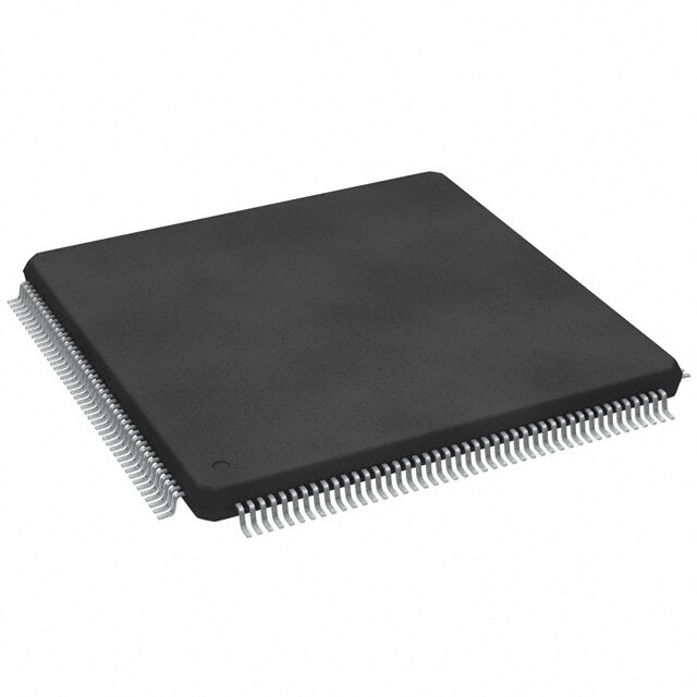
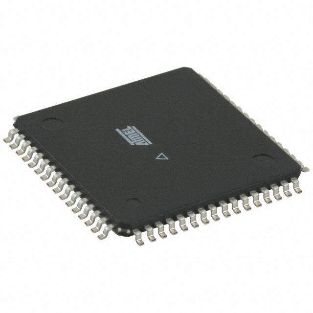
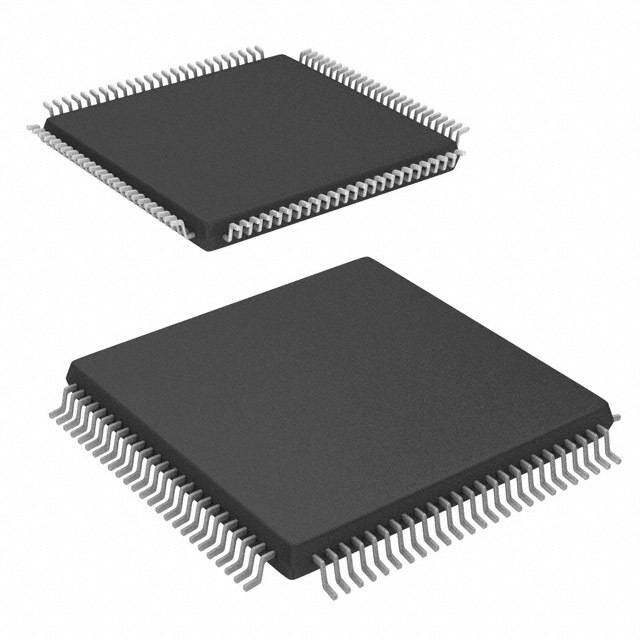
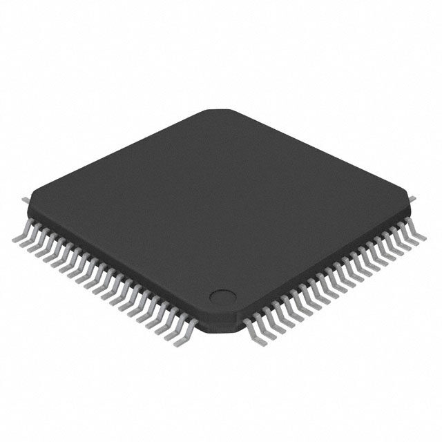
| 产品图片 |
|
| rohs | 符合RoHS无铅 / 符合限制有害物质指令(RoHS)规范要求 |
| 产品系列 | 嵌入式处理器和控制器,微控制器 - MCU,8位微控制器 -MCU,Microchip Technology PIC16F720-I/SOPIC® 16F |
| 数据手册 | http://www.microchip.com/mymicrochip/filehandler.aspx?ddocname=en546269http://www.microchip.com/mymicrochip/filehandler.aspx?ddocname=en552881http://www.microchip.com/mymicrochip/filehandler.aspx?ddocname=en550313http://www.microchip.com/mymicrochip/filehandler.aspx?ddocname=en555608http://www.microchip.com/mymicrochip/filehandler.aspx?ddocname=en545497 |
| 产品型号 | PIC16F720-I/SO |
| PCN设计/规格 | |
| RAM容量 | 128 x 8 |
| 产品培训模块 | http://www.digikey.cn/PTM/IndividualPTM.page?site=cn&lang=zhs&ptm=25053 |
| 产品种类 | 8位微控制器 -MCU |
| 供应商器件封装 | 20-SOIC |
| 其它名称 | PIC16F720ISO |
| 包装 | 管件 |
| 可用A/D通道 | 12 |
| 可编程输入/输出端数量 | 18 |
| 商标 | Microchip Technology |
| 处理器系列 | PIC16 |
| 外设 | 欠压检测/复位,POR,PWM,WDT |
| 安装风格 | SMD/SMT |
| 定时器数量 | 3 Timer |
| 封装 | Tube |
| 封装/外壳 | 20-SOIC(0.295",7.50mm 宽) |
| 封装/箱体 | SOIC-20 |
| 工作温度 | -40°C ~ 85°C |
| 工作电源电压 | 1.8 V to 5.5 V |
| 工厂包装数量 | 38 |
| 振荡器类型 | 内部 |
| 接口类型 | AUSART, I2C, SPI |
| 数据RAM大小 | 128 B |
| 数据Ram类型 | SRAM |
| 数据总线宽度 | 8 bit |
| 数据转换器 | A/D 12x8b |
| 最大工作温度 | + 125 C |
| 最大时钟频率 | 16 MHz |
| 最小工作温度 | - 40 C |
| 标准包装 | 38 |
| 核心 | PIC |
| 核心处理器 | PIC |
| 核心尺寸 | 8-位 |
| 片上ADC | Yes |
| 特色产品 | http://www.digikey.com/cn/zh/ph/Microchip/xlp.html |
| 电压-电源(Vcc/Vdd) | 1.8 V ~ 5.5 V |
| 电源电压-最大 | 5.5 V |
| 电源电压-最小 | 1.8 V |
| 程序存储器大小 | 3.5 kB |
| 程序存储器类型 | FLASH |
| 程序存储容量 | 3.5KB(2K x 14) |
| 系列 | PIC16 |
| 输入/输出端数量 | 18 I/O |
| 连接性 | I²C, SPI, UART/USART |
| 速度 | 16MHz |
-300dpi-lyrd.jpg)


- 商务部:美国ITC正式对集成电路等产品启动337调查
- 曝三星4nm工艺存在良率问题 高通将骁龙8 Gen1或转产台积电
- 太阳诱电将投资9.5亿元在常州建新厂生产MLCC 预计2023年完工
- 英特尔发布欧洲新工厂建设计划 深化IDM 2.0 战略
- 台积电先进制程称霸业界 有大客户加持明年业绩稳了
- 达到5530亿美元!SIA预计今年全球半导体销售额将创下新高
- 英特尔拟将自动驾驶子公司Mobileye上市 估值或超500亿美元
- 三星加码芯片和SET,合并消费电子和移动部门,撤换高东真等 CEO
- 三星电子宣布重大人事变动 还合并消费电子和移动部门
- 海关总署:前11个月进口集成电路产品价值2.52万亿元 增长14.8%


PDF Datasheet 数据手册内容提取
PIC16(L)F720/721 20-Pin Flash Microcontrollers Devices Included In This Data Sheet: Extreme Low-Power (XLP) Features: • PIC16F720 • PIC16LF720 • Sleep Current: - 40 nA @ 1.8V, typical • PIC16F721 • PIC16LF721 • Low-Power Watchdog Timer Current: High-Performance RISC CPU: - 500 nA @ 1.8V, typical • Only 35 Instructions to Learn: Peripheral Features: - All single-cycle instructions except branches • Operating Speed: • Up to 17 I/O Pins and One Input-only Pin: - DC – 16MHz oscillator/clock input - High-current source/sink for direct LED drive - DC – 250ns instruction cycle - Interrupt-on-change pins • Up to 4K x 14 Words of Flash Program Memory - Individually programmable weak pull-ups • Up to 256 bytes of Data Memory (RAM) • A/D Converter: • Interrupt Capability - 8-bit resolution • 8-Level Deep Hardware Stack - 12 channels • Direct, Indirect and Relative Addressing modes - Selectable Voltage reference • Processor Self-Write/Read access to Program • Timer0: 8-Bit Timer/Counter with 8-Bit Memory Programmable Prescaler • Enhanced Timer1 Memory - 16-bit timer/counter with prescaler - External Gate Input mode with toggle and • High-Endurance Flash Data Memory Single Shot modes - 128B of nonvolatile data storage - Interrupt-on-gate completion - 100K erase/write cycles • Timer2: 8-Bit Timer/Counter with 8-Bit Period Register, Prescaler and Postscaler Special Microcontroller Features: • Capture, Compare, PWM module (CCP) - 16-bit Capture, max resolution 12.5ns • Precision Internal Oscillator: - 16-bit Compare, max resolution 250ns - 16 MHz or 500 kHz operation - 10-bit PWM, max frequency 15kHz - Factory calibrated to ±1%, typical • Addressable Universal Synchronous - Software tunable Asynchronous Receiver Transmitter (AUSART) - Software selectable ÷1, ÷2, ÷4 or ÷8 divider • Synchronous Serial Port (SSP) • Power-Saving Sleep mode - SPI (Master/Slave) • Industrial and Extended Temperature Range • Power-on Reset (POR) - I2C (Slave) with Address Mask • Power-up Timer (PWRT) • Brown-out Reset (BOR) • Multiplexed Master Clear with Pull-up/Input Pin • Programmable Code Protection • In-Circuit Serial ProgrammingTM (ICSPTM) via Two Pins • Wide Operating Voltage Range: - 1.8V to 5.5V (PIC16F720/721) - 1.8V to 3.6V (PIC16LF720/721) 2010-2015 Microchip Technology Inc. DS40001430F-page 1
PIC16(L)F720/721 PIC16(L)F72X Family Types h s Device Data Sheet Index Program MemoryFlash (words) Data SRAM(bytes) gh-Endurance FlaMemory (bytes) (2)I/O’s 8-bit ADC (ch) CapSense (ch) Timers(8/16-bit) AUSART 2SSP (IC/SPI) CCP (1)Debug XLP Hi PIC16(L)F707 (1) 8192 363 0 36 14 32 4/2 1 1 2 I Y PIC16(L)F720 (2) 2048 128 128 18 12 — 2/1 1 1 1 I Y PIC16(L)F721 (2) 4096 256 128 18 12 — 2/1 1 1 1 I Y PIC16(L)F722 (4) 2048 128 0 25 11 8 2/1 1 1 2 I Y PIC16(L)F722A (3) 2048 128 0 25 11 8 2/1 1 1 2 I Y PIC16(L)F723 (4) 4096 192 0 25 11 8 2/1 1 1 2 I Y PIC16(L)F723A (3) 4096 192 0 25 11 8 2/1 1 1 2 I Y PIC16(L)F724 (4) 4096 192 0 36 14 16 2/1 1 1 2 I Y PIC16(L)F726 (4) 8192 368 0 25 11 8 2/1 1 1 2 I Y PIC16(L)F727 (4) 8192 368 0 36 14 16 2/1 1 1 2 I Y Note 1: I - Debugging, Integrated on Chip; H - Debugging, Requires Debug Header. 2: One pin is input-only. Data Sheet Index: (Unshaded devices are described in this document.) 1: DS41418 PIC16(L)F707 Data Sheet, 40/44-Pin Flash, 8-bit Microcontrollers 2: DS41430 PIC16(L)F720/721 Data Sheet, 20-Pin Flash, 8-bit Microcontrollers 3: DS41417 PIC16(L)F722A/723A Data Sheet, 28-Pin Flash, 8-bit Microcontrollers 4: DS41341 PIC16(L)F72X Data Sheet, 28/40/44-Pin Flash, 8-bit Microcontrollers Note: For other small form-factor package availability and marking information, please visit http://www.microchip.com/packaging or contact your local sales office. DS40001430F-page 2 2010-2015 Microchip Technology Inc.
PIC16(L)F720/721 PIN DIAGRAMS FIGURE 1: 20-PIN DIAGRAM FOR PIC16(L)F720/721 PDIP, SOIC, SSOP VDD 1 20 VSS RA5/T1CKI/CLKIN 2 19 RA0/AN0/ICSPDAT RA4/AN3/T1G/CLKOUT 3 18 RA1/AN1/ICSPCLK 1 2 RA3/MCLR/VPP 4 7 17 RA2/AN2/T0CKI/INT 0/ RC5/CCP1 5 72 16 RC0/AN4 F RC4 6 L) 15 RC1/AN5 ( 6 RC3/AN7 7 1 14 RC2/AN6 C RC6/AN8/SS 8 PI 13 RB4/AN10/SDI/SDA RC7/AN9/SDO 9 12 RB5/AN11/RX/DT RB7/TX/CK 10 11 RB6/SCK/SCL Pin Diagrams – 20-PIN DIAGRAM FOR PIC16(L)F720/721 QFN (4x4) T U O LK N AT C KI D G/ CL SP 3/T1 CKI/ 0/IC N 1 N A T A RA4/ RA5/ VDD VSS RA0/ 20 19 18 17 16 RA3/MCLR/VPP 1 15 RA1/AN1/ICSPCLK RC5/CCP1 2 14 RA2/AN2/T0CKI/INT PIC16(L)F720/721 RC4 3 13 RC0/AN4 RC3/AN7 4 12 RC1/AN5 RC6/AN8/SS 5 11 RC2/AN6 6 7 8 9 10 O K L T A D C C D D 9/S TX/ K/S RX/ DI/S N 7/ C 1/ S C7/A RB B6/S AN1 N10/ R R 5/ A RB B4/ R 2010-2015 Microchip Technology Inc. DS40001430F-page 3
PIC16(L)F720/721 TABLE 1: 20-PIN ALLOCATION TABLE (PIC16(L)F720/721) C/ OI N I/O Pin PDIP/SSSOP 20-Pin QF A/D Timers CCP AUSART SSP Interrupt Pull-up Basic - 0 2 RA0 19 16 AN0 — — — — IOC Y ICSPDAT RA1 18 15 AN1 — — — — IOC Y ICSPCLK RA2 17 14 AN2 T0CKI — — — INT/IOC — — RA3 4 1 — — — — — IOC Y MCLR/VPP RA4 3 20 AN3 T1G — — — IOC Y CLKOUT RA5 2 19 — T1CKI — — — IOC Y CLKIN RB4 13 10 AN10 — — — SDI/SDA IOC Y — RB5 12 9 AN11 — — RX/DT — IOC Y — RB6 11 8 — — — — SCK/SCL IOC Y — RB7 10 7 — — — TX/CK — IOC Y — RC0 16 13 AN4 — — — — — — — RC1 15 12 AN5 — — — — — — — RC2 14 11 AN6 — — — — — — — RC3 7 4 AN7 — — — — — — — RC4 6 3 — — — — — — — — RC5 5 2 — — CCP1 — — — — — RC6 8 5 AN8 — — — SS — — — RC7 9 6 AN9 — — — SDO — — — VDD 1 18 — — — — — — — VDD Vss 20 17 — — — — — — — VSS DS40001430F-page 4 2010-2015 Microchip Technology Inc.
PIC16(L)F720/721 Table of Contents Device Overview ...................................................................................................................................................................................7 Memory Organization ..........................................................................................................................................................................11 Resets .................................................................................................................................................................................................24 Interrupts............................................................................................................................................................................................. 34 Low Dropout (LDO) Voltage Regulator............................................................................................................................................... 41 I/O Ports ..............................................................................................................................................................................................42 Oscillator Module ................................................................................................................................................................................62 Device Configuration ...........................................................................................................................................................................67 Analog-to-Digital Converter (ADC) Module .........................................................................................................................................71 Fixed Voltage Reference ....................................................................................................................................................................80 Temperature Indicator Module ............................................................................................................................................................82 Timer0 Module ....................................................................................................................................................................................83 Timer1 Module with Gate Control .......................................................................................................................................................86 Timer2 Module ....................................................................................................................................................................................98 Capture/Compare/PWM (CCP) Module ............................................................................................................................................100 Addressable Universal Synchronous Asynchronous Receiver Transmitter (AUSART) ....................................................................109 SSP Module Overview ......................................................................................................................................................................129 Flash Program Memory Self-Read/Self-Write Control ......................................................................................................................151 Power-Down Mode (Sleep) ...............................................................................................................................................................158 In-Circuit Serial Programming™ (ICSP™) ........................................................................................................................................160 Instruction Set Summary ...................................................................................................................................................................161 Development Support .......................................................................................................................................................................170 Electrical Specifications ....................................................................................................................................................................174 DC and AC Characteristics Graphs and Charts ................................................................................................................................200 Packaging Information ......................................................................................................................................................................220 Appendix A: Data Sheet Revision History .........................................................................................................................................230 Appendix B: Migrating From Other PIC® Devices ............................................................................................................................230 The Microchip Website .....................................................................................................................................................................231 Customer Change Notification Service .............................................................................................................................................231 Customer Support .............................................................................................................................................................................231 Product Identification System ...........................................................................................................................................................232 2010-2015 Microchip Technology Inc. DS40001430F-page 5
PIC16(L)F720/721 TO OUR VALUED CUSTOMERS It is our intention to provide our valued customers with the best documentation possible to ensure successful use of your Microchip products. To this end, we will continue to improve our publications to better suit your needs. Our publications will be refined and enhanced as new volumes and updates are introduced. If you have any questions or comments regarding this publication, please contact the Marketing Communications Department via E-mail at docerrors@microchip.com. We welcome your feedback. Most Current Data Sheet To obtain the most up-to-date version of this data sheet, please register at our Worldwide Website at: http://www.microchip.com You can determine the version of a data sheet by examining its literature number found on the bottom outside corner of any page. The last character of the literature number is the version number, (e.g., DS30000000A is version A of document DS30000000). Errata An errata sheet, describing minor operational differences from the data sheet and recommended workarounds, may exist for current devices. As device/documentation issues become known to us, we will publish an errata sheet. The errata will specify the revision of silicon and revision of document to which it applies. To determine if an errata sheet exists for a particular device, please check with one of the following: • Microchip’s Worldwide Website; http://www.microchip.com • Your local Microchip sales office (see last page) When contacting a sales office, please specify which device, revision of silicon and data sheet (include literature number) you are using. Customer Notification System Register on our website at www.microchip.com to receive the most current information on all of our products. DS40001430F-page 6 2010-2015 Microchip Technology Inc.
PIC16(L)F720/721 1.0 DEVICE OVERVIEW The PIC16(L)F720/721 devices are covered by this data sheet. They are available in 20-pin packages. Please refer to Section25.0 “Packaging Information” for further package information. Figure1-1 shows a block diagram of the PIC16(L)F720/721 devices. Table1-1 shows the pinout descriptions. 2010-2015 Microchip Technology Inc. DS40001430F-page 7
PIC16(L)F720/721 FIGURE 1-1: 20-PIN DEVICE BLOCK DIAGRAM FOR PIC16(L)F720/721 CCCooonnnfffiiiggguuurrraaatttiiiooonnn PORTA 111333 DDDaaatttaaa BBBuuusss 888 RA0 PPPrrrooogggrrraaammm CCCooouuunnnttteeerrr RA1 FFFlllaaassshhh RA2 P88rKKo gxxr a11m44 RA3 MPPerrmooggorrraaymm(1) RRRAAAMMM RA4 888 LLLeeevvveeelll SSStttaaaccckkk RA5 MMeemmoorryy FFFiiillleee (((111333---bbbiiittt))) RRReeegggiiisssttteeerrrsss(1) 336688 xx 88 PPPrrrooogggrrraaammm 111444 PPPOOORRRTTTBBB BBBuuusss RRRAAAMMM AAAddddddrrr 999 AAAddddddrrr MMMUUUXXX IIInnnssstttrrruuuccctttiiiooonnn Rrreeeggg RB4 DDDiiirrreeecccttt AAAddddddrrr 777 IIInnndddiiirrreeecccttt RB5 888 AAAddddddrrr RB6 RB7 FFFSSSRRR Rrreeeggg SSSTTTAAATTTUUUSSS Rrreeeggg PPPOOORRRTTTCCC 888 RC0 RRCC11 RC2 333 MMMUUUXXX RC3 Power-up RC4 Timer RC5 IIInnnssstttrrruuuccctttiiiooonnn DDDeeecccooodddeee &&& PPoowweerr--oonn RC6 CCCooonnntttrrrooolll RReesseett AAALLLUUU RC7 CLKIN WWaattcchhddoogg 888 TTiimmeerr CLKOUT GGGeeeTTTnnniiimmmeeerrriiiaaannntttgggiiiooonnn BBrroowwnn--oouutt WWW Rrreeeggg RReesseett LDO Regulator Internal PMDATL Oscillator Self read/ Block write Flash memory MMMCCCLLLRRR VVVDDDDDD VVVSSSSSS PMADRL CCP1 CCP1 ICSPDAT SDI/ SSSCCCKKK/// TX/CKRX/DT ICSPCLK SSSDDDOOOSSSDDDAAA SSSCCCLLL SSSSSS TTT000CCCKKKIII T1G TTT111CCCKKKIII TTTiiimmmeeerrr000 TTTiiimmmeeerrr111 TTTiiimmmeeerrr222 AAUUSSAARRTT AICUSSPA™RT SSSyyynnnccchhhrrrooonnnooouuusss SSSeeerrriiiaaalll PPPooorrrttt Analog-To-Digital Converter AN0 AN1 AN2 AN3 AN4 AN5 AN6 AN7 AN8 AN9 AN10AN11 Note: PIC16(L)F720 – 2k x 14 Flash, 128 x 8 RAM PIC16(L)F721 – 4k x 14 Flash, 256 x 8 RAM. DS40001430F-page 8 2010-2015 Microchip Technology Inc.
PIC16(L)F720/721 TABLE 1-1: PINOUT DESCRIPTION Name Function IN OUT Description RA0/AN0/ICSPDAT General purpose I/O. Individually controlled RA0 TTL CMOS interrupt-on-change. Individually enabled pull-up. AN0 AN — A/D Channel 0 Input. ICSPDAT ST CMOS ICSP™ Data I/O. RA1/AN1/ICSPCLK General purpose I/O. Individually controlled RA1 TTL CMOS interrupt-on-change. Individually enabled pull-up. AN1 AN — A/D Channel 1 Input. ICSPCLK ST — ICSP™ Clock. RA2/AN2/T0CKI/INT RA2 TTL CMOS General purpose I/O with IOC and WPU. AN2 AN — A/D Channel 2 Input. T0CKI ST — Timer0 Clock Input. INT ST — External interrupt. RA3/MCLR/VPP RA3 TTL — General purpose input-only with IOC and WPU. MCLR ST — Master Clear with internal pull-up. VPP HV — Programming Voltage. RA4/AN3/T1G/CLKOUT RA4 TTL CMOS General purpose I/O with IOC and WPU. AN3 AN — A/D Channel 3 Input. T1G ST — Timer1 Gate Input. CLKOUT — CMOS FOSC/4 output. RA5/T1CKI/CLKIN RA5 TTL CMOS General purpose I/O with IOC and WPU. T1CKI ST — Timer1 Clock input. CLKIN ST — External Clock Input (EC mode). RB4/AN10/SDI/SDA RB4 TTL CMOS General purpose I/O with IOC and WPU. AN10 AN — A/D Channel 10 Input. SDI ST — SPI Data Input. SDA I2C OD I2C Data. RB5/AN11/RX/DT RB5 TTL CMOS General purpose I/O with IOC and WPU. AN11 AN — A/D Channel 11 Input. RX ST — USART asynchronous input. DT ST CMOS USART synchronous data. RB6/SCK/SCL RB6 TTL CMOS General purpose I/O with IOC and WPU. SCK ST CMOS SPI Clock. SCL I2C OD I2C Clock. RB7/TX/CK RB7 TTL CMOS General purpose I/O with IOC and WPU. TX — CMOS USART asynchronous transmit. CK ST CMOS USART synchronous clock. RC0/AN4 RC0 ST CMOS General purpose I/O. AN4 AN — A/D Channel 4 Input. RC1/AN5 RC1 ST CMOS General purpose I/O. AN5 AN — A/D Channel 5 Input. RC2/AN6 RC2 ST CMOS General purpose I/O. AN6 AN — A/D Channel 6 Input. RC3/AN7 RC3 ST CMOS General purpose I/O. AN7 AN — A/D Channel 7 Input. Legend: AN = Analog input or output, CMOS = CMOS compatible input or output, OD = Open Drain, TTL = TTL compatible input, ST = Schmitt Trigger input with CMOS levels, I2C = Schmitt Trigger input with I2C, HV = High Voltage, XTAL = Crystal levels 2010-2015 Microchip Technology Inc. DS40001430F-page 9
PIC16(L)F720/721 TABLE 1-1: PINOUT DESCRIPTION (CONTINUED) Name Function IN OUT Description RC4 RC4 ST CMOS General purpose I/O. RC5/CCP1 RC5 ST CMOS General purpose I/O. CCP1 ST CMOS Capture/Compare/PWM 1. RC6/AN8/SS RC6 ST CMOS General purpose I/O. AN8 AN — A/D Channel 8 Input. SS ST — Slave Select input. RC7/AN9/SDO RC7 ST CMOS General purpose I/O. AN9 AN — A/D Channel 9 Input. SDO — CMOS SPI Data Output. VDD VDD Power — Positive supply. Vss Vss Power — Ground supply. Legend: AN = Analog input or output, CMOS = CMOS compatible input or output, OD = Open Drain, TTL = TTL compatible input, ST = Schmitt Trigger input with CMOS levels, I2C = Schmitt Trigger input with I2C, HV = High Voltage, XTAL = Crystal levels DS40001430F-page 10 2010-2015 Microchip Technology Inc.
PIC16(L)F720/721 2.0 MEMORY ORGANIZATION 2.1 Program Memory Organization The PIC16(L)F720/721 has a 13-bit program counter capable of addressing a 8K x14 program memory space. Table2-1 shows the memory sizes implemented. Accessing a location above these boundaries will cause a wrap-around within the implemented memory space. The Reset vector is at 0000h and the interrupt vector is at 0004h. TABLE 2-1: DEVICE SIZE AND ADDRESSES Program Memory Size Last Program Memory High-Endurance Flash Device (Words) Address Memory Address Range (1) PIC16F720 2048 07FFh 0780h-07FFh PIC16LF720 PIC16F721 4096 0FFFh 0F80h-0FFFh PIC16LF721 Note 1: High-Endurance Flash applies to the low byte of each address in the range. FIGURE 2-1: PROGRAM MEMORY MAP FIGURE 2-2: PROGRAM MEMORY MAP AND STACK FOR THE AND STACK FOR THE PIC16(L)F720 PIC16(L)F721 PC<12:0> PC<12:0> CALL, RETURN 13 CALL, RETURN 13 RETFIE, RETLW RETFIE, RETLW Stack Level 1 Stack Level 1 Stack Level 2 Stack Level 2 Stack Level 8 Stack Level 8 Reset Vector 0000h Reset Vector 0000h Interrupt Vector 0004H Interrupt Vector 0004H On-chip 0005h 0005h Program Page 0 Page 0 On-chip Memory 07FFh 07FFh Program 0800h Memory 0800h Wraps to Page 0 Page 1 0FFFh 0FFFh 1000h 1000h Wraps to Page 0 Wraps to Page 0 17FFh 17FFh 1800h 1800h Wraps to Page 1 Wraps to Page 0 1FFFh 1FFFh 2010-2015 Microchip Technology Inc. DS40001430F-page 11
PIC16(L)F720/721 2.2 Data Memory Organization The data memory is partitioned into multiple banks which contain the General Purpose Registers (GPRs) and the Special Function Registers (SFRs). Bits RP0 and RP1 are bank select bits. RP1 RP0 0 0 Bank 0 is selected 0 1 Bank 1 is selected 1 0 Bank 2 is selected 1 1 Bank 3 is selected Each bank extends up to 7Fh (128 bytes). The lower locations of each bank are reserved for the Special Function Registers. Above the Special Function Registers are the General Purpose Registers, implemented as static RAM. All implemented banks contain Special Function Registers. Some frequently used Special Function Registers from one bank are mirrored in another bank for code reduction and quicker access. 2.2.1 GENERAL PURPOSE REGISTER FILE The register file is organized as 128x8 bits in the PIC16(L)F720, 256x8 bits in the PIC16(L)F721. Each register is accessed either directly or indirectly through the File Select Register (FSR), (Refer to Section2.5 “Indirect Addressing, INDF and FSR Registers”). 2.2.2 SPECIAL FUNCTION REGISTERS The Special Function Registers are registers used by the CPU and peripheral functions for controlling the desired operation of the device (refer to Table2-2). These registers are static RAM. The Special Function Registers can be classified into two sets: core and peripheral. The Special Function Registers associated with the “core” are described in this section. Those related to the operation of the peripheral features are described in the section of that peripheral feature. DS40001430F-page 12 2010-2015 Microchip Technology Inc.
PIC16(L)F720/721 FIGURE 2-3: PIC16(L)F720 SPECIAL FUNCTION REGISTERS File Address INDF(*) 00h INDF(*) 80h INDF(*) 100h INDF(*) 180h TMR0 01h OPTION_REG 81h TMR0 101h OPTION_REG 181h PCL 02h PCL 82h PCL 102h PCL 182h STATUS 03h STATUS 83h STATUS 103h STATUS 183h FSR 04h FSR 84h FSR 104h FSR 184h PORTA 05h TRISA 85h 105h ANSELA 185h PORTB 06h TRISB 86h 106h ANSELB 186h PORTC 07h TRISC 87h 107h ANSELC 187h 08h 88h 108h 188h 09h 89h 109h 189h PCLATH 0Ah PCLATH 8Ah PCLATH 10Ah PCLATH 18Ah INTCON 0Bh INTCON 8Bh INTCON 10Bh INTCON 18Bh PIR1 0Ch PIE1 8Ch PMDATL 10Ch PMCON1 18Ch 0Dh 8Dh PMADRL 10Dh PMCON2 18Dh TMR1L 0Eh PCON 8Eh PMDATH 10Eh 18Eh TMR1H 0Fh T1GCON 8Fh PMADRH 10Fh 18Fh T1CON 10h OSCCON 90h 110h 190h TMR2 11h OSCTUNE 91h 111h 191h T2CON 12h PR2 92h 112h 192h SSPBUF 13h SSPADD/SSPMSK93h 113h 193h SSPCON 14h SSPSTAT 94h 114h 194h CCPR1L 15h WPUA 95h WPUB 115h 195h CCPR1H 16h IOCA 96h IOCB 116h 196h CCP1CON 17h 97h 117h 197h RCSTA 18h TXSTA 98h 118h 198h TXREG 19h SPBRG 99h 119h 199h RCREG 1Ah 9Ah 11Ah 19Ah 1Bh 9Bh 11Bh 19Bh 1Ch 9Ch 11Ch 19Ch 1Dh FVRCON 9Dh 11Dh 19Dh ADRES 1Eh 9Eh 11Eh 19Eh ADCON0 1Fh ADCON1 9Fh 11Fh 19Fh 20h A0h 120h 1A0h General General Purpose Purpose Register Register 32 Bytes 80 Bytes BFh C0h 06Fh EFh 16Fh 1EFh 070h F0h 170h 1F0h Accesses Accesses Accesses Access RAM 70h – 7Fh 70h – 7Fh 70h – 7Fh 7Fh FFh 17Fh 1FFh BANK 0 BANK 1 BANK 2 BANK 3 Legend: = Unimplemented data memory locations, read as ‘0’. * = Not a physical register. 2010-2015 Microchip Technology Inc. DS40001430F-page 13
PIC16(L)F720/721 FIGURE 2-4: PIC16(L)F721 SPECIAL FUNCTION REGISTERS File Address INDF(*) 00h INDF(*) 80h INDF(*) 100h INDF(*) 180h TMR0 01h OPTION_REG 81h TMR0 101h OPTION_REG 181h PCL 02h PCL 82h PCL 102h PCL 182h STATUS 03h STATUS 83h STATUS 103h STATUS 183h FSR 04h FSR 84h FSR 104h FSR 184h PORTA 05h TRISA 85h 105h ANSELA 185h PORTB 06h TRISB 86h 106h ANSELB 186h PORTC 07h TRISC 87h 107h ANSELC 187h 08h 88h 108h 188h 09h 89h 109h 189h PCLATH 0Ah PCLATH 8Ah PCLATH 10Ah PCLATH 18Ah INTCON 0Bh INTCON 8Bh INTCON 10Bh INTCON 18Bh PIR1 0Ch PIE1 8Ch PMDATL 10Ch PMCON1 18Ch 0Dh 8Dh PMADRL 10Dh PMCON2 18Dh TMR1L 0Eh PCON 8Eh PMDATH 10Eh 18Eh TMR1H 0Fh T1GCON 8Fh PMADRH 10Fh 18Fh T1CON 10h OSCCON 90h 110h 190h TMR2 11h OSCTUNE 91h 111h 191h T2CON 12h PR2 92h 112h 192h SSPBUF 13h SSPADD/SSPMSK93h 113h 193h SSPCON 14h SSPSTAT 94h 114h 194h CCPR1L 15h WPUA 95h WPUB 115h 195h CCPR1H 16h IOCA 96h IOCB 116h 196h CCP1CON 17h 97h 117h 197h RCSTA 18h TXSTA 98h 118h 198h TXREG 19h SPBRG 99h 119h 199h RCREG 1Ah 9Ah 11Ah 19Ah 1Bh 9Bh 11Bh 19Bh 1Ch 9Ch 11Ch 19Ch 1Dh FVRCON 9Dh 11Dh 19Dh ADRES 1Eh 9Eh 11Eh 19Eh ADCON0 1Fh ADCON1 9Fh 11Fh 19Fh 20h A0h 120h 1A0h General General General Purpose Purpose Purpose Register Register Register 80 Bytes 80 Bytes 80 Bytes 06Fh EFh 16Fh 1EFh 070h Accesses F0h Accesses 170h Accesses 1F0h Access RAM 70h – 7Fh 70h – 7Fh 70h – 7Fh 7Fh FFh 17Fh 1FFh BANK 0 BANK 1 BANK 2 BANK 3 Legend: = Unimplemented data memory locations, read as ‘0’. * = Not a physical register. DS40001430F-page 14 2010-2015 Microchip Technology Inc.
PIC16(L)F720/721 TABLE 2-2: SPECIAL FUNCTION REGISTER SUMMARY Value on all Value on Address Name Bit 7 Bit 6 Bit 5 Bit 4 Bit 3 Bit 2 Bit 1 Bit 0 other POR, BOR Resets Bank 0 00h(2) INDF Addressing this location uses contents of FSR to address data memory (not a physical register) xxxx xxxx xxxx xxxx 01h TMR0 Timer0 module Register xxxx xxxx uuuu uuuu 02h(2) PCL Program Counter (PC) Least Significant Byte 0000 0000 0000 0000 03h(2) STATUS IRP RP1 RP0 TO PD Z DC C 0001 1xxx 000q quuu 04h(2) FSR Indirect Data Memory Address Pointer xxxx xxxx uuuu uuuu 05h PORTA — — RA5 RA4 RA3 RA2 RA1 RA0 --xx xxxx --xx xxxx 06h PORTB RB7 RB6 RB5 RB4 — — — — xxxx ---- uuuu ---- 07h PORTC RC7 RC6 RC5 RC4 RC3 RC2 RC1 RC0 xxxx xxxx uuuu uuuu 08h — Unimplemented — — 09h — Unimplemented — — 0Ah(1),(2) PCLATH — — — Write Buffer for the upper 5 bits of the Program Counter ---0 0000 ---0 0000 0Bh(2) INTCON GIE PEIE TMR0IE INTE RABIE TMR0IF INTF RABIF 0000 000x 0000 000x 0Ch PIR1 TMR1GIF ADIF RCIF TXIF SSPIF CCP1IF TMR2IF TMR1IF 0000 0000 0000 0000 0Dh — Unimplemented — — 0Eh TMR1L Holding Register for the Least Significant Byte of the 16-bit TMR1 Register xxxx xxxx uuuu uuuu 0Fh TMR1H Holding Register for the Most Significant Byte of the 16-bit TMR1 Register xxxx xxxx uuuu uuuu 10h T1CON TMR1CS1 TMR1CS0 T1CKPS1 T1CKPS0 — T1SYNC — TMR1ON 0000 -0-0 uuuu -u-u 11h TMR2 Timer2 module Register 0000 0000 0000 0000 12h T2CON — TOUTPS3 TOUTPS2 TOUTPS1 TOUTPS0 TMR2ON T2CKPS1 T2CKPS0 -000 0000 -000 0000 13h SSPBUF Synchronous Serial Port Receive Buffer/Transmit Register xxxx xxxx uuuu uuuu 14h SSPCON WCOL SSPOV SSPEN CKP SSPM3 SSPM2 SSPM1 SSPM0 0000 0000 0000 0000 15h CCPR1L Capture/Compare/PWM Register Low Byte xxxx xxxx uuuu uuuu 16h CCPR1H Capture/Compare/PWM Register High Byte xxxx xxxx uuuu uuuu 17h CCP1CON — — DC1 B1 CCP1M3 CCP1M2 CCP1M1 CCP1M0 --00 0000 --00 0000 18h RCSTA SPEN RX9 SREN CREN ADDEN FERR OERR RX9D 0000 000x 0000 000x 19h TXREG AUSART Transmit Data Register 0000 0000 0000 0000 1Ah RCREG AUSART Receive Data Register 0000 0000 0000 0000 1Bh — Unimplemented — — 1Ch — Unimplemented — — 1Dh — Unimplemented — — 1Eh ADRES ADC Result Register xxxx xxxx uuuu uuuu 1Fh ADCON0 — — CHS3 CHS2 CHS1 CHS0 GO/ ADON --00 0000 --00 0000 DONE Legend: x = unknown, u = unchanged, q = value depends on condition, - = unimplemented, read as ‘0’, r = reserved. Shaded locations are unimplemented, read as ‘0’. Note 1: The upper byte of the program counter is not directly accessible. PCLATH is a holding register for the PC<12:8>, whose contents are transferred to the upper byte of the program counter. 2: These registers can be addressed from any bank. 3: Accessible only when SSPM<3:0> = 1001. 4: This bit is unimplemented and reads as ‘1’. 5: See Register6-2. 2010-2015 Microchip Technology Inc. DS40001430F-page 15
PIC16(L)F720/721 TABLE 2-2: SPECIAL FUNCTION REGISTER SUMMARY (CONTINUED) Value on all Value on Address Name Bit 7 Bit 6 Bit 5 Bit 4 Bit 3 Bit 2 Bit 1 Bit 0 other POR, BOR Resets Bank 1 80h(2) INDF Addressing this location uses contents of FSR to address data memory (not a physical register) xxxx xxxx xxxx xxxx 81h OPTION_ RABPU INTEDG T0CS T0SE PSA PS2 PS1 PS0 1111 1111 1111 1111 REG 82h(2) PCL Program Counter (PC) Least Significant Byte 0000 0000 0000 0000 83h(2) STATUS IRP RP1 RP0 TO PD Z DC C 0001 1xxx 000q quuu 84h(2) FSR Indirect Data Memory Address Pointer xxxx xxxx uuuu uuuu 85h(5) TRISA — — TRISA5 TRISA4 —(4) TRISA2 TRISA1 TRISA0 --11 -111 --11 -111 86h TRISB TRISB7 TRISB6 TRISB5 TRISB4 — — — — 1111 ---- 1111 ---- 87h TRISC TRISC7 TRISC6 TRISC5 TRISC4 TRISC3 TRISC2 TRISC1 TRISC0 1111 1111 1111 1111 88h — Unimplemented — — 89h — Unimplemented — — 8Ah(1),(2) PCLATH — — — Write Buffer for the upper 5 bits of the Program Counter ---0 0000 ---0 0000 8Bh(2) INTCON GIE PEIE TMR0IE INTE RABIE TMR0IF INTF RABIF 0000 000x 0000 000x 8Ch PIE1 TMR1GIE ADIE RCIE TXIE SSPIE CCP1IE TMR2IE TMR1IE 0000 0000 0000 0000 8Dh — Unimplemented — — 8Eh PCON — — — — — — POR BOR ---- --qq ---- --uu 8Fh T1GCON TMR1GE T1GPOL T1GTM T1GSPM T1GGO/ T1GVAL T1GSS1 T1GSS0 0000 0x00 uuuu uxuu DONE 90h OSCCON — — IRCF1 IRCF0 ICSL ICSS — — --10 qq-- --10 qq-- 91h OSCTUNE — — TUN5 TUN4 TUN3 TUN2 TUN1 TUN0 --00 0000 --uu uuuu 92h PR2 Timer2 module Period Register 1111 1111 1111 1111 93h SSPADD ADD<7:0> 0000 0000 0000 0000 93h(3) SSPMSK MSK<7:0> 1111 1111 1111 1111 94h SSPSTAT SMP CKE D/A P S R/W UA BF 0000 0000 0000 0000 95h WPUA — — WPUA5 WPUA4 WPUA3 WPUA2 WPUA1 WPUA0 --11 1111 --11 1111 96h IOCA — — IOCA5 IOCA4 IOCA3 IOCA2 IOCA1 IOCA0 --00 0000 --00 0000 97h — Unimplemented — — 98h TXSTA CSRC TX9 TXEN SYNC — BRGH TRMT TX9D 0000 -010 0000 -010 99h SPBRG BRG7 BRG6 BRG5 BRG4 BRG3 BRG2 BRG1 BRG0 0000 0000 0000 0000 9Ah — Unimplemented — — 9Bh — Unimplemented — — 9Ch — Unimplemented — — 9Dh FVRCON FVRRDY FVREN TSEN TSRNG — — ADFVR1 ADFVR0 q000 --00 q000 --00 9Eh — Unimplemented — — 9Fh ADCON1 — ADCS2 ADCS1 ADCS0 — — — — -000 ---- -000 ---- Legend: x = unknown, u = unchanged, q = value depends on condition, - = unimplemented, read as ‘0’, r = reserved. Shaded locations are unimplemented, read as ‘0’. Note 1: The upper byte of the program counter is not directly accessible. PCLATH is a holding register for the PC<12:8>, whose contents are transferred to the upper byte of the program counter. 2: These registers can be addressed from any bank. 3: Accessible only when SSPM<3:0> = 1001. 4: This bit is unimplemented and reads as ‘1’. 5: See Register6-2. DS40001430F-page 16 2010-2015 Microchip Technology Inc.
PIC16(L)F720/721 TABLE 2-2: SPECIAL FUNCTION REGISTER SUMMARY (CONTINUED) Value on all Value on Address Name Bit 7 Bit 6 Bit 5 Bit 4 Bit 3 Bit 2 Bit 1 Bit 0 other POR, BOR Resets Bank 2 100h(2) INDF Addressing this location uses contents of FSR to address data memory (not a physical register) xxxx xxxx xxxx xxxx 101h TMR0 Timer0 module Register xxxx xxxx uuuu uuuu 102h(2) PCL Program Counter (PC) Least Significant Byte 0000 0000 0000 0000 103h(2) STATUS IRP RP1 RP0 TO PD Z DC C 0001 1xxx 000q quuu 104h(2) FSR Indirect Data Memory Address Pointer xxxx xxxx uuuu uuuu 105h — Unimplemented — — 106h — Unimplemented — — 107h — Unimplemented — — 108h — Unimplemented — — 109h — Unimplemented — — 10Ah(1),(2) PCLATH — — — Write Buffer for the upper 5 bits of the Program Counter ---0 0000 ---0 0000 10Bh(2) INTCON GIE PEIE TMR0IE INTE RABIE TMR0IF INTF RABIF 0000 000x 0000 000x 10Ch PMDATL Program Memory Read Data Register Low Byte xxxx xxxx xxxx xxxx 10Dh PMADRL Program Memory Read Address Register Low Byte 0000 0000 0000 0000 10Eh PMDATH — — Program Memory Read Data Register High Byte --xx xxxx --xx xxxx 10Fh PMADRH — — — Program Memory Read Address Register High Byte ---0 0000 ---0 0000 110h — Unimplemented — — 111h — Unimplemented — — 112h — Unimplemented — — 113h — Unimplemented — — 114h — Unimplemented — — 115h WPUB WPUB7 WPUB6 WPUB5 WPUB4 — — — — 1111 ---- 1111 ---- 116h IOCB IOCB7 IOCB6 IOCB5 IOCB4 — — — — 0000 ---- 0000 ---- 117h — Unimplemented — — 118h — Unimplemented — — 119h — Unimplemented — — 11Ah — Unimplemented — — 11Bh — Unimplemented — — 11Ch — Unimplemented — — 11Dh — Unimplemented — — 11Eh — Unimplemented — — 11Fh — Unimplemented — — Legend: x = unknown, u = unchanged, q = value depends on condition, - = unimplemented, read as ‘0’, r = reserved. Shaded locations are unimplemented, read as ‘0’. Note 1: The upper byte of the program counter is not directly accessible. PCLATH is a holding register for the PC<12:8>, whose contents are transferred to the upper byte of the program counter. 2: These registers can be addressed from any bank. 3: Accessible only when SSPM<3:0> = 1001. 4: This bit is unimplemented and reads as ‘1’. 5: See Register6-2. 2010-2015 Microchip Technology Inc. DS40001430F-page 17
PIC16(L)F720/721 TABLE 2-2: SPECIAL FUNCTION REGISTER SUMMARY (CONTINUED) Value on all Value on Address Name Bit 7 Bit 6 Bit 5 Bit 4 Bit 3 Bit 2 Bit 1 Bit 0 other POR, BOR Resets Bank 3 180h(2) INDF Addressing this location uses contents of FSR to address data memory (not a physical register) xxxx xxxx xxxx xxxx 181h OPTION_ RABPU INTEDG T0CS T0SE PSA PS2 PS1 PS0 1111 1111 1111 1111 REG 182h(2) PCL Program Counter (PC) Least Significant Byte 0000 0000 0000 0000 183h(2) STATUS IRP RP1 RP0 TO PD Z DC C 0001 1xxx 000q quuu 184h(2) FSR Indirect Data Memory Address Pointer xxxx xxxx uuuu uuuu 185h ANSELA — — — ANSA4 — ANSA2 ANSA1 ANSA0 ---1 -111 ---1 -111 186h ANSELB — — ANSB5 ANSB4 — — — — --11 ---- --11 ---- 187h ANSELC ANSC7 ANSC6 — — ANSC3 ANSC2 ANSC1 ANSC0 11-- 1111 11-- 1111 188h — Unimplemented — — 18Ah(1),(2) PCLATH — — — Write Buffer for the upper 5 bits of the Program Counter ---0 0000 ---0 0000 18Bh(2) INTCON GIE PEIE TMR0IE INTE RABIE TMR0IF INTF RABIF 0000 000x 0000 000x 18Ch PMCON1 —(4) CFGS LWLO FREE — WREN WR RD 1000 -000 1000 -000 18Dh PMCON2 Program Memory Control Register 2 (not a physical register) ---- ---- ---- ---- 190h — Unimplemented — — 191h — Unimplemented — — 192h — Unimplemented — — 193h — Unimplemented — — 194h — Unimplemented — — 195h — Unimplemented — — 196h — Unimplemented — — 197h — Unimplemented — — 198h — Unimplemented — — 199h — Unimplemented — — 19Ah — Unimplemented — — 19Bh — Unimplemented — — 19Ch — Unimplemented — — 19Dh — Unimplemented — — 19Eh — Unimplemented — — 19Fh — Unimplemented — — Legend: x = unknown, u = unchanged, q = value depends on condition, - = unimplemented, read as ‘0’, r = reserved. Shaded locations are unimplemented, read as ‘0’. Note 1: The upper byte of the program counter is not directly accessible. PCLATH is a holding register for the PC<12:8>, whose contents are transferred to the upper byte of the program counter. 2: These registers can be addressed from any bank. 3: Accessible only when SSPM<3:0> = 1001. 4: This bit is unimplemented and reads as ‘1’. 5: See Register6-2. DS40001430F-page 18 2010-2015 Microchip Technology Inc.
PIC16(L)F720/721 2.2.2.1 STATUS Register For example, CLRF STATUS will clear the upper three bits and set the Z bit. This leaves the STATUS register The STATUS register, shown in Register2-1, contains: as ‘000u u1uu’ (where u = unchanged). • the arithmetic status of the ALU It is recommended, therefore, that only BCF, BSF, • the Reset status SWAPF and MOVWF instructions are used to alter the • the bank select bits for data memory (SRAM) STATUS register, because these instructions do not The STATUS register can be the destination for any affect any Status bits. For other instructions not instruction, like any other register. If the STATUS affecting any Status bits (Refer to Section21.0 register is the destination for an instruction that affects “Instruction Set Summary”). the Z, DC or C bits, then the write to these three bits is Note1: The C and DC bits operate as Borrow disabled. These bits are set or cleared according to the and Digit Borrow out bits, respectively, in device logic. Furthermore, the TO and PD bits are not subtraction. writable. Therefore, the result of an instruction with the STATUS register as destination may be different than intended. REGISTER 2-1: STATUS: STATUS REGISTER R/W-0 R/W-0 R/W-0 R-1 R-1 R/W-x R/W-x R/W-x IRP RP1 RP0 TO PD Z DC(1) C(1) bit 7 bit 0 Legend: R = Readable bit W = Writable bit U = Unimplemented bit, read as ‘0’ -n = Value at POR ‘1’ = Bit is set ‘0’ = Bit is cleared x = Bit is unknown bit 7 IRP: Register Bank Select bit (used for indirect addressing) 1 = Bank 2, 3 (100h-1FFh) 0 = Bank 0, 1 (00h-FFh) bit 6-5 RP<1:0>: Register Bank Select bits (used for direct addressing) 00 = Bank 0 (00h-7Fh) 01 = Bank 1 (80h-FFh) 10 = Bank 2 (100h-17Fh) 11 = Bank 3 (180h-1FFh) bit 4 TO: Time-out bit 1 = After power-up, CLRWDT instruction or SLEEP instruction 0 = A WDT time out occurred bit 3 PD: Power-down bit 1 = After power-up or by the CLRWDT instruction 0 = By execution of the SLEEP instruction bit 2 Z: Zero bit 1 = The result of an arithmetic or logic operation is zero 0 = The result of an arithmetic or logic operation is not zero bit 1 DC: Digit Carry/Digit Borrow bit (ADDWF, ADDLW,SUBLW,SUBWF instructions)(1) 1 = A carry out from the 4th low-order bit of the result occurred 0 = No carry out from the 4th low-order bit of the result bit 0 C: Carry/Borrow bit(1) (ADDWF, ADDLW, SUBLW, SUBWF instructions)(1) 1 = A carry out from the Most Significant bit of the result occurred 0 = No carry out from the Most Significant bit of the result occurred Note 1: For Borrow, the polarity is reversed. A subtraction is executed by adding the two’s complement of the second operand. For rotate instructions (RRF, RLF), this bit is loaded with either the high-order or low-order bit of the source register. 2010-2015 Microchip Technology Inc. DS40001430F-page 19
PIC16(L)F720/721 2.2.2.2 OPTION_REG Register Note: To achieve a 1:1 prescaler assignment for The OPTION_REG register, shown in Register2-2, is Timer0, assign the prescaler to the WDT a readable and writable register, which contains by setting the PSA bit of the various control bits to configure: OPTION_REG register to ‘1’. Refer to • Software programmable prescaler for the Timer0/ Section12.1.3 “Software WDT Programmable Prescaler”. • External RA2/INT interrupt • Timer0 • Weak pull-ups on PORTA or PORTB REGISTER 2-2: OPTION_REG: OPTION REGISTER R/W-1 R/W-1 R/W-1 R/W-1 R/W-1 R/W-1 R/W-1 R/W-1 RABPU INTEDG T0CS T0SE PSA PS2 PS1 PS0 bit 7 bit 0 Legend: R = Readable bit W = Writable bit U = Unimplemented bit, read as ‘0’ -n = Value at POR ‘1’ = Bit is set ‘0’ = Bit is cleared x = Bit is unknown bit 7 RABPU: PORTA or PORTB Pull-up Enable bit 1 = PORTA or PORTB pull-ups are disabled 0 = PORTA or PORTB pull-ups are enabled by individual bits in the WPUA or WPUB register, respectively bit 6 INTEDG: Interrupt Edge Select bit 1 = Interrupt on rising edge of INT pin 0 = Interrupt on falling edge of INT pin bit 5 T0CS: Timer0 Clock Source Select bit 1 = Transition on T0CKI pin 0 = Internal instruction cycle clock (FOSC/4) bit 4 T0SE: Timer0 Source Edge Select bit 1 = Increment on high-to-low transition on T0CKI pin 0 = Increment on low-to-high transition on T0CKI pin bit 3 PSA: Prescaler Assignment bit 1 = Prescaler is assigned to the WDT 0 = Prescaler is assigned to the Timer0 module bit 2-0 PS<2:0>: Prescaler Rate Select bits Bit Value Timer0 Rate WDT Rate 000 1 : 2 1 : 1 001 1 : 4 1 : 2 010 1 : 8 1 : 4 011 1 : 16 1 : 8 100 1 : 32 1 : 16 101 1 : 64 1 : 32 110 1 : 128 1 : 64 111 1 : 256 1 : 128 DS40001430F-page 20 2010-2015 Microchip Technology Inc.
PIC16(L)F720/721 2.2.2.3 PCON Register The Power Control (PCON) register contains flag bits (refer to Table3-4) to differentiate between a: • Power-on Reset (POR) • Brown-out Reset (BOR) • Watchdog Timer Reset (WDT) • External MCLR Reset The PCON register also controls the software enable of the BOR. The PCON register bits are shown in Register2-3. REGISTER 2-3: PCON: POWER CONTROL REGISTER U-0 U-0 U-0 U-0 U-0 U-0 R/W-q R/W-q — — — — — — POR BOR bit 7 bit 0 Legend: R = Readable bit W = Writable bit U = Unimplemented bit, read as ‘0’ -n = Value at POR ‘1’ = Bit is set ‘0’ = Bit is cleared x = Bit is unknown q = Value depends on condition bit 7-2 Unimplemented: Read as ‘0’ bit 1 POR: Power-on Reset Status bit 1 = No Power-on Reset occurred 0 = A Power-on Reset occurred (must be set in software after a Power-on Reset occurs) bit 0 BOR: Brown-out Reset Status bit 1 = No Brown-out Reset occurred 0 = A Brown-out Reset occurred (must be set in software after a Power-on Reset or Brown-out Reset occurs) 2010-2015 Microchip Technology Inc. DS40001430F-page 21
PIC16(L)F720/721 2.3 PCL and PCLATH Note1: There are no Status bits to indicate stack The Program Counter (PC) is 13 bits wide. The low overflow or stack underflow conditions. byte comes from the PCL register, which is a readable and writable register. The high byte (PC<12:8>) is not 2: There are no instructions/mnemonics directly readable or writable and comes from called PUSH or POP. These are actions PCLATH. On any Reset, the PC is cleared. Figure2-5 that occur from the execution of the shows the two situations for the loading of the PC. The CALL, RETURN, RETLW and RETFIE upper example in Figure2-5 shows how the PC is instructions or the vectoring to an loaded on a write to PCL (PCLATH<4:0> PCH). interrupt address. The lower example in Figure2-5 shows how the PC is loaded during a CALL or GOTO instruction 2.4 Program Memory Paging (PCLATH<4:3> PCH). All devices are capable of addressing a continuous 8K FIGURE 2-5: LOADING OF PC IN word block of program memory. The CALL and GOTO instructions provide only 11 bits of address to allow DIFFERENT SITUATIONS branching within any 2K program memory page. When PCH PCL doing a CALL or GOTO instruction, the upper two bits of Instruction with 12 8 7 0 PCL as the address are provided by PCLATH<4:3>. When PC Destination doing a CALL or GOTO instruction, the user must ensure that the page Select bits are programmed so that the PCLATH<4:0> 8 5 ALU Result desired program memory page is addressed. If a return from a CALL instruction (or interrupt) is executed, the entire 13-bit PC is POPed off the stack. Therefore, PCLATH manipulation of the PCLATH<4:3> bits is not required PCH PCL for the RETURN instructions (which POPs the address 12 11 10 8 7 0 from the stack). PC GOTO, CALL Note: The contents of the PCLATH register are PCLATH<4:3> 11 unchanged after a RETURN or RETFIE 2 Opcode<10:0> instruction is executed. The user must rewrite the contents of the PCLATH PCLATH register for any subsequent subroutine calls or GOTO instructions. 2.3.1 COMPUTED GOTO Example2-1 shows the calling of a subroutine in page A computed GOTO is accomplished by adding an offset 1 of the program memory. This example assumes that to the program counter (ADDWF PCL). When perform- PCLATH is saved and restored by the Interrupt Service ing a table read using a computed GOTO method, care Routine (if interrupts are used). should be exercised if the table location crosses a PCL memory boundary (each 256-byte block). Refer to the EXAMPLE 2-1: CALL OF A SUBROUTINE Application Note AN556, “Implementing a Table Read” IN PAGE 1 FROM PAGE 0 (DS00556). ORG 500h PAGESELSUB_P1 ;Select page 1 2.3.2 STACK ;(800h-FFFh) All devices have an 8-levelx13-bit wide hardware CALL SUB1_P1;Call subroutine in stack (refer to Figures2-1 and2-2). The stack space is : ;page 1 (800h-FFFh) not part of either program or data space and the Stack : Pointer is not readable or writable. The PC is PUSHed ORG 900h ;page 1 (800h-FFFh) SUB1_P1 onto the stack when a CALL instruction is executed or : ;called subroutine an interrupt causes a branch. The stack is POPed in ;page 1 (800h-FFFh) the event of a RETURN, RETLW or a RETFIE instruction : execution. PCLATH is not affected by a PUSH or POP RETURN ;return to operation. ;Call subroutine The stack operates as a circular buffer. This means that ;in page 0 ;(000h-7FFh) after the stack has been PUSHed eight times, the ninth PUSH overwrites the value that was stored from the first PUSH. The tenth PUSH overwrites the second PUSH (and so on). DS40001430F-page 22 2010-2015 Microchip Technology Inc.
PIC16(L)F720/721 2.5 Indirect Addressing, INDF and EXAMPLE 2-2: INDIRECT ADDRESSING FSR Registers MOVLW 020h ;initialize pointer MOVWF FSR ;to RAM The INDF register is not a physical register. Addressing BANKISEL 020h the INDF register will cause indirect addressing. NEXT CLRF INDF ;clear INDF register Indirect addressing is possible by using the INDF INCF FSR ;inc pointer BTFSS FSR,4 ;all done? register. Any instruction using the INDF register GOTO NEXT ;no clear next actually accesses data pointed to by the File Select CONTINUE ;yes continue Register (FSR). Reading INDF itself indirectly will produce 00h. Writing to the INDF register indirectly results in a no operation (although Status bits may be affected). An effective 9-bit address is obtained by concatenating the 8-bit FSR register and the IRP bit of the STATUS register, as shown in Figure2-6. A simple program to clear the RAM location 020h-02Fh using indirect addressing is shown in Example2-2. FIGURE 2-6: DIRECT/INDIRECT ADDRESSING Direct Addressing Indirect Addressing RP1 RP0 6 From Opcode 0 IRP 7 File Select Register0 Bank Select Location Select Bank Select Location Select 00 01 10 11 00h 180h Data Memory 7Fh 1FFh Bank 0 Bank 1 Bank 2 Bank 3 Note: For memory map detail, refer to Figures2-3 and 2-4. 2010-2015 Microchip Technology Inc. DS40001430F-page 23
PIC16(L)F720/721 3.0 RESETS Most registers are not affected by a WDT wake-up since this is viewed as the resumption of normal The PIC16(L)F720/721 differentiates between various operation. TO and PD bits are set or cleared differently kinds of Reset: in different Reset situations, as indicated in Table3-5. a) Power-on Reset (POR) These bits are used in software to determine the nature of the Reset. b) WDT Reset during normal operation c) WDT Reset during Sleep A simplified block diagram of the On-Chip Reset Circuit is shown in Figure3-1. d) MCLR Reset during normal operation e) MCLR Reset during Sleep The MCLR Reset path has a noise filter to detect and ignore small pulses. See Section23.0 “Electrical f) Brown-out Reset (BOR) Specifications” for pulse-width specifications. Some registers are not affected in any Reset condition; their status is unknown on POR and unchanged in any other Reset. Most other registers are reset to a “Reset state” on: • Power-on Reset (POR) • MCLR Reset • MCLR Reset during Sleep • WDT Reset • Brown-out Reset (BOR) FIGURE 3-1: SIMPLIFIED BLOCK DIAGRAM OF ON-CHIP RESET CIRCUIT MCLRE MCLR/VPP Sleep WDT WDT Module Time-out Reset POR Power-on Reset VDD Brown-out(1) Reset BOREN Chip_Reset CLKIN PWRT WDTOSC 11-bit Ripple Counter Enable PWRT Note 1: Refer to the Configuration Word Register 1 (Register8-1). DS40001430F-page 24 2010-2015 Microchip Technology Inc.
PIC16(L)F720/721 TABLE 3-1: STATUS BITS AND THEIR SIGNIFICANCE POR BOR TO PD Condition 0 x 1 1 Power-on Reset or LDO Reset 0 x 0 x Illegal, TO is set on POR 0 x x 0 Illegal, PD is set on POR 1 0 1 1 Brown-out Reset 1 1 0 1 WDT Reset 1 1 0 0 WDT Wake-up 1 1 u u MCLR Reset during normal operation 1 1 1 0 MCLR Reset during Sleep or interrupt wake-up from Sleep TABLE 3-2: RESET CONDITION FOR SPECIAL REGISTERS(2) Program STATUS PCON Condition Counter Register Register Power-on Reset 0000h 0001 1xxx ---- --0x MCLR Reset during normal operation 0000h 000u uuuu ---- --uu MCLR Reset during Sleep 0000h 0001 0uuu ---- --uu WDT Reset 0000h 0000 1uuu ---- --uu WDT Wake-up PC + 1 uuu0 0uuu ---- --uu Brown-out Reset 0000h 0001 1uuu ---- --u0 Interrupt Wake-up from Sleep PC + 1(1) uuu1 0uuu ---- --uu Legend: u = unchanged, x = unknown, - = unimplemented bit, reads as ‘0’. Note1: When the wake-up is due to an interrupt and Global Interrupt Enable bit (GIE) is set, the return address is pushed on the stack and PC is loaded with the interrupt vector (0004h) after execution of PC + 1. 2: If a Status bit is not implemented, that bit will be read as ‘0’. 2010-2015 Microchip Technology Inc. DS40001430F-page 25
PIC16(L)F720/721 3.1 MCLR 3.3 Power-up Timer (PWRT) The PIC16(L)F720/721 has a noise filter in the MCLR The Power-up Timer provides a fixed 72ms (nominal) Reset path. The filter will detect and ignore small time out on power-up only, from POR or Brown-out pulses. Reset. The Power-up Timer operates from the WDT oscillator. For more information, see Section7.3 It should be noted that a Reset does not drive the “Internal Clock Modes”. The chip is kept in Reset as MCLR pin low. long as PWRT is active. The PWRT delay allows the Voltages applied to the pin that exceed its specification VDD to rise to an acceptable level. A Configuration bit, can result in both MCLR Resets and excessive current PWRTE, can disable (if set) or enable (if cleared or pro- beyond the device specification during the ESD event. grammed) the Power-up Timer. The Power-up Timer For this reason, Microchip recommends that the MCLR should be enabled when Brown-out Reset is enabled, pin no longer be tied directly to VDD. The use of an RC although it is not required. network, as shown in Figure3-2, is suggested. The Power-up Timer delay will vary from chip-to-chip An internal MCLR option is enabled by clearing the and vary due to: MCLRE bit in the Configuration Word register. When MCLRE = 0, the Reset signal to the chip is generated • VDD variation internally. When the MCLRE = 1, the RA3/MCLR pin • Temperature variation becomes an external Reset input. In this mode, the • Process variation RA3/MCLR pin has a weak pull-up to VDD. In-Circuit See DC parameters for details (Section23.0 Serial Programming™ is not affected by selecting the “Electrical Specifications”). internal MCLR option. Note: The Power-up Timer is enabled by the FIGURE 3-2: RECOMMENDED MCLR PWRTE bit in the Configuration Word. CIRCUIT 3.4 Watchdog Timer (WDT) VDD PIC® MCU The WDT has the following features: R1 • Shares an 8-bit prescaler with Timer0 10k • Time-out period is from 17 ms to 2.2 seconds, nominal MCLR • Enabled by a Configuration bit C1 WDT is cleared under certain conditions described in 0.1 F Table3-3. 3.4.1 WDT OSCILLATOR The WDT derives its time base from 31kHz internal oscillator. 3.2 Power-on Reset (POR) The on-chip POR circuit holds the chip in Reset until VDD has reached a high enough level for proper operation. A maximum rise time for VDD is required. See Section23.0 “Electrical Specifications” for details. If the BOR is enabled, the maximum rise time specification does not apply. The BOR circuitry will keep the device in Reset until VDD reaches VBOR (see Section3.5 “Brown-out Reset (BOR)”). When the device starts normal operation (exits the Reset condition), device operating parameters (i.e., voltage, frequency, temperature, etc.) must be met to ensure operation. If these conditions are not met, the device must be held in Reset until the operating conditions are met. For additional information, refer to Application Note AN607, Power-up Trouble Shooting (DS00000607). DS40001430F-page 26 2010-2015 Microchip Technology Inc.
PIC16(L)F720/721 3.4.2 WDT CONTROL The WDTEN bit is located in the Configuration Word Register 1. When set, the WDT runs continuously. The PSA and PS<2:0> bits of the OPTION_REG register control the WDT period. See Section12.0 “Timer0 Module” for more information. FIGURE 3-3: WATCHDOG TIMER BLOCK DIAGRAM T1GSS=11 TMR1GE From TMR0 WDTEN Clock Source Low-Power WDT OSC 0 Postscaler Divide by 1 512 8 PS<2:0> TO TMR0 PSA 0 1 WDT Reset To T1G WDTEN TABLE 3-3: WDT STATUS Conditions WDT WDTEN = 0 Cleared CLRWDT Command Exit Sleep + System Clock = INTOSC, EXTCLK 2010-2015 Microchip Technology Inc. DS40001430F-page 27
PIC16(L)F720/721 3.5 Brown-out Reset (BOR) Brown-out Reset is enabled by programming the BOREN<1:0> bits in the Configuration register. Between the POR and BOR, complete voltage range coverage for execution protection can be implemented. Two bits are used to enable the BOR. When BOREN=11, the BOR is always enabled. When BOREN=10, the BOR is enabled, but disabled during Sleep. When BOREN=0X, the BOR is disabled. If VDD falls below VBOR for greater than parameter (TBOR) (see Section23.0 “Electrical Specifica- tions”), the Brown-out situation will reset the device. This will occur regardless the VDD slew rate. A Reset is not ensured to occur if VDD falls below VBOR for more than TBOR. If VDD drops below VBOR while the Power-up Timer is running, the chip will go back into a Brown-out Reset and the Power-up Timer will be re-initialized. Once VDD rises above VBOR, the Power-up Timer will execute a 64ms Reset. FIGURE 3-4: BROWN-OUT SITUATIONS VDD VBOR Internal Reset 64 ms(1) VDD VBOR Internal < 64 ms Reset 64 ms(1) VDD VBOR Internal Reset 64 ms(1) Note 1: 64ms delay only if PWRTE bit is programmed to ‘0’. DS40001430F-page 28 2010-2015 Microchip Technology Inc.
PIC16(L)F720/721 3.6 Time-out Sequence 3.7 Power Control (PCON) Register PWRT time out is invoked after POR has expired. The The Power Control (PCON) register has two Status bits total time out will vary based on the oscillator to indicate what type of Reset occurred last. Configuration and the PWRTE bit status. For example, Bit0 is BOR (Brown-out Reset). BOR is unknown on in EC mode with PWRTE = 1 (PWRT disabled), there Power-on Reset. It must then be set by the user and will be no time out at all. Figure3-5, Figure3-6 and checked on subsequent Resets to see if BOR = 0, Figure3-7 depict time-out sequences. indicating that a Brown-out has occurred. The BOR Since the time outs occur from the POR pulse, if MCLR Status bit is a “don’t care” and is not necessarily is kept low long enough, the time outs will expire. Then, predictable if the brown-out circuit is disabled bringing MCLR high will begin execution immediately (BOREN<1:0> = 00 in the Configuration Word register). (see Figure3-6). This is useful for testing purposes or Bit1 is POR (Power-on Reset). It is a ‘0’ on Power-on to synchronize more than one PIC16(L)F720/721 Reset and unaffected otherwise. The user must write a devices operating in parallel. ‘1’ to this bit following a Power-on Reset. On a Table3-5 shows the Reset conditions for some special subsequent Reset, if POR is ‘0’, it will indicate that a registers. Power-on Reset has occurred (i.e., VDD may have gone too low). For more information, see Section3.5 “Brown-out Reset (BOR)”. TABLE 3-4: TIME OUT IN VARIOUS SITUATIONS Power-up Brown-out Reset Wake-up from Oscillator Configuration Sleep PWRTE = 0 PWRTE = 1 PWRTE = 0 PWRTE = 1 EC, INTOSC TPWRT — TPWRT — — TABLE 3-5: RESET BITS AND THEIR SIGNIFICANCE POR BOR TO PD Condition 0 u 1 1 Power-on Reset 1 0 1 1 Brown-out Reset u u 0 u WDT Reset u u 0 0 WDT Wake-up u u u u MCLR Reset during normal operation u u 1 0 MCLR Reset during Sleep Legend: u = unchanged, x = unknown FIGURE 3-5: TIME-OUT SEQUENCE ON POWER-UP (DELAYED MCLR): CASE 1 VDD MCLR Internal POR TPWRT PWRT Time out Internal Reset 2010-2015 Microchip Technology Inc. DS40001430F-page 29
PIC16(L)F720/721 FIGURE 3-6: TIME-OUT SEQUENCE ON POWER-UP (DELAYED MCLR): CASE 2 VDD MCLR Internal POR TPWRT PWRT Time out Internal Reset FIGURE 3-7: TIME-OUT SEQUENCE ON POWER-UP (MCLR WITH VDD): CASE 3 VDD MCLR Internal POR TPWRT PWRT Time out Internal Reset DS40001430F-page 30 2010-2015 Microchip Technology Inc.
PIC16(L)F720/721 TABLE 3-6: INITIALIZATION CONDITION FOR REGISTERS Power-on Reset/ MCLR Reset/ Wake-up from Sleep through Register Address Brown-out Reset(1) WDT Reset Interrupt/Time out W — xxxx xxxx uuuu uuuu uuuu uuuu INDF 00h/80h/ xxxx xxxx xxxx xxxx uuuu uuuu 100h/180h TMR0 01h/101h xxxx xxxx uuuu uuuu uuuu uuuu PCL 02h/82h/ 0000 0000 0000 0000 PC + 1(3) 102h/182h STATUS 03h/83h/ 0001 1xxx 000q quuu(4) uuuq quuu(4) 103h/183h FSR 04h/84h/ xxxx xxxx uuuu uuuu uuuu uuuu 104h/184h PORTA 05h --xx xxxx --xx xxxx --uu uuuu PORTB 06h xxxx ---- xxxx ---- uuuu ---- PORTC 07h xxxx xxxx xxxx xxxx uuuu uuuu PCLATH 0Ah/8Ah/ ---0 0000 ---0 0000 ---u uuuu 10Ah/18Ah INTCON 0Bh/8Bh/ 0000 000x 0000 000x uuuu uuuu(2) 10Bh/18Bh PIR1 0Ch 0000 0000 0000 0000 uuuu uuuu(2) TMR1L 0Eh xxxx xxxx uuuu uuuu uuuu uuuu TMR1H 0Fh xxxx xxxx uuuu uuuu uuuu uuuu T1CON 10h 0000 -0-0 0000 -0-0 uuuu -u-u TMR2 11h 0000 0000 0000 0000 uuuu uuuu T2CON 12h -000 0000 -000 0000 -uuu uuuu SSPBUF 13h xxxx xxxx xxxx xxxx uuuu uuuu SSPCON 14h 0000 0000 0000 0000 uuuu uuuu CCPR1L 15h xxxx xxxx xxxx xxxx uuuu uuuu CCPR1H 16h xxxx xxxx xxxx xxxx uuuu uuuu CCP1CON 17h --00 0000 --00 0000 --uu uuuu RCSTA 18h 0000 000x 0000 000x uuuu uuuu TXREG 19h 0000 0000 0000 0000 uuuu uuuu RCREG 1Ah 0000 0000 0000 0000 uuuu uuuu ADRES 1Eh xxxx xxxx uuuu uuuu uuuu uuuu ADCON0 1Fh --00 0000 --00 0000 --uu uuuu OPTION_REG 81h/181h 1111 1111 1111 1111 uuuu uuuu TRISA 85h --11 -111 --11 -111 --uu -uuu TRISB 86h 1111 ---- 1111 ---- uuuu ---- TRISC 87h 1111 1111 1111 1111 uuuu uuuu PIE1 8Ch 0000 0000 0000 0000 uuuu uuuu PCON 8Eh ---- --qq ---- --uu(1,5) ---- --uu T1GCON 8Fh 0000 0x00 uuuu uxuu uuuu uxuu OSCCON 90h --10 qq-- --10 qq-- --uu qq-- OSCTUNE 91h --00 0000 --uu uuuu --uu uuuu PR2 92h 1111 1111 1111 1111 uuuu uuuu Legend: u = unchanged, x = unknown, - = unimplemented bit, reads as ‘0’, q = value depends on condition. Note 1: If VDD goes too low, Power-on Reset will be activated and registers will be affected differently. 2: One or more bits in INTCON and/or PIR1 will be affected (to cause wake-up). 3: When the wake-up is due to an interrupt and the GIE bit is set, the PC is loaded with the interrupt vector(0004h). 4: See Table3-8 for Reset value for specific condition. 5: If Reset was due to brown-out, then bit 0 = 0. All other Resets will cause bit 0 = u. 2010-2015 Microchip Technology Inc. DS40001430F-page 31
PIC16(L)F720/721 TABLE 3-6: INITIALIZATION CONDITION FOR REGISTERS (CONTINUED) Power-on Reset/ MCLR Reset/ Wake-up from Sleep through Register Address Brown-out Reset(1) WDT Reset Interrupt/Time out SSPADD 93h 0000 0000 0000 0000 uuuu uuuu SSPMSK 93h 1111 1111 1111 1111 uuuu uuuu SSPSTAT 94h 0000 0000 0000 0000 uuuu uuuu WPUB 115h 1111 ---- 1111 ---- uuuu ---- WPUA 95h --11 1111 --11 1111 --uu uuuu IOCB 116h 0000 ---- 0000 ---- uuuu ---- IOCA 96h --00 0000 --00 0000 --uu uuuu TXSTA 98h 0000 -010 0000 -010 uuuu -uuu SPBRG 99h 0000 0000 0000 0000 uuuu uuuu FVRCON 9Dh q000 --00 q000 --00 uuuu --uu ADCON1 9Fh -000 ---- -000 ---- -uuu ---- PMDATL 10Ch xxxx xxxx xxxx xxxx uuuu uuuu PMADRL 10Dh 0000 0000 0000 0000 uuuu uuuu PMDATH 10Eh --xx xxxx --xx xxxx --uu uuuu PMADRH 10Fh ---0 0000 ---0 0000 ---u uuuu ANSELA 185h ---1 -111 ---1 -111 ---u -uuu ANSELB 186h --11 ---- --11 ---- --uu ---- ANSELC 187h 11-- 1111 11-- 1111 uu-- uuuu PMCON1 18Ch 1000 -000 1000 -000 1000 -000 Legend: u = unchanged, x = unknown, - = unimplemented bit, reads as ‘0’, q = value depends on condition. Note 1: If VDD goes too low, Power-on Reset will be activated and registers will be affected differently. 2: One or more bits in INTCON and/or PIR1 will be affected (to cause wake-up). 3: When the wake-up is due to an interrupt and the GIE bit is set, the PC is loaded with the interrupt vector(0004h). 4: See Table3-8 for Reset value for specific condition. 5: If Reset was due to brown-out, then bit 0 = 0. All other Resets will cause bit 0 = u. DS40001430F-page 32 2010-2015 Microchip Technology Inc.
PIC16(L)F720/721 TABLE 3-7: INITIALIZATION CONDITION FOR SPECIAL REGISTERS Program STATUS PCON Condition Counter Register Register Power-on Reset 0000h 0001 1xxx ---- --0x MCLR Reset during normal operation 0000h 000u uuuu ---- --uu MCLR Reset during Sleep 0000h 0001 0uuu ---- --uu WDT Reset 0000h 0000 uuuu ---- --uu WDT Wake-up PC + 1 uuu0 0uuu ---- --uu Brown-out Reset 0000h 0001 1xxx ---- --10 Interrupt Wake-up from Sleep PC + 1(1) uuu1 0uuu ---- --uu Legend: u = unchanged, x = unknown, - = unimplemented bit, reads as ‘0’. Note 1: When the wake-up is due to an interrupt and Global Interrupt Enable bit (GIE) is set, the PC is loaded with the interrupt vector (0004h) after execution of PC + 1. TABLE 3-8: SUMMARY OF REGISTERS ASSOCIATED WITH RESETS Register on Name Bit 7 Bit 6 Bit 5 Bit 4 Bit 3 Bit 2 Bit 1 Bit 0 Page STATUS IRP RP1 RP0 TO PD Z DC C 19 PCON — — — — — — POR BOR 21 Legend: u = unchanged, x = unknown, - = unimplemented bit, reads as ‘0’, q = value depends on condition. Shaded cells are not used by Resets. Note 1: Other (non Power-up) Resets include MCLR Reset and Watchdog Timer Reset during normal operation. 2010-2015 Microchip Technology Inc. DS40001430F-page 33
PIC16(L)F720/721 4.0 INTERRUPTS The PIC16(L)F720/721 device family has 11 interrupt sources, differentiated by corresponding interrupt The PIC16(L)F720/721 device family features an enable and flag bits: interruptible core, allowing certain events to preempt • Timer0 Overflow Interrupt normal program flow. An Interrupt Service Routine (ISR) is used to determine the source of the interrupt • External Edge Detect on INT Pin Interrupt and act accordingly. Some interrupts can be configured • Interrupt-on-change, PORTA and PORTB pins to wake the MCU from Sleep mode. • Timer1 Gate Interrupt • A/D Conversion Complete Interrupt • AUSART Receive Interrupt • AUSART Transmit Interrupt • SSP Event Interrupt • CCP1 Event Interrupt • Timer2 Match with PR2 Interrupt • Timer1 Overflow Interrupt A block diagram of the interrupt logic is shown in Figure4-1. FIGURE 4-1: INTERRUPT LOGIC SSPIF IOC-RB4 SSPIE IOCB4 TXIF IOC-RB5 TXIE IOCB5 RCIF IOC-RB6 RCIE Wake-up (if in Sleep mode)(1) IOCB6 TMR0IF TMR2IF TMR0IE Interrupt to CPU IOC-RB7 TMR2IE INTF IOCB7 INTE TMR1IF RABIF IOC-RA0 TMR1IE RABIE IOCA0 IOC-RA1 ADIF IOCA1 ADIE PEIE IOC-RA2 IOCA2 TMR1GIF GIE TMR1GIE IOC-RA3 IOCA3 CCP1IF CCP1IE IOC-RA4 IOCA4 IOC-RA5 Note 1: Some peripherals depend upon the IOCA5 system clock for operation. Since the system clock is suspended during Sleep, these peripherals will not wake the part from Sleep. See Section19.1 “Wake-up from Sleep”. DS40001430F-page 34 2010-2015 Microchip Technology Inc.
PIC16(L)F720/721 4.1 Operation interrupts. Because the GIE bit is cleared, any interrupt that occurs while executing the ISR will be recorded Interrupts are disabled upon any device Reset. They through its Interrupt Flag, but will not cause the are enabled by setting the following bits: processor to redirect to the interrupt vector. • GIE bit of the INTCON register The RETFIE instruction exits the ISR by popping the • Interrupt Enable bit(s) for the specific interrupt previous address from the stack and setting the GIE bit. event(s) For additional information on a specific interrupt’s • PEIE bit of the INTCON register (if the Interrupt operation, refer to its peripheral chapter. Enable bit of the interrupt event is contained in the PIE1 register) Note1: Individual interrupt flag bits are set, regardless of the state of any other The INTCON and PIR1 registers record individual enable bits. interrupts via interrupt flag bits. Interrupt flag bits will be set, regardless of the status of the GIE, PEIE and 2: All interrupts will be ignored while the GIE individual Interrupt Enable bits. bit is cleared. Any interrupt occurring while the GIE bit is clear will be serviced The following events happen when an interrupt event when the GIE bit is set again. occurs while the GIE bit is set: • Current prefetched instruction is flushed 4.2 Interrupt Latency • GIE bit is cleared Interrupt latency is defined as the time from when the • Current Program Counter (PC) is pushed onto the interrupt event occurs to the time code execution at the stack interrupt vector begins. The latency for synchronous • PC is loaded with the interrupt vector 0004h interrupts is three instruction cycles. For asynchronous The ISR determines the source of the interrupt by interrupts, the latency is three to four instruction cycles, polling the interrupt flag bits. The interrupt flag bits must depending on when the interrupt occurs. See Figure4-2 be cleared before exiting the ISR to avoid repeated for timing details. FIGURE 4-2: INT PIN INTERRUPT TIMING Q1 Q2 Q3 Q4 Q1 Q2 Q3 Q4 Q1 Q2 Q3 Q4 Q1 Q2 Q3 Q4 Q1 Q2 Q3 Q4 CLKIN (3) CLKOUT (4) INT pin (1) (1) (2) INTF flag (5) Interrupt Latency (INTCON<1>) GIE bit (INTCON<7>) INSTRUCTION FLOW PC PC PC + 1 PC + 1 0004h 0005h Instruction Fetched Inst (PC) Inst (PC + 1) — Inst (0004h) Inst (0005h) Instruction Inst (PC – 1) Inst (PC) Dummy Cycle Dummy Cycle Inst (0004h) Executed Note 1: INTF flag is sampled here (every Q1). 2: Asynchronous interrupt latency = 3-4 TCY. Synchronous latency = 3 TCY, where TCY = instruction cycle time. Latency is the same whether Inst (PC) is a single cycle or a 2-cycle instruction. 3: CLKOUT is available only in INTOSC and RC Oscillator modes. 4: For minimum width of INT pulse, refer to AC specifications in Section23.0 “Electrical Specifications”. 5: INTF is enabled to be set any time during the Q4-Q1 cycles. 2010-2015 Microchip Technology Inc. DS40001430F-page 35
PIC16(L)F720/721 4.3 Interrupts During Sleep following the ISR from using invalid data. Examples of key registers include the W, STATUS, FSR and Some interrupts can be used to wake from Sleep. To PCLATH registers. wake from Sleep, the peripheral must be able to operate without the system clock. The interrupt source Note: The microcontroller does not normally must have the appropriate Interrupt Enable bit(s) set require saving the PCLATH register. prior to entering Sleep. However, if computed GOTOs are used, the PCLATH register must be saved at the On waking from Sleep, if the GIE bit is also set, the beginning of the ISR and restored when processor will branch to the interrupt vector. Otherwise, the ISR is complete to ensure correct the processor will continue executing instructions after program flow. the SLEEP instruction. The instruction directly after the SLEEP instruction will always be executed before The code shown in Example4-1 can be used to do the branching to the ISR. Refer to the Section19.0 following. “Power-Down Mode (Sleep)” for more details. • Save the W register • Save the STATUS register 4.4 INT Pin • Save the PCLATH register The external interrupt, INT pin, causes an • Execute the ISR program asynchronous, edge-triggered interrupt. The INTEDG bit • Restore the PCLATH register of the OPTION_REG register determines on which edge • Restore the STATUS register the interrupt will occur. When the INTEDG bit is set, the • Restore the W register rising edge will cause the interrupt. When the INTEDG bit is clear, the falling edge will cause the interrupt. The Since most instructions modify the W register, it must INTF bit of the INTCON register will be set when a valid be saved immediately upon entering the ISR. The edge appears on the INT pin. If the GIE and INTE bits SWAPF instruction is used when saving and restoring are also set, the processor will redirect program the W and STATUS registers because it will not affect execution to the interrupt vector. This interrupt is any bits in the STATUS register. It is useful to place disabled by clearing the INTE bit of the INTCON register. W_TEMP in shared memory because the ISR cannot predict which bank will be selected when the interrupt 4.5 Context Saving occurs. The processor will branch to the interrupt vector by When an interrupt occurs, only the return PC value is loading the PC with 0004h. The PCLATH register will saved to the stack. If the ISR modifies or uses an remain unchanged. This requires the ISR to ensure instruction that modifies key registers, their values that the PCLATH register is set properly before using must be saved at the beginning of the ISR and restored an instruction that causes PCLATH to be loaded into when the ISR completes. This prevents instructions the PC. See Section2.3 “PCL and PCLATH” for details on PC operation. EXAMPLE 4-1: SAVING W, STATUS AND PCLATH REGISTERS IN RAM MOVWFW_TEMP ;Copy W to W_TEMP register SWAPFSTATUS,W ;Swap status to be saved into W ;Swaps are used because they do not affect the status bits BANKSELSTATUS_TEMP ;Select regardless of current bank MOVWFSTATUS_TEMP ;Copy status to bank zero STATUS_TEMP register MOVF PCLATH,W ;Copy PCLATH to W register MOVWF PCLATH_TEMP ;Copy W register to PCLATH_TEMP : :(ISR) ;Insert user code here : BANKSELSTATUS_TEMP ;Select regardless of current bank MOVF PCLATH_TEMP,W ; MOVWF PCLATH ;Restore PCLATH SWAPFSTATUS_TEMP,W ;Swap STATUS_TEMP register into W ;(sets bank to original state) MOVWFSTATUS ;Move W into STATUS register SWAPFW_TEMP,F ;Swap W_TEMP SWAPFW_TEMP,W ;Swap W_TEMP into W DS40001430F-page 36 2010-2015 Microchip Technology Inc.
PIC16(L)F720/721 4.5.1 INTCON REGISTER Note: Interrupt flag bits are set when an interrupt The INTCON register is a readable and writable condition occurs, regardless of the state of register, which contains the various enable and flag bits its corresponding enable bit or the Global for TMR0 register overflow, PORTB change and Interrupt Enable bit, GIE of the INTCON external RA2/INT pin interrupts. register. User software should ensure the appropriate interrupt flag bits are clear prior to enabling an interrupt. REGISTER 4-1: INTCON: INTERRUPT CONTROL REGISTER R/W-0 R/W-0 R/W-0 R/W-0 R/W-0 R/W-0 R/W-0 R/W-x GIE PEIE TMR0IE INTE RABIE(1) TMR0IF(2) INTF RABIF bit 7 bit 0 Legend: R = Readable bit W = Writable bit U = Unimplemented bit, read as ‘0’ -n = Value at POR ‘1’ = Bit is set ‘0’ = Bit is cleared x = Bit is unknown bit 7 GIE: Global Interrupt Enable bit 1 = Enables all unmasked interrupts 0 = Disables all interrupts bit 6 PEIE: Peripheral Interrupt Enable bit 1 = Enables all unmasked peripheral interrupts 0 = Disables all peripheral interrupts bit 5 TMR0IE: Timer0 Overflow Interrupt Enable bit 1 = Enables the Timer0 interrupt 0 = Disables the Timer0 interrupt bit 4 INTE: INT External Interrupt Enable bit 1 = Enables the INT external interrupt 0 = Disables the INT external interrupt bit 3 RABIE: PORTA or PORTB Change Interrupt Enable bit(1) 1 = Enables the PORTA or PORTB change interrupt 0 = Disables the PORTA or PORTB change interrupt bit 2 TMR0IF: Timer0 Overflow Interrupt Flag bit(2) 1 = TMR0 register has overflowed (must be cleared in software) 0 = TMR0 register did not overflow bit 1 INTF: INT External Interrupt Flag bit 1 = The INT external interrupt occurred (must be cleared in software) 0 = The INT external interrupt did not occur bit 0 RABIF: PORTA or PORTB Change Interrupt Flag bit 1 = When at least one of the PORTA or PORTB general purpose I/O pins changed state (must be cleared in software) 0 = None of the PORTA or PORTB general purpose I/O pins have changed state Note 1: The appropriate bits in the IOCB register must also be set. 2: TMR0IF bit is set when Timer0 rolls over. Timer0 is unchanged on Reset and should be initialized before clearing TMR0IF bit. 2010-2015 Microchip Technology Inc. DS40001430F-page 37
PIC16(L)F720/721 4.5.2 PIE1 REGISTER The PIE1 register contains the interrupt enable bits, as Note: Bit PEIE of the INTCON register must be shown in Register4-2. set to enable any peripheral interrupt. REGISTER 4-2: PIE1: PERIPHERAL INTERRUPT ENABLE REGISTER 1 R/W-0 R/W-0 R/W-0 R/W-0 R/W-0 R/W-0 R/W-0 R/W-0 TMR1GIE ADIE RCIE TXIE SSPIE CCP1IE TMR2IE TMR1IE bit 7 bit 0 Legend: R = Readable bit W = Writable bit U = Unimplemented bit, read as ‘0’ -n = Value at POR ‘1’ = Bit is set ‘0’ = Bit is cleared x = Bit is unknown bit 7 TMR1GIE: Timer1 Gate Interrupt Enable bit 1 = Enable the Timer1 gate acquisition complete interrupt 0 = Disable the Timer1 gate acquisition complete interrupt bit 6 ADIE: A/D Converter (ADC) Interrupt Enable bit 1 = Enables the ADC interrupt 0 = Disables the ADC interrupt bit 5 RCIE: USART Receive Interrupt Enable bit 1 = Enables the USART receive interrupt 0 = Disables the USART receive interrupt bit 4 TXIE: USART Transmit Interrupt Enable bit 1 = Enables the USART transmit interrupt 0 = Disables the USART transmit interrupt bit 3 SSPIE: Synchronous Serial Port (SSP) Interrupt Enable bit 1 = Enables the SSP interrupt 0 = Disables the SSP interrupt bit 2 CCP1IE: CCP1 Interrupt Enable bit 1 = Enables the CCP1 interrupt 0 = Disables the CCP1 interrupt bit 1 TMR2IE: TMR2 to PR2 Match Interrupt Enable bit 1 = Enables the Timer2 to PR2 match interrupt 0 = Disables the Timer2 to PR2 match interrupt bit 0 TMR1IE: Timer1 Overflow Interrupt Enable bit 1 = Enables the Timer1 overflow interrupt 0 = Disables the Timer1 overflow interrupt DS40001430F-page 38 2010-2015 Microchip Technology Inc.
PIC16(L)F720/721 4.5.3 PIR1 REGISTER The PIR1 register contains the interrupt flag bits, as Note: Interrupt flag bits are set when an interrupt shown in Register4-3. condition occurs, regardless of the state of its corresponding enable bit or the Global Interrupt Enable bit, GIE of the INTCON register. User software should ensure the appropriate interrupt flag bits are clear prior to enabling an interrupt. REGISTER 4-3: PIR1: PERIPHERAL INTERRUPT REQUEST REGISTER 1 R/W-0 R/W-0 R-0 R-0 R/W-0 R/W-0 R/W-0 R/W-0 TMR1GIF ADIF RCIF TXIF SSPIF CCP1IF TMR2IF TMR1IF bit 7 bit 0 Legend: R = Readable bit W = Writable bit U = Unimplemented bit, read as ‘0’ -n = Value at POR ‘1’ = Bit is set ‘0’ = Bit is cleared x = Bit is unknown bit 7 TMR1GIF: Timer1 Gate Interrupt Flag bit 1 = Timer1 gate is inactive 0 = Timer1 gate is active bit 6 ADIF: A/D Converter Interrupt Flag bit 1 = A/D conversion complete (must be cleared in software) 0 = A/D conversion has not completed or has not been started bit 5 RCIF: USART Receive Interrupt Flag bit 1 = The USART receive buffer is full (cleared by reading RCREG) 0 = The USART receive buffer is not full bit 4 TXIF: USART Transmit Interrupt Flag bit 1 = The USART transmit buffer is empty (cleared by writing to TXREG) 0 = The USART transmit buffer is full bit 3 SSPIF: Synchronous Serial Port (SSP) Interrupt Flag bit 1 = The Transmission/Reception is complete (must be cleared in software) 0 = Waiting to Transmit/Receive bit 2 CCP1IF: CCP1 Interrupt Flag bit Capture mode: 1 = A TMR1 register capture occurred (must be cleared in software) 0 = No TMR1 register capture occurred Compare mode: 1 = A TMR1 register compare match occurred (must be cleared in software) 0 = No TMR1 register compare match occurred PWM mode: Unused in this mode bit 1 TMR2IF: Timer2 to PR2 Interrupt Flag bit 1 = A Timer2 to PR2 match occurred (must be cleared in software) 0 = No Timer2 to PR2 match occurred bit 0 TMR1IF: Timer1 Overflow Interrupt Flag bit 1 = The TMR1 register overflowed (must be cleared in software) 0 = The TMR1 register did not overflow 2010-2015 Microchip Technology Inc. DS40001430F-page 39
PIC16(L)F720/721 TABLE 4-1: SUMMARY OF REGISTERS ASSOCIATED WITH INTERRUPTS Register Name Bit 7 Bit 6 Bit 5 Bit 4 Bit 3 Bit 2 Bit 1 Bit 0 on Page INTCON GIE PEIE TMR0IE INTE RABIE TMR0IF INTF RABIF 37 OPTION_REG RABPU INTEDG T0CS T0SE PSA PS2 PS1 PS0 20 PIE1 TMR1GIE ADIE RCIE TXIE SSPIE CCP1IE TMR2IE TMR1IE 38 PIR1 TMR1GIF ADIF RCIF TXIF SSPIF CCP1IF TMR2IF TMR1IF 39 Legend: - = Unimplemented locations, read as ‘0’, u = unchanged, x = unknown. Shaded cells are not used by the capture, compare and PWM. DS40001430F-page 40 2010-2015 Microchip Technology Inc.
PIC16(L)F720/721 5.0 LOW DROPOUT (LDO) VOLTAGE REGULATOR The PIC16F720/721 devices differ from the PIC16LF720/721 devices due to an internal Low Dropout (LDO) voltage regulator. The PIC16F720/721 contain an internal LDO, while the PIC16LF720/721 do not. The lithography of the die allows a maximum operating voltage of 3.6V on the internal digital logic. In order to continue to support 5.0V designs, a LDO voltage regulator is integrated on the die. The LDO voltage regulator allows for the internal digital logic to operate at 3.2V, while the I/Os operate at 5.0V (VDD). 2010-2015 Microchip Technology Inc. DS40001430F-page 41
PIC16(L)F720/721 6.0 I/O PORTS 6.1.1 WEAK PULL-UPS Each of the PORTA pins has an individually There are as many as 18 general purpose I/O pins configurable internal weak pull-up. Control bits available. Depending on which peripherals are WPUA<5:0> enable or disable each pull-up (see enabled, some or all of the pins may not be available as Register6-5). Each weak pull-up is automatically general purpose I/O. In general, when a peripheral is turned off when the port pin is configured as an output. enabled, the associated pin may not be used as a All pull-ups are disabled on a Power-on Reset by the general purpose I/O pin. RABPU bit of the OPTION_REG register. 6.1 PORTA and TRISA Registers 6.1.2 INTERRUPT-ON-CHANGE PORTA is a 8-bit wide, bidirectional port. The All of the PORTA pins are individually configurable as corresponding data direction register is TRISA an interrupt-on-change pin. Control bits IOCA<5:0> (Register6-2). Setting a TRISA bit (= 1) will make the enable or disable the interrupt function for each pin corresponding PORTA pin an input (i.e., disable the (see Register6-6). The interrupt-on-change feature is output driver). Clearing a TRISA bit (= 0) will make the disabled on a Power-on Reset. corresponding PORTA pin an output (i.e., enables For enable interrupt-on-change pins, the present value output driver and puts the contents of the output latch is compared with the old value latched on the last read on the selected pin). Example6-1 shows how to of PORTA to determine which bits have changed or initialize PORTA. mismatched the old value. The ‘mismatch’ outputs of Reading the PORTA register (Register6-1) reads the the last read are OR’d together to set the PORTA status of the pins, whereas writing to it will write to the Change Interrupt Flag bit (RABIF) in the INTCON PORT latch. All write operations are read-modify-write register. This interrupt can wake the device from Sleep. operations. Therefore, a write to a port implies that the The user, in the Interrupt Service Routine, clears the port pins are read, this value is modified and then interrupt by: written to the PORT data latch. 1. Any read or write of PORTA. This will end the The TRISA register (Register6-2) controls the PORTA mismatch condition. pin output drivers, even when they are being used as 2. Clear the flag bit RABIF. analog inputs. The user should ensure the bits in the A mismatch condition will continue to set flag bit RABIF. TRISA register are maintained set when using them as Reading or writing PORTA will end the mismatch analog inputs. I/O pins configured as analog input always condition and allow flag bit RABIF to be cleared. The read ‘0’. latch holding the last read value is not affected by a Note: The ANSELA register must be initialized MCLR or Brown-out Reset. After these Resets, the to configure an analog channel as a digital RABIF flag will continue to be set if a mismatch is input. Pins configured as analog inputs present. will read ‘0’. Note: When a pin change occurs at the same EXAMPLE 6-1: INITIALIZING PORTA time as a read operation on PORTA, the RABIF flag will always be set. If multiple BANKSELPORTA ; PORTA pins are configured for the inter- CLRF PORTA ;Init PORTA rupt-on-change, the user may not be able BANKSELANSELA ; to identify which pin changed state. CLRF ANSELA ;digital I/O BANKSELTRISA ; MOVLW 0Ch ;Set RA<3:2> as inputs MOVWF TRISA ;and set RA<5:4,1:0> ;as outputs DS40001430F-page 42 2010-2015 Microchip Technology Inc.
PIC16(L)F720/721 REGISTER 6-1: PORTA: PORTA REGISTER U-0 U-0 R/W-x/u R/W-x/u R/W-x/u R/W-x/u R/W-x/u R/W-x/u — — RA5 RA4 RA3(1) RA2 RA1 RA0 bit 7 bit 0 Legend: R = Readable bit W = Writable bit U = Unimplemented bit, read as ‘0’ -n = Value at POR ‘1’ = Bit is set ‘0’ = Bit is cleared x = Bit is unknown bit 7-6 Unimplemented: Read as ‘0’ bit 5-0 RA<5:0>: PORTA I/O Pin bit 1 = Port pin is > VIH 0 = Port pin is < VIL Note 1: RA<3> is input only. REGISTER 6-2: TRISA: PORTA TRI-STATE REGISTER U-0 U-0 R/W-1 R/W-1 U-1 R/W-1 R/W-1 R/W-1 — — TRISA5 TRISA4 —(1) TRISA2 TRISA1 TRISA0 bit 7 bit 0 Legend: R = Readable bit W = Writable bit U = Unimplemented bit, read as ‘0’ -n = Value at POR ‘1’ = Bit is set ‘0’ = Bit is cleared x = Bit is unknown bit 7-6 Unimplemented: Read as ‘0’ bit 5-4 TRISA<5:4>: PORTA Tri-State Control bit 1 = PORTA pin configured as an input (tri-stated) 0 = PORTA pin configured as an output bit 3 Unimplemented: Read as ‘1’ bit 2-0 TRISA<2:0>: PORTA Tri-State Control bit 1 = PORTA pin configured as an input (tri-stated) 0 = PORTA pin configured as an output Note 1: TRISA<3> is unimplemented and read as 1. REGISTER 6-3: WPUA: WEAK PULL-UP PORTA REGISTER U-0 U-0 R/W-1 R/W-1 R/W-1 R/W-1 R/W-1 R/W-1 — — WPUA5 WPUA4 WPUA3(2) WPUA2 WPUA1 WPUA0 bit 7 bit 0 Legend: R = Readable bit W = Writable bit U = Unimplemented bit, read as ‘0’ -n = Value at POR ‘1’ = Bit is set ‘0’ = Bit is cleared x = Bit is unknown bit 7-6 Unimplemented: Read as ‘0’ bit 5-0 WPUA<5:0>: Weak Pull-up PORTA Control bits 1 = Weak pull-up enabled(1) 0 = Weak pull-up disabled Note 1: Enabling weak pull-ups also requires that the RABPU bit of the OPTION_REG register be cleared. 2: If MCLREN = 1, WPUA3 is always enabled. 2010-2015 Microchip Technology Inc. DS40001430F-page 43
PIC16(L)F720/721 REGISTER 6-4: IOCA: INTERRUPT-ON-CHANGE PORTA REGISTER U-0 U-0 R/W-0 R/W-0 R/W-0 R/W-0 R/W-0 R/W-0 — — IOCA5 IOCA4 IOCA3 IOCA2 IOCA1 IOCA0 bit 7 bit 0 Legend: R = Readable bit W = Writable bit U = Unimplemented bit, read as ‘0’ -n = Value at POR ‘1’ = Bit is set ‘0’ = Bit is cleared x = Bit is unknown bit 7-6 Unimplemented: Read as ‘0’ bit 5-0 IOCA<5:0>: Interrupt-on-Change PORTA Control bits 1 = Interrupt-on-change enabled(1) 0 = Interrupt-on-change disabled Note 1: Interrupt-on-change also requires that the RABIE bit of the INTCON register be set. 6.1.3 ANSELA REGISTER The ANSELA register (Register6-5) is used to configure the Input mode of an I/O pin to analog. Setting the appropriate ANSELA bit high will cause all digital reads on the pin to be read as ‘0’ and allow analog functions on the pin to operate correctly. The state of the ANSELA bits has no affect on digital output functions. A pin with TRIS clear and ANSEL set will still operate as a digital output, but the Input mode will be analog. This can cause unexpected behavior when executing read-modify-write instructions on the affected port. REGISTER 6-5: ANSELA: PORTA ANALOG SELECT REGISTER U-0 U-0 U-0 R/W-1 U-0 R/W-1 R/W-1 R/W-1 — — — ANSA4 — ANSA2 ANSA1 ANSA0 bit 7 bit 0 Legend: R = Readable bit W = Writable bit U = Unimplemented bit, read as ‘0’ -n = Value at POR ‘1’ = Bit is set ‘0’ = Bit is cleared x = Bit is unknown bit 7-5 Unimplemented: Read as ‘0’ bit 4 ANSA4: Analog Select between Analog or Digital Function on Pin RA<4> 0 = Digital I/O. Pin is assigned to port or digital special function. 1 = Analog input. Pin is assigned as analog input. Digital input buffer is disabled(1). bit 3 Unimplemented: Read as ‘0’ bit 2-0 ANSA<2:0>: Analog Select between Analog or Digital Function on Pins RA<2:0>, respectively 0 = Digital I/O. Pin is assigned to port or digital special function. 1 = Analog input. Pin is assigned as analog input. Digital input buffer is disabled(1). Note 1: Setting a pin to an analog input automatically disables the digital input circuitry. Weak pull-ups, if available, are unaffected. The corresponding TRIS bit must be set to Input mode by the user in order to allow external control of the voltage on the pin. DS40001430F-page 44 2010-2015 Microchip Technology Inc.
PIC16(L)F720/721 6.1.4 PIN DESCRIPTIONS AND 6.1.4.3 RA2/AN2/T0CKI/INT DIAGRAMS Figure6-3 shows the diagram for this pin. This pin is Each PORTA pin is multiplexed with other functions. The configurable to function as one of the following: pins and their combined functions are briefly described • General purpose I/O here. For specific information about individual functions • Analog input for the ADC such as the A/D Converter (ADC), refer to the • External interrupt appropriate section in this data sheet. • Clock input for Timer0 6.1.4.1 RA0/AN0/ICSPDAT The Timer0 clock input function works independently of Figure6-1 shows the diagram for this pin. This pin is any TRIS register setting. Effectively, if TRISA2=0, configurable to function as one of the following: the PORTA2 register bit will output to the pad and Clock Timer0 at the same time. • General purpose I/O • Analog input for the ADC 6.1.4.4 RA3/MCLR/VPP • ICSP™ programming data (separate controls Figure6-4 shows the diagram for this pin. This pin is from TRISA) configurable to function as one of the following: • ICD Debugging data (separate controls from TRISA) • General purpose I/O • Master Clear Reset with weak pull-up 6.1.4.2 RA1/AN1/ICSPCLK 6.1.4.5 RA4/AN3/T1G/CLKOUT Figure6-2 shows the diagram for this pin. This pin is configurable to function as one of the following: Figure6-5 shows the diagram for this pin. This pin is configurable to function as one of the following: • General purpose I/O • Analog input for the ADC • General purpose I/O • ICSP programming clock (separate controls from • Analog input for the ADC TRISA) • Timer1 gate input • ICD Debugging clock (separate controls from • Clock output TRISA) 6.1.4.6 RA5/T1CKI/CLKIN Figure6-6 shows the diagram for this pin. This pin is configurable to function as one of the following: • General purpose I/O • Timer1 Clock input • Clock input 2010-2015 Microchip Technology Inc. DS40001430F-page 45
PIC16(L)F720/721 FIGURE 6-1: BLOCK DIAGRAM OF RA0 ICSP™ mode Analog(1) DEBUG Input mode VDD Data Bus D Q Weak WR CK Q RABPU WPUA RD WPUA PORT_ICDDAT VDD 01 D Q WR CK 10 I/O Pin Q PORTA 00 VSS 11 D Q TRIS_ICDDAT WR CK TRISA Q RD TRISA Analog(1) Input mode RD PORTA D Q WR CK Q IOCA Q D RD EN Q3 IOCA Q D EN Interrupt-on-Change RD PORTA ICSPDAT To A/D Converter Note 1: ANSEL determines Analog Input mode. DS40001430F-page 46 2010-2015 Microchip Technology Inc.
PIC16(L)F720/721 FIGURE 6-2: BLOCK DIAGRAM OF RA1 Analog(1) ICSP™ mode Data Bus Input mode DEBUG D Q VDD WR WPUA CK Q Weak RABPU RD WPUA VDD D Q PORT_ICDCLK WR PORTA CK Q 01 10 I/O Pin D Q 00 CK WR TRISA Q VSS 11 RD TRISA Analog(1) Input mode TRIS_ICDCLK RD PORTA D Q CK Q D WR IOCA Q EN Q3 RD IOCA Q D Interrupt-on-Change EN RD PORTA To A/D Converter ICSPCLK Note 1: ANSEL determines Analog Input mode. 2010-2015 Microchip Technology Inc. DS40001430F-page 47
PIC16(L)F720/721 FIGURE 6-3: BLOCK DIAGRAM OF RA2 Analog(1) Data Bus Input mode D Q VDD WR CK Q Weak WPUA RD RABPU To Voltage Regulator WPUA (for PIC16F720/721 only) VDD D Q WR CK Q PORTA I/O Pin D Q WR CK TRISA Q VSS Analog(1) RD Input mode TRISA RD PORTA D Q Q D WR CK Q IOCA EN Q3 RD IOCA Q D EN Interrupt-on- Change RD PORTA To Timer0 To INT To A/D Converter Note 1: ANSEL determines Analog Input mode. DS40001430F-page 48 2010-2015 Microchip Technology Inc.
PIC16(L)F720/721 FIGURE 6-4: BLOCK DIAGRAM OF RA3 FIGURE 6-5: BLOCK DIAGRAM OF RA4 VDD Analog(2) Input mode MCLRE Weak CLK Data Bus modes D Q VDD Data Bus MCLRE Reset Input WR CK Q Weak WPUA Pin RD VSS TRISA RD RABPU MCLRE VSS WPUA RD PORTA D Q CLKOUT VDD Q D Enable WR CK Q IOCA FOSC/4 1 EN Q3 D Q IORCDA Q D POWRRTA CK Q 0 I/O Pin CLKOUT Enable Interrupt-on- EN VSS D Q Change INTOSC/ WR CK RC/EC(1) RD PORTA TRISA Q CLKOUT RD Enable TRISA Analog Input mode RD PORTA D Q Q D WR CK Q IOCA EN Q3 RD IOCA Q D EN Interrupt-on- Change RD PORTA To T1G To A/D Converter Note 1: With CLKOUT option. 2: ANSEL determines Analog Input mode. 2010-2015 Microchip Technology Inc. DS40001430F-page 49
PIC16(L)F720/721 FIGURE 6-6: BLOCK DIAGRAM OF RA5 INTOSC mode Data Bus D Q VDD WR CK Q Weak WPUA RABPU RD WPUA VDD D Q WR CK Q PORTA I/O Pin D Q WR CK TRISA Q VSS INTOSC RD mode TRISA RD PORTA D Q Q D WR CK Q IOCA EN Q3 RD IOCA Q D EN Interrupt-on- Change RD PORTA To TMR1 or CLKIN TABLE 6-1: SUMMARY OF REGISTERS ASSOCIATED WITH PORTA Register Name Bit 7 Bit 6 Bit 5 Bit 4 Bit 3 Bit 2 Bit 1 Bit 0 on Page ANSELA — — — ANSA4 — ANSA2 ANSA1 ANSA0 44 OPTION_REG RABPU INTEDG T0CS T0SE PSA PS2 PS1 PS0 20 PORTA — — RA5 RA4 RA3 RA2 RA1 RA0 43 TRISA — — TRISA5 TRISA4 — TRISA2 TRISA1 TRISA0 43 Legend: x = unknown, u = unchanged, – = unimplemented locations read as ‘0’. Shaded cells are not used by PORTA. DS40001430F-page 50 2010-2015 Microchip Technology Inc.
PIC16(L)F720/721 6.2 PORTB and TRISB Registers 6.2.1 ANSELB REGISTER PORTB is an 8-bit wide, bidirectional port. The The ANSELB register (Register6-10) is used to corresponding data direction register is TRISB configure the Input mode of an I/O pin to analog input. (Register6-7). Setting a TRISB bit (= 1) will make the Setting the appropriate ANSELB bit high will cause all corresponding PORTB pin an input (i.e., put the digital reads on the pin to be read as ‘0’ and allow corresponding output driver in a High Impedance mode). analog functions on the pin to operate correctly. Clearing a TRISB bit (= 0) will make the corresponding The state of the ANSELB bits has no affect on digital PORTB pin an output (i.e., enable the output driver and output functions. A pin with TRIS clear and ANSELB put the contents of the output latch on the selected pin). set will still operate as a digital output, but the Input Example6-2 shows how to initialize PORTB. mode will be analog. This can cause unexpected Reading the PORTB register (Register6-6) reads the behavior when executing read-modify-write status of the pins, whereas writing to it will write to the instructions on the affected port. PORT latch. All write operations are read-modify-write 6.2.2 WEAK PULL-UPS operations. Therefore, a write-to-a-port implies that the port pins are read, this value is modified and then written Each of the PORTB pins has an individually configurable to the PORT data latch. internal weak pull-up. Control bits WPUB<7:4> enable or The TRISB register (Register6-7) controls the PORTB disable each pull-up (see Register6-8). Each weak pull- pin output drivers, even when they are being used as up is automatically turned off when the port pin is analog inputs. The user should ensure the bits in the configured as an output. All pull-ups are disabled on a TRISB register are maintained set when using them as Power-on Reset by the RABPU bit of the OPTION_REG analog inputs. I/O pins configured as analog input always register. read ‘0’. Example6-2 shows how to initialize PORTB. 6.2.3 INTERRUPT-ON-CHANGE EXAMPLE 6-2: INITIALIZING PORTB All of the PORTB pins are individually configurable as an interrupt-on-change pin. Control bits IOCB<7:4> enable BANKSELPORTB ; or disable the interrupt function for each pin. Refer to CLRF PORTB ;Init PORTB Register6-9. The interrupt-on-change feature is BANKSELANSELB disabled on a Power-on Reset. CLRF ANSELB ;Make RB<7:4> digital BANKSELTRISB ; For enabled interrupt-on-change pins, the present value MOVLW B’11110000’;Set RB<7:4> as inputs is compared with the old value latched on the last read MOVWF TRISB ; of PORTB to determine which bits have changed or mismatched the old value. The ‘mismatch’ outputs of the last read are OR’d together to set the PORTB Change Interrupt Flag bit (RABIF) in the INTCON Note: The ANSELB register must be initialized register. to configure an analog channel as a digital This interrupt can wake the device from Sleep. The user, input. Pins configured as analog inputs in the Interrupt Service Routine, clears the interrupt by: will read ‘0’. a) Any read or write of PORTB. This will end the mismatch condition. b) Clear the flag bit RABIF. A mismatch condition will continue to set flag bit RABIF. Reading or writing PORTB will end the mismatch condition and allow flag bit RABIF to be cleared. The latch holding the last read value is not affected by a MCLR nor Brown-out Reset. After these Resets, the RABIF flag will continue to be set if a mismatch is present. Note: When a pin change occurs at the same time as a read operation on PORTB, the RABIF flag will always be set. If multiple PORTB pins are configured for the interrupt-on-change, the user may not be able to identify which pin changed state. 2010-2015 Microchip Technology Inc. DS40001430F-page 51
PIC16(L)F720/721 REGISTER 6-6: PORTB: PORTB REGISTER R/W-x/u R/W-x/u R/W-x/u R/W-x/u U-0 U-0 U-0 U-0 RB7 RB6 RB5 RB4 — — — — bit 7 bit 0 Legend: R = Readable bit W = Writable bit U = Unimplemented bit, read as ‘0’ -n = Value at POR ‘1’ = Bit is set ‘0’ = Bit is cleared x = Bit is unknown bit 7-4 RB<7:4>: PORTB I/O Pin bit 1 = Port pin is > VIH 0 = Port pin is < VIL bit 3-0 Unimplemented: Read as ‘0’ REGISTER 6-7: TRISB: PORTB TRI-STATE REGISTER R/W-1 R/W-1 R/W-1 R/W-1 U-0 U-0 U-0 U-0 TRISB7 TRISB6 TRISB5 TRISB4 — — — — bit 7 bit 0 Legend: R = Readable bit W = Writable bit U = Unimplemented bit, read as ‘0’ -n = Value at POR ‘1’ = Bit is set ‘0’ = Bit is cleared x = Bit is unknown bit 7-4 TRISB<7:4>: PORTB Tri-State Control bit 1 = PORTB pin configured as an input (tri-stated) 0 = PORTB pin configured as an output bit 3-0 Unimplemented: Read as ‘0’ REGISTER 6-8: WPUB: WEAK PULL-UP PORTB REGISTER R/W-1 R/W-1 R/W-1 R/W-1 U-0 U-0 U-0 U-0 WPUB7 WPUB6 WPUB5 WPUB4 — — — — bit 7 bit 0 Legend: R = Readable bit W = Writable bit U = Unimplemented bit, read as ‘0’ -n = Value at POR ‘1’ = Bit is set ‘0’ = Bit is cleared x = Bit is unknown bit 7-4 WPUB<7:4>: Weak Pull-up PORTB Control bits 1 = Weak pull-up enabled (1,2) 0 = Weak pull-up disabled bit 3-0 Unimplemented: Read as ‘0’ Note 1: Global RABPU bit of the OPTION_REG register must be cleared for individual pull-ups to be enabled. 2: The weak pull-up device is automatically disabled if the pin is in configured as an output. DS40001430F-page 52 2010-2015 Microchip Technology Inc.
PIC16(L)F720/721 REGISTER 6-9: IOCB: INTERRUPT-ON-CHANGE PORTB REGISTER R/W-0 R/W-0 R/W-0 R/W-0 U-0 U-0 U-0 U-0 IOCB7 IOCB6 IOCB5 IOCB4 — — — — bit 7 bit 0 Legend: R = Readable bit W = Writable bit U = Unimplemented bit, read as ‘0’ -n = Value at POR ‘1’ = Bit is set ‘0’ = Bit is cleared x = Bit is unknown bit 7-4 IOCB<7:4>: Interrupt-on-Change PORTB Control bits 1 = Interrupt-on-change enabled(1) 0 = Interrupt-on-change disabled bit 3-0 Unimplemented: Read as ‘0’ Note1: Interrupt-on-change also requires that the RABIE bit of the INTCON register be set. REGISTER 6-10: ANSELB: PORTB ANALOG SELECT REGISTER U-0 U-0 R/W-1 R/W-1 U-0 U-0 U-0 U-0 — — ANSB5 ANSB4 — — — — bit 7 bit 0 Legend: R = Readable bit W = Writable bit U = Unimplemented bit, read as ‘0’ -n = Value at POR ‘1’ = Bit is set ‘0’ = Bit is cleared x = Bit is unknown bit 7-6 Unimplemented: Read as ‘0’ bit 5-4 ANSB<5:4>: Analog Select between Analog or Digital Function on Pins RB<5:4>, respectively 0 = Digital I/O. Pin is assigned to port or digital special function. 1 = Analog input. Pin is assigned as analog input(1). Digital input buffer disabled. bit 3-0 Unimplemented: Read as ‘0’ Note 1: Setting a pin to an analog input automatically disables the digital input circuitry. Weak pull-ups, if available, are unaffected. The corresponding TRIS bit must be set to Input mode by the user, in order to allow external control of the voltage on the pin. 2010-2015 Microchip Technology Inc. DS40001430F-page 53
PIC16(L)F720/721 6.2.4 PIN DESCRIPTIONS AND FIGURE 6-7: BLOCK DIAGRAM OF RB4 DIAGRAMS Analog(1) Each PORTB pin is multiplexed with other functions. The Data Bus Input mode D Q VDD pins and their combined functions are briefly described here. For specific information about individual functions WR CK Q Weak WPUB such as the SSP, I2C or interrupts, refer to the appropriate section in this data sheet. RD RABPU WPUB 6.2.4.1 RB4/AN10/SDI/SDA Figure6-7 shows the diagram for this pin. The RB4 pin SSPEN VDD is configurable to function as one of the following: D Q SSP • General purpose I/O. Individually controlled WR CK Q 01 PORTB interrupt-on-change. Individually enabled pull-up. 10 • Analog input for the A/D I/O Pin • Synchronous Serial Port Input (SPI) D Q From 01 • I2C data I/O TRWIRSB CK Q SSP VSS 10 6.2.4.2 RB5/AN11/RX/DT RD Analog(1) TRISB Input mode Figure6-8 shows the diagram for this pin. The RB5 pin is configurable to function as one of the following: RD • General purpose I/O. Individually controlled PORTB interrupt-on-change. Individually enabled pull-up. D Q • Analog input for the A/D WR CK Q Q D IOCB • USART asynchronous receive EN Q3 • USART synchronous receive RD IOCB Q D 6.2.4.3 RB6/SCK/SCL ST EN Figure6-9 shows the diagram for this pin. The RB6 pin Interrupt-on- is configurable to function as one of the following: Change • General purpose I/O. Individually controlled RD PORTB interrupt-on-change. Individually enabled pull-up. To SSP • Synchronous Serial Port clock for both SPI and To A/D Converter I2C 6.2.4.4 RB7/TX/CK Note 1: ANSEL determines Analog Input mode. Figure6-10 shows the diagram for this pin. The RB7 pin is configurable to function as one of the following: • General purpose I/O. Individually controlled interrupt-on-change. Individually enabled pull-up. • USART asynchronous transmit • USART synchronous clock DS40001430F-page 54 2010-2015 Microchip Technology Inc.
PIC16(L)F720/721 FIGURE 6-8: BLOCK DIAGRAM OF RB5 FIGURE 6-9: BLOCK DIAGRAM OF RB6 Analog(1) Data Bus Data Bus Input mode D Q VDD D Q VDD WR CK Q Weak WR CK WPUB WPUB Q Weak RD RABPU RD RABPU WPUB WPUB SYNC SPEN SSPEN VDD D Q SSP D Q AUSART VDD WR CK Q Clock 01 DT PORTB WR CK 01 PORTB Q 10 I/O Pin From 10 I/O Pin D Q SSP 01 From D Q AUSART 01 TRWIRSB CK Q VSS WR CK 10 TRISB Q 10 VSS RD TRISB RD Analog(1) TRISB Input mode RD PORTB RD D Q PORTB D Q WR CK Q Q D IOCB Q D WR CK Q EN Q3 IOCB RD EN Q3 IOCB Q D RD ST IOCB Q D EN ST Interrupt-on- EN Change Interrupt-on- Change RD PORTB RD PORTB To SSP To AUSART RX/DT To A/D Converter Note 1: ANSEL determines Analog Input mode. 2010-2015 Microchip Technology Inc. DS40001430F-page 55
PIC16(L)F720/721 FIGURE 6-10: BLOCK DIAGRAM OF RB7 Data Bus D Q VDD WR CK Q Weak WPUB RD RABPU WPUB SPEN TXEN SYNC AUSART CK 01 AUSART TX D Q 10 VDD POWRRTB CK Q 01 10 D Q I/O Pin WR CK ‘1’ 01 TRISB Q VSS 10 RD TRISB RD PORTB D Q Q D WR CK Q IOCB EN Q3 RD IOCB Q D EN Interrupt-on- Change RD PORTB TABLE 6-2: SUMMARY OF REGISTERS ASSOCIATED WITH PORTB Register on Name Bit 7 Bit 6 Bit 5 Bit 4 Bit 3 Bit 2 Bit 1 Bit 0 Page ANSELB — — ANSB5 ANSB4 — — — — 53 INTCON GIE PEIE TMR0IE INTE RABIE TMR0IF INTF RABIF 37 IOCB IOCB7 IOCB6 IOCB5 IOCB4 — — — — 53 OPTION_REG RABPU INTEDG T0CS T0SE PSA PS2 PS1 PS0 20 PORTB RB7 RB6 RB5 RB4 — — — — 52 TRISB TRISB7 TRISB6 TRISB5 TRISB4 — — — — 52 WPUB WPUB7 WPUB6 WPUB5 WPUB4 — — — — 52 Legend: x = unknown, u = unchanged, - = unimplemented locations read as ‘0’. Shaded cells are not used by PORTB. DS40001430F-page 56 2010-2015 Microchip Technology Inc.
PIC16(L)F720/721 6.3 PORTC and TRISC Registers 6.3.1 ANSELC REGISTER PORTC is a 8-bit wide, bidirectional port. The The ANSELC register (Register6-13) is used to corresponding data direction register is TRISC configure the Input mode of an I/O pin to analog. (Register6-12). Setting a TRISC bit (= 1) will make the Setting the appropriate ANSELC bit high will cause all corresponding PORTC pin an input (i.e., put the digital reads on the pin to be read as ‘0’ and allow corresponding output driver in a High Impedance mode). analog functions on the pin to operate correctly. Clearing a TRISC bit (= 0) will make the corresponding The state of the ANSELC bits has no effect on digital PORTC pin an output (i.e., enable the output driver and output functions. A pin with TRIS clear and ANSELC put the contents of the output latch on the selected pin). set will still operate as a digital output, but the Input Example6-3 shows how to initialize PORTC. mode will be analog. This can cause unexpected Reading the PORTC register (Register6-11) reads the behavior when executing read-modify-write status of the pins, whereas writing to it will write to the instructions on the affected port. PORT latch. All write operations are read-modify-write operations. Therefore, a write to a port implies that the port pins are read, this value is modified and then written to the PORT data latch. The TRISC register (Register6-12) controls the PORTC pin output drivers, even when they are being used as analog inputs. The user should ensure the bits in the TRISC register are set when using them as analog inputs. I/O pins configured as analog input always read ‘0’. EXAMPLE 6-3: INITIALIZING PORTC BANKSELPORTC ; CLRF PORTC ;Init PORTC BANKSELTRISC ; MOVLW B‘00001100’ ;Set RC<3:2> as inputs MOVWF TRISC ;and set RC<7:4,1:0> ;as outputs 2010-2015 Microchip Technology Inc. DS40001430F-page 57
PIC16(L)F720/721 REGISTER 6-11: PORTC: PORTC REGISTER R/W-x/u R/W-x/u R/W-x/u R/W-x/u R/W-x/u R/W-x/u R/W-x/u R/W-x/u RC7 RC6 RC5 RC4 RC3 RC2 RC1 RC0 bit 7 bit 0 Legend: R = Readable bit W = Writable bit U = Unimplemented bit, read as ‘0’ -n = Value at POR ‘1’ = Bit is set ‘0’ = Bit is cleared x = Bit is unknown bit 7-0 RC<7:0>: PORTC General Purpose I/O Pin bits 1 = Port pin is > VIH 0 = Port pin is < VIL REGISTER 6-12: TRISC: PORTC TRI-STATE REGISTER R/W-1 R/W-1 R/W-1 R/W-1 R/W-1 R/W-1 R/W-1 R/W-1 TRISC7 TRISC6 TRISC5 TRISC4 TRISC3 TRISC2 TRISC1 TRISC0 bit 7 bit 0 Legend: R = Readable bit W = Writable bit U = Unimplemented bit, read as ‘0’ -n = Value at POR ‘1’ = Bit is set ‘0’ = Bit is cleared x = Bit is unknown bit 7-0 TRISC<7:0>: PORTC Tri-State Control bits 1 = PORTC pin configured as an input (tri-stated) 0 = PORTC pin configured as an output REGISTER 6-13: ANSELC: ANALOG SELECT REGISTER FOR PORTC R/W-1 R/W-1 U-0 U-0 R/W-1 R/W-1 R/W-1 R/W-1 ANSC7 ANSC6 — — ANSC3 ANSC2 ANSC1 ANSC0 bit 7 bit 0 Legend: R = Readable bit W = Writable bit U = Unimplemented bit, read as ‘0’ -n = Value at POR ‘1’ = Bit is set ‘0’ = Bit is cleared x = Bit is unknown bit 7-6 ANSC<7:6>: Analog Select between Analog or Digital Function on Pins RB<7:6>, respectively 0 = Digital I/O. Pin is assigned to port or digital special function. 1 = Analog input. Pin is assigned as analog input(1). Digital input buffer disabled. bit 5-4 Unimplemented: Read as ‘0’ bit 3-0 ANSC<3:0>: Analog Select between Analog or Digital Function on Pins RC<3:0>, respectively 0 = Digital I/O. Pin is assigned to port or digital special function. 1 = Analog input. Pin is assigned as analog input(1). Digital input buffer disabled. Note1: Setting a pin to an analog input automatically disables the digital input circuitry. Weak pull-ups, if available, are unaffected. The corresponding TRIS bit must be set to Input mode by the user in order to allow external control of the voltage on the pin. DS40001430F-page 58 2010-2015 Microchip Technology Inc.
PIC16(L)F720/721 6.3.2 RC0/AN4 FIGURE 6-11: BLOCK DIAGRAM OF RC0 AND RC1 Figure6-11 shows the diagram for this pin. The RC0 pin is configurable to function as one of the following: Data Bus • General purpose I/O • Analog input for the A/D VDD D Q 6.3.3 RC1/AN5 WR CK Q PORTC Figure6-11 shows the diagram for this pin. The RC1 pin is configurable to function as one of the following: I/O Pin D Q • General purpose I/O • Analog input for the A/D TRWIRSC CK Q VSS Analog Input 6.3.4 RC2/AN6 mode(1) RD Figure6-12 shows the diagram for this pin. The RC2 TRISC pin is configurable to function as one of the following: RD • General purpose I/O PORTC • Analog input for the A/D To A/D Converter 6.3.5 RC3/AN7 Figure6-12 shows the diagram for this pin. The RC3 pin Note 1: ANSEL determines Analog Input mode. is configurable to function as one of the following: • General purpose I/O FIGURE 6-12: BLOCK DIAGRAM OF RC2 • Analog input for the A/D AND RC3 6.3.6 RC4 Data Bus Figure6-13 shows the diagram for this pin. The RC4 pin functions as one of the following: VDD D Q • General purpose I/O WR CK Q PORTC 6.3.7 RC5/CCP1 I/O Pin Figure6-14 shows the diagram for this pin. The RC5 pin D Q is configurable to function as one of the following: WR CK • General purpose I/O TRISC Q VSS Analog Input • Capture, Compare or PWM (one output) mode(1) RD TRISC 6.3.8 RC6/AN8/SS Figure6-15 shows the diagram for this pin. The RC6 pin RD PORTC is configurable to function as one of the following: • General purpose I/O • Analog input for the A/D To A/D Converter • SS input to SSP Note 1: ANSEL determines Analog Input mode. 6.3.9 RC7/AN9/SDO Figure6-16 shows the diagram for this pin. The RC7 pin is configurable to function as one of the following: • General purpose I/O • Analog input for the A/D • SDO output of SSP 2010-2015 Microchip Technology Inc. DS40001430F-page 59
PIC16(L)F720/721 FIGURE 6-13: BLOCK DIAGRAM OF RC4 FIGURE 6-15: BLOCK DIAGRAM OF RC6 VDD Data Bus VDD D Q Data Bus I/O Pin POWRRTC CK Q D Q POWRRTC CK Q VSS D Q I/O Pin WR CK TRISC Q VSS D Q Analog Input TRWIRSC CK Q RD mode(1) TRISC RD RD TRISC PORTC To SS Input RD PORTC To A/D Converter Note 1: ANSEL determines Analog Input mode. FIGURE 6-14: BLOCK DIAGRAM OF RC5 Data bus CCP1OUT FIGURE 6-16: BLOCK DIAGRAM OF RC7 Enable VDD D Q PORT/SDO WR CK Select PORTC Q CCP1OUT 01 Data Bus SDO 01 10 I/O Pin D Q D Q 10 VDD TRWIRSC CK Q VSS POWRRTC CK Q RD I/O Pin TRISC D Q RD TRWIRSC CK Q VSS PORTC Analog Input mode(1) To CCP1 input RD TRISC RD PORTC To A/D Converter Note 1: ANSEL determines Analog Input mode. DS40001430F-page 60 2010-2015 Microchip Technology Inc.
PIC16(L)F720/721 TABLE 6-3: SUMMARY OF REGISTERS ASSOCIATED WITH PORTC Register on Name Bit 7 Bit 6 Bit 5 Bit 4 Bit 3 Bit 2 Bit 1 Bit 0 Page ANSELC ANSC7 ANSC6 — — ANSC3 ANSC2 ANSC1 ANSC0 58 TRISC TRISC7 TRISC6 TRISC5 TRISC4 TRISC3 TRISC2 TRISC1 TRISC0 58 PORTC RC7 RC6 RC5 RC4 RC3 RC2 RC1 RC0 58 Legend: x = unknown, u = unchanged, - = unimplemented locations read as ‘0’. Shaded cells are not used by PORTC. 2010-2015 Microchip Technology Inc. DS40001430F-page 61
PIC16(L)F720/721 7.0 OSCILLATOR MODULE Clock source modes are configured by the FOSC bits in Configuration Word 1 (CONFIG1). The oscillator module can be configured for one of the following 7.1 Overview modes of operation. The oscillator module has a variety of clock sources and 1. EC – CLKOUT function on RA4/CLKOUT pin, selection features that allow it to be used in a range of CLKIN on RA5/CLKIN. applications while maximizing performance and 2. EC – I/O function on RA4/CLKOUT pin, CLKIN minimizing power consumption. Figure7-1 illustrates a on RA5/CLKIN. block diagram of the oscillator module. 3. INTOSC – CLKOUT function on RA4/CLKOUT The system can be configured to use an internal pin, I/O function on RA5/CLKIN calibrated high-frequency oscillator as clock source, with 4. INTOSCIO – I/O function on RA4/CLKOUT pin, a choice of selectable speeds via software. In addition, I/O function on RA5/CLKIN the system can also be configured to use an external clock source via the CLKIN pin. FIGURE 7-1: SIMPLIFIED PIC® MCU CLOCK SOURCE BLOCK DIAGRAM FOSC<1:0> (Configuration Word 1) EC CLKIN X U M System Clock Internal Oscillator IRCF<1:0> (CPU and Peripherals) (OSCCON Register) MFINTOSC INTOSC 500kHz 0 X 16 MHz/500 kHz U 11 M 32x 1 8 MHz/250 kHz PLL C 10 S X NTO aler 4 MHz/125 kHz MU FI sc 01 H st o P 2 MHz/62.5 kHz 00 PLLEN (Configuration Word 1) DS40001430F-page 62 2010-2015 Microchip Technology Inc.
PIC16(L)F720/721 7.2 Clock Source Modes 7.3.2 FREQUENCY SELECT BITS (IRCF) Clock source modes can be classified as external or The output of the 500 kHz MFINTOSC and 16 MHz internal. HFINTOSC, with Phase-Locked Loop enabled, con- nect to a postscaler and multiplexer (see Figure7-1). • Internal clock source (INTOSC) is contained The Internal Oscillator Frequency Select bits (IRCF) of within the oscillator module and derived from a the OSCCON register select the frequency output of 500kHz high-precision oscillator. The oscillator the internal oscillator. Depending upon the PLLEN bit, module has eight selectable output frequencies, one of four frequencies of two frequency sets can be with a maximum internal frequency of 16 MHz. selected via software: • The External Clock mode (EC) relies on an If PLLEN = 1, HFINTOSC frequency selection is as external signal for the clock source. follows: The system clock can be selected between external or • 16 MHz internal clock sources via the FOSC bits of the Configuration Word 1. • 8 MHz (default after Reset) • 4 MHz 7.3 Internal Clock Modes • 2 MHz If PLLEN = 0, MFINTOSC frequency selection is as The oscillator module has eight output frequencies follows: derived from a 500 kHz high-precision oscillator. The IRCF bits of the OSCCON register select the • 500 kHz postscaler applied to the clock source dividing the • 250 kHz (default after Reset) frequency by 1, 2, 4 or 8. Setting the PLLEN bit of the • 125 kHz Configuration Word 1 locks the internal clock source to • 62.5 kHz 16 MHz before the postscaler is selected by the IRCF bits. The PLLEN bit must be set or cleared at the time Note: Following any Reset, the IRCF<1:0> bits of programming; therefore, only the upper or low four of the OSCCON register are set to ‘10’ and clock source frequencies are selectable in software. the frequency selection is set to 8MHz or 250kHz. The user can modify the IRCF The internal oscillator block has one internal oscillator bits to select a different frequency. and a dedicated Phase-Locked Loop that are used to generate two internal system clock sources: the 16 There is no start-up delay before a new frequency MHz High-Frequency Internal Oscillator (HFINTOSC) selected in the IRCF bits takes effect. This is because and the 500 kHz (MFINTOSC). Both can be user- the old and new frequencies are derived from INTOSC adjusted via software using the OSCTUNE register via the postscaler and multiplexer. (Register7-2). Start-up delay specifications are located in the Table23-2 in Section23.0 “Electrical 7.3.1 INTOSC AND INTOSCIO MODES Specifications”. The INTOSC and INTOSCIO modes configure the internal oscillators as system clock source when the 7.3.3 INTERNAL OSCILLATOR STATUS device is programmed using the oscillator selection or BITS the FOSC<1:0> bits in the CONFIG1 register. See The internal oscillator (500 kHz) is a factory-calibrated Section8.0 “Device Configuration” for more internal clock source. The frequency can be altered via information. software using the OSCTUNE register (Register7-2). In INTOSC mode, CLKIN is available for general The Internal Oscillator Status Locked bit (ICSL) of the purpose I/O. CLKOUT outputs the selected internal OSCCON register indicates when the internal oscillator oscillator frequency divided by 4. The CLKOUT signal is running within 2% of its final value. may be used to provide a clock for external circuitry, synchronization, Calibration, test or other application The Internal Oscillator Status Stable bit (ICSS) of the requirements. OSCCON register indicates when the internal oscillator is running within 0.5% of its final value. In INTOSCIO mode, CLKIN and CLKOUT are available for general purpose I/O. 2010-2015 Microchip Technology Inc. DS40001430F-page 63
PIC16(L)F720/721 7.4 Oscillator Control The Oscillator Control (OSCCON) register (Figure7-1) displays the status and allows frequency selection of the internal oscillator (INTOSC) system clock. The OSCCON register contains the following bits: • Frequency selection bits (IRCF) • Status Locked bits (ICSL) • Status Stable bits (ICSS) REGISTER 7-1: OSCCON: OSCILLATOR CONTROL REGISTER U-0 U-0 R/W-1 R/W-0 R-q R-q U-0 U-0 — — IRCF1 IRCF0 ICSL ICSS — — bit 7 bit 0 Legend: R = Readable bit W = Writable bit U = Unimplemented bit, read as ‘0’ -n = Value at POR ‘1’ = Bit is set ‘0’ = Bit is cleared x = Bit is unknown q = Value depends on condition bit 7-6 Unimplemented: Read as ‘0’ bit 5-4 IRCF<1:0>: Internal Oscillator Frequency Select bits When PLLEN = 1 (16MHz HFINTOSC) 11 = 16MHz 10 = 8MHz (default) 01 = 4MHz 00 = 2MHz When PLLEN = 0 (500kHz MFINTOSC) 11 = 500kHz 10 = 250kHz (default) 01 = 125kHz 00 = 62.5kHz bit 3 ICSL: Internal Clock Oscillator Status Locked bit 1 = 16MHz/500kHz internal oscillator is at least 2% accurate 0 = 16MHz/500kHz internal oscillator not 2% accurate bit 2 ICSS: Internal Clock Oscillator Status Stable bit 1 = 16MHz/500kHz internal oscillator is at least 0.5% accurate 0 = 16MHz/500kHz internal oscillator not 0.5% accurate bit 1-0 Unimplemented: Read as ‘0’ DS40001430F-page 64 2010-2015 Microchip Technology Inc.
PIC16(L)F720/721 7.5 Oscillator Tuning The INTOSC is factory-calibrated but can be adjusted in software by writing to the OSCTUNE register (Register7-2). The default value of the OSCTUNE register is ‘0’. The value is a 6-bit two’s complement number. When the OSCTUNE register is modified, the INTOSC frequency will begin shifting to the new frequency. Code execution continues during this shift. There is no indication that the shift has occurred. REGISTER 7-2: OSCTUNE: OSCILLATOR TUNING REGISTER U-0 U-0 R/W-0 R/W-0 R/W-0 R/W-0 R/W-0 R/W-0 — — TUN5 TUN4 TUN3 TUN2 TUN1 TUN0 bit 7 bit 0 Legend: R = Readable bit W = Writable bit U = Unimplemented bit, read as ‘0’ -n = Value at POR ‘1’ = Bit is set ‘0’ = Bit is cleared x = Bit is unknown bit 7-6 Unimplemented: Read as ‘0’ bit 5-0 TUN<5:0>: Frequency Tuning bits 01 1111 = Maximum frequency 01 1110 = • • • 00 0001 = 00 0000 = Oscillator module is running at the factory-calibrated frequency. 11 1111 = • • • 10 0000 = Minimum frequency 2010-2015 Microchip Technology Inc. DS40001430F-page 65
PIC16(L)F720/721 7.6 External Clock Modes 7.6.1 EC MODE The External Clock (EC) mode allows an externally generated logic level as the system clock source. When operating in this mode, an external clock source is connected to the CLKIN input and the CLKOUT is available for general purpose I/O. Figure7-2 shows the pin connections for EC mode. FIGURE 7-2: EXTERNAL CLOCK (EC) MODE OPERATION Clock from CLKIN Ext. System PIC® MCU I/O CLKOUT TABLE 7-1: SUMMARY OF REGISTERS ASSOCIATED WITH CLOCK SOURCES Register on Name Bit 7 Bit 6 Bit 5 Bit 4 Bit 3 Bit 2 Bit 1 Bit 0 Page OSCCON — — IRCF1 IRCF0 ICSL ICSS — — 64 OSCTUNE — — TUN5 TUN4 TUN3 TUN2 TUN1 TUN0 65 Legend: x = unknown, u = unchanged, – = unimplemented locations read as ‘0’. Shaded cells are not used by clock sources. TABLE 7-2: SUMMARY OF CONFIGURATION WORD WITH CLOCK SOURCES Register Name Bits Bit -/7 Bit -/6 Bit 13/5 Bit 12/4 Bit 11/3 Bit 10/2 Bit 9/1 Bit 8/0 on Page 13:8 — — — PLLEN — — BOREN1 BOREN0 CONFIG1 68 7:0 — CP MCLRE PWRTE WDTEN — FOSC1 FOSC0 13:8 — — — — — — — — CONFIG2 69 7:0 — — — — — — WRT1 WRT0 Legend: — = unimplemented location, read as ‘0’. Shaded cells are not used by clock sources. DS40001430F-page 66 2010-2015 Microchip Technology Inc.
PIC16(L)F720/721 8.0 DEVICE CONFIGURATION Device configuration consists of Configuration Word 1 and Configuration Word 2 registers, code protection and Device ID. 8.1 Configuration Words There are several Configuration Word bits that allow different oscillator and memory protection options. These are implemented as Configuration Word 1 register at 2007h and Configuration Word 2 register at 2008h. These registers are only accessible during programming. 2010-2015 Microchip Technology Inc. DS40001430F-page 67
PIC16(L)F720/721 REGISTER 8-1: CONFIGURATION WORD 1 U-1 R/P-1 U-1 U-1 R/P-1 R/P-1 — PLLEN — — BOREN1 BOREN0 bit 13 bit 8 U-1 R/P-1 R/P-1 R/P-1 R/P-1 U-1 R/P-1 R/P-1 — CP MCLRE PWRTE WDTEN — FOSC1 FOSC0 bit 7 bit 0 Legend: P = Programmable bit R = Readable bit W = Writable bit U = Unimplemented bit, read as ‘0’ -n = Value at POR ‘1’ = Bit is set ‘0’ = Bit is cleared x = Bit is unknown bit 13 Unimplemented: Read as ‘1’ bit 12 PLLEN: INTOSC PLL Enable bit 0 = INTOSC frequency is up to 500kHz (Max. MFINTOSC) 1 = INTOSC frequency is up to 16MHz (Max. HFINTOSC) bit 11-10 Unimplemented: Read as ‘1’ bit 9-8 BOREN<1:0>: Brown-out Reset Enable bits(1) 0x = Brown-out Reset disabled 10 = Brown-out Reset enabled during operation and disabled in Sleep 11 = Brown-out Reset enabled bit 7 Unimplemented: Read as ‘1’ bit 6 CP: Flash Program Memory Code Protection bit 0 = Program Memory code protection is enabled 1 = Program Memory code protection is disabled bit 5 MCLRE: MCLR/VPP Pin Function Select bit 1 = MCLR/VPP pin function is MCLR; Weak pull-up enabled. 0 = MCLR/VPP pin function is digital input; MCLR internally disabled; Weak pull-up disabled bit 4 PWRTE: Power-up Timer Enable bit 0 = PWRT enabled 1 = PWRT disabled bit 3 WDTEN: Watchdog Timer Enable bit 0 = WDT disabled 1 = WDT enabled bit 2 Unimplemented: Read as ‘1’ bit 1-0 FOSC<1:0>: Oscillator Selection bits 11 = EC oscillator: CLKOUT function on CLKOUT pin, and CLKIN function on CLKIN pin 10 = EC oscillator: I/O function on CLKOUT pin, and CLKIN function on CLKIN pin 01 = INTOSC oscillator: CLKOUT function on CLKOUT pin, and I/O function on CLKIN pin 00 = INTOSCIO oscillator: I/O function on CLKOUT pin, and I/O function on CLKIN pin Note 1: Fixed Voltage Reference is automatically enabled whenever the BOR is enabled. DS40001430F-page 68 2010-2015 Microchip Technology Inc.
PIC16(L)F720/721 REGISTER 8-2: CONFIGURATION WORD 2 U-1 U-1 U-1 U-1 U-1 U-1 — — — — — — bit 13 bit 8 U-1 U-1 U-1 Reserved U-1 U-1 R/P-1 R/P-1 — — — — — — WRT1 WRT0 bit 7 bit 0 Legend: P = Programmable bit R = Readable bit W = Writable bit U = Unimplemented bit, read as ‘0’ -n = Value at POR ‘1’ = Bit is set ‘0’ = Bit is cleared x = Bit is unknown bit 13-5 Unimplemented: Read as ‘1’ bit 4 Reserved: Maintain as ‘1’ bit 3-2 Unimplemented: Read as ‘1’ bit 1-0 WRT<1:0>: Flash Memory Self-Write Protection bits 2 kW Flash memory: PIC16(L)F720: 11 = Write protection off 10 = 000h to 1FFh write-protected, 200h to 7FFh may be modified by PMCON1 control 01 = 000h to 3FFh write-protected, 400h to 7FFh may be modified by PMCON1 control 00 = 000h to 7FFh write-protected, no addresses may be modified by PMCON1 control 4 kW Flash memory: PIC16(L)F721: 11 = Write protection off 10 = 000h to 1FFh write-protected, 200h to FFFh may be modified by PMCON1 control 01 = 000h to 7FFh write-protected, 800h to FFFh may be modified by PMCON1 control 00 = 000h to FFFh write-protected, no addresses may be modified by PMCON1 control 2010-2015 Microchip Technology Inc. DS40001430F-page 69
PIC16(L)F720/721 8.2 Code Protection If the code protection bit(s) have not been programmed, the on-chip program memory can be read out using ICSP™ for verification purposes. Note: The entire Flash program memory will be erased when the code protection is turned off. See the “PIC16(L)F720/721 Flash Memory Programming Specification” (DS41409) for more information. 8.3 User ID Four memory locations (2000h-2003h) are designated as ID locations where the user can store checksum or other code identification numbers. These locations are not accessible during normal execution, but are read- able and writable during Program/Verify mode. Only the Least Significant 7 bits of the ID locations are reported when using MPLAB® X IDE. See the “PIC16(L)F720/721 Flash Memory Programming Specification” (DS41409) for more information. DS40001430F-page 70 2010-2015 Microchip Technology Inc.
PIC16(L)F720/721 9.0 ANALOG-TO-DIGITAL CONVERTER (ADC) MODULE The Analog-to-Digital Converter (ADC) allows the conversion of an analog input signal to a 8-bit binary representation of that signal. This device uses analog inputs, which are multiplexed into a single sample and hold circuit. The output of the sample and hold is connected to the input of the converter. The converter generates a 8-bit binary result via successive approximation and stores the conversion result into the ADC result register (ADRES). Figure9-1 shows the block diagram of the ADC. The ADC voltage reference, FVREF, is an internally generated supply only. The ADC can generate an interrupt upon completion of a conversion. This interrupt can be used to wake-up the device from Sleep. FIGURE 9-1: ADC BLOCK DIAGRAM VDD AN0 0000 AN1 0001 AN2 0010 AN3 0011 AN4 0100 AN5 0101 AN6 0110 AN7 0111 ADC AN8 1000 GO/DONE 8 AN9 1001 AN10 1010 ADRES AN11 1011 ADON VSS Temperature Indicator 1110 FVREF 1111 CHS<3:0> 2010-2015 Microchip Technology Inc. DS40001430F-page 71
PIC16(L)F720/721 9.1 ADC Configuration When changing channels, a delay is required before starting the next conversion. Refer to Section9.2 When configuring and using the ADC, the following “ADC Operation” for more information. functions must be considered: 9.1.3 CONVERSION CLOCK • Port Configuration • Channel selection The source of the conversion clock is software- • ADC conversion clock source selectable via the ADCS bits of the ADCON1 register. There are seven possible clock options: • Interrupt control • FOSC/2 9.1.1 PORT CONFIGURATION • FOSC/4 When converting analog signals, the I/O pin selected • FOSC/8 as the input channel should be configured for analog by • FOSC/16 setting the associated TRIS and ANSEL bits. Refer to • FOSC/32 Section6.0 “I/O Ports” for more information. • FOSC/64 Note: Analog voltages on any pin that is defined • FRC (dedicated internal oscillator) as a digital input may cause the input The time to complete one bit conversion is defined as buffer to conduct excess current. TAD. One full 8-bit conversion requires 10 TAD periods as shown in Figure9-2. 9.1.2 CHANNEL SELECTION For correct conversion, the appropriate TAD There are 14 channel selections available: specification must be met. Refer to the A/D conversion - AN<11:0> pins requirements in Section23.0 “Electrical - Temperature Indicator Specifications” for more information. Table9-1 gives - FVR (Fixed Voltage Reference) Output examples of appropriate ADC clock selections. Refer to Section11.0 “Temperature Indicator Mod- Note: Unless using the FRC, any changes in the ule” and Section10.0 “Fixed Voltage Reference” for system clock frequency will change the more information on these channel selections. ADC clock frequency, which may adversely affect the ADC result. The CHS bits of the ADCON0 register determine which channel is connected to the sample and hold circuit. TABLE 9-1: ADC CLOCK PERIOD (TAD) VS. DEVICE OPERATING FREQUENCIES ADC Clock Period (TAD) Device Frequency (FOSC) ADC ADCS<2:0> 16 MHz 8 MHz 4 MHz 1 MHz Clock Source FOSC/2 000 125 ns(2) 250 ns(2) 500 ns(2) 2.0 s FOSC/4 100 250 ns(2) 500 ns(2) 1.0 s 4.0 s FOSC/8 001 0.5 s(2) 1.0 s 2.0 s 8 s(5) FOSC/16 101 1.0 s 2.0 s 4.0 s 16.0 s(5) FOSC/32 010 2.0 s 4.0 s 8 s(5) 32.0 s(3) FOSC/64 110 4.0 s 8 s(5) 16.0 s(5) 64.0 s(3) FRC x11 1.0-6.0 s(1,4) 1.0-6.0 s(1,4) 1.0-6.0 s(1,4) 1.0-6.0 s(1,4) Legend: Shaded cells are outside of the recommended range. Note 1: The FRC source has a typical TAD time of 1.6 s for VDD. 2: These values violate the minimum required TAD time. 3: For faster conversion times, the selection of another clock source is recommended. 4: When the device frequency is greater than 1 MHz, the FRC clock source is only recommended if the conversion will be performed during Sleep. 5: Recommended values for VDD 2.0V and temperature -40°C to 85°C. The 16.0 s setting should be avoided for temperature > 85°C. DS40001430F-page 72 2010-2015 Microchip Technology Inc.
PIC16(L)F720/721 FIGURE 9-2: ANALOG-TO-DIGITAL CONVERSION TAD CYCLES TCY to TAD TAD0 TAD1 TAD2 TAD3 TAD4 TAD5 TAD6 TAD7 TAD8 TAD9 b7 b6 b5 b4 b3 b2 b1 b0 Conversion Starts Holding Capacitor is disconnected from Analog Input (typically 100 ns) Set GO/DONE bit ADRES register is loaded, GO/DONE bit is cleared, ADIF bit is set, Holding capacitor is connected to analog input 9.1.4 INTERRUPTS 9.2 ADC Operation The ADC module allows for the ability to generate an 9.2.1 STARTING A CONVERSION interrupt upon completion of an Analog-to-Digital conversion. The ADC Interrupt Flag is the ADIF bit in To enable the ADC module, the ADON bit of the the PIR1 register. The ADC Interrupt Enable is the ADCON0 register must be set to a ‘1’. Setting the GO/ ADIE bit in the PIE1 register. The ADIF bit must be DONE bit of the ADCON0 register to a ‘1’ will start the cleared in software. Analog-to-Digital conversion. Note1: The ADIF bit is set at the completion of Note: The GO/DONE bit should not be set in the every conversion, regardless of whether same instruction that turns on the ADC. or not the ADC interrupt is enabled. Refer to Section9.2.6 “A/D Conversion Procedure”. 2: The ADC operates during Sleep only when the FRC oscillator is selected. 9.2.2 COMPLETION OF A CONVERSION This interrupt can be generated while the device is When the conversion is complete, the ADC module will: operating or while in Sleep. If the device is in Sleep, the interrupt will wake-up the device. Upon waking from • Clear the GO/DONE bit Sleep, the next instruction following the SLEEP • Set the ADIF Interrupt Flag bit instruction is always executed. If the user is attempting • Update the ADRES register with new conversion to wake-up from Sleep and resume in-line code result execution, the GIE and PEIE bits of the INTCON register must be disabled. If the GIE and PEIE bits of 9.2.3 TERMINATING A CONVERSION the INTCON register are enabled, execution will switch If a conversion must be terminated before completion, to the Interrupt Service Routine. the GO/DONE bit can be cleared in software. The Please refer to Section9.1.4 “Interrupts” for more ADRES register will be updated with the partially information. complete Analog-to-Digital conversion sample. Incomplete bits will match the last bit converted. Note: A device Reset forces all registers to their Reset state. Thus, the ADC module is turned off and any pending conversion is terminated. 2010-2015 Microchip Technology Inc. DS40001430F-page 73
PIC16(L)F720/721 9.2.4 ADC OPERATION DURING SLEEP 4. Wait the required acquisition time(2). The ADC module can operate during Sleep. This 5. Start conversion by setting the GO/DONE bit. requires the ADC clock source to be set to the FRC 6. Wait for ADC conversion to complete by one of option. When the FRC clock source is selected, the the following: ADC waits one additional instruction before starting the • Polling the GO/DONE bit conversion. This allows the SLEEP instruction to be • Waiting for the ADC interrupt (interrupts executed, which can reduce system noise during the enabled) conversion. If the ADC interrupt is enabled, the device 7. Read ADC Result. will wake-up from Sleep when the conversion 8. Clear the ADC interrupt flag (required if interrupt completes. If the ADC interrupt is disabled, the ADC is enabled). module is turned off after the conversion completes, although the ADON bit remains set. When the ADC clock source is something other than Note1: The global interrupt can be disabled if the FRC, a SLEEP instruction causes the present user is attempting to wake-up from Sleep conversion to be aborted and the ADC module is and resume in-line code execution. turned off, although the ADON bit remains set. 2: Refer to Section9.3 “A/D Acquisition 9.2.5 SPECIAL EVENT TRIGGER Requirements”. The Special Event Trigger of the CCP module allows EXAMPLE 9-1: A/D CONVERSION periodic ADC measurements without software intervention. When this trigger occurs, the GO/DONE ;This code block configures the ADC bit is set by hardware and the Timer1 counter resets to ;for polling, Vdd reference, Frc clock zero. ;and AN0 input. ; Using the Special Event Trigger does not assure proper ;Conversion start & polling for completion ADC timing. It is the user’s responsibility to ensure that ; are included. the ADC timing requirements are met. ; Refer to Section15.0 “Capture/Compare/PWM BANKSEL ADCON1 ; (CCP) Module” for more information. MOVLW B’01110000’;ADC Frc clock, ;VDD reference 9.2.6 A/D CONVERSION PROCEDURE MOVWF ADCON1 ; BANKSEL TRISA ; This is an example procedure for using the ADC to BSF TRISA,0 ;Set RA0 to input perform an Analog-to-Digital conversion: BANKSEL ANSELA ; BSF ANSELA,0 ;Set RA0 to analog 1. Configure Port: BANKSEL ADCON0 ; • Disable pin output driver (Refer to the TRIS MOVLW B’00000001’;AN0, On register) MOVWF ADCON0 ; • Configure pin as analog (Refer to the ANSEL CALL SampleTime ;Acquisiton delay register) BSF ADCON0,GO ;Start conversion BTFSC ADCON0,GO ;Is conversion done? 2. Configure the ADC module: GOTO $-1 ;No, test again • Select ADC conversion clock BANKSEL ADRES ; • Select ADC input channel MOVF ADRES,W ;Read result MOVWF RESULT ;store in GPR space • Turn on ADC module 3. Configure ADC interrupt (optional): • Clear ADC interrupt flag • Enable ADC interrupt • Enable peripheral interrupt • Enable global interrupt(1) DS40001430F-page 74 2010-2015 Microchip Technology Inc.
PIC16(L)F720/721 9.2.7 ADC REGISTER DEFINITIONS The following registers are used to control the operation of the ADC. REGISTER 9-1: ADCON0: A/D CONTROL REGISTER 0 U-0 U-0 R/W-0 R/W-0 R/W-0 R/W-0 R/W-0 R/W-0 — — CHS3 CHS2 CHS1 CHS0 GO/DONE ADON bit 7 bit 0 Legend: R = Readable bit W = Writable bit U = Unimplemented bit, read as ‘0’ -n = Value at POR ‘1’ = Bit is set ‘0’ = Bit is cleared x = Bit is unknown bit 7-6 Unimplemented: Read as ‘0’ bit 5-2 CHS<3:0>: Analog Channel Select bits 0000 = AN0 0001 = AN1 0010 = AN2 0011 = AN3 0100 = AN4 0101 = AN5 0110 = AN6 0111 = AN7 1000 = AN8 1001 = AN9 1010 = AN10 1011 = AN11 1110 = Temperature Indicator(1) 1111 = Fixed Voltage Reference (FVREF)(2) bit 1 GO/DONE: A/D Conversion Status bit 1 = A/D conversion cycle in progress. Setting this bit starts an A/D conversion cycle. This bit is automatically cleared by hardware when the A/D conversion has completed. 0 = A/D conversion completed/not in progress bit 0 ADON: ADC Enable bit 1 = ADC is enabled 0 = ADC is disabled and consumes no operating current Note 1: See Section11.0 “Temperature Indicator Module” for more information. 2: See Section10.0 “Fixed Voltage Reference” for more information. 2010-2015 Microchip Technology Inc. DS40001430F-page 75
PIC16(L)F720/721 REGISTER 9-2: ADCON1: A/D CONTROL REGISTER 1 U-0 R/W-0 R/W-0 R/W-0 U-0 U-0 U-0 U-0 — ADCS2 ADCS1 ADCS0 — — — — bit 7 bit 0 Legend: R = Readable bit W = Writable bit U = Unimplemented bit, read as ‘0’ -n = Value at POR ‘1’ = Bit is set ‘0’ = Bit is cleared x = Bit is unknown bit 7 Unimplemented: Read as ‘0’ bit 6-4 ADCS<2:0>: A/D Conversion Clock Select bits 000 = FOSC/2 001 = FOSC/8 010 = FOSC/32 011 = FRC (clock supplied from a dedicated RC oscillator) 100 = FOSC/4 101 = FOSC/16 110 = FOSC/64 111 = FRC (clock supplied from a dedicated RC oscillator) bit 3-0 Unimplemented: Read as ‘0’ REGISTER 9-3: ADRES: ADC RESULT REGISTER R/W-x R/W-x R/W-x R/W-x R/W-x R/W-x R/W-x R/W-x ADRES7 ADRES6 ADRES5 ADRES4 ADRES3 ADRES2 ADRES1 ADRES0 bit 7 bit 0 Legend: R = Readable bit W = Writable bit U = Unimplemented bit, read as ‘0’ -n = Value at POR ‘1’ = Bit is set ‘0’ = Bit is cleared x = Bit is unknown bit 7-0 ADRES<7:0>: ADC Result Register bits 8-bit conversion result. DS40001430F-page 76 2010-2015 Microchip Technology Inc.
PIC16(L)F720/721 9.3 A/D Acquisition Requirements selected (or changed), an A/D acquisition must be done before the conversion can be started. To calculate For the ADC to meet its specified accuracy, the charge the minimum acquisition time, Equation9-1 may be holding capacitor (CHOLD) must be allowed to fully used. This equation assumes that 1/2 LSb error is used charge to the input channel voltage level. The Analog (256 steps for the ADC). The 1/2 LSb error is the Input model is shown in Figure9-3. The source maximum error allowed for the ADC to meet its impedance (RS) and the internal sampling switch (RSS) specified resolution. It is noted that if the device is impedance directly affect the time required to charge operated at or below 2.0V VDD with the FRC clock the capacitor CHOLD. The sampling switch (RSS) selected for the ADC and if the analog input changes impedance varies over the device voltage (VDD), refer by more than one or two LSBs from the previous to Figure9-3. The maximum recommended conversion, then the use of at least 16 s TACQ time is impedance for analog sources is 10 k. As the recommended. source impedance is decreased, the acquisition time may be decreased. After the analog input channel is EQUATION 9-1: ACQUISITION TIME EXAMPLE Assumptions: Temperature = 50°C and external impedance of 10k 5.0V VDD TACQ = Amplifier Settling Time +Hold Capacitor Charging Time+Temperature Coefficient = TAMP+TC+TCOFF = 2µs+TC+Temperature - 25°C0.05µs/°C Note: TCOFF is zero for temperatures below 25 degrees C. The value for TC can be approximated with the following equations: 1 VAPPLIED1– ------n----+----1------------ = VCHOLD ;[1] VCHOLD charged to within 1/2 lsb 2 –1 –TC ---------- RC VAPPLIED1–e = VCHOLD ;[2] VCHOLD charge response to VAPPLIED –Tc -R----C---- 1 VAPPLIED1–e = VAPPLIED1– ------n---+-----1------------ ;combining [1] and [2] 2 –1 Note: Where n = number of bits of the ADC. Solving for TC: TC = –CHOLDRIC+RSS+RS ln(1/511) = –20pF1k+7k+10k ln(0.001957) = 2.25µs Therefore: TACQ = 2µs+2.25µs+50°C- 25°C0.05µs/°C = 5.5µs 2010-2015 Microchip Technology Inc. DS40001430F-page 77
PIC16(L)F720/721 Note1: The reference voltage (VREF) has no effect on the equation, since it cancels itself out. 2: The charge holding capacitor (CHOLD) is not discharged after each conversion. 3: The maximum recommended impedance for analog sources is 10k. This is required to meet the pin leakage specification. FIGURE 9-3: ANALOG INPUT MODEL VDD Sampling Switch VT 0.6V Rs ANx RIC 1k SS Rss VA C5 PpIFN VT 0.6V I LEAKAGE(1) CHOLD = 20 pF VSS 6V Legend: CHOLD = Sample/Hold Capacitance VDD4V CPIN = Input Capacitance 2V I LEAKAGE = Leakage current at the pin due to various junctions RIC = Interconnect Resistance 5 10 15 20 RSS = Resistance of Sampling Switch Sampling Switch, Typical SS = Sampling Switch (k) VT = Threshold Voltage Note1: Refer to Section23.0 “Electrical Specifications”. FIGURE 9-4: ADC TRANSFER FUNCTION Full-Scale Range FFh FEh FDh de FCh 1 LSB ideal o C FBh ut p ut Full-Scale O C 04h Transition D A 03h 02h 01h 00h Analog Input Voltage 1 LSB ideal VSS Zero-Scale VREF Transition DS40001430F-page 78 2010-2015 Microchip Technology Inc.
PIC16(L)F720/721 TABLE 9-2: SUMMARY OF ASSOCIATED ADC REGISTERS Register Name Bit 7 Bit 6 Bit 5 Bit 4 Bit 3 Bit 2 Bit 1 Bit 0 on Page ADCON0 — — CHS3 CHS2 CHS1 CHS0 GO/ ADON 75 DONE ADCON1 — ADCS2 ADCS1 ADCS0 — — — — 76 ANSELA — — ANSA5 ANSA4 — ANSA2 ANSA1 ANSA0 44 ANSELB — — ANSB5 ANSB4 — — — — 53 ANSELC ANSC7 ANSC6 — — ANSC3 ANSC2 ANSC1 ANSC0 58 ADRES ADC Result Register 76 FVRCON FVRRDY FVREN TSEN TSRNG — — ADFVR1 ADFVR0 81 INTCON GIE PEIE TMR0IE INTE RABIE TMR0IF INTF RABIF 37 PIE1 TMR1GIE ADIE RCIE TXIE SSPIE CCP1IE TMR2IE TMR1IE 38 PIR1 TMR1GIF ADIF RCIF TXIF SSPIF CCP1IF TMR2IF TMR1IF 39 TRISA — — TRISA5 TRISA4 — TRISA2 TRISA1 TRISA0 43 TRISB TRISB7 TRISB6 TRISB5 TRISB4 — — — — 52 TRISC TRISC7 TRISC6 TRISC5 TRISC4 TRISC3 TRISC2 TRISC1 TRISC0 58 Legend: x = unknown, u = unchanged, — = unimplemented read as ‘0’, q = value depends on condition. Shaded cells are not used for ADC module. 2010-2015 Microchip Technology Inc. DS40001430F-page 79
PIC16(L)F720/721 10.0 FIXED VOLTAGE REFERENCE This device contains an internal voltage regulator. To provide a reference for the regulator, a fixed voltage reference is provided. This fixed voltage is also user accessible via an A/D converter channel. User level fixed voltage functions are controlled by the FVRCON register, which is shown in Register10-1. FIGURE 10-1: VOLTAGE REFERENCE BLOCK DIAGRAM ADFVR<1:0> 2 x1 FVR x2 (To ADC Module) x4 1.024V Fixed Reference FVREN + FVRRDY - Any peripheral requiring the Fixed Reference (See Table10-1) TABLE 10-1: PERIPHERALS REQUIRING THE FIXED VOLTAGE REFERENCE (FVR) Peripheral Conditions Description HFINTOSC FOSC = 1 EC on CLKIN pin. BOREN<1:0> = 11 BOR always enabled. BOR BOREN<1:0> = 10 and BORFS = 1 BOR disabled in Sleep mode, BOR Fast Start enabled. BOREN<1:0> = 01 and BORFS = 1 BOR under software control, BOR Fast Start enabled. IVR All PIC16F720/721 devices, when The device runs off of the Power-Save mode regulator when VREGPM1 = 1 and not in Sleep in Sleep mode. DS40001430F-page 80 2010-2015 Microchip Technology Inc.
PIC16(L)F720/721 REGISTER 10-1: FVRCON: FIXED VOLTAGE REFERENCE REGISTER R-q R/W-0 R/W-0 R/W-0 U-0 U-0 R/W-0 R/W-0 FVRRDY FVREN TSEN TSRNG — — ADFVR1 ADFVR0 bit 7 bit 0 Legend: R = Readable bit W = Writable bit U = Unimplemented bit, read as ‘0’ -n = Value at POR ‘1’ = Bit is set ‘0’ = Bit is cleared x = Bit is unknown q = Value depends on condition bit 7 FVRRDY(1): Fixed Voltage Reference Ready Flag bit 0 = Fixed Voltage Reference output is not active or stable 1 = Fixed Voltage Reference output is ready for use bit 6 FVREN: Fixed Voltage Reference Enable bit 0 = Fixed Voltage Reference is disabled 1 = Fixed Voltage Reference is enabled bit 5 TSEN: Temperature Indicator Enable bit(3) 0 = Temperature indicator is disabled 1 = Temperature indicator is enabled bit 4 TSRNG: Temperature Indicator Range Selection bit(3) 1 = VOUT = VDD - 4VT (High Range) 0 = VOUT = VDD - 2VT (Low Range) bit 3-2 Unimplemented: Read as ‘0’ bit 1-0 ADFVR<1:0>: A/D Converter Fixed Voltage Reference Selection bits 00 = A/D Converter Fixed Voltage Reference Peripheral output is off 01 = A/D Converter Fixed Voltage Reference Peripheral output is 1x (1.024V) 10 = A/D Converter Fixed Voltage Reference Peripheral output is 2x (2.048V)(2) 11 = A/D Converter Fixed Voltage Reference Peripheral output is 4x (4.096V)(2) Note 1: FVRRDY is always ‘1’ for the PIC16F720/721 devices. 2: Fixed Voltage Reference output cannot exceed VDD. 3: See Section11.0 “Temperature Indicator Module” for additional information. TABLE 10-2: SUMMARY OF ASSOCIATED FIXED VOLTAGE REFERENCE REGISTERS Register Name Bit 7 Bit 6 Bit 5 Bit 4 Bit 3 Bit 2 Bit 1 Bit 0 on Page FVRCON FVRRDY FVREN TSEN TSRNG — — ADFVR1 ADFVR0 81 Legend: x = unknown, u = unchanged, — = unimplemented read as ‘0’, q = value depends on condition. Shaded cells are not used for Fixed Voltage Reference. 2010-2015 Microchip Technology Inc. DS40001430F-page 81
PIC16(L)F720/721 11.0 TEMPERATURE INDICATOR FIGURE 11-1: TEMPERATURE CIRCUIT MODULE DIAGRAM This family of devices is equipped with a temperature VDD circuit designed to measure the operating temperature of the silicon die. The circuit’s range of operating TSEN temperature falls between -40°C and +85°C. The output is a voltage that is proportional to the device temperature. The output of the temperature indicator is TSRNG internally connected to the device ADC. The circuit may be used as a temperature threshold detector or a more accurate temperature indicator, depending on the level of calibration performed. A one- point calibration allows the circuit to indicate a VOUT temperature closely surrounding that point. A two-point To ADC calibration allows the circuit to sense the entire range of temperature more accurately. Reference Application Note AN1333, Use and Calibration of the Internal Temperature Indicator (DS00001333) for more details regarding the calibration process. 11.1 Circuit Operation 11.2 Minimum Operating VDD vs. Minimum Sensing Temperature Figure11-1 shows a simplified block diagram of the temperature circuit. The proportional voltage output is When the temperature circuit is operated in low range, achieved by measuring the forward voltage drop across the device may be operated at any operating voltage multiple silicon junctions. that is within specifications. Equation11-1 describes the output characteristics of When the temperature circuit is operated in high range, the temperature indicator. the device operating voltage, VDD, must be high enough to ensure that the temperature circuit is EQUATION 11-1: VOUT RANGES correctly biased. Table11-1 shows the recommended minimum VDD vs. High Range: VOUT = VDD - 4VT range setting. Low Range: VOUT = VDD - 2VT TABLE 11-1: RECOMMENDED VDD VS. RANGE The temperature sense circuit is integrated with the Min. VDD, TSRNG = 1 Min. VDD, TSRNG = 0 Fixed Voltage Reference (FVR) module. See 3.6V 1.8V Section10.0 “Fixed Voltage Reference” for more information. 11.3 Temperature Output The circuit is enabled by setting the TSEN bit of the FVRCON register. When disabled, the circuit draws no The output of the circuit is measured using the internal current. Analog-to-Digital Converter. Channel 14 is reserved for the temperature circuit output. Refer to Section9.0 The circuit operates in either high or low range. The high “Analog-to-Digital Converter (ADC) Module” for range, selected by setting the TSRNG bit of the detailed information. FVRCON register, provides a wider output voltage. This provides more resolution over the temperature range, but may be less consistent from part to part. This range Note: Every time the ADC MUX is changed to requires a higher bias voltage to operate and thus, a the temperature indicator output selection higher VDD is needed. (CHS bit in the ADCCON0 register), wait The low range is selected by clearing the TSRNG bit of 500 us for the sampling capacitor to fully the FVRCON register. The low range generates a lower charge before sampling the temperature voltage drop and thus, a lower bias voltage is needed to indicator output. operate the circuit. The low range is provided for low- voltage operation. DS40001430F-page 82 2010-2013 Microchip Technology Inc.
PIC16(L)F720/721 12.0 TIMER0 MODULE 12.1.1 8-BIT TIMER MODE The Timer0 module will increment every instruction The Timer0 module is an 8-bit timer/counter with the cycle, if used without a prescaler. 8-Bit Timer mode is following features: selected by clearing the T0CS bit of the OPTION_REG • 8-bit timer/counter register (TMR0) register. • 8-bit prescaler (shared with Watchdog Timer) When TMR0 is written, the increment is inhibited for • Programmable internal or external clock source two instruction cycles immediately following the write. • Programmable external clock edge selection Note: The value written to the TMR0 register • Interrupt on overflow can be adjusted, in order to account for • TMR0 can be used to gate Timer1 the two-instruction cycle delay when Figure12-1 is a block diagram of the Timer0 module. TMR0 is written. 12.1 Timer0 Operation 12.1.2 8-BIT COUNTER MODE In 8-Bit Counter mode, the Timer0 module will increment The Timer0 module can be used as either an 8-bit timer on every rising or falling edge of the T0CKI pin. or an 8-bit counter. 8-Bit Counter mode using the T0CKI pin is selected by setting the T0CS bit in the OPTION_REG register to ‘1’. The rising or falling transition of the incrementing edge for either input source is determined by the T0SE bit in the OPTION_REG register. FIGURE 12-1: BLOCK DIAGRAM OF THE TIMER0/WDT PRESCALER FOSC/4 Data Bus 0 8 T0CKI 1 SYNC 1 2 TCY TMR0 0 Set Flag bit T0IF 0 T0SE T0CS 8-bit on Overflow Prescaler PSA Overflow to Timer1 1 T1GSS=11 TMR1GE PSA WDTEN 8 Low-Power PS<2:0> WDT 1 WDT Time-out Divide by 0 512 PSA 2010-2015 Microchip Technology Inc. DS40001430F-page 83
PIC16(L)F720/721 12.1.3 SOFTWARE PROGRAMMABLE 12.1.4 TIMER0 INTERRUPT PRESCALER Timer0 will generate an interrupt when the TMR0 A single software programmable prescaler is available register overflows from FFh to 00h. The TMR0IF for use with either Timer0 or the Watchdog Timer interrupt flag bit of the INTCON register is set every (WDT), but not both simultaneously. The prescaler time the TMR0 register overflows, regardless of assignment is controlled by the PSA bit of the whether or not the Timer0 interrupt is enabled. The OPTION_REG register. To assign the prescaler to TMR0IF bit can only be cleared in software. The Timer0 Timer0, the PSA bit must be cleared to a ‘0’. interrupt enable is the TMR0IE bit of the INTCON register. There are eight prescaler options for the Timer0 module ranging from 1:2 to 1:256. The prescale values Note: The Timer0 interrupt cannot wake the are selectable via the PS<2:0> bits of the processor from Sleep since the timer is OPTION_REG register. In order to have a 1:1 prescaler frozen during Sleep. value for the Timer0 module, the prescaler must be assigned to the WDT module. 12.1.5 8-BIT COUNTER MODE The prescaler is not readable or writable. When SYNCHRONIZATION assigned to the Timer0 module, all instructions writing to When in 8-Bit Counter mode, the incrementing edge on the TMR0 register will clear the prescaler. the T0CKI pin must be synchronized to the instruction Note: When the prescaler is assigned to WDT, a clock. Synchronization can be accomplished by sampling the prescaler output on the Q2 and Q4 cycles CLRWDT instruction will clear the prescaler along with the WDT. of the instruction clock. The high and low periods of the external clocking source must meet the timing requirements as shown in Section23.0 “Electrical Specifications”. DS40001430F-page 84 2010-2015 Microchip Technology Inc.
PIC16(L)F720/721 12.2 Option Register REGISTER 12-1: OPTION_REG: OPTION REGISTER R/W-1 R/W-1 R/W-1 R/W-1 R/W-1 R/W-1 R/W-1 R/W-1 RABPU INTEDG T0CS T0SE PSA PS2 PS1 PS0 bit 7 bit 0 Legend: R = Readable bit W = Writable bit U = Unimplemented bit, read as ‘0’ -n = Value at POR ‘1’ = Bit is set ‘0’ = Bit is cleared x = Bit is unknown bit 7 RABPU: PORTA or PORTB Pull-up Enable bit 1 = PORTA or PORTB pull-ups are disabled 0 = PORTA or PORTB pull-ups are enabled by individual PORT latch values bit 6 INTEDG: Interrupt Edge Select bit 1 = Interrupt on rising edge of INT pin 0 = Interrupt on falling edge of INT pin bit 5 T0CS: TMR0 Clock Source Select bit 1 = Transition on T0CKI pin 0 = Internal instruction cycle clock (FOSC/4) bit 4 T0SE: TMR0 Source Edge Select bit 1 = Increment on high-to-low transition on T0CKI pin 0 = Increment on low-to-high transition on T0CKI pin bit 3 PSA: Prescaler Assignment bit 1 = Prescaler is assigned to the WDT 0 = Prescaler is assigned to the Timer0 module bit 2-0 PS<2:0>: Prescaler Rate Select bits Bit Value TMR0 Rate WDT Rate 000 1 : 2 1 : 1 001 1 : 4 1 : 2 010 1 : 8 1 : 4 011 1 : 16 1 : 8 100 1 : 32 1 : 16 101 1 : 64 1 : 32 110 1 : 128 1 : 64 111 1 : 256 1 : 128 TABLE 12-1: SUMMARY OF REGISTERS ASSOCIATED WITH TIMER0 Register Name Bit 7 Bit 6 Bit 5 Bit 4 Bit 3 Bit 2 Bit 1 Bit 0 on Page INTCON GIE PEIE TMR0IE INTE RABIE TMR0IF INTF RABIF 37 OPTION_REG RABPU INTEDG T0CS T0SE PSA PS2 PS1 PS0 20 TMR0 Timer0 module Register 83 TRISA — — TRISA5 TRISA4 — TRISA2 TRISA1 TRISA0 43 Legend: – = Unimplemented locations, read as ‘0’, u = unchanged, x = unknown. Shaded cells are not used by the Timer0 module. 2010-2015 Microchip Technology Inc. DS40001430F-page 85
PIC16(L)F720/721 13.0 TIMER1 MODULE WITH GATE • Gate Toggle Mode CONTROL • Gate Single Pulse Mode • Gate Value Status The Timer1 module is a 16-bit timer/counter with the • Gate Event Interrupt following features: Figure13-1 is a block diagram of the Timer1 module. • 16-bit timer/counter register pair (TMR1H:TMR1L) • Programmable internal or external clock source • 3-bit prescaler • Synchronous or asynchronous operation • Multiple Timer1 gate (count enable) sources • Interrupt on overflow • Wake-up on overflow (external clock, Asynchronous mode only) • Time base for the Capture/Compare function • Special Event Trigger (with CCP) • Selectable Gate Source Polarity FIGURE 13-1: TIMER1 BLOCK DIAGRAM T1GSS<1:0> T1G 00 T1GSPM From Timer0 01 T1G_IN 0 Overflow 0 T1GVAL Data Bus D Q FrMomat cThim PeRr22 10 SAicnqg.l eC Ponutlrsoel 1 Q1 EN T1GRCDON D Q 1 From WDT 11 Overflow CK Q T1GGO/DONE Interrupt Set det TMR1GIF R T1GPOL TMR1ON TMR1GE T1GTM TMR1ON TMR1(2) EN Synchronized TMR1H TMR1L T1CLK 0 clock input Q D 1 Set flag bit TMR1CS<1:0> TMR1IF on T1SYNC Overflow (1) T1CKI 10 Prescaler Synchronize(3) 1, 2, 4, 8 Reserved det 11 2 FOSC/4 T1CKPS<1:0> Internal 00 Clock FOSC/2 Sleep input Internal FOSC Clock Internal 01 Clock Note 1: ST buffer is of high-speed type when using T1CKI. 2: Timer1 register increments on rising edge. 3: Synchronize does not operate while in Sleep. DS40001430F-page 86 2010-2015 Microchip Technology Inc.
PIC16(L)F720/721 13.1 Timer1 Operation 13.2 Clock Source Selection The Timer1 module is a 16-bit incrementing counter The TMR1CS<1:0> bits of the T1CON register are used which is accessed through the TMR1H:TMR1L register to select the clock source for Timer1. Table13-2 displays pair. Writes to TMR1H or TMR1L directly update the the clock source selections. counter. 13.2.1 INTERNAL CLOCK SOURCE When used with an internal clock source, the module is a timer and increments on every instruction cycle. When the internal clock source is selected the When used with an external clock source, the module TMR1H:TMR1L register pair will increment on multiples can be used as either a timer or counter and of FOSC as determined by the Timer1 prescaler. increments on every selected edge of the external 13.2.2 EXTERNAL CLOCK SOURCE source. Timer1 is enabled by configuring the TMR1ON and When the external clock source is selected, the Timer1 TMR1GE bits in the T1CON and T1GCON registers, module may work as a timer or a counter. When enabled respectively. Table13-1 displays the Timer1 enable to count, Timer1 is incremented on the rising edge of the selections. external clock input T1CKI. Note: In Counter mode, a falling edge must be TABLE 13-1: TIMER1 ENABLE registered by the counter prior to the first SELECTIONS incrementing rising edge after any one or more of the following conditions: Timer1 TMR1ON TMR1GE •Timer1 enabled after POR Reset Operation •Write to TMR1H or TMR1L 0 0 Off •Timer1 is disabled 0 1 Off •Timer1 is disabled (TMR1ON =0) 1 0 Always On when T1CKI is high then Timer1 is 1 1 Count Enabled enabled (TMR1ON=1) when T1CKI is low. TABLE 13-2: CLOCK SOURCE SELECTIONS TMR1CS<1:0> Clock Source 01 System Clock (FOSC) 00 Instruction Clock (FOSC/4) 10 External Clocking on T1CKI Pin 11 Reserved 2010-2015 Microchip Technology Inc. DS40001430F-page 87
PIC16(L)F720/721 13.3 Timer1 Prescaler 13.5 Timer1 Gate Timer1 has four prescaler options allowing 1, 2, 4 or 8 Timer1 can be configured to count freely or the count divisions of the clock input. The T1CKPS bits of the can be enabled and disabled using Timer1 gate T1CON register control the prescaler counter. The circuitry. This is also referred to as Timer1 gate count prescale counter is not directly readable or writable; enable. however, the prescaler counter is cleared upon a write to Timer1 gate can also be driven by multiple selectable TMR1H or TMR1L. sources. 13.4 Timer1 Operation in 13.5.1 TIMER1 GATE COUNT ENABLE Asynchronous Counter Mode The Timer1 gate is enabled by setting the TMR1GE bit of the T1GCON register. The polarity of the Timer1 gate If the control bit T1SYNC of the T1CON register is set, is configured using the T1GPOL bit of the T1GCON the external clock input is not synchronized. The timer register. increments asynchronously to the internal phase clocks. If external clock source is selected then the When Timer1 Gate (T1G) input is active, Timer1 will timer will continue to run during Sleep and can increment on the rising edge of the Timer1 clock generate an interrupt on overflow, which will wake-up source. When Timer1 gate input is inactive, no the processor. However, special precautions in incrementing will occur and Timer1 will hold the current software are needed to read/write the timer (see count. See Figure13-3 for timing details. Section13.4.1 “Reading and Writing Timer1 in Asynchronous Counter Mode”). TABLE 13-3: TIMER1 GATE ENABLE Note: When switching from synchronous to SELECTIONS asynchronous operation, it is possible to T1CLK T1GPOL T1G Timer1 Operation skip an increment. When switching from asynchronous to synchronous operation, 0 0 Counts it is possible to produce an additional 0 1 Holds Count increment. 1 0 Holds Count 13.4.1 READING AND WRITING TIMER1 IN 1 1 Counts ASYNCHRONOUS COUNTER 13.5.2 TIMER1 GATE SOURCE MODE SELECTION Reading TMR1H or TMR1L while the timer is running from an external asynchronous clock will ensure a valid The Timer1 gate source can be selected from one of read (taken care of in hardware). However, the user four different sources. Source selection is controlled by should keep in mind that reading the 16-bit timer in two the T1GSS bits of the T1GCON register. The polarity 8-bit values itself, poses certain problems, since the for each available source is also selectable. Polarity timer may overflow between the reads. selection is controlled by the T1GPOL bit of the T1GCON register. For writes, it is recommended that the user simply stop the timer and write the desired values. A write contention may occur by writing to the timer registers, TABLE 13-4: TIMER1 GATE SOURCES while the register is incrementing. This may produce an T1GSS Timer1 Gate Source unpredictable value in the TMR1H:TMR1L register pair. 00 Timer1 Gate Pin 01 Overflow of Timer0 (TMR0 increments from FFh to 00h) 10 Timer2 match PR2 (TMR2 increments to match PR2) 11 Count Enabled by WDT Overflow (Watchdog Time-out interval expired) DS40001430F-page 88 2010-2015 Microchip Technology Inc.
PIC16(L)F720/721 13.5.2.1 T1G Pin Gate Operation 13.5.2.4 Watchdog Overflow Gate Operation The T1G pin is one source for Timer1 gate control. It The Watchdog Timer oscillator, prescaler and counter can be used to supply an external source to the Timer1 will be automatically turned on when TMR1GE=1 and gate circuitry. T1GSS selects the WDT as a gate source for Timer1 (T1GSS=11). 13.5.2.2 Timer0 Overflow Gate Operation TMR1ON does not factor into the oscillator, prescaler When Timer0 increments from FFh to 00h, a low-to- and counter enable (see Table13-5). high pulse will automatically be generated and The PSA and PS bits of the OPTION_REG register still internally supplied to the Timer1 gate circuitry. control what time-out interval is selected. Changing the prescaler during operation may result in a spurious 13.5.2.3 Timer2 Match Gate Operation capture. The TMR2 register will increment until it matches the Enabling the Watchdog Timer oscillator does not value in the PR2 register. On the very next increment automatically enable a Watchdog Reset or Wake-up cycle, TMR2 will be reset to 00h. When this Reset from Sleep upon counter overflow. occurs, a low-to-high pulse will automatically be generated and internally supplied to the Timer1 gate Note: When using the WDT as a gate source for circuitry. Timer1, operations that clear the Watchdog Timer (CLRWDT, SLEEP instructions) will affect the time interval being measured. This includes waking from Sleep. All other interrupts that might wake the device from Sleep should be disabled to prevent them from disturbing the measurement period. As the gate signal coming from the WDT counter will generate different pulse widths depending on if the WDT is enabled, when the CLRWDT instruction is executed, and so on, Toggle mode must be used. A specific sequence is required to put the device into the correct state to capture the next WDT counter interval. TABLE 13-5: WDT/TIMER1 GATE INTERACTION TMR1GE = 1 WDT Oscillator WDT Available for WDTEN and WDT Reset Wake-up Enable T1G Source T1GSS = 11 1 N Y Y Y N 1 Y Y Y Y Y 0 Y Y N N Y 0 N N N N N 2010-2015 Microchip Technology Inc. DS40001430F-page 89
PIC16(L)F720/721 13.5.3 TIMER1 GATE TOGGLE MODE 13.5.5 TIMER1 GATE VALUE STATUS When Timer1 Gate Toggle mode is enabled, it is When Timer1 gate value status is utilized, it is possible possible to measure the full-cycle length of a Timer1 to read the most current level of the gate control value. gate signal, as opposed to the duration of a single level The value is stored in the T1GVAL bit in the T1GCON pulse. register. The T1GVAL bit is valid even when the Timer1 gate is not enabled (the TMR1GE bit is cleared). The Timer1 gate source is routed through a flip-flop that changes state on every incrementing edge of the 13.5.6 TIMER1 GATE EVENT INTERRUPT signal. See Figure13-4 for timing details. When Timer1 gate event interrupt is enabled, it is Timer1 Gate Toggle mode is enabled by setting the possible to generate an interrupt upon the completion T1GTM bit of the T1GCON register. When the T1GTM of a gate event. When the falling edge of T1GVAL bit is cleared, the flip-flop is cleared and held clear. This occurs, the TMR1GIF flag bit in the PIR1 register will be is necessary in order to control which edge is set. If the TMR1GIE bit in the PIE1 register is set, then measured. an interrupt will be recognized. Note: Enabling Toggle mode at the same time The TMR1GIF flag bit operates even when the Timer1 as changing the gate polarity may result in gate is not enabled (TMR1GE bit is cleared). indeterminate operation. 13.5.4 TIMER1 GATE SINGLE-PULSE MODE When Timer1 Gate Single-Pulse mode is enabled, it is possible to capture a single-pulse gate event. Timer1 Gate Single Pulse mode is first enabled by setting the T1GSPM bit in the T1GCON register. Next, the T1GGO/DONE bit in the T1GCON register must be set. The Timer1 will be fully enabled on the next incrementing edge. On the next trailing edge of the pulse, the T1GGO/DONE bit will automatically be cleared. No other gate events will be allowed to increment Timer1 until the T1GGO/DONE bit is once again set in software. Clearing the T1GSPM bit of the T1GCON register will also clear the T1GGO/DONE bit. See Figure13-5 for timing details. Enabling the Toggle mode and the Single Pulse mode simultaneously will permit both sections to work together. This allows the cycle times on the Timer1 gate source to be measured. See Figure13-6 for timing details. DS40001430F-page 90 2010-2015 Microchip Technology Inc.
PIC16(L)F720/721 13.6 Timer1 Interrupt 13.8 CCP Capture/Compare Time Base The Timer1 register pair (TMR1H:TMR1L) increments The CCP module uses the TMR1H:TMR1L register to FFFFh and rolls over to 0000h. When Timer1 rolls pair as the time base when operating in Capture or over, the Timer1 interrupt flag bit of the PIR1 register is Compare mode. set. To enable the interrupt on rollover, these bits must In Capture mode, the value in the TMR1H:TMR1L be set: register pair is copied into the CCPR1H:CCPR1L • TMR1ON bit of the T1CON register register pair on a configured event. • TMR1IE bit of the PIE1 register In Compare mode, an event is triggered when the value • PEIE bit of the INTCON register CCPR1H:CCPR1L register pair matches the value in • GIE bit of the INTCON register the TMR1H:TMR1L register pair. This event can be a Special Event Trigger. The interrupt is cleared by clearing the TMR1IF bit in the Interrupt Service Routine. For more information, see Section15.0 “Capture/ Compare/PWM (CCP) Module”. Note: The TMR1H:TMR1L register pair and the TMR1IF bit should be cleared before 13.9 CCP Special Event Trigger enabling interrupts. When the CCP is configured to trigger a special event, 13.7 Timer1 Operation During Sleep the trigger will clear the TMR1H:TMR1L register pair. This special event does not cause a Timer1 interrupt. Timer1 can only operate during Sleep when setup in The CCP module may still be configured to generate a Asynchronous Counter mode. In this mode, the clock CCP interrupt. source can be used to increment the counter. To set up In this mode of operation, the CCPR1H:CCPR1L the timer to wake the device: register pair becomes the period register for Timer1. • TMR1ON bit of the T1CON register must be set Timer1 should be synchronized to the FOSC/4 to utilize • TMR1IE bit of the PIE1 register must be set the Special Event Trigger. Asynchronous operation of • PEIE bit of the INTCON register must be set Timer1 can cause a Special Event Trigger to be • T1SYNC bit of the T1CON register must be set missed. • TMR1CS bits of the T1CON register must be In the event that a write to TMR1H or TMR1L coincides configured with a Special Event Trigger from the CCP, the write will • TMR1GE bit of the T1GCON register must be take precedence. configured For more information, see Section9.2.5 “Special The device will wake-up on an overflow and execute Event Trigger”. the next instructions. If the GIE bit of the INTCON register is set, the device will call the Interrupt Service Routine (0004h). FIGURE 13-2: TIMER1 INCREMENTING EDGE T1CKI = 1 when TMR1 Enabled T1CKI = 0 when TMR1 Enabled Note 1: Arrows indicate counter increments. 2: In Counter mode, a falling edge must be registered by the counter prior to the first incrementing rising edge of the clock. 2010-2015 Microchip Technology Inc. DS40001430F-page 91
PIC16(L)F720/721 FIGURE 13-3: TIMER1 GATE COUNT ENABLE MODE TMR1GE T1GPOL T1G_IN T1CKI T1GVAL TIMER1 N N + 1 N + 2 N + 3 N + 4 FIGURE 13-4: TIMER1 GATE TOGGLE MODE TMR1GE T1GPOL T1GTM T1G_IN T1CKI T1GVAL TIMER1 N N + 1 N + 2 N + 3 N + 4 N + 5 N + 6 N + 7 N + 8 DS40001430F-page 92 2010-2015 Microchip Technology Inc.
PIC16(L)F720/721 FIGURE 13-5: TIMER1 GATE SINGLE-PULSE MODE TMR1GE T1GPOL T1GSPM Cleared by hardware on T1GGO/ Set by software falling edge of T1GVAL DONE Counting enabled on rising edge of T1G T1G_IN T1CKI T1GVAL TIMER1 N N + 1 N + 2 Cleared by TMR1GIF Cleared by software Set by hardware on software falling edge of T1GVAL 2010-2015 Microchip Technology Inc. DS40001430F-page 93
PIC16(L)F720/721 FIGURE 13-6: TIMER1 GATE SINGLE-PULSE AND TOGGLE COMBINED MODE TMR1GE T1GPOL T1GSPM T1GTM Cleared by hardware on T1GGO/ Set by software falling edge of T1GVAL DONE Counting enabled on rising edge of T1G T1G_IN T1CKI T1GVAL TIMER1 N N + 1 N + 2 N + 3 N + 4 Set by hardware on Cleared by TMR1GIF Cleared by software falling edge of T1GVAL software DS40001430F-page 94 2010-2015 Microchip Technology Inc.
PIC16(L)F720/721 13.10 Timer1 Control Register The Timer1 Control register (T1CON), shown in Register13-1, is used to control Timer1 and select the various features of the Timer1 module. REGISTER 13-1: T1CON: TIMER1 CONTROL REGISTER R/W-0 R/W-0 R/W-0 R/W-0 U-0 R/W-0 U-0 R/W-0 TMR1CS1 TMR1CS0 T1CKPS1 T1CKPS0 — T1SYNC — TMR1ON bit 7 bit 0 Legend: R = Readable bit W = Writable bit U = Unimplemented bit, read as ‘0’ -n = Value at POR ‘1’ = Bit is set ‘0’ = Bit is cleared x = Bit is unknown bit 7-6 TMR1CS<1:0>: Timer1 Clock Source Select bits 11 = Reserved 10 = Timer1 clock source is pin or oscillator. External clock from T1CKI pin (on the rising edge) 01 = Timer1 clock source is system clock (FOSC) 00 = Timer1 clock source is instruction clock (FOSC/4) bit 5-4 T1CKPS<1:0>: Timer1 Input Clock Prescale Select bits 11 = 1:8 Prescale value 10 = 1:4 Prescale value 01 = 1:2 Prescale value 00 = 1:1 Prescale value bit 3 Unimplemented: Read as ‘0’ bit 2 T1SYNC: Timer1 External Clock Input Synchronization Control bit TMR1CS<1:0> = 1X 1 = Do not synchronize external clock input 0 = Synchronize external clock input with system clock (FOSC) TMR1CS<1:0> = 0X This bit is ignored. Timer1 uses the internal clock when TMR1CS<1:0> = 1X. bit 1 Unimplemented: Read as ‘0’ bit 0 TMR1ON: Timer1 On bit 1 = Enables Timer1 0 = Stops Timer1 Clears Timer1 gate flip-flop 2010-2015 Microchip Technology Inc. DS40001430F-page 95
PIC16(L)F720/721 13.11 Timer1 Gate Control Register The Timer1 Gate Control register (T1GCON), shown in Register13-2, is used to control Timer1 gate. REGISTER 13-2: T1GCON: TIMER1 GATE CONTROL REGISTER R/W-0 R/W-0 R/W-0 R/W-0 R/W-0 R-x R/W-0 R/W-0 TMR1GE T1GPOL T1GTM T1GSPM T1GGO/ T1GVAL T1GSS1 T1GSS0 DONE bit 7 bit 0 Legend: R = Readable bit W = Writable bit U = Unimplemented bit, read as ‘0’ -n = Value at POR ‘1’ = Bit is set ‘0’ = Bit is cleared x = Bit is unknown bit 7 TMR1GE: Timer1 Gate Enable bit If TMR1ON = 0: This bit is ignored If TMR1ON = 1: 1 = Timer1 counting is controlled by the Timer1 gate function 0 = Timer1 counts regardless of Timer1 gate function bit 6 T1GPOL: Timer1 Gate Polarity bit 1 = Timer1 gate is active-high (Timer1 counts when gate is high) 0 = Timer1 gate is active-low (Timer1 counts when gate is low) bit 5 T1GTM: Timer1 Gate Toggle mode bit 1 = Timer1 Gate Toggle mode is enabled. 0 = Timer1 Gate Toggle mode is disabled and toggle flip-flop is cleared Timer1 gate flip-flop toggles on every rising edge. bit 4 T1GSPM: Timer1 Gate Single Pulse mode bit 1 = Timer1 Gate Single Pulse mode is enabled and is controlling Timer1 gate 0 = Timer1 Gate Single Pulse mode is disabled bit 3 T1GGO/DONE: Timer1 Gate Single-Pulse Acquisition Status bit 1 = Timer1 gate single-pulse acquisition is ready, waiting for an edge 0 = Timer1 gate single-pulse acquisition has completed or has not been started This bit is automatically cleared when T1GSPM is cleared. bit 2 T1GVAL: Timer1 Gate Current State bit Indicates the current state of the Timer1 gate that could be provided to TMR1H:TMR1L. Unaffected by Timer1 Gate Enable (TMR1GE). bit 1-0 T1GSS<1:0>: Timer1 Gate Source Select bits 00 = Timer1 gate pin 01 = Timer0 overflow output 10 = TMR2 match PR2 output 11 = Watchdog Timer scaler overflow Watchdog Timer oscillator is turned on if TMR1GE = 1, regardless of the state of TMR1ON DS40001430F-page 96 2010-2015 Microchip Technology Inc.
PIC16(L)F720/721 TABLE 13-6: SUMMARY OF REGISTERS ASSOCIATED WITH TIMER1 Register Name Bit 7 Bit 6 Bit 5 Bit 4 Bit 3 Bit 2 Bit 1 Bit 0 on Page ANSELB — — ANSB5 ANSB4 — — — — 53 CCP1CON — — DC1 B1 CCP1M3 CCP1M2 CCP1M1 CCP1M0 100 INTCON GIE PEIE TMR0IE INTE RABIE TMR0IF INTF RABIF 37 PIE1 TMR1GIE ADIE RCIE TXIE SSPIE CCP1IE TMR2IE TMR1IE 38 PIR1 TMR1GIF ADIF RCIF TXIF SSPIF CCP1IF TMR2IF TMR1IF 39 PORTB RB7 RB6 RB5 RB4 — — — — 52 TMR1H Holding Register for the Most Significant Byte of the 16-bit TMR1 Register 91 TMR1L Holding Register for the Least Significant Byte of the 16-bit TMR1 Register 91 TRISB TRISB7 TRISB6 TRISB5 TRISB4 — — — — 52 TRISC TRISC7 TRISC6 TRISC5 TRISC4 TRISC3 TRISC2 TRISC1 TRISC0 58 T1CON TMR1CS1 TMR1CS0 T1CKPS1 T1CKPS0 — T1SYNC — TMR1ON 95 T1GCON TMR1GE T1GPOL T1GTM T1GSPM T1GGO/ T1GVAL T1GSS1 T1GSS0 96 DONE Legend: x = unknown, u = unchanged, — = unimplemented, read as ‘0’. Shaded cells are not used by the Timer1 module. 2010-2015 Microchip Technology Inc. DS40001430F-page 97
PIC16(L)F720/721 14.0 TIMER2 MODULE The TMR2 and PR2 registers are both fully readable and writable. On any Reset, the TMR2 register is set to The Timer2 module is an 8-bit timer with the following 00h and the PR2 register is set to FFh. features: Timer2 is turned on by setting the TMR2ON bit in the • 8-bit timer register (TMR2) T2CON register to ‘1’. Timer2 is turned off by clearing • 8-bit period register (PR2) the TMR2ON bit to ‘0’. • Interrupt on TMR2 match with PR2 The Timer2 prescaler is controlled by the T2CKPS bits • Software programmable prescaler (1:1, 1:4, 1:16) in the T2CON register. The Timer2 postscaler is • Software programmable postscaler (1:1 to 1:16) controlled by the TOUTPS bits in the T2CON register. The prescaler and postscaler counters are cleared See Figure14-1 for a block diagram of Timer2. when: 14.1 Timer2 Operation • A write to TMR2 occurs. • A write to T2CON occurs. The clock input to the Timer2 module is the system • Any device Reset occurs (Power-on Reset, MCLR instruction clock (FOSC/4). The clock is fed into the Reset, Watchdog Timer Reset, or Brown-out Timer2 prescaler, which has prescale options of 1:1, Reset). 1:4 or 1:16. The output of the prescaler is then used to increment the TMR2 register. Note: TMR2 is not cleared when T2CON is written. The values of TMR2 and PR2 are constantly compared to determine when they match. TMR2 will increment from 00h until it matches the value in PR2. When a match occurs, two things happen: • TMR2 is reset to 00h on the next increment cycle. • The Timer2 postscaler is incremented. The match output of the Timer2/PR2 comparator is then fed into the Timer2 postscaler. The postscaler has postscale options of 1:1 to 1:16 inclusive. The output of the Timer2 postscaler is used to set the TMR2IF interrupt flag bit in the PIR1 register. FIGURE 14-1: TIMER2 BLOCK DIAGRAM Sets Flag TMR2 bit TMR2IF Output Prescaler Reset FOSC/4 TMR2 1:1, 1:4, 1:16 2 Comparator Postscaler EQ 1:1 to 1:16 T2CKPS<1:0> PR2 4 TOUTPS<3:0> DS40001430F-page 98 2010-2015 Microchip Technology Inc.
PIC16(L)F720/721 14.2 Timer2 Control Register REGISTER 14-1: T2CON: TIMER2 CONTROL REGISTER U-0 R/W-0 R/W-0 R/W-0 R/W-0 R/W-0 R/W-0 R/W-0 — TOUTPS3 TOUTPS2 TOUTPS1 TOUTPS0 TMR2ON T2CKPS1 T2CKPS0 bit 7 bit 0 Legend: R = Readable bit W = Writable bit U = Unimplemented bit, read as ‘0’ -n = Value at POR ‘1’ = Bit is set ‘0’ = Bit is cleared x = Bit is unknown bit 7 Unimplemented: Read as ‘0’ bit 6-3 TOUTPS<3:0>: Timer2 Output Postscaler Select bits 0000 = 1:1 Postscaler 0001 = 1:2 Postscaler 0010 = 1:3 Postscaler 0011 = 1:4 Postscaler 0100 = 1:5 Postscaler 0101 = 1:6 Postscaler 0110 = 1:7 Postscaler 0111 = 1:8 Postscaler 1000 = 1:9 Postscaler 1001 = 1:10 Postscaler 1010 = 1:11 Postscaler 1011 = 1:12 Postscaler 1100 = 1:13 Postscaler 1101 = 1:14 Postscaler 1110 = 1:15 Postscaler 1111 = 1:16 Postscaler bit 2 TMR2ON: Timer2 On bit 1 = Timer2 is On 0 = Timer2 is Off bit 1-0 T2CKPS<1:0>: Timer2 Clock Prescale Select bits 00 = Prescaler is 1 01 = Prescaler is 4 1x = Prescaler is 16 TABLE 14-1: SUMMARY OF REGISTERS ASSOCIATED WITH TIMER2 Register Name Bit 7 Bit 6 Bit 5 Bit 4 Bit 3 Bit 2 Bit 1 Bit 0 on Page INTCON GIE PEIE TMR0IE INTE RABIE TMR0IF INTF RABIF 37 PIE1 TMR1GIE ADIE RCIE TXIE SSPIE CCP1IE TMR2IE TMR1IE 38 PIR1 TMR1GIF ADIF RCIF TXIF SSPIF CCP1IF TMR2IF TMR1IF 39 PR2 Timer2 module Period Register 98 TMR2 Timer2 module Register 98 T2CON — TOUTPS3 TOUTPS2 TOUTPS1 TOUTPS0 TMR2ON T2CKPS1 T2CKPS0 99 Legend: x = unknown, u = unchanged, - = unimplemented read as ‘0’. Shaded cells are not used for Timer2 module. 2010-2015 Microchip Technology Inc. DS40001430F-page 99
PIC16(L)F720/721 15.0 CAPTURE/COMPARE/PWM TABLE 15-1: CCP MODE – TIMER (CCP) MODULE RESOURCES REQUIRED The Capture/Compare/PWM module is a peripheral CCP Mode Timer Resource which allows the user to time and control different events. In Capture mode, the peripheral allows the Capture Timer1 timing of the duration of an event. The Compare mode Compare Timer1 allows the user to trigger an external event when a PWM Timer2 predetermined amount of time has expired. The PWM mode can generate a Pulse-Width Modulated signal of varying frequency and duty cycle. The timer resources used by the module are shown in Table15-1. Additional information on CCP modules is available in the Application Note AN594, “Using the CCP Modules” (DS00594). REGISTER 15-1: CCP1CON: CCP1 CONTROL REGISTER U-0 U-0 R/W-0 R/W-0 R/W-0 R/W-0 R/W-0 R/W-0 — — DC1 B1 CCP1M3 CCP1M2 CCP1M1 CCP1M0 bit 7 bit 0 Legend: R = Readable bit W = Writable bit U = Unimplemented bit, read as ‘0’ -n = Value at POR ‘1’ = Bit is set ‘0’ = Bit is cleared x = Bit is unknown bit 7-6 Unimplemented: Read as ‘0’ bit 5-4 DC1:B1: PWM Duty Cycle Least Significant bits Capture mode: Unused Compare mode: Unused PWM mode: These bits are the two LSbs of the PWM duty cycle. The eight MSbs are found in CCPR1L. bit 3-0 CCP1M<3:0>: CCP mode Select bits 0000 = Capture/Compare/PWM off (resets CCP module) 0001 = Unused (reserved) 0010 = Compare mode, toggle output on match (CCP1IF bit of the PIRx register is set) 0011 = Unused (reserved) 0100 = Capture mode, every falling edge 0101 = Capture mode, every rising edge 0110 = Capture mode, every 4th rising edge 0111 = Capture mode, every 16th rising edge 1000 = Compare mode, set output on match (CCP1IF bit of the PIR1 register is set) 1001 = Compare mode, clear output on match (CCP1IF bit of the PIR1 register is set) 1010 = Compare mode, generate software interrupt on match (CCP1IF bit is set of the PIRx register, CCP1 pin is unaffected) 1011 = Compare mode, trigger special event (CCP1IF bit of the PIR1register is set, TMR1 is reset and A/D conversion is started if the ADC module is enabled. CCP1 pin is unaffected.) 11xx = PWM mode. DS40001430F-page 100 2010-2015 Microchip Technology Inc.
PIC16(L)F720/721 15.1 Capture Mode 15.1.3 SOFTWARE INTERRUPT In Capture mode, CCPR1H:CCPR1L captures the When the Capture mode is changed, a false capture 16-bit value of the TMR1 register when an event occurs interrupt may be generated. The user should keep the on pin CCP1. An event is defined as one of the CCP1IE interrupt enable bit of the PIE1 register clear to following and is configured by the CCP1M<3:0> bits of avoid false interrupts. Additionally, the user should the CCP1CON register: clear the CCP1IF interrupt flag bit of the PIR1 register following any change in Operating mode. • Every falling edge • Every rising edge 15.1.4 CCP PRESCALER • Every 4th rising edge There are four prescaler settings specified by the • Every 16th rising edge CCP1M<3:0> bits of the CCP1CON register. Whenever the CCP module is turned off, or the CCP When a capture is made, the Interrupt Request Flag bit module is not in Capture mode, the prescaler counter CCP1IF of the PIR1 register is set. The interrupt flag is cleared. Any Reset will clear the prescaler counter. must be cleared in software. If another capture occurs before the value in the CCPR1H, CCPR1L register pair Switching from one capture prescaler to another does not is read, the old captured value is overwritten by the new clear the prescaler and may generate a false interrupt. To captured value (refer to Figure15-1). avoid this unexpected operation, turn the module off by clearing the CCP1CON register before changing the 15.1.1 CCP1 PIN CONFIGURATION prescaler (refer to Example15-1). In Capture mode, the CCP1 pin should be configured as an input by setting the associated TRIS control bit. EXAMPLE 15-1: CHANGING BETWEEN CAPTURE PRESCALERS BANKSELCCP1CON ;Set Bank bits to point Note: If the CCP1 pin is configured as an output, ;to CCP1CON a write to the port can cause a CAPTURE CLRF CCP1CON ;Turn CCP module off condition. MOVLW NEW_CAPT_PS;Load the W reg with ; the new prescaler FIGURE 15-1: CAPTURE MODE ; move value and CCP ON MOVWF CCP1CON ;Load CCP1CON with this OPERATION BLOCK ; value DIAGRAM Set Flag bit CCP1IF 15.1.5 CAPTURE DURING SLEEP (PIR1 register) Prescaler Capture mode depends upon the Timer1 module for 1, 4, 16 proper operation. There are two options for driving the CCP1 CCPR1H CCPR1L Timer1 module in Capture mode. It can be driven by the and Capture instruction clock (FOSC/4), or by an external clock Edge Detect Enable source. TMR1H TMR1L If Timer1 is clocked by FOSC/4, then Timer1 will not CCP1CON<3:0> increment during Sleep. When the device wakes from System Clock (FOSC) Sleep, Timer1 will continue from its previous state. If Timer1 is clocked by an external clock source, then 15.1.2 TIMER1 MODE SELECTION Capture mode will operate as defined in Section15.1 “Capture Mode”. Timer1 must be running in Timer mode or Synchronized Counter mode for the CCP module to use the capture feature. In Asynchronous Counter mode or when Timer1 is clocked at FOSC, the capture operation may not work. Note: Clocking Timer1 from the system clock (FOSC) should not be used in Capture mode. In order for Capture mode to recognize the trigger event on the CCP1 pin, Timer1 must be clocked from the Instruction Clock (FOSC/4) or from an external clock source. 2010-2015 Microchip Technology Inc. DS40001430F-page 101
PIC16(L)F720/721 TABLE 15-2: SUMMARY OF REGISTERS ASSOCIATED WITH CAPTURE Register Name Bit 7 Bit 6 Bit 5 Bit 4 Bit 3 Bit 2 Bit 1 Bit 0 on Page ANSELB — — ANSB5 ANSB4 — — — — 53 CCP1CON — — DC1 B1 CCP1M3 CCP1M2 CCP1M1 CCP1M0 100 CCPR1L Capture/Compare/PWM Register Low Byte — CCPR1H Capture/Compare/PWM Register High Byte — INTCON GIE PEIE TMR0IE INTE RABIE TMR0IF INTF RABIF 37 PIE1 TMR1GIE ADIE RCIE TXIE SSPIE CCP1IE TMR2IE TMR1IE 38 PIR1 TMR1GIF ADIF RCIF TXIF SSPIF CCP1IF TMR2IF TMR1IF 39 T1CON TMR1CS1 TMR1CS0 T1CKPS1 T1CKPS0 — T1SYNC — TMR1ON 95 T1GCON TMR1GE T1GPOL T1GTM T1GSPM T1GGO/ T1GVAL T1GSS1 T1GSS0 96 DONE TMR1L Holding Register for the Least Significant Byte of the 16-bit TMR1 Register 91 TMR1H Holding Register for the Most Significant Byte of the 16-bit TMR1 Register 91 TRISB TRISB7 TRISB6 TRISB5 TRISB4 — — — — 52 TRISC TRISC7 TRISC6 TRISC5 TRISC4 TRISC3 TRISC2 TRISC1 TRISC0 58 Legend: - = Unimplemented locations, read as ‘0’, u = unchanged, x = unknown. Shaded cells are not used by the capture. DS40001430F-page 102 2010-2015 Microchip Technology Inc.
PIC16(L)F720/721 15.2 Compare Mode 15.2.2 TIMER1 MODE SELECTION In Compare mode, the 16-bit CCPR1 register value is In Compare mode, Timer1 must be running in either constantly compared against the TMR1 register pair Timer mode or Synchronized Counter mode. The value. When a match occurs, the CCP1 module may: compare operation may not work in Asynchronous Counter mode. • Toggle the CCP1 output Note: Clocking Timer1 from the system clock • Set the CCP1 output (FOSC) should not be used in Compare • Clear the CCP1 output mode. For the Compare operation of the • Generate a Special Event Trigger TMR1 register to the CCPR1 register to • Generate a Software Interrupt occur, Timer1 must be clocked from the The action on the pin is based on the value of the instruction clock (FOSC/4) or from an CCP1M<3:0> control bits of the CCP1CON register. external clock source. All Compare modes can generate an interrupt. 15.2.3 SOFTWARE INTERRUPT MODE FIGURE 15-2: COMPARE MODE When Software Interrupt mode is chosen OPERATION BLOCK (CCP1M<3:0>=1010), the CCP1IF bit in the PIR1 register is set and the CCP1 module does not assert DIAGRAM control of the CCP1 pin (refer to the CCP1CON CCP1CON<3:0> register). Mode Select 15.2.4 SPECIAL EVENT TRIGGER Set CCP1IF Interrupt Flag (PIR1) When Special Event Trigger mode is chosen 4 CCP1 CCPR1H CCPR1L (CCP1M<3:0>=1011), the CCP1 module does the following: Q S Output Comparator R Logic Match • Resets Timer1 • Starts an ADC conversion if ADC is enabled TMR1H TMR1L TRIS The CCP1 module does not assert control of the CCP1 Output Enable pin in this mode (refer to the CCP1CON register). Special Event Trigger The Special Event Trigger output of the CCP occurs Special Event Trigger will: immediately upon a match between the TMR1H, • Clear TMR1H and TMR1L registers. TMR1L register pair and the CCPR1H, CCPR1L • NOT set interrupt flag bit TMR1IF of the PIR1 register. register pair. The TMR1H, TMR1L register pair is not • Set the GO/DONE bit to start the ADC conversion. reset until the next rising edge of the Timer1 clock. This allows the CCPR1H, CCPR1L register pair to effectively provide a 16-bit programmable period 15.2.1 CCP1 PIN CONFIGURATION register for Timer1. The user must configure the CCP1 pin as an output by Note1: The Special Event Trigger from the CCP clearing the associated TRIS bit. module does not set interrupt flag bit Note: Clearing the CCP1CON register will force TMR1IF of the PIR1 register. the CCP1 compare output latch to the 2: Removing the match condition by default low level. This is not the PORT I/O changing the contents of the CCPR1H data latch. and CCPR1L register pair, between the clock edge that generates the Special Event Trigger and the clock edge that generates the Timer1 Reset, will preclude the Reset from occurring. 15.2.5 COMPARE DURING SLEEP The Compare mode is dependent upon the system clock (FOSC) for proper operation. Since FOSC is shut down during Sleep mode, the Compare mode will not function properly during Sleep. 2010-2015 Microchip Technology Inc. DS40001430F-page 103
PIC16(L)F720/721 TABLE 15-3: SUMMARY OF REGISTERS ASSOCIATED WITH COMPARE Register Name Bit 7 Bit 6 Bit 5 Bit 4 Bit 3 Bit 2 Bit 1 Bit 0 on Page ADCON0 — — CHS3 CHS2 CHS1 CHS0 GO/ ADON 75 DONE ANSELB — — ANSB5 ANSB4 — — — — 53 CCP1CON — — DC1 B1 CCP1M3 CCP1M2 CCP1M1 CCP1M0 100 CCPR1L Capture/Compare/PWM Register Low Byte — CCPR1H Capture/Compare/PWM Register High Byte — INTCON GIE PEIE TMR0IE INTE RABIE TMR0IF INTF RABIF 37 PIE1 TMR1GIE ADIE RCIE TXIE SSPIE CCP1IE TMR2IE TMR1IE 38 PIR1 TMR1GIF ADIF RCIF TXIF SSPIF CCP1IF TMR2IF TMR1IF 39 T1CON TMR1CS1 TMR1CS0 T1CKPS1 T1CKPS0 — T1SYNC — TMR1ON 95 T1GCON TMR1GE T1GPOL T1GTM T1GSPM T1GGO/ T1GVAL T1GSS1 T1GSS0 96 DONE TMR1L Holding Register for the Least Significant Byte of the 16-bit TMR1 Register 91 TMR1H Holding Register for the Most Significant Byte of the 16-bit TMR1 Register 91 TRISB TRISB7 TRISB6 TRISB5 TRISB4 — — — — 52 TRISC TRISC7 TRISC6 TRISC5 TRISC4 TRISC3 TRISC2 TRISC1 TRISC0 58 Legend: - = Unimplemented locations, read as ‘0’, u = unchanged, x = unknown. Shaded cells are not used by the compare. DS40001430F-page 104 2010-2015 Microchip Technology Inc.
PIC16(L)F720/721 15.3 PWM Mode The PWM output (Figure15-4) has a time base (period) and a time that the output stays high (duty The PWM mode generates a Pulse-Width Modulated cycle). signal on the CCP1 pin. The duty cycle, period and resolution are determined by the following registers: FIGURE 15-4: CCP PWM OUTPUT • PR2 • T2CON Period • CCPR1L Pulse Width • CCP1CON TMR2 = PR2 In Pulse-Width Modulation (PWM) mode, the CCP TMR2 = CCPR1L:CCP1CON<5:4> module produces up to a 10-bit resolution PWM output TMR2 = 0 on the CCP1 pin. Figure15-3 shows a simplified block diagram of PWM 15.3.1 CCPx PIN CONFIGURATION operation. Figure15-4 shows a typical waveform of the PWM In PWM mode, the CCP1 pin is multiplexed with the signal. PORT data latch. The user must configure the CCP1 pin as an output by clearing the associated TRIS bit. For a step-by-step procedure on how to set up the CCP module for PWM operation, refer to Section15.3.8 Note: Clearing the CCP1CON register will “Setup for PWM Operation”. relinquish CCP1 control of the CCP1 pin. FIGURE 15-3: SIMPLIFIED PWM BLOCK DIAGRAM CCP1CON<5:4> Duty Cycle Registers CCPR1L CCPR1H(2) (Slave) CCP1 Comparator R Q S TMR2 (1) TRIS Comparator Clear Timer2, toggle CCP1 pin and latch duty cycle PR2 Note 1: The 8-bit timer TMR2 register is concatenated with the 2-bit internal system clock (FOSC), or two bits of the prescaler, to create the 10-bit time base. 2: In PWM mode, CCPR1H is a read-only register. 2010-2015 Microchip Technology Inc. DS40001430F-page 105
PIC16(L)F720/721 15.3.2 PWM PERIOD 15.3.3 PWM DUTY CYCLE The PWM period is specified by the PR2 register of The PWM duty cycle is specified by writing a 10-bit value Timer2. The PWM period can be calculated using the to multiple registers: CCPR1L register and DC1 and B1 formula of Equation15-1. bits of the CCP1CON register. The CCPR1L contains the eight MSbs and the DC1 and B1 bits of the EQUATION 15-1: PWM PERIOD CCP1CON register contain the two LSbs. CCPR1L and DC1 and B1 bits of the CCP1CON register can be PWM Period = PR2+14TOSC written to at any time. The duty cycle value is not latched into CCPR1H until after the period completes (i.e., a (TMR2 Prescale Value) match between PR2 and TMR2 registers occurs). While using the PWM, the CCPR1H register is read-only. Note: TOSC = 1/FOSC Equation15-2 is used to calculate the PWM pulse When TMR2 is equal to PR2, the following three events width. occur on the next increment cycle: Equation15-3 is used to calculate the PWM duty cycle • TMR2 is cleared ratio. • The CCP1 pin is set. (Exception: If the PWM duty EQUATION 15-2: PULSE WIDTH cycle=0%, the pin will not be set.) • The PWM duty cycle is latched from CCPR1L into CCPR1H. Pulse Width = CCPR1L:CCP1CON<5:4> TOSC (TMR2 Prescale Value) Note: The Timer2 postscaler (refer to Section14.1 “Timer2 Operation”) is not Note: TOSC = 1/FOSC used in the determination of the PWM frequency. EQUATION 15-3: DUTY CYCLE RATIO CCPR1L:CCP1CON<5:4> Duty Cycle Ratio = ----------------------------------------------------------------------- 4PR2+1 The CCPR1H register and a 2-bit internal latch are used to double buffer the PWM duty cycle. This double buffering is essential for glitchless PWM operation. The 8-bit timer TMR2 register is concatenated with either the 2-bit internal system clock (FOSC), or two bits of the prescaler, to create the 10-bit time base. The system clock is used if the Timer2 prescaler is set to 1:1. When the 10-bit time base matches the CCPR1H and 2-bit latch, then the CCP1 pin is cleared (refer to Figure15-3). DS40001430F-page 106 2010-2015 Microchip Technology Inc.
PIC16(L)F720/721 15.3.4 PWM RESOLUTION EQUATION 15-4: PWM RESOLUTION The resolution determines the number of available duty cycles for a given period. For example, a 10-bit resolution log4PR2+1 Resolution = ------------------------------------------ bits will result in 1024 discrete duty cycles, whereas an 8-bit log2 resolution will result in 256 discrete duty cycles. The maximum PWM resolution is 10 bits when PR2 is Note: If the pulse-width value is greater than the 255. The resolution is a function of the PR2 register period the assigned PWM pin(s) will value as shown by Equation15-4. remain unchanged. TABLE 15-4: EXAMPLE PWM FREQUENCIES AND RESOLUTIONS (FOSC = 16 MHz) PWM Frequency 977 Hz 3.91 kHz 15.625 kHz 62.50 kHz 125.0 kHz 250.0 kHz Timer Prescale (1, 4, 16) 16 4 1 1 1 1 PR2 Value 0xFF 0xFF 0xFF 0x3F 0x1F 0x0F Maximum Resolution (bits) 10 10 10 8 7 6 TABLE 15-5: EXAMPLE PWM FREQUENCIES AND RESOLUTIONS (FOSC = 8 MHz) PWM Frequency 1.22 kHz 4.90 kHz 19.61 kHz 76.92 kHz 153.85 kHz 200.0 kHz Timer Prescale (1, 4, 16) 16 4 1 1 1 1 PR2 Value 0x65 0x65 0x65 0x19 0x0C 0x09 Maximum Resolution (bits) 8 8 8 6 5 5 15.3.5 OPERATION IN SLEEP MODE 4. Load the CCPR1L register and the DCxBx bits of the CCP1CON register, with the PWM duty cycle In Sleep mode, the TMR2register will not increment value. and the state of the module will not change. If the CCP1 pin is driving a value, it will continue to drive that value. 5. Configure and start Timer2: When the device wakes up, TMR2 will continue from its • Clear the TMR2IF interrupt flag bit of the PIR1 previous state. register. See Note below. • Configure the T2CKPS bits of the T2CON 15.3.6 CHANGES IN SYSTEM CLOCK register with the Timer2 prescale value. FREQUENCY • Enable Timer2 by setting the TMR2ON bit of The PWM frequency is derived from the system clock the T2CON register. frequency (FOSC). Any changes in the system clock 6. Enable PWM output pin: frequency will result in changes to the PWM frequency. • Wait until Timer2 overflows, TMR2IF bit of the Refer to Section7.0 “Oscillator Module” for PIR1 register is set. See Note below. additional details. • Enable the PWM pin (CCP1) output driver(s) by clearing the associated TRIS bit(s). 15.3.7 EFFECTS OF RESET Note: In order to send a complete duty cycle and Any Reset will force all ports to Input mode and the period on the first PWM output, the above CCP registers to their Reset states. steps must be included in the setup 15.3.8 SETUP FOR PWM OPERATION sequence. If it is not critical to start with a complete PWM signal on the first output, The following steps should be taken when configuring then step 6 may be ignored. the CCP module for PWM operation: 1. Disable the PWM pin (CCP1) output driver(s) by setting the associated TRIS bit(s). 2. Load the PR2 register with the PWM period value. 3. Configure the CCP module for the PWM mode by loading the CCP1CON register with the appropriate values. 2010-2015 Microchip Technology Inc. DS40001430F-page 107
PIC16(L)F720/721 TABLE 15-6: SUMMARY OF REGISTERS ASSOCIATED WITH PWM Register Name Bit 7 Bit 6 Bit 5 Bit 4 Bit 3 Bit 2 Bit 1 Bit 0 on Page ANSELB — — ANSB5 ANSB4 — — — — 53 CCP1CON — — DC1 B1 CCP1M3 CCP1M2 CCP1M1 CCP1M0 100 CCPR1L Capture/Compare/PWM Register Low Byte — CCPR1H Capture/Compare/PWM Register High Byte — PR2 Timer2 module Period Register 98 T2CON — TOUTPS3 TOUTPS2 TOUTPS1 TOUTPS0 TMR2ON T2CKPS1 T2CKPS0 99 TMR2 Timer2 module Register 98 TRISB TRISB7 TRISB6 TRISB5 TRISB4 — — — — 52 TRISC TRISC7 TRISC6 TRISC5 TRISC4 TRISC3 TRISC2 TRISC1 TRISC0 58 Legend: - = Unimplemented locations, read as ‘0’, u = unchanged, x = unknown. Shaded cells are not used by the PWM. DS40001430F-page 108 2010-2015 Microchip Technology Inc.
PIC16(L)F720/721 16.0 ADDRESSABLE UNIVERSAL The AUSART module includes the following capabilities: SYNCHRONOUS • Full-duplex asynchronous transmit and receive ASYNCHRONOUS RECEIVER • Two-character input buffer TRANSMITTER (AUSART) • One-character output buffer • Programmable 8-bit or 9-bit character length The Addressable Universal Synchronous • Address detection in 9-bit mode Asynchronous Receiver Transmitter (AUSART) • Input buffer overrun error detection module is a serial I/O communications peripheral. It contains all the clock generators, shift registers and • Received character framing error detection data buffers necessary to perform an input or output • Half-duplex synchronous master serial data transfer independent of device program • Half-duplex synchronous slave execution. The AUSART, also known as a Serial • Sleep operation Communications Interface (SCI), can be configured as a full-duplex asynchronous system or half-duplex Block diagrams of the AUSART transmitter and synchronous system. Full Duplex mode is useful for receiver are shown in Figure16-1 and Figure16-2. communications with peripheral systems, such as CRT terminals and personal computers. Half Duplex Synchronous mode is intended for communications with peripheral devices, such as A/D or D/A integrated circuits, serial EEPROMs or other microcontrollers. These devices typically do not have internal clocks for baud rate generation and require the external clock signal provided by a master synchronous device. FIGURE 16-1: AUSART TRANSMIT BLOCK DIAGRAM Data Bus TXIE Interrupt TXREG Register TXIF 8 MSb LSb TX/CK (8) • • • 0 Pin Buffer and Control Transmit Shift Register (TSR) TXEN TRMT SPEN Baud Rate Generator FOSC ÷ n TX9 n + 1 Multiplier x4 x16 x64 TX9D SYNC 1 0 0 SPBRG BRGH x 1 0 2010-2015 Microchip Technology Inc. DS40001430F-page 109
PIC16(L)F720/721 FIGURE 16-2: AUSART RECEIVE BLOCK DIAGRAM SPEN CREN OERR RX/DT MSb RSR Register LSb Panind BCuoffnetrrol DReactaovery Stop (8) 7 • • • 1 0 START Baud Rate Generator FOSC RX9 ÷ n n + 1 Multiplier x4 x16 x64 SYNC 1 0 0 FIFO SPBRG BRGH x 1 0 FERR RX9D RCREG Register 8 Data Bus RCIF Interrupt RCIE The operation of the AUSART module is controlled through two registers: • Transmit Status and Control (TXSTA) • Receive Status and Control (RCSTA) These registers are detailed in Register16-1 and Register16-2, respectively. DS40001430F-page 110 2010-2015 Microchip Technology Inc.
PIC16(L)F720/721 16.1 AUSART Asynchronous Mode The AUSART transmits and receives data using the Note 1: When the SPEN bit is set the RX/DT I/O standard non-return-to-zero (NRZ) format. NRZ is pin is automatically configured as an input, implemented with two levels: a VOH Mark state which regardless of the state of the represents a ‘1’ data bit, and a VOL Space state which corresponding TRIS bit and whether or not represents a ‘0’ data bit. NRZ refers to the fact that the AUSART receiver is enabled. The RX/ consecutively transmitted data bits of the same value DT pin data can be read via a normal stay at the output level of that bit without returning to a PORT read but PORT latch data output is neutral level between each bit transmission. An NRZ precluded. transmission port idles in the Mark state. Each character 2: The TXIF transmitter interrupt flag is set transmission consists of one Start bit followed by eight when the TXEN enable bit is set. or nine data bits and is always terminated by one or more Stop bits. The Start bit is always a space and the 16.1.1.2 Transmitting Data Stop bits are always marks. The most common data A transmission is initiated by writing a character to the format is eight bits. Each transmitted bit persists for a TXREG register. If this is the first character, or the period of 1/(baud rate). An on-chip dedicated 8-bit Baud previous character has been completely flushed from Rate Generator is used to derive standard baud rate the TSR, the data in the TXREG is immediately frequencies from the system oscillator. Refer to transferred to the TSR register. If the TSR still contains Table16-5 for examples of baud rate Configurations. all or part of a previous character, the new character The AUSART transmits and receives the LSb first. The data is held in the TXREG until the Stop bit of the AUSART’s transmitter and receiver are functionally previous character has been transmitted. The pending independent, but share the same data format and baud character in the TXREG is then transferred to the TSR rate. Parity is not supported by the hardware, but can in one TCY immediately following the Stop bit be implemented in software and stored as the ninth transmission. The transmission of the Start bit, data bits data bit. and Stop bit sequence commences immediately following the transfer of the data to the TSR from the 16.1.1 AUSART ASYNCHRONOUS TXREG. TRANSMITTER 16.1.1.3 Transmit Interrupt Flag The AUSART transmitter block diagram is shown in Figure16-1. The heart of the transmitter is the serial The TXIF interrupt flag bit of the PIR1 register is set Transmit Shift Register (TSR), which is not directly whenever the AUSART transmitter is enabled and no accessible by software. The TSR obtains its data from character is being held for transmission in TXREG. In the transmit buffer, which is the TXREG register. other words, the TXIF bit is only clear when TSR is busy with a character and a new character has been queued 16.1.1.1 Enabling the Transmitter for transmission in TXREG. The TXIF flag bit is not The AUSART transmitter is enabled for asynchronous cleared immediately upon writing TXREG. TXIF operations by configuring the following three control becomes valid in the second instruction cycle following bits: the write execution. Polling TXIF immediately following the TXREG write will return invalid results. The TXIF bit • TXEN = 1 is read-only, it cannot be set or cleared by software. • SYNC = 0 The TXIF interrupt can be enabled by setting the TXIE • SPEN = 1 interrupt enable bit of the PIE1 register. However, the All other AUSART control bits are assumed to be in TXIF flag bit will be set whenever TXREG is empty, their default state. regardless of the state of the TXIE enable bit. Setting the TXEN bit of the TXSTA register enables the To use interrupts when transmitting data, set the TXIE transmitter circuitry of the AUSART. Clearing the SYNC bit only when there is more data to send. Clear the bit of the TXSTA register configures the AUSART for TXIE interrupt enable bit upon writing the last character asynchronous operation. Setting the SPEN bit of the of the transmission to TXREG. RCSTA register enables the AUSART and automatically configures the TX/CK I/O pin as an output. 2010-2015 Microchip Technology Inc. DS40001430F-page 111
PIC16(L)F720/721 16.1.1.4 TSR Status 16.1.1.6 Asynchronous Transmission Setup: The TRMT bit of the TXSTA register indicates the 1. Initialize the SPBRG register and the BRGH bit to status of the TSR register. This is a read-only bit. The achieve the desired baud rate (Refer to TRMT bit is set when the TSR register is empty and is Section16.2 “AUSART Baud Rate Generator cleared when a character is transferred to the TSR (BRG)”). register from TXREG. The TRMT bit remains clear until 2. Enable the asynchronous serial port by clearing all bits have been shifted out of the TSR register. No the SYNC bit and setting the SPEN bit. interrupt logic is tied to this bit, so the user has to poll 3. If 9-bit transmission is desired, set the TX9 this bit to determine the TSR status. control bit. A set ninth data bit will indicate that Note: The TSR register is not mapped in data the eight Least Significant data bits are an memory, so it is not available to the user. address when the receiver is set for address detection. 16.1.1.5 Transmitting 9-bit Characters 4. Enable the transmission by setting the TXEN control bit. This will cause the TXIF interrupt bit The AUSART supports 9-bit character transmissions. to be set. When the TX9 bit of the TXSTA register is set, the AUSART will shift nine bits out for each character trans- 5. If interrupts are desired, set the TXIE interrupt mitted. The TX9D bit of the TXSTA register is the ninth, enable bit of the PIE1 register. An interrupt will and Most Significant, data bit. When transmitting 9-bit occur immediately provided that the GIE and data, the TX9D data bit must be written before writing PEIE bits of the INTCON register are also set. the eight Least Significant bits into the TXREG. All nine 6. If 9-bit transmission is selected, the ninth bit bits of data will be transferred to the TSR shift register should be loaded into the TX9D data bit. immediately after the TXREG is written. 7. Load 8-bit data into the TXREG register. This A special 9-bit Address mode is available for use with will start the transmission. multiple receivers. Refer to Section16.1.2.7 “Address Detection” for more information on the Address mode. FIGURE 16-3: ASYNCHRONOUS TRANSMISSION Write to TXREG Word 1 BRG Output (Shift Clock) TX/CK pin Start bit bit 0 bit 1 bit 7/8 Stop bit Word 1 TXIF bit (Transmit Buffer 1 TCY Empty Flag) Word 1 TRMT bit Transmit Shift Reg (Transmit Shift Reg. Empty Flag) DS40001430F-page 112 2010-2015 Microchip Technology Inc.
PIC16(L)F720/721 FIGURE 16-4: ASYNCHRONOUS TRANSMISSION (BACK-TO-BACK) Write to TXREG Word 1 Word 2 BRG Output (Shift Clock) TX/CK pin Start bit bit 0 bit 1 bit 7/8 Stop bit Start bit bit 0 TXIF bit (Transmit Buffer 1 TCY Word 1 Word 2 Empty Flag) 1 TCY TRMT bit Word 1 Word 2 Reg(T. rEamnspmtyi tF Slahgif)t Transmit Shift Reg. Transmit Shift Reg. Note: This timing diagram shows two consecutive transmissions. TABLE 16-1: REGISTERS ASSOCIATED WITH ASYNCHRONOUS TRANSMISSION Register Name Bit 7 Bit 6 Bit 5 Bit 4 Bit 3 Bit 2 Bit 1 Bit 0 on Page INTCON GIE PEIE TMR0IE INTE RABIE TMR0IF INTF RABIF 37 PIE1 TMR1GIE ADIE RCIE TXIE SSPIE CCP1IE TMR2IE TMR1IE 38 PIR1 TMR1GIF ADIF RCIF TXIF SSPIF CCP1IF TMR2IF TMR1IF 39 RCSTA SPEN RX9 SREN CREN ADDEN FERR OERR RX9D 118 SPBRG BRG7 BRG6 BRG5 BRG4 BRG3 BRG2 BRG1 BRG0 119 TRISC TRISC7 TRISC6 TRISC5 TRISC4 TRISC3 TRISC2 TRISC1 TRISC0 58 TXREG AUSART Transmit Data Register — TXSTA CSRC TX9 TXEN SYNC — BRGH TRMT TX9D 117 Legend: x = unknown, - = unimplemented read as ‘0’. Shaded cells are not used for asynchronous transmission. 16.1.2 AUSART ASYNCHRONOUS 16.1.2.1 Enabling the Receiver RECEIVER The AUSART receiver is enabled for asynchronous The Asynchronous mode is typically used in RS-232 operation by configuring the following three control bits: systems. The receiver block diagram is shown in • CREN = 1 Figure16-2. The data is received on the RX/DT pin and • SYNC = 0 drives the data recovery block. The data recovery block • SPEN = 1 is actually a high-speed shifter operating at 16 times the baud rate, whereas the serial Receive Shift All other AUSART control bits are assumed to be in Register (RSR) operates at the bit rate. When all eight their default state. or nine bits of the character have been shifted in, they Setting the CREN bit of the RCSTA register enables the are immediately transferred to a two character First-In receiver circuitry of the AUSART. Clearing the SYNC bit First-Out (FIFO) memory. The FIFO buffering allows of the TXSTA register configures the AUSART for reception of two complete characters and the start of a asynchronous operation. Setting the SPEN bit of the third character before software must start servicing the RCSTA register enables the AUSART and automatically AUSART receiver. The FIFO and RSR registers are not configures the RX/DT I/O pin as an input. directly accessible by software. Access to the received data is via the RCREG register. Note: When the SPEN bit is set, the TX/CK I/O pin is automatically configured as an output, regardless of the state of the corresponding TRIS bit and whether or not the AUSART transmitter is enabled. The PORT latch is disconnected from the output driver so it is not possible to use the TX/CK pin as a general purpose output. 2010-2015 Microchip Technology Inc. DS40001430F-page 113
PIC16(L)F720/721 16.1.2.2 Receiving Data 16.1.2.4 Receive Framing Error The receiver data recovery circuit initiates character Each character in the receive FIFO buffer has a reception on the falling edge of the first bit. The first bit, corresponding framing error Status bit. A framing error also known as the Start bit, is always a zero. The data indicates that a Stop bit was not seen at the expected recovery circuit counts one-half bit time to the center of time. The framing error status is accessed via the the Start bit and verifies that the bit is still a zero. If it is FERR bit of the RCSTA register. The FERR bit not a zero, then the data recovery circuit aborts represents the status of the top unread character in the character reception, without generating an error, and receive FIFO. Therefore, the FERR bit must be read resumes looking for the falling edge of the Start bit. If before reading the RCREG. the Start bit zero verification succeeds then the data The FERR bit is read-only and only applies to the top recovery circuit counts a full-bit time to the center of the unread character in the receive FIFO. A framing error next bit. The bit is then sampled by a majority detect (FERR = 1) does not preclude reception of additional circuit and the resulting ‘0’ or ‘1’ is shifted into the RSR. characters. It is not necessary to clear the FERR bit. This repeats until all data bits have been sampled and Reading the next character from the FIFO buffer will shifted into the RSR. One final bit time is measured and advance the FIFO to the next character and the next the level sampled. This is the Stop bit, which is always corresponding framing error. ‘1’. If the data recovery circuit samples a ‘0’ in the Stop bit position, then a framing error is set for this character, The FERR bit can be forced clear by clearing the SPEN otherwise the framing error is cleared for this character. bit of the RCSTA register which resets the AUSART. Refer to Section16.1.2.4 “Receive Framing Error” Clearing the CREN bit of the RCSTA register does not for more information on framing errors. affect the FERR bit. A framing error by itself does not generate an interrupt. Immediately after all data bits and the Stop bit have been received, the character in the RSR is transferred Note: If all receive characters in the receive to the AUSART receive FIFO and the RCIF interrupt FIFO have framing errors, repeated reads flag bit of the PIR1 register is set. The top character in of the RCREG will not clear the FERR bit. the FIFO is transferred out of the FIFO by reading the RCREG register. 16.1.2.5 Receive Overrun Error Note: If the receive FIFO is overrun, no additional The receive FIFO buffer can hold two characters. An characters will be received until the overrun overrun error will be generated if a third character, in its condition is cleared. Refer to entirety, is received before the FIFO is accessed. When Section16.1.2.5 “Receive Overrun this happens the OERR bit of the RCSTA register is set. Error” for more information on overrun The characters already in the FIFO buffer can be read errors. but no additional characters will be received until the error is cleared. The error must be cleared by either 16.1.2.3 Receive Interrupts clearing the CREN bit of the RCSTA register or by setting the AUSART by clearing the SPEN bit of the The RCIF interrupt flag bit of the PIR1 register is set RCSTA register. whenever the AUSART receiver is enabled and there is an unread character in the receive FIFO. The RCIF 16.1.2.6 Receiving 9-bit Characters interrupt flag bit is read-only, it cannot be set or cleared The AUSART supports 9-bit character reception. When by software. the RX9 bit of the RCSTA register is set, the AUSART RCIF interrupts are enabled by setting all of the will shift nine bits into the RSR for each character following bits: received. The RX9D bit of the RCSTA register is the • RCIE interrupt enable bit of the PIE1 register ninth and Most Significant data bit of the top unread • PEIE, Peripheral Interrupt Enable bit of the character in the receive FIFO. When reading 9-bit data INTCON register from the receive FIFO buffer, the RX9D data bit must be read before reading the eight Least Significant bits • GIE, Global Interrupt Enable bit of the INTCON from the RCREG. register The RCIF interrupt flag bit of the PIR1 register will be set when there is an unread character in the FIFO, regardless of the state of interrupt enable bits. DS40001430F-page 114 2010-2015 Microchip Technology Inc.
PIC16(L)F720/721 16.1.2.7 Address Detection 16.1.2.9 9-bit Address Detection Mode Setup A special Address Detection mode is available for use This mode would typically be used in RS-485 systems. when multiple receivers share the same transmission To set up an Asynchronous Reception with Address line, such as in RS-485 systems. Address detection is Detect Enable: enabled by setting the ADDEN bit of the RCSTA 1. Initialize the SPBRG register and the BRGH bit register. to achieve the desired baud rate (refer to Address detection requires 9-bit character reception. Section16.2 “AUSART Baud Rate Generator When address detection is enabled, only characters (BRG)”). with the ninth data bit set will be transferred to the 2. Enable the serial port by setting the SPEN bit. receive FIFO buffer, thereby setting the RCIF interrupt The SYNC bit must be clear for asynchronous bit of the PIR1 register. All other characters will be operation. ignored. 3. If interrupts are desired, set the RCIE bit of the Upon receiving an address character, user software PIE1 register and the GIE and PEIE bits of the determines if the address matches its own. Upon INTCON register. address match, user software must disable address 4. Enable 9-bit reception by setting the RX9 bit. detection by clearing the ADDEN bit before the next 5. Enable address detection by setting the ADDEN Stop bit occurs. When user software detects the end of bit. the message, determined by the message protocol 6. Enable reception by setting the CREN bit. used, software places the receiver back into the 7. The RCIF interrupt flag bit of the PIR1 register Address Detection mode by setting the ADDEN bit. will be set when a character with the ninth bit set 16.1.2.8 Asynchronous Reception Setup: is transferred from the RSR to the receive buffer. An interrupt will be generated if the RCIE 1. Initialize the SPBRG register and the BRGH bit interrupt enable bit of the PIE1 register was also to achieve the desired baud rate (refer to set. Section16.2 “AUSART Baud Rate Generator (BRG)”). 8. Read the RCSTA register to get the error flags. The ninth data bit will always be set. 2. Enable the serial port by setting the SPEN bit. 9. Get the received eight Least Significant data bits The SYNC bit must be clear for asynchronous from the receive buffer by reading the RCREG operation. register. Software determines if this is the 3. If interrupts are desired, set the RCIE bit of the device’s address. PIE1 register and the GIE and PEIE bits of the 10. If an overrun occurred, clear the OERR flag by INTCON register. clearing the CREN receiver enable bit. 4. If 9-bit reception is desired, set the RX9 bit. 11. If the device has been addressed, clear the 5. Enable reception by setting the CREN bit. ADDEN bit to allow all received data into the 6. The RCIF interrupt flag bit of the PIR1 register receive buffer and generate interrupts. will be set when a character is transferred from the RSR to the receive buffer. An interrupt will be generated if the RCIE bit of the PIE1 register was also set. 7. Read the RCSTA register to get the error flags and, if 9-bit data reception is enabled, the ninth data bit. 8. Get the received eight Least Significant data bits from the receive buffer by reading the RCREG register. 9. If an overrun occurred, clear the OERR flag by clearing the CREN receiver enable bit. 2010-2015 Microchip Technology Inc. DS40001430F-page 115
PIC16(L)F720/721 FIGURE 16-5: ASYNCHRONOUS RECEPTION Start Start Start RX/DT pin bit bit 0 bit 1 bit 7/8 Stop bit bit 0 bit 7/8 Stop bit bit 7/8 Stop bit bit bit Rcv Shift Reg Rcv Buffer Reg Word 1 Word 2 RCREG RCREG Read Rcv Buffer Reg RCREG RCIF (Interrupt Flag) OERR bit CREN Note: This timing diagram shows three words appearing on the RX input. The RCREG (receive buffer) is read after the third word, causing the OERR (overrun) bit to be set. TABLE 16-2: REGISTERS ASSOCIATED WITH ASYNCHRONOUS RECEPTION Register Name Bit 7 Bit 6 Bit 5 Bit 4 Bit 3 Bit 2 Bit 1 Bit 0 on Page INTCON GIE PEIE TMR0IE INTE RABIE TMR0IF INTF RABIF 37 PIE1 TMR1GIE ADIE RCIE TXIE SSPIE CCP1IE TMR2IE TMR1IE 38 PIR1 TMR1GIF ADIF RCIF TXIF SSPIF CCP1IF TMR2IF TMR1IF 39 RCREG AUSART Receive Data Register 115 RCSTA SPEN RX9 SREN CREN ADDEN FERR OERR RX9D 118 SPBRG BRG7 BRG6 BRG5 BRG4 BRG3 BRG2 BRG1 BRG0 119 TRISC TRISC7 TRISC6 TRISC5 TRISC4 TRISC3 TRISC2 TRISC1 TRISC0 58 TXSTA CSRC TX9 TXEN SYNC — BRGH TRMT TX9D 117 Legend: x = unknown, - = unimplemented read as ‘0’. Shaded cells are not used for asynchronous reception. DS40001430F-page 116 2010-2015 Microchip Technology Inc.
PIC16(L)F720/721 REGISTER 16-1: TXSTA: TRANSMIT STATUS AND CONTROL REGISTER R/W-0 R/W-0 R/W-0 R/W-0 U-0 R/W-0 R-1 R/W-0 CSRC TX9 TXEN(1) SYNC — BRGH TRMT TX9D bit 7 bit 0 Legend: R = Readable bit W = Writable bit U = Unimplemented bit, read as ‘0’ -n = Value at POR ‘1’ = Bit is set ‘0’ = Bit is cleared x = Bit is unknown bit 7 CSRC: Clock Source Select bit Asynchronous mode: Don’t care Synchronous mode: 1 = Master mode (clock generated internally from BRG) 0 = Slave mode (clock from external source) bit 6 TX9: 9-bit Transmit Enable bit 1 = Selects 9-bit transmission 0 = Selects 8-bit transmission bit 5 TXEN: Transmit Enable bit(1) 1 = Transmit enabled 0 = Transmit disabled bit 4 SYNC: AUSART mode Select bit 1 = Synchronous mode 0 = Asynchronous mode bit 3 Unimplemented: Read as ‘0’ bit 2 BRGH: High Baud Rate Select bit Asynchronous mode: 1 = High speed 0 = Low speed Synchronous mode: Unused in this mode bit 1 TRMT: Transmit Shift Register Status bit 1 = TSR empty 0 = TSR full bit 0 TX9D: Ninth bit of Transmit Data Can be address/data bit or a parity bit. Note 1: SREN/CREN overrides TXEN in Synchronous mode. 2010-2015 Microchip Technology Inc. DS40001430F-page 117
PIC16(L)F720/721 REGISTER 16-2: RCSTA: RECEIVE STATUS AND CONTROL REGISTER R/W-0 R/W-0 R/W-0 R/W-0 R/W-0 R-0 R-0 R-x SPEN RX9 SREN CREN ADDEN FERR OERR RX9D bit 7 bit 0 Legend: R = Readable bit W = Writable bit U = Unimplemented bit, read as ‘0’ -n = Value at POR ‘1’ = Bit is set ‘0’ = Bit is cleared x = Bit is unknown bit 7 SPEN: Serial Port Enable bit(1) 1 = Serial port enabled (configures RX/DT and TX/CK pins as serial port pins) 0 = Serial port disabled (held in Reset) bit 6 RX9: 9-bit Receive Enable bit 1 = Selects 9-bit reception 0 = Selects 8-bit reception bit 5 SREN: Single Receive Enable bit Asynchronous mode: Don’t care Synchronous mode – Master: 1 = Enables single receive 0 = Disables single receive This bit is cleared after reception is complete. Synchronous mode – Slave: Don’t care bit 4 CREN: Continuous Receive Enable bit Asynchronous mode: 1 = Enables receiver 0 = Disables receiver Synchronous mode: 1 = Enables continuous receive until enable bit CREN is cleared (CREN overrides SREN) 0 = Disables continuous receive bit 3 ADDEN: Address Detect Enable bit Asynchronous mode 9-bit (RX9 = 1): 1 = Enables address detection, enable interrupt and load the receive buffer when RSR<8> is set 0 = Disables address detection, all bytes are received and ninth bit can be used as parity bit Asynchronous mode 8-bit (RX9 = 0): Don’t care Synchronous mode: Must be set to ‘0’ bit 2 FERR: Framing Error bit 1 = Framing error (can be updated by reading RCREG register and receive next valid byte) 0 = No framing error bit 1 OERR: Overrun Error bit 1 = Overrun error (can be cleared by clearing bit CREN) 0 = No overrun error bit 0 RX9D: Ninth bit of Received Data This can be address/data bit or a parity bit and must be calculated by user firmware. Note1: The AUSART module automatically changes the pin from tri-state to drive as needed. Configure TRISx=1. DS40001430F-page 118 2010-2015 Microchip Technology Inc.
PIC16(L)F720/721 16.2 AUSART Baud Rate Generator EXAMPLE 16-1: CALCULATING BAUD (BRG) RATE ERROR The Baud Rate Generator (BRG) is an 8-bit timer that For a device with FOSC of 16 MHz, desired baud rate of 9600, and Asynchronous mode with SYNC = 0 and BRGH is dedicated to the support of both the asynchronous = 0 (as seen in Table16-5): and synchronous AUSART operation. The SPBRG register determines the period of the free Desired Baud Rate = -------------F----O----S---C--------------- running baud rate timer. In Asynchronous mode, the 64SPBRG+1 multiplier of the baud rate period is determined by the Solving for SPBRG: BRGH bit of the TXSTA register. In Synchronous mode, the BRGH bit is ignored. SPBRG = ----------------------F----O----S---C------------------------–1 Table16-3 contains the formulas for determining the 64Desired Baud Rate baud rate. Example16-1 provides a sample calculation for determining the baud rate and baud rate error. = -1---6---0---0---0---0---0---0--–1 649600 Typical baud rates and error values for various Asynchronous modes have been computed for your = 25.042 = 25 convenience and are shown in Table16-5. It may be advantageous to use the high baud rate (BRGH = 1), to 16000000 Actual Baud Rate = --------------------------- reduce the baud rate error. 6425+1 Writing a new value to the SPBRG register causes the = 9615 BRG timer to be reset (or cleared). This ensures that the BRG does not wait for a timer overflow before Actual Baud Rate–Desired Baud Rate % Error = -------------------------------------------------------------------------------------------------- 100 outputting the new baud rate. Desired Baud Rate 9615–9600 = ------------------------------ 100 = 0.16% 9600 TABLE 16-3: BAUD RATE FORMULAS Configuration Bits AUSART Mode Baud Rate Formula SYNC BRGH 0 0 Asynchronous FOSC/[64 (n+1)] 0 1 Asynchronous FOSC/[16 (n+1)] 1 x Synchronous FOSC/[4 (n+1)] Legend: x = Don’t care, n = value of SPBRG register TABLE 16-4: REGISTERS ASSOCIATED WITH THE BAUD RATE GENERATOR Register Name Bit 7 Bit 6 Bit 5 Bit 4 Bit 3 Bit 2 Bit 1 Bit 0 on Page RCSTA SPEN RX9 SREN CREN ADDEN FERR OERR RX9D 118 SPBRG BRG7 BRG6 BRG5 BRG4 BRG3 BRG2 BRG1 BRG0 119 TXSTA CSRC TX9 TXEN SYNC — BRGH TRMT TX9D 117 Legend: x = unknown, - = unimplemented read as ‘0’. Shaded cells are not used for the Baud Rate Generator. 2010-2015 Microchip Technology Inc. DS40001430F-page 119
PIC16(L)F720/721 TABLE 16-5: BAUD RATES FOR ASYNCHRONOUS MODES SYNC = 0, BRGH = 0 BAUD FOSC = 16.0000 MHz FOSC = 11.0592 MHz FOSC = 8.000 MHz FOSC = 4.000 MHz RATE Actual % SPBRG Actual % SPBRG Actual % SPBRG Actual % SPBRG value value value value Rate Error Rate Error Rate Error Rate Error (decimal) (decimal) (decimal) (decimal) 300 — — — — — — — — — 300 0.16 207 1200 1201 0.08 207 1200 0.00 143 1202 0.16 103 1202 0.16 51 2400 2403 0.16 103 2400 0.00 71 2404 0.16 51 2404 0.16 25 9600 9615 0.16 25 9600 0.00 17 9615 0.16 12 — — — 10417 10416 -0.01 23 10165 -2.42 16 10417 0.00 11 10417 0.00 5 19.2k 19.23k 0.16 12 19.20k 0.00 8 — — — — — — 57.6k — — — 57.60k 0.00 2 — — — — — — 115.2k — — — — — — — — — — — — SYNC = 0, BRGH = 0 BAUD FOSC = 3.6864 MHz FOSC = 1.000 MHz RATE SPBRG SPBRG Actual % Actual % value value Rate Error Rate Error (decimal) (decimal) 300 300 0.00 191 300 0.16 51 1200 1200 0.00 47 1202 0.16 12 2400 2400 0.00 23 — — — 9600 9600 0.00 5 — — — 10417 — — — — — — 19.2k 19.20k 0.00 2 — — — 57.6k 57.60k 0.00 0 — — — 115.2k — — — — — — DS40001430F-page 120 2010-2015 Microchip Technology Inc.
PIC16(L)F720/721 TABLE 16-5: BAUD RATES FOR ASYNCHRONOUS MODES (CONTINUED) SYNC = 0, BRGH = 1 BAUD FOSC = 16.0000 MHz FOSC = 11.0592 MHz FOSC = 8.000 MHz FOSC = 4.000 MHz RATE SPBRG SPBRG SPBRG SPBRG Actual % Actual % Actual % Actual % value value value value Rate Error Rate Error Rate Error Rate Error (decimal) (decimal) (decimal) (decimal) 300 — — — — — — — — — — — — 1200 — — — — — — — — — 1202 0.16 207 2400 — — — — — — 2404 0.16 207 2404 0.16 103 9600 9615 0.16 103 9600 0.00 71 9615 0.16 51 9615 0.16 25 10417 10417 0.00 95 10473 0.53 65 10417 0.00 47 10417 0.00 23 19.2k 19.23k 0.16 51 19.20k 0.00 35 19231 0.16 25 19.23k 0.16 12 57.6k 58.8k 2.12 16 57.60k 0.00 11 55556 -3.55 8 — — — 115.2k — — — 115.2k 0.00 5 — — — — — — SYNC = 0, BRGH = 1 BAUD FOSC = 3.6864 MHz FOSC = 1.000 MHz RATE SPBRG SPBRG Actual % Actual % value value Rate Error Rate Error (decimal) (decimal) 300 — — — 300 0.16 207 1200 1200 0.00 191 1202 0.16 51 2400 2400 0.00 95 2404 0.16 25 9600 9600 0.00 23 — — — 10417 10473 0.53 21 10417 0.00 5 19.2k 19.2k 0.00 11 — — — 57.6k 57.60k 0.00 3 — — — 115.2k 115.2k 0.00 1 — — — 2010-2015 Microchip Technology Inc. DS40001430F-page 121
PIC16(L)F720/721 16.3 AUSART Synchronous Mode 16.3.1.2 Synchronous Master Transmission Synchronous serial communications are typically used Data is transferred out of the device on the RX/DT pin. in systems with a single master and one or more The RX/DT and TX/CK pin output drivers are slaves. The master device contains the necessary automatically enabled when the AUSART is configured circuitry for baud rate generation and supplies the clock for synchronous master transmit operation. for all devices in the system. Slave devices can take A transmission is initiated by writing a character to the advantage of the master clock by eliminating the TXREG register. If the TSR still contains all or part of a internal clock generation circuitry. previous character, the new character data is held in There are two signal lines in Synchronous mode: a TXREG until the last bit of the previous character has bidirectional data line and a clock line. Slaves use the been transmitted. If this is the first character, or the external clock supplied by the master to shift the serial previous character has been completely flushed from data into and out of their respective receive and trans- the TSR, the data in the TXREG is immediately mit shift registers. Since the data line is bidirectional, transferred to the TSR. The transmission of the synchronous operation is half-duplex only. Half-duplex character commences immediately following the refers to the fact that master and slave devices can transfer of the data to the TSR from the TXREG. receive and transmit data but not both simultaneously. Each data bit changes on the leading edge of the The AUSART can operate as either a master or slave master clock and remains valid until the subsequent device. leading clock edge. Start and Stop bits are not used in synchronous Note: The TSR register is not mapped in data transmissions. memory, so it is not available to the user. 16.3.1 SYNCHRONOUS MASTER MODE 16.3.1.3 Synchronous Master Transmission The following bits are used to configure the AUSART Setup: for Synchronous Master operation: 1. Initialize the SPBRG register and the BRGH bit • SYNC = 1 to achieve the desired baud rate (refer to • CSRC = 1 Section16.2 “AUSART Baud Rate Generator • SREN = 0 (for transmit); SREN = 1 (for receive) (BRG)”). • CREN = 0 (for transmit); CREN = 1 (for receive) 2. Enable the synchronous master serial port by setting bits SYNC, SPEN and CSRC. • SPEN = 1 3. Disable Receive mode by clearing bits SREN Setting the SYNC bit of the TXSTA register configures and CREN. the device for synchronous operation. Setting the CSRC 4. Enable Transmit mode by setting the TXEN bit. bit of the TXSTA register configures the device as a 5. If 9-bit transmission is desired, set the TX9 bit. master. Clearing the SREN and CREN bits of the RCSTA register ensures that the device is in the Transmit mode, 6. If interrupts are desired, set the TXIE bit of the otherwise the device will be configured to receive. Setting PIE1 register and the GIE and PEIE bits of the the SPEN bit of the RCSTA register enables the INTCON register. AUSART. 7. If 9-bit transmission is selected, the ninth bit should be loaded in the TX9D bit. 16.3.1.1 Master Clock 8. Start transmission by loading data to the TXREG Synchronous data transfers use a separate clock line, register. which is synchronous with the data. A device configured as a master transmits the clock on the TX/ CK line. The TX/CK pin output driver is automatically enabled when the AUSART is configured for synchronous transmit or receive operation. Serial data bits change on the leading edge to ensure they are valid at the trailing edge of each clock. One clock cycle is generated for each data bit. Only as many clock cycles are generated as there are data bits. DS40001430F-page 122 2010-2015 Microchip Technology Inc.
PIC16(L)F720/721 FIGURE 16-6: SYNCHRONOUS TRANSMISSION RX/DT pin bit 0 bit 1 bit 2 bit 7 bit 0 bit 1 bit 7 Word 1 Word 2 TX/CK pin Write to TXREG Reg Write Word 1 Write Word 2 TXIF bit (Interrupt Flag) TRMT bit ‘1’ ‘1’ TXEN bit Note: Synchronous Master mode, SPBRG = 0, continuous transmission of two 8-bit words. FIGURE 16-7: SYNCHRONOUS TRANSMISSION (THROUGH TXEN) RX/DT pin bit 0 bit 1 bit 2 bit 6 bit 7 TX/CK pin Write to TXREG reg TXIF bit TRMT bit TXEN bit TABLE 16-6: REGISTERS ASSOCIATED WITH SYNCHRONOUS MASTER TRANSMISSION Register Name Bit 7 Bit 6 Bit 5 Bit 4 Bit 3 Bit 2 Bit 1 Bit 0 on Page INTCON GIE PEIE TMR0IE INTE RABIE TMR0IF INTF RABIF 37 PIE1 TMR1GIE ADIE RCIE TXIE SSPIE CCP1IE TMR2IE TMR1IE 38 PIR1 TMR1GIF ADIF RCIF TXIF SSPIF CCP1IF TMR2IF TMR1IF 39 RCSTA SPEN RX9 SREN CREN ADDEN FERR OERR RX9D 118 SPBRG BRG7 BRG6 BRG5 BRG4 BRG3 BRG2 BRG1 BRG0 119 TRISC TRISC7 TRISC6 TRISC5 TRISC4 TRISC3 TRISC2 TRISC1 TRISC0 58 TXREG AUSART Transmit Data Register — TXSTA CSRC TX9 TXEN SYNC — BRGH TRMT TX9D 117 Legend: x = unknown, - = unimplemented read as ‘0’. Shaded cells are not used for synchronous master transmission. 2010-2015 Microchip Technology Inc. DS40001430F-page 123
PIC16(L)F720/721 16.3.1.4 Synchronous Master Reception 16.3.1.7 Receiving 9-bit Characters Data is received at the RX/DT pin. The RX/DT pin The AUSART supports 9-bit character reception. When output driver is automatically disabled when the the RX9 bit of the RCSTA register is set, the AUSART AUSART is configured for synchronous master receive will shift nine bits into the RSR for each character operation. received. The RX9D bit of the RCSTA register is the ninth, and Most Significant, data bit of the top unread In Synchronous mode, reception is enabled by setting character in the receive FIFO. When reading 9-bit data either the Single Receive Enable bit (SREN of the from the receive FIFO buffer, the RX9D data bit must RCSTA register) or the Continuous Receive Enable bit be read before reading the eight Least Significant bits (CREN of the RCSTA register). from the RCREG. When SREN is set and CREN is clear, only as many Address detection in Synchronous modes is not clock cycles are generated as there are data bits in a supported, therefore the ADDEN bit of the RCSTA single character. The SREN bit is automatically cleared register must be cleared. at the completion of one character. When CREN is set, clocks are continuously generated until CREN is 16.3.1.8 Synchronous Master Reception cleared. If CREN is cleared in the middle of a character Setup the CK clock stops immediately and the partial charac- ter is discarded. If SREN and CREN are both set, then 1. Initialize the SPBRG register for the appropriate SREN is cleared at the completion of the first character baud rate. Set or clear the BRGH bit, as and CREN takes precedence. required, to achieve the desired baud rate. To initiate reception, set either SREN or CREN. Data is 2. Enable the synchronous master serial port by sampled at the RX/DT pin on the trailing edge of the setting bits SYNC, SPEN and CSRC. TX/CK clock pin and is shifted into the Receive Shift 3. Ensure bits CREN and SREN are clear. Register (RSR). When a complete character is 4. If interrupts are desired, set the RCIE bit of the received into the RSR, the RCIF bit of the PIR1 register PIE1 register and the GIE and PEIE bits of the is set and the character is automatically transferred to INTCON register. the two character receive FIFO. The Least Significant 5. If 9-bit reception is desired, set bit RX9. eight bits of the top character in the receive FIFO are 6. Verify address detection is disabled by clearing available in RCREG. The RCIF bit remains set as long the ADDEN bit of the RCSTA register. as there are unread characters in the receive FIFO. 7. Start reception by setting the SREN bit or for 16.3.1.5 Slave Clock continuous reception, set the CREN bit. 8. Interrupt flag bit RCIF of the PIR1 register will be Synchronous data transfers use a separate clock line, set when reception of a character is complete. which is synchronous with the data. A device configured An interrupt will be generated if the RCIE as a slave receives the clock on the TX/CK line. The TX/ interrupt enable bit of the PIE1 register was set. CK pin output driver is automatically disabled when the device is configured for synchronous slave transmit or 9. Read the RCSTA register to get the ninth bit (if receive operation. Serial data bits change on the leading enabled) and determine if any error occurred edge to ensure they are valid at the trailing edge of each during reception. clock. One data bit is transferred for each clock cycle. 10. Read the 8-bit received data by reading the Only as many clock cycles should be received as there RCREG register. are data bits. 11. If an overrun error occurs, clear the error by either clearing the CREN bit of the RCSTA 16.3.1.6 Receive Overrun Error register or by clearing the SPEN bit, which The receive FIFO buffer can hold two characters. An resets the AUSART. overrun error will be generated if a third character, in its entirety, is received before RCREG is read to access the FIFO. When this happens the OERR bit of the RCSTA register is set. Previous data in the FIFO will not be overwritten. The two characters in the FIFO buffer can be read, however, no additional characters will be received until the error is cleared. The OERR bit can only be cleared by clearing the overrun condition. If the overrun error occurred when the SREN bit is set and CREN is clear then the error is cleared by reading RCREG. If the overrun occurred when the CREN bit is set then the error condition is cleared by either clearing the CREN bit of the RCSTA register. DS40001430F-page 124 2010-2015 Microchip Technology Inc.
PIC16(L)F720/721 FIGURE 16-8: SYNCHRONOUS RECEPTION (MASTER MODE, SREN) RX/DT pin bit 0 bit 1 bit 2 bit 3 bit 4 bit 5 bit 6 bit 7 TX/CK pin Write to bit SREN SREN bit CREN bit ‘0’ ‘0’ RCIF bit (Interrupt) Read RCREG Note: Timing diagram demonstrates Synchronous Master mode with bit SREN = 1 and bit BRGH = 0. TABLE 16-7: REGISTERS ASSOCIATED WITH SYNCHRONOUS MASTER RECEPTION Register Name Bit 7 Bit 6 Bit 5 Bit 4 Bit 3 Bit 2 Bit 1 Bit 0 on Page INTCON GIE PEIE TMR0IE INTE RABIE TMR0IF INTF RABIF 37 PIE1 TMR1GIE ADIE RCIE TXIE SSPIE CCP1IE TMR2IE TMR1IE 38 PIR1 TMR1GIF ADIF RCIF TXIF SSPIF CCP1IF TMR2IF TMR1IF 39 RCREG AUSART Receive Data Register 115 RCSTA SPEN RX9 SREN CREN ADDEN FERR OERR RX9D 118 TRISC TRISC7 TRISC6 TRISC5 TRISC4 TRISC3 TRISC2 TRISC1 TRISC0 58 TXSTA CSRC TX9 TXEN SYNC — BRGH TRMT TX9D 117 Legend: x = unknown, - = unimplemented read as ‘0’. Shaded cells are not used for synchronous master reception. 2010-2015 Microchip Technology Inc. DS40001430F-page 125
PIC16(L)F720/721 16.3.2 SYNCHRONOUS SLAVE MODE If two words are written to the TXREG and then the SLEEP instruction is executed, the following will occur: The following bits are used to configure the AUSART for synchronous slave operation: 1. The first character will immediately transfer to the TSR register and transmit. • SYNC = 1 2. The second word will remain in the TXREG • CSRC = 0 register. • SREN = 0 (for transmit); SREN = 1 (for receive) 3. The TXIF bit will not be set. • CREN = 0 (for transmit); CREN = 1 (for receive) 4. After the first character has been shifted out of • SPEN = 1 TSR, the TXREG register will transfer the second Setting the SYNC bit of the TXSTA register configures the character to the TSR and the TXIF bit will now be device for synchronous operation. Clearing the CSRC bit set. of the TXSTA register configures the device as a slave. 5. If the PEIE and TXIE bits are set, the interrupt Clearing the SREN and CREN bits of the RCSTA register will wake the device from Sleep and execute the ensures that the device is in the Transmit mode, next instruction. If the GIE bit is also set, the otherwise the device will be configured to receive. Setting program will call the Interrupt Service Routine. the SPEN bit of the RCSTA register enables the AUSART. 16.3.2.2 Synchronous Slave Transmission Setup 16.3.2.1 AUSART Synchronous Slave 1. Set the SYNC and SPEN bits and clear the Transmit CSRC bit. The operation of the Synchronous Master and Slave 2. Clear the CREN and SREN bits. modes are identical (refer to Section16.3.1.2 3. If using interrupts, ensure that the GIE and PEIE “Synchronous Master Transmission”), except in the bits of the INTCON register are set and set the case of the Sleep mode. TXIE bit. 4. If 9-bit transmission is desired, set the TX9 bit. 5. Enable transmission by setting the TXEN bit. 6. Verify address detection is disabled by clearing the ADDEN bit of the RCSTA register. 7. If 9-bit transmission is selected, insert the Most Significant bit into the TX9D bit. 8. Start transmission by writing the Least Significant eight bits to the TXREG register. TABLE 16-8: REGISTERS ASSOCIATED WITH SYNCHRONOUS SLAVE TRANSMISSION Register Name Bit 7 Bit 6 Bit 5 Bit 4 Bit 3 Bit 2 Bit 1 Bit 0 on Page INTCON GIE PEIE TMR0IE INTE RABIE TMR0IF INTF RABIF 37 PIE1 TMR1GIE ADIE RCIE TXIE SSPIE CCP1IE TMR2IE TMR1IE 38 PIR1 TMR1GIF ADIF RCIF TXIF SSPIF CCP1IF TMR2IF TMR1IF 39 RCSTA SPEN RX9 SREN CREN ADDEN FERR OERR RX9D 118 TRISC TRISC7 TRISC6 TRISC5 TRISC4 TRISC3 TRISC2 TRISC1 TRISC0 58 TXREG AUSART Transmit Data Register — TXSTA CSRC TX9 TXEN SYNC — BRGH TRMT TX9D 117 Legend: x = unknown, - = unimplemented read as ‘0’. Shaded cells are not used for synchronous slave transmission. DS40001430F-page 126 2010-2015 Microchip Technology Inc.
PIC16(L)F720/721 16.3.2.3 AUSART Synchronous Slave 16.3.2.4 Synchronous Slave Reception Setup Reception 1. Set the SYNC and SPEN bits and clear the The operation of the Synchronous Master and Slave CSRC bit. modes is identical (Section16.3.1.4 “Synchronous 2. If interrupts are desired, set the RCIE bit of the Master Reception”), with the following exceptions: PIE1 register and the GIE and PEIE bits of the • Sleep INTCON register. • CREN bit is always set, therefore the receiver is 3. If 9-bit reception is desired, set the RX9 bit. never Idle 4. Verify address detection is disabled by clearing • SREN bit, which is a “don’t care” in Slave mode the ADDEN bit of the RCSTA register. 5. Set the CREN bit to enable reception. A character may be received while in Sleep mode by 6. The RCIF bit of the PIR1 register will be set setting the CREN bit prior to entering Sleep. Once the when reception is complete. An interrupt will be word is received, the RSR register will transfer the data generated if the RCIE bit of the PIE1 register to the RCREG register. If the RCIE interrupt enable bit was set. of the PIE1 register is set, the interrupt generated will wake the device from Sleep and execute the next 7. If 9-bit mode is enabled, retrieve the Most instruction. If the GIE bit is also set, the program will Significant bit from the RX9D bit of the RCSTA branch to the interrupt vector. register. 8. Retrieve the eight Least Significant bits from the receive FIFO by reading the RCREG register. 9. If an overrun error occurs, clear the error by either clearing the CREN bit of the RCSTA register. TABLE 16-9: REGISTERS ASSOCIATED WITH SYNCHRONOUS SLAVE RECEPTION Register Name Bit 7 Bit 6 Bit 5 Bit 4 Bit 3 Bit 2 Bit 1 Bit 0 on Page INTCON GIE PEIE TMR0IE INTE RABIE TMR0IF INTF RABIF 37 PIE1 TMR1GIE ADIE RCIE TXIE SSPIE CCP1IE TMR2IE TMR1IE 38 PIR1 TMR1GIF ADIF RCIF TXIF SSPIF CCP1IF TMR2IF TMR1IF 39 RCREG AUSART Receive Data Register 115 RCSTA SPEN RX9 SREN CREN ADDEN FERR OERR RX9D 118 TRISC TRISC7 TRISC6 TRISC5 TRISC4 TRISC3 TRISC2 TRISC1 TRISC0 58 TXSTA CSRC TX9 TXEN SYNC — BRGH TRMT TX9D 117 Legend: x = unknown, - = unimplemented read as ‘0’. Shaded cells are not used for synchronous slave reception. 2010-2015 Microchip Technology Inc. DS40001430F-page 127
PIC16(L)F720/721 16.4 AUSART Operation During Sleep 16.4.2 SYNCHRONOUS TRANSMIT DURING SLEEP The AUSART will remain active during Sleep only in the Synchronous Slave mode. All other modes require the To transmit during Sleep, all the following conditions system clock and therefore cannot generate the must be met before entering Sleep mode: necessary signals to run the Transmit or Receive Shift • RCSTA and TXSTA Control registers must be registers during Sleep. configured for synchronous slave transmission Synchronous Slave mode uses an externally generated (refer to Section16.3.2.2 “Synchronous Slave clock to run the Transmit and Receive Shift registers. Transmission Setup”). • The TXIF interrupt flag must be cleared by writing 16.4.1 SYNCHRONOUS RECEIVE DURING the output data to the TXREG, thereby filling the SLEEP TSR and transmit buffer. To receive during Sleep, all the following conditions • If interrupts are desired, set the TXIE bit of the must be met before entering Sleep mode: PIE1 register and the PEIE bit of the INTCON register. • RCSTA and TXSTA Control registers must be configured for synchronous slave reception (refer Upon entering Sleep mode, the device will be ready to to Section16.3.2.4 “Synchronous Slave accept clocks on the TX/CK pin and transmit data on Reception Setup”). the RX/DT pin. When the data word in the TSR has been completely clocked out by the external device, the • If interrupts are desired, set the RCIE bit of the pending byte in the TXREG will transfer to the TSR and PIE1 register and the PEIE bit of the INTCON the TXIF flag will be set. Thereby, waking the processor register. from Sleep. At this point, the TXREG is available to • The RCIF interrupt flag must be cleared by accept another character for transmission, which will reading RCREG to unload any pending clear the TXIF flag. characters in the receive buffer. Upon waking from Sleep, the instruction following the Upon entering Sleep mode, the device will be ready to SLEEP instruction will be executed. If the GIE, Global accept data and clocks on the RX/DT and TX/CK pins, Interrupt Enable bit is also set then the Interrupt respectively. When the data word has been completely Service Routine at address 0004h will be called. clocked in by the external device, the RCIF interrupt flag bit of the PIR1 register will be set. Thereby, waking the processor from Sleep. Upon waking from Sleep, the instruction following the SLEEP instruction will be executed. If the GIE, Global Interrupt Enable bit of the INTCON register is also set, then the Interrupt Service Routine at address 0004h will be called. DS40001430F-page 128 2010-2015 Microchip Technology Inc.
PIC16(L)F720/721 17.0 SSP MODULE OVERVIEW A typical SPI connection between microcontroller devices is shown in Figure17-1. Addressing of more The Synchronous Serial Port (SSP) module is a serial than one slave device is accomplished via multiple interface useful for communicating with other hardware slave select lines. External hardware and peripherals or microcontroller devices. These additional I/O pins must be used to support multiple peripheral devices may be serial EEPROMs, shift slave select addressing. This prevents extra overhead registers, display drivers, A/D converters, etc. The SSP in software for communication. module can operate in one of two modes: For SPI communication, typically three pins are used: • Serial Peripheral Interface (SPI) • Serial Data Out (SDO) • Inter-Integrated Circuit (I2C) • Serial Data In (SDI) • Serial Clock (SCK) 17.1 SPI Mode Additionally, a fourth pin may be used when in a Slave The SPI mode allows eight bits of data to be mode of operation: synchronously transmitted and received, • Slave Select (SS) simultaneously. The SSP module can be operated in one of two SPI modes: • Master mode • Slave mode SPI is a full-duplex protocol, with all communication being bidirectional and initiated by a master device. All clocking is provided by the master device and all bits are transmitted, MSb first. Care must be taken to ensure that all devices on the SPI bus are setup to allow all controllers to send and receive data at the same time. FIGURE 17-1: TYPICAL SPI MASTER/SLAVE CONNECTION SPI Master SSPM<3:0> = 00xx SPI Slave SSPM<3:0> = 010x SDO SDI Serial Input Buffer Serial Input Buffer (SSPBUF) (SSPBUF) SDI SDO Shift Register Shift Register (SSPSR) (SSPSR) MSb LSb MSb LSb Serial Clock SCK SCK Slave Select General I/O SS Processor 1 (optional) Processor 2 2010-2015 Microchip Technology Inc. DS40001430F-page 129
PIC16(L)F720/721 FIGURE 17-2: SPI MODE BLOCK DIAGRAM Internal Data Bus Read Write SSPBUF Reg SSPSR Reg SDI bit 0 Shift bit 7 Clock SDO SS RA5/SS Control Enable RA0/SS SSSEL 2 Clock Select Edge Select TMR2 2 Output Edge Select Prescaler FOSC SCK 4, 16, 64 TRISx 4 SSPM<3:0> DS40001430F-page 130 2010-2015 Microchip Technology Inc.
PIC16(L)F720/721 17.1.1 MASTER MODE 17.1.1.3 Master Mode Setup In Master mode, data transfer can be initiated at any In Master mode, the data is transmitted/received as time because the master controls the SCK line. Master soon as the SSPBUF register is loaded with a byte mode determines when the slave (Figure17-1, value. If the master is only going to receive, SDO output Processor 2) transmits data via control of the SCK line. could be disabled (programmed and used as an input). The SSPSR register will continue to shift in the signal 17.1.1.1 Master Mode Operation present on the SDI pin at the programmed clock rate. The SSP consists of a transmit/receive shift register When initializing SPI Master mode operation, several (SSPSR) and a buffer register (SSPBUF). The SSPSR options need to be specified. This is accomplished by register shifts the data in and out of the device, MSb programming the appropriate control bits in the first. The SSPBUF register holds the data that is written SSPCON and SSPSTAT registers. These control bits out of the master until the received data is ready. Once allow the following to be specified: the eight bits of data have been received, the byte is • SCK as clock output moved to the SSPBUF register. The Buffer Full Status • Idle state of SCK (CKP bit) bit, BF of the SSPSTAT register, and the SSP Interrupt Flag bit, SSPIF of the PIR1 register, are then set. • Data input sample phase (SMP bit) • Output data on rising/falling edge of SCK (CKE bit) Any write to the SSPBUF register during transmission/ reception of data will be ignored and the Write Collision • Clock bit rate Detect bit, WCOL of the SSPCON register, will be set. In Master mode, the SPI clock rate (bit rate) is user User software must clear the WCOL bit so that it can be selectable to be one of the following: determined if the following write(s) to the SSPBUF • FOSC/4 (or TCY) register completed successfully. • FOSC/16 (or 4 TCY) When the application software is expecting to receive • FOSC/64 (or 16 TCY) valid data, the SSPBUF should be read before the next • (Timer2 output)/2 byte of data is written to the SSPBUF. The BF bit of the SSPSTAT register is set when SSPBUF has been This allows a maximum data rate of 5Mbps loaded with the received data (transmission is (atFOSC=16MHz). complete). When the SSPBUF is read, the BF bit is Figure17-3 shows the waveforms for Master mode. cleared. This data may be irrelevant if the SPI is only a The clock polarity is selected by appropriately transmitter. The SSP interrupt may be used to programming the CKP bit of the SSPCON register. determine when the transmission/reception is When the CKE bit is set, the SDO data is valid before complete and the SSPBUF must be read and/or there is a clock edge on SCK. The sample time of the written. If interrupts are not used, then software polling input data is shown based on the state of the SMP bit can be done to ensure that a write collision does not and can occur at the middle or end of the data output occur. Example17-1 shows the loading of the SSPBUF time. The time when the SSPBUF is loaded with the (SSPSR) for data transmission. received data is shown. Note: The SSPSR is not directly readable or 17.1.1.4 Sleep in Master Mode writable and can only be accessed by addressing the SSPBUF register. In Master mode, all module clocks are halted and the transmission/reception will remain in their current state, 17.1.1.2 Enabling Master I/O paused, until the device wakes from Sleep. After the To enable the serial port, the SSPEN bit of the device wakes up from Sleep, the module will continue SSPCON register, must be set. To reset or reconfigure to transmit/receive data. SPI mode, clear the SSPEN bit, re-initialize the SSPCON register and then set the SSPEN bit. If a Master mode of operation is selected in the SSPM bits of the SSPCON register, the SDI, SDO and SCK pins will be assigned as serial port pins. For these pins to function as serial port pins, they must have their corresponding data direction bits set or cleared in the associated TRIS register as follows: • SDI configured as input • SDO configured as output • SCK configured as output 2010-2015 Microchip Technology Inc. DS40001430F-page 131
PIC16(L)F720/721 FIGURE 17-3: SPI MASTER MODE WAVEFORM Write to SSPBUF SCK (CKP = 0 CKE = 0) SCK (CKP = 1 CKE = 0) 4 Clock Modes SCK (CKP = 0 CKE = 1) SCK (CKP = 1 CKE = 1) SDO bit 7 bit 6 bit 5 bit 4 bit 3 bit 2 bit 1 bit 0 (CKE = 0) SDO bit 7 bit 6 bit 5 bit 4 bit 3 bit 2 bit 1 bit 0 (CKE = 1) SDI (SMP = 0) bit 7 bit 0 Input Sample (SMP = 0) SDI (SMP = 1) bit 7 bit 0 Input Sample (SMP = 1) SSPIF SSPSR to SSPBUF EXAMPLE 17-1: LOADING THE SSPBUF (SSPSR) REGISTER BANKSEL SSPSTAT ; LOOP BTFSS SSPSTAT, BF ;Has data been received(transmit complete)? GOTO LOOP ;No BANKSEL SSPBUF ; MOVF SSPBUF, W ;WREG reg = contents of SSPBUF MOVWF RXDATA ;Save in user RAM, if data is meaningful MOVF TXDATA, W ;W reg = contents of TXDATA MOVWF SSPBUF ;New data to xmit DS40001430F-page 132 2010-2015 Microchip Technology Inc.
PIC16(L)F720/721 17.1.2 SLAVE MODE 17.1.2.2 Enabling Slave I/O For any SPI device acting as a slave, the data is To enable the serial port, the SSPEN bit of the transmitted and received as external clock pulses SSPCON register must be set. If a Slave mode of appear on SCK pin. This external clock must meet the operation is selected in the SSPM bits of the SSPCON minimum high and low times as specified in the register, the SDI, SDO and SCK pins will be assigned electrical specifications. as serial port pins. For these pins to function as serial port pins, they must 17.1.2.1 Slave Mode Operation have their corresponding data direction bits set or The SSP consists of a transmit/receive shift register cleared in the associated TRIS register as follows: (SSPSR) and a buffer register (SSPBUF). The SSPSR • SDI configured as input shifts the data in and out of the device, MSb first. The • SDO configured as output SSPBUF holds the data that was written to the SSPSR until the received data is ready. • SCK configured as input The slave has no control as to when data will be Optionally, a fourth pin, Slave Select (SS) may be used clocked in or out of the device. All data that is to be in Slave mode. Slave Select may be configured to transmitted, to a master or another slave, must be operate on the RC6/SS pin via the SSSEL bit in the loaded into the SSPBUF register before the first clock APFCON register. pulse is received. Upon selection of a Slave Select pin, the appropriate Once eight bits of data have been received: bits must be set in the ANSELA and TRISA registers. Slave Select must be set as an input by setting the • Received byte is moved to the SSPBUF register corresponding bit in TRISA, and digital I/O must be • BF bit of the SSPSTAT register is set enabled on the SS pin by clearing the corresponding bit • SSPIF bit of the PIR1 register is set of the ANSELA register. Any write to the SSPBUF register during transmission/ 17.1.2.3 Slave Mode Setup reception of data will be ignored and the Write Collision Detect bit, WCOL of the SSPCON register, will be set. When initializing the SSP module to SPI Slave mode, User software must clear the WCOL bit so that it can be compatibility must be ensured with the master device. determined if the following write(s) to the SSPBUF This is done by programming the appropriate control register completed successfully. bits of the SSPCON and SSPSTAT registers. These control bits allow the following to be specified: The user’s firmware must read SSPBUF, clearing the BF flag, or the SSPOV bit of the SSPCON register will • SCK as clock input be set with the reception of the next byte and • Idle state of SCK (CKP bit) communication will be disabled. • Data input sample phase (SMP bit) A SPI module transmits and receives at the same time, • Output data on rising/falling edge of SCK (CKE bit) occasionally causing dummy data to be transmitted/ Figure17-4 and Figure17-5 show example waveforms received. It is up to the user to determine which data is of Slave mode operation. to be used and what can be discarded. 2010-2015 Microchip Technology Inc. DS40001430F-page 133
PIC16(L)F720/721 FIGURE 17-4: SPI MODE WAVEFORM (SLAVE MODE WITH CKE = 0) SS Optional SCK (CKP = 0 CKE = 0) SCK (CKP = 1 CKE = 0) Write to SSPBUF SDO bit 7 bit 6 bit 5 bit 4 bit 3 bit 2 bit 1 bit 0 SDI (SMP = 0) bit 7 bit 0 Input Sample (SMP = 0) SSPIF Interrupt Flag SSPSR to SSPBUF FIGURE 17-5: SPI MODE WAVEFORM (SLAVE MODE WITH CKE = 1) SS Not Optional SCK (CKP = 0 CKE = 1) SCK (CKP = 1 CKE = 1) Write to SSPBUF SDO bit 7 bit 6 bit 5 bit 4 bit 3 bit 2 bit 1 bit 0 SDI (SMP = 0) bit 7 bit 0 Input Sample (SMP = 0) SSPIF Interrupt Flag SSPSR to SSPBUF DS40001430F-page 134 2010-2015 Microchip Technology Inc.
PIC16(L)F720/721 17.1.2.4 Slave Select Operation When the SPI module resets, the bit counter is cleared to ‘0’. This can be done by either forcing the SS pin to The SS pin allows Synchronous Slave mode operation. a high level or clearing the SSPEN bit. Figure17-6 The SPI must be in Slave mode with SS pin control shows the timing waveform for such a synchronization enabled (SSPM<3:0> = 0100). The associated TRIS bit event. for the SS pin must be set, making SS an input. In Slave Select mode, when: Note: SSPSR must be reinitialized by writing to the SSPBUF register before the data can • SS = 0, The device operates as specified in be clocked out of the slave again. Section17.1.2 “Slave Mode”. • SS = 1, The SPI module is held in Reset and the 17.1.2.5 Sleep in Slave Mode SDO pin will be tri-stated. While in Sleep mode, the slave can transmit/receive data. The SPI Transmit/Receive Shift register operates Note1: When the SPI is in Slave mode with SS asynchronously to the device on the externally supplied pin control enabled (SSPM<3:0>= 0100), clock source. This allows the device to be placed in the SPI module will reset if the SS pin is Sleep mode and data to be shifted into the SPI driven high. Transmit/Receive Shift register. When all eight bits 2: If the SPI is used in Slave mode with CKE have been received, the SSP Interrupt Flag bit will be set, the SS pin control must be enabled. set and, if enabled, will wake the device from Sleep. FIGURE 17-6: SLAVE SELECT SYNCHRONIZATION WAVEFORM SS SCK (CKP = 0 CKE = 0) SCK (CKP = 1 CKE = 0) Write to SSPBUF SSPSR must be reinitialized by writing to the SSPBUF register before the data can be clocked out of the slave again. SDO bit 7 bit 6 bit 7 bit 0 SDI bit 0 (SMP = 0) bit 7 bit 7 Input Sample (SMP = 0) SSPIF Interrupt Flag SSPSR to SSPBUF 2010-2015 Microchip Technology Inc. DS40001430F-page 135
PIC16(L)F720/721 REGISTER 17-1: SSPCON: SYNC SERIAL PORT CONTROL REGISTER (SPI MODE) R/W-0 R/W-0 R/W-0 R/W-0 R/W-0 R/W-0 R/W-0 R/W-0 WCOL SSPOV SSPEN CKP SSPM3 SSPM2 SSPM1 SSPM0 bit 7 bit 0 Legend: R = Readable bit W = Writable bit U = Unimplemented bit, read as ‘0’ -n = Value at POR ‘1’ = Bit is set ‘0’ = Bit is cleared x = Bit is unknown bit 7 WCOL: Write Collision Detect bit 1 = The SSPBUF register is written while it is still transmitting the previous word (must be cleared in software) 0 = No collision bit 6 SSPOV: Receive Overflow Indicator bit 1 = A new byte is received while the SSPBUF register is still holding the previous data. In case of overflow, the data in SSPSR is lost. Overflow can only occur in Slave mode. The user must read the SSPBUF, even if only transmitting data, to avoid setting overflow. In Master mode the overflow bit is not set since each new reception (and transmission) is initiated by writing to the SSPBUF register. 0 = No overflow bit 5 SSPEN: Synchronous Serial Port Enable bit 1 = Enables serial port and configures SCK, SDO and SDI as serial port pins(1) 0 = Disables serial port and configures these pins as I/O port pins bit 4 CKP: Clock Polarity Select bit 1 = Idle state for clock is a high level 0 = Idle state for clock is a low level bit 3-0 SSPM<3:0>: Synchronous Serial Port mode Select bits 0000 = SPI Master mode, clock = FOSC/4 0001 = SPI Master mode, clock = FOSC/16 0010 = SPI Master mode, clock = FOSC/64 0011 = SPI Master mode, clock = TMR2 output/2 0100 = SPI Slave mode, clock = SCK pin. SS pin control enabled. 0101 = SPI Slave mode, clock = SCK pin. SS pin control disabled. SS can be used as I/O pin. Note 1: When enabled, these pins must be properly configured as input or output. DS40001430F-page 136 2010-2015 Microchip Technology Inc.
PIC16(L)F720/721 REGISTER 17-2: SSPSTAT: SYNC SERIAL PORT STATUS REGISTER (SPI MODE) R/W-0 R/W-0 R-0 R-0 R-0 R-0 R-0 R-0 SMP CKE D/A P S R/W UA BF bit 7 bit 0 Legend: R = Readable bit W = Writable bit U = Unimplemented bit, read as ‘0’ -n = Value at POR ‘1’ = Bit is set ‘0’ = Bit is cleared x = Bit is unknown bit 7 SMP: SPI Data Input Sample Phase bit SPI Master mode: 1 = Input data sampled at end of data output time 0 = Input data sampled at middle of data output time SPI Slave mode: SMP must be cleared when SPI is used in Slave mode bit 6 CKE: SPI Clock Edge Select bit SPI mode, CKP = 0: 1 = Data stable on rising edge of SCK 0 = Data stable on falling edge of SCK SPI mode, CKP = 1: 1 = Data stable on falling edge of SCK 0 = Data stable on rising edge of SCK bit 5 D/A: Data/Address bit Used in I2C mode only. bit 4 P: Stop bit Used in I2C mode only. bit 3 S: Start bit Used in I2C mode only. bit 2 R/W: Read/Write Information bit Used in I2C mode only. bit 1 UA: Update Address bit Used in I2C mode only. bit 0 BF: Buffer Full Status bit 1 = Receive complete, SSPBUF is full 0 = Receive not complete, SSPBUF is empty 2010-2015 Microchip Technology Inc. DS40001430F-page 137
PIC16(L)F720/721 TABLE 17-1: SUMMARY OF REGISTERS ASSOCIATED WITH SPI OPERATION Register Name Bit 7 Bit 6 Bit 5 Bit 4 Bit 3 Bit 2 Bit 1 Bit 0 on Page ANSELC ANSC7 ANSC6 — — ANSC3 ANSC2 ANSC1 ANSC0 58 INTCON GIE PEIE TMR0IE INTE RABIE TMR0IF INTF RABIF 37 PIE1 TMR1GIE ADIE RCIE TXIE SSPIE CCP1IE TMR2IE TMR1IE 38 PIR1 TMR1GIF ADIF RCIF TXIF SSPIF CCP1IF TMR2IF TMR1IF 39 PR2 Timer2 module Period Register 98 SSPBUF Synchronous Serial Port Receive Buffer/Transmit Register 131 SSPCON WCOL SSPOV SSPEN CKP SSPM3 SSPM2 SSPM1 SSPM0 136 SSPSTAT SMP CKE D/A P S R/W UA BF 137 TRISB TRISB7 TRISB6 TRISB5 TRISB4 — — — — 52 TRISC TRISC7 TRISC6 TRISC5 TRISC4 TRISC3 TRISC2 TRISC1 TRISC0 58 T2CON — TOUTPS3 TOUTPS2 TOUTPS1 TOUTPS0 TMR2ON T2CKPS1 T2CKPS0 99 Legend: x = unknown, u = unchanged, – = unimplemented, read as ‘0’. Shaded cells are not used by the SSP in SPI mode. DS40001430F-page 138 2010-2015 Microchip Technology Inc.
PIC16(L)F720/721 17.2 I2C Mode FIGURE 17-8: TYPICAL I2C CONNECTIONS The SSP module, in I2C mode, implements all slave functions except general call support. It provides interrupts on Start and Stop bits in hardware to facilitate VDD VDD firmware implementations of the master functions. The SSP module implements the I2C Standard mode specifications: • I2C Slave mode (7-bit address) Master Slave 1 • I2C Slave mode (10-bit address) SDA SDA • Start and Stop bit interrupts enabled to support SCL SCL firmware Master mode • Address masking Slave 2 Two pins are used for data transfer; the SCL pin (clock SDA line) and the SDA pin (data line). The user must SCL configure the two pin’s data direction bits as inputs in the appropriate TRIS register. Upon enabling I2C (optional) mode, the I2C slew rate limiters in the I/O pads are controlled by the SMP bit of SSPSTAT register. The The SSP module has six registers for I2C operation. SSP module functions are enabled by setting the They are: SSPEN bit of SSPCON register. • SSP Control (SSPCON) register Data is sampled on the rising edge and shifted out on • SSP Status (SSPSTAT) register the falling edge of the clock. This ensures that the SDA • Serial Receive/Transmit Buffer (SSPBUF) register signal is valid during the SCL high time. The SCL clock input must have minimum high and low times for proper • SSP Shift Register (SSPSR), not directly operation. Refer to Section23.0 “Electrical accessible Specifications”. • SSP Address (SSPADD) register • SSP Address Mask (SSPMSK) register FIGURE 17-7: I2C MODE BLOCK DIAGRAM 17.2.1 HARDWARE SETUP Selection of I2C mode, with the SSPEN bit of the Internal SSPCON register set, forces the SCL and SDA pins to Data Bus be open drain, provided these pins are programmed as Read Write inputs by setting the appropriate TRISC bits. The SSP module will override the input state with the output data, SSPBUF Reg when required, such as for Acknowledge and slave- SCL transmitter sequences. Shift Note: Pull-up resistors must be provided Clock externally to the SCL and SDA pins for SSPSR Reg proper operation of the I2C module. SDA MSb LSb SSPMSK Reg Match Detect Addr Match SSPADD Reg Start and Stop bit Detect 2010-2015 Microchip Technology Inc. DS40001430F-page 139
PIC16(L)F720/721 17.2.2 START AND STOP CONDITIONS Figure17-9 shows the Start and Stop conditions. A master device generates these conditions for starting During times of no data transfer (Idle time), both the and terminating data transfer. Due to the definition of clock line (SCL) and the data line (SDA) are pulled high the Start and Stop conditions, when data is being through external pull-up resistors. The Start and Stop transmitted, the SDA line can only change state when conditions determine the start and stop of data trans- the SCL line is low. mission. The Start condition is defined as a high-to-low transition of the SDA line while SCL is high. The Stop condition is defined as a low-to-high transition of the SDA line while SCL is high. FIGURE 17-9: START AND STOP CONDITIONS SDA SCL S P Change of Change of Data Allowed Data Allowed Start Stop Condition Condition 17.2.3 ACKNOWLEDGE In such a case, the SSPSR register value is not loaded into the SSPBUF, but bit SSPIF of the PIR1 register is After the valid reception of an address or data byte, the set. Table17-2 shows the results of when a data hardware automatically will generate the Acknowledge transfer byte is received, given the status of bits BF and (ACK) pulse and load the SSPBUF register with the SSPOV. Flag bit BF is cleared by reading the SSPBUF received value currently in the SSPSR register. There register, while bit SSPOV is cleared through software. are certain conditions that will cause the SSP module not to generate this ACK pulse. They include any or all of the following: • The Buffer Full bit, BF of the SSPSTAT register, was set before the transfer was received. • The SSP Overflow bit, SSPOV of the SSPCON register, was set before the transfer was received. • The SSP module is being operated in Firmware Master mode. TABLE 17-2: DATA TRANSFER RECEIVED BYTE ACTIONS Status Bits as Data Set bit SSPIF Transfer is Received Generate ACK SSPSR SSPBUF (SSP Interrupt occurs Pulse if enabled) BF SSPOV 0 0 Yes Yes Yes 1 0 No No Yes 1 1 No No Yes 0 1 No No Yes Note 1: Shaded cells show the conditions where the user software did not properly clear the overflow condition. DS40001430F-page 140 2010-2015 Microchip Technology Inc.
PIC16(L)F720/721 17.2.4 ADDRESSING 17.2.4.2 10-bit Addressing Once the SSP module has been enabled, it waits for a In 10-bit Address mode, two address bytes need to be Start condition to occur. Following the Start condition, received by the slave (Figure17-11). The five Most the eight bits are shifted into the SSPSR register. All Significant bits (MSbs) of the first address byte specify incoming bits are sampled with the rising edge of the if it is a 10-bit address. The R/W bit of the SSPSTAT clock line (SCL). register must specify a write so the slave device will receive the second address byte. For a 10-bit address, 17.2.4.1 7-bit Addressing the first byte would equal ‘1111 0 A9 A8 0’, where In 7-bit Addressing mode (Figure17-10), the value of A9 and A8 are the two MSbs of the address. register SSPSR<7:1> is compared to the value of reg- The sequence of events for 10-bit address is as follows ister SSPADD<7:1>. The address is compared on the for reception: falling edge of the eighth clock (SCL) pulse. If the 1. Load SSPADD register with high byte of address. addresses match, and the BF and SSPOV bits are 2. Receive first (high) byte of address (bits SSPIF, clear, the following events occur: BF and UA of the SSPSTAT register are set). • The SSPSR register value is loaded into the 3. Read the SSPBUF register (clears bit BF). SSPBUF register. 4. Clear the SSPIF flag bit. • The BF bit is set. 5. Update the SSPADD register with second (low) • An ACK pulse is generated. byte of address (clears UA bit and releases the • SSP Interrupt Flag bit, SSPIF of the PIR1 register, SCL line). is set (interrupt is generated if enabled) on the 6. Receive low byte of address (bits SSPIF, BF and falling edge of the ninth SCL pulse. UA are set). 7. Update the SSPADD register with the high byte of address. If match releases SCL line, this will clear bit UA. 8. Read the SSPBUF register (clears bit BF). 9. Clear flag bit SSPIF. If data is requested by the master, once the slave has been addressed: 1. Receive repeated Start condition. 2. Receive repeat of high byte address with R/W = 1, indicating a read. 3. BF bit is set and the CKP bit is cleared, stopping SCL and indicating a read request. 4. SSPBUF is written, setting BF, with the data to send to the master device. 5. CKP is set in software, releasing the SCL line. 17.2.4.3 Address Masking The Address Masking register (SSPMSK) is only accessible while the SSPM bits of the SSPCON register are set to ‘1001’. In this register, the user can select which bits of a received address the hardware will compare when determining an address match. Any bit that is set to a zero in the SSPMSK register, the corresponding bit in the received address byte and SSPADD register are ignored when determining an address match. By default, the register is set to all ones, requiring a complete match of a 7-bit address or the lower eight bits of a 10-bit address. 2010-2015 Microchip Technology Inc. DS40001430F-page 141
PIC16(L)F720/721 17.2.5 RECEPTION When the R/W bit of the received address byte is clear, the master will write data to the slave. If an address match occurs, the received address is loaded into the SSPBUF register. An address byte overflow will occur if that loaded address is not read from the SSPBUF before the next complete byte is received. An SSP interrupt is generated for each data transfer byte. The BF, R/W and D/A bits of the SSPSTAT register are used to determine the status of the last received byte. FIGURE 17-10: I2C WAVEFORMS FOR RECEPTION (7-BIT ADDRESS) R/W = 0 Receiving Address ACK Receiving Data ACK Receiving Data ACK SDA A7 A6 A5 A4 A3 A2 A1 D7 D6 D5 D4 D3 D2 D1 D0 D7 D6 D5 D4 D3 D2 D1 D0 SCL S 1 2 3 4 5 6 7 8 9 1 2 3 4 5 6 7 8 9 1 2 3 4 5 6 7 8 9 P SSPIF Cleared in software Bus Master sends Stop condition BF SSPBUF register is read SSPOV Bit SSPOV is set because the SSPBUF register is still full. ACK is not sent. DS40001430F-page 142 2010-2015 Microchip Technology Inc.
PIC16(L)F720/721 FIGURE 17-11: I2C SLAVE MODE TIMING (RECEPTION, 10-BIT ADDRESS) ACKACK 9P Bus mastersends Stopcondition SSPOV is setbecause SSPBUF isstill full. ACK is not sent. 0 D 8 1 D 7 e a Byte D3D2 56 n softwar eceive Dat D4D5 34 Cleared i R D6 2 7 D 1 K C 9 A D0 8 untilD has Receive Data Byte D4D2D5D3D1D6 234576 Cleared in software Cleared by hardware whenSSPADD is updated with highbyte of address d low SPAD D7 1 Clock is helupdate of Staken place ACK A0 89 Clock is held low untilupdate of SSPADD has taken place Receive Second Byte of Address ACKA6A5A4A7A3A2A1 91234567 Cleared in software Dummy read of SSPBUFto clear BF flag Cleared by hardwarewhen SSPADD is updatedwith low byte of address UA is set indicatingthat SSPADD needs tobe updated eive First Byte of Address R/WA8A900111 2345786 Cleared in software SSPBUF is writtenwith contents of SSPSR UA is set indicatingthat the SSPADD needs tobe updated c Re 1 1 S SDA SCL SSPIF BF SSPOV UA KP C 2010-2015 Microchip Technology Inc. DS40001430F-page 143
PIC16(L)F720/721 17.2.6 TRANSMISSION Following the eighth falling clock edge, control of the SDA line is released back to the master so that the When the R/W bit of the received address byte is set master can acknowledge or not acknowledge the and an address match occurs, the R/W bit of the response. If the master sends a not acknowledge, the SSPSTAT register is set and the slave will respond to slave’s transmission is complete and the slave must the master by reading out data. After the address match, monitor for the next Start condition. If the master an ACK pulse is generated by the slave hardware and acknowledges, control of the bus is returned to the the SCL pin is held low (clock is automatically stretched) slave to transmit another byte of data. Just as with the until the slave is ready to respond. See Section17.2.7 previous byte, the clock is stretched by the slave, data “Clock Stretching”. The data the slave will transmit must be loaded into the SSPBUF and CKP must be set must be loaded into the SSPBUF register, which sets to release the clock line (SCL). the BF bit. The SCL line is released by setting the CKP bit of the SSPCON register. An SSP interrupt is generated for each transferred data byte. The SSPIF flag bit of the PIR1 register initiates an SSP interrupt, and must be cleared by software before the next byte is transmitted. The BF bit of the SSPSTAT register is cleared on the falling edge of the eighth received clock pulse. The SSPIF flag bit is set on the falling edge of the ninth clock pulse. FIGURE 17-12: I2C WAVEFORMS FOR TRANSMISSION (7-BIT ADDRESS) Receiving Address R/W Transmitting Data ACK SDA A7 A6 A5 A4 A3 A2 A1 ACK D7 D6 D5 D4 D3 D2 D1 D0 SCL 1 2 3 4 5 6 7 8 9 1 2 3 4 5 6 7 8 9 S P Data in SCL held low sampled while CPU responds to SSPIF SSPIF Cleared in software BF Dummy reatdo ocfl eSaSr PBBFU flFag SSPBUF is written in software SFreormvic SeS RPo uIntitneerrupt CKP Set bit after writing to SSPBUF (the SSPBUF must be written to before the CKP bit can be set) DS40001430F-page 144 2010-2015 Microchip Technology Inc.
PIC16(L)F720/721 2 FIGURE 17-13: I C SLAVE MODE TIMING (TRANSMISSION 10-BIT ADDRESS) Bus Mastersends Stopconditionck is held low untilP is set to ‘’1 ACKTransmitting Data Byte D7D6D5D4D3D1D2D0 123457896P Cleared in software Write of SSPBUFCompletion ofDummy read of SSPBUFdata transmissionto clear BF flagclears BF flag CKP is set in software, initiates transmission CKP is automatically cleared in hardware holding SCL low CloCK CK = 1 A 9 W R/ 8 8 s A 7 s Bus Mastersends Restartscondition Receive First Byte of Addre 11110A9 123456Sr Cleared in software Dummy read of SSPBUFto clear BF flag Cleared by hardware whenSSPADD is updated with highbyte of address. K Clock is held low untilClock is held low untilupdate of SSPADD has update of SSPADD hastaken placetaken place0Receive Second Byte of Address ACA7A6A5A4A3A2A1A0K 9123456789 Cleared in software Dummy read of SSPBUFto clear BF flag Cleared by hardware whenSSPADD is updated with lowbyte of address. UA is set indicating thatSSPADD needs to beupdated R/W = e First Byte of Address A9A8110AC 345678 SSPBUF is written withcontents of SSPSR UA is set indicating thatthe SSPADD needs to beupdated eiv 1 2 c e R 1 1 S F SDA SCL SSPI BF UA CKP 2010-2015 Microchip Technology Inc. DS40001430F-page 145
PIC16(L)F720/721 17.2.7 CLOCK STRETCHING Refer to Application Note AN554, Software During any SCL low phase, any device on the I2C bus Implementation of I2C™ Bus Master (DS00554) for more information. may hold the SCL line low and delay, or pause, the transmission of data. This “stretching” of a transmission 17.2.9 MULTI-MASTER MODE allows devices to slow down communication on the bus. The SCL line must be constantly sampled by the In Multi-Master mode, the interrupt generation on the master to ensure that all devices on the bus have detection of the Start and Stop conditions allow the released SCL for more data. determination of when the bus is free. The Stop (P) and Start (S) bits are cleared from a Reset or when the SSP Stretching usually occurs after an ACK bit of a module is disabled. The Stop (P) and Start (S) bits will transmission, delaying the first bit of the next byte. The toggle based on the Start and Stop conditions. Control SSP module hardware automatically stretches for two of the I2C bus may be taken when the P bit of the conditions: SSPSTAT register is set or when the bus is Idle, and • After a 10-bit address byte is received (update both the S and P bits are clear. When the bus is busy, SSPADD register) enabling the SSP Interrupt will generate the interrupt • Anytime the CKP bit of the SSPCON register is when the Stop condition occurs. cleared by hardware In Multi-Master operation, the SDA line must be The module will hold SCL low until the CKP bit is set. monitored to see if the signal level is the expected This allows the user slave software to update SSPBUF output level. This check only needs to be done when a with data that may not be readily available. In 10-bit high level is output. If a high level is expected and a low addressing modes, the SSPADD register must be level is present, the device needs to release the SDA updated after receiving the first and second address and SCL lines (set TRIS bits). There are two stages bytes. The SSP module will hold the SCL line low until where this arbitration of the bus can be lost. They are the SSPADD has a byte written to it. The UA bit of the the Address Transfer and Data Transfer stages. SSPSTAT register will be set, along with SSPIF, When the slave logic is enabled, the slave continues to indicating an address update is needed. receive. If arbitration was lost during the address transfer stage, communication to the device may be in 17.2.8 FIRMWARE MASTER MODE progress. If addressed, an ACK pulse will be Master mode of operation is supported in firmware generated. If arbitration was lost during the data using interrupt generation on the detection of the Start transfer stage, the device will need to re-transfer the and Stop conditions. The Stop (P) and Start (S) bits of data at a later time. the SSPSTAT register are cleared from a Reset or Refer to Application Note AN578, Use of the SSP when the SSP module is disabled (SSPEN cleared). Module in the I2C™ Multi-Master Environment The Stop (P) and Start (S) bits will toggle based on the (DS00578) for more information. Start and Stop conditions. Control of the I2C bus may be taken when the P bit is set or the bus is Idle and both the S and P bits are clear. In Firmware Master mode, the SCL and SDA lines are manipulated by setting/clearing the corresponding TRIS bit(s). The output level is always low, irrespective of the value(s) in the corresponding PORT register bit(s). When transmitting a ‘1’, the TRIS bit must be set (input) and a ‘0’, the TRIS bit must be clear (output). The following events will cause the SSP Interrupt Flag bit, SSPIF, to be set (SSP Interrupt will occur if enabled): • Start condition • Stop condition • Data transfer byte transmitted/received Firmware Master mode of operation can be done with either the Slave mode Idle (SSPM<3:0>=1011), or with either of the Slave modes in which interrupts are enabled. When both master and slave functionality is enabled, the software needs to differentiate the source(s) of the interrupt. DS40001430F-page 146 2010-2015 Microchip Technology Inc.
PIC16(L)F720/721 17.2.10 CLOCK SYNCHRONIZATION 17.2.11 SLEEP OPERATION When the CKP bit is cleared, the SCL output is held low While in Sleep mode, the I2C module can receive once it is sampled low. Therefore, the CKP bit will not addresses of data, and when an address match or stretch the SCL line until an external I2C master device complete byte transfer occurs, wake the processor has already asserted the SCL line low. The SCL output from Sleep (if SSP interrupt is enabled). will remain low until the CKP bit is set and all other devices on the I2C bus have released SCL. This ensures that a write to the CKP bit will not violate the minimum high time requirement for SCL (Figure17-14). FIGURE 17-14: CLOCK SYNCHRONIZATION TIMING Q1 Q2 Q3 Q4 Q1 Q2 Q3 Q4 Q1 Q2 Q3 Q4 Q1 Q2 Q3 Q4 Q1 Q2 Q3 Q4 Q1 Q2 Q3 Q4 Q1 Q2 Q3 Q4 SDA DX DX-1 SCL Master device asserts clock CKP Master device de-asserts clock WR SSPCON 2010-2015 Microchip Technology Inc. DS40001430F-page 147
PIC16(L)F720/721 REGISTER 17-3: SSPCON: SYNCHRONOUS SERIAL PORT CONTROL REGISTER (I2C MODE) R/W-0 R/W-0 R/W-0 R/W-0 R/W-0 R/W-0 R/W-0 R/W-0 WCOL SSPOV SSPEN CKP SSPM3 SSPM2 SSPM1 SSPM0 bit 7 bit 0 Legend: R = Readable bit W = Writable bit U = Unimplemented bit, read as ‘0’ -n = Value at POR ‘1’ = Bit is set ‘0’ = Bit is cleared x = Bit is unknown bit 7 WCOL: Write Collision Detect bit 1 = The SSPBUF register is written while it is still transmitting the previous word (must be cleared in software) 0 = No collision bit 6 SSPOV: Receive Overflow Indicator bit 1 = A byte is received while the SSPBUF register is still holding the previous byte. SSPOV is a “don’t care” in Transmit mode. SSPOV must be cleared in software in either mode 0 = No overflow bit 5 SSPEN: Synchronous Serial Port Enable bit 1 = Enables the serial port and configures the SDA and SCL pins as serial port pins(2) 0 = Disables serial port and configures these pins as I/O port pins bit 4 CKP: Clock Polarity Select bit 1 = Release control of SCL 0 = Holds clock low (clock stretch). (Used to ensure data setup time.) bit 3-0 SSPM<3:0>: Synchronous Serial Port mode Select bits 0110 = I2C Slave mode, 7-bit address 0111 = I2C Slave mode, 10-bit address 1000 = Reserved 1001 = Load SSPMSK register at SSPADD SFR Address(1) 1010 = Reserved 1011 = I2C Firmware Controlled Master mode (Slave Idle) 1100 = Reserved 1101 = Reserved 1110 = I2C Slave mode, 7-bit address with Start and Stop bit interrupts enabled 1111 = I2C Slave mode, 10-bit address with Start and Stop bit interrupts enabled Note 1: When this mode is selected, any reads or writes to the SSPADD SFR address accesses the SSPMSK register. 2: When enabled, these pins must be properly configured as input or output using the associated TRIS bit. DS40001430F-page 148 2010-2015 Microchip Technology Inc.
PIC16(L)F720/721 REGISTER 17-4: SSPSTAT: SYNCHRONOUS SERIAL PORT STATUS REGISTER (I2C MODE) R/W-0 R/W-0 R-0 R-0 R-0 R-0 R-0 R-0 SMP CKE D/A P S R/W UA BF bit 7 bit 0 Legend: R = Readable bit W = Writable bit U = Unimplemented bit, read as ‘0’ -n = Value at POR ‘1’ = Bit is set ‘0’ = Bit is cleared x = Bit is unknown bit 7 SMP: SPI Data Input Sample Phase bit 1 = Slew Rate Control (limiting) disabled. Operating in I2C Standard mode (100kHz and 1MHz). 0 = Slew Rate Control (limiting) enabled. Operating in I2C Fast mode (400kHz). bit 6 CKE: SPI Clock Edge Select bit This bit must be maintained clear. Used in SPI mode only. bit 5 D/A: DATA/ADDRESS bit (I2C mode only) 1 = Indicates that the last byte received or transmitted was data 0 = Indicates that the last byte received or transmitted was address bit 4 P: Stop bit This bit is cleared when the SSP module is disabled, or when the Start bit is detected last. 1 = Indicates that a Stop bit has been detected last (this bit is ‘0’ on Reset) 0 = Stop bit was not detected last bit 3 S: Start bit This bit is cleared when the SSP module is disabled, or when the Stop bit is detected last. 1 = Indicates that a Start bit has been detected last (this bit is ‘0’ on Reset) 0 = Start bit was not detected last bit 2 R/W: READ/WRITE bit Information This bit holds the R/W bit information following the last address match. This bit is only valid from the address match to the next Start bit, Stop bit or ACK bit. 1 = Read 0 = Write bit 1 UA: Update Address bit (10-bit I2C mode only) 1 = Indicates that the user needs to update the address in the SSPADD register 0 = Address does not need to be updated bit 0 BF: Buffer Full Status bit Receive: 1 = Receive complete, SSPBUF is full 0 = Receive not complete, SSPBUF is empty Transmit: 1 = Transmit in progress, SSPBUF is full 0 = Transmit complete, SSPBUF is empty 2010-2015 Microchip Technology Inc. DS40001430F-page 149
PIC16(L)F720/721 REGISTER 17-5: SSPMSK: SSP MASK REGISTER R/W-1 R/W-1 R/W-1 R/W-1 R/W-1 R/W-1 R/W-1 R/W-1 MSK7 MSK6 MSK5 MSK4 MSK3 MSK2 MSK1 MSK0 bit 7 bit 0 Legend: R = Readable bit W = Writable bit U = Unimplemented bit, read as ‘0’ -n = Value at POR ‘1’ = Bit is set ‘0’ = Bit is cleared x = Bit is unknown bit 7-1 MSK<7:1>: Mask bits 1 = The received address bit n is compared to SSPADD<n> to detect I2C address match 0 = The received address bit n is not used to detect I2C address match bit 0 MSK<0>: Mask bit for I2C Slave Mode, 10-bit Address I2C Slave mode, 10-bit Address (SSPM<3:0> = 0111): 1 = The received address bit ‘0’ is compared to SSPADD<0> to detect I2C address match 0 = The received address bit ‘0’ is not used to detect I2C address match All other SSP modes: this bit has no effect. REGISTER 17-6: SSPADD: SSP I2C ADDRESS REGISTER R/W-0 R/W-0 R/W-0 R/W-0 R/W-0 R/W-0 R/W-0 R/W-0 ADD7 ADD6 ADD5 ADD4 ADD3 ADD2 ADD1 ADD0 bit 7 bit 0 Legend: R = Readable bit W = Writable bit U = Unimplemented bit, read as ‘0’ -n = Value at POR ‘1’ = Bit is set ‘0’ = Bit is cleared x = Bit is unknown bit 7-0 ADD<7:0>: Address bits Received address TABLE 17-3: REGISTERS ASSOCIATED WITH I2C OPERATION Register Name Bit 7 Bit 6 Bit 5 Bit 4 Bit 3 Bit 2 Bit 1 Bit 0 on Page INTCON GIE PEIE TMR0IE INTE RABIE TMR0IF INTF RABIF 37 PIR1 TMR1GIF ADIF RCIF TXIF SSPIF CCP1IF TMR2IF TMR1IF 39 PIE1 TMR1GIE ADIE RCIE TXIE SSPIE CCP1IE TMR2IE TMR1IE 38 SSPBUF Synchronous Serial Port Receive Buffer/Transmit Register 131 SSPADD ADD<7:0> 150 SSPCON WCOL SSPOV SSPEN CKP SSPM3 SSPM2 SSPM1 SSPM0 148 SSPMSK(2) MSK<7:0> 150 SSPSTAT SMP(1) CKE(1) D/A P S R/W UA BF 137 TRISB TRISB7 TRISB6 TRISB5 TRISB4 — — — — 52 Legend: x = unknown, u = unchanged, - = unimplemented locations read as ‘0’. Shaded cells are not used by SSP module in I2C mode. Note 1: Maintain these bits clear in I2C mode. 2: Accessible only when SSPM<3:0> = 1001. DS40001430F-page 150 2010-2015 Microchip Technology Inc.
PIC16(L)F720/721 18.0 FLASH PROGRAM MEMORY 18.1 Program Memory Read Operation SELF-READ/SELF-WRITE To read a program memory location, the user must CONTROL write two bytes of the address to the PMADRH and PMADRL registers, then set control bit RD The Flash Program Memory is readable and writable (PMCON1<0>). Once the read control bit is set, the during normal operation of the device. This memory is Program Memory Read (PMR) controller uses the two- not directly mapped in the register file space. Instead, instruction cycles to read the data. This causes the two it is indirectly addressed through the Special Function instructions immediately, following the ‘BSF PMCON1, Registers. There are six SFRs used to read/write this RD’ instruction to be ignored. memory: The data is available in the third cycle, following the set • PMCON1 of the RD bit, in the PMDATH and PMDATL registers. • PMCON2 PMDATL and PMDATH registers will hold this value • PMDATL until another read is executed. See Example18-1 and • PMDATH Figure18-1 for more information. • PMADRL • PMADRH Note: Interrupts must be disabled during the When interfacing the program memory block, the time from setting PMCON1<0> (RD) to PMDATL and PMDATH registers form a two-byte word the third instruction thereafter. which holds the 14-bit program data for reading, and the PMADRL and PMADRH registers form a two-byte word which holds the 13-bit address of the Program Flash location being accessed. These devices have 2K to 4K words of program memory with an address range from 0000h to 0FFFh. Devices without a full map of memory will shadow accesses to unused blocks back to the implemented memory. EXAMPLE 18-1: FLASH PROGRAM MEMORY READ * This code block will read 1 word of program * memory at the memory address: PROG_ADDR_HI: PROG_ADDR_LO * data will be returned in the variables; * PROG_DATA_HI, PROG_DATA_LO BANKSEL PMADRL ; Select Bank 2 MOVLW PROG_ADDR_LO ; MOVWF PMADRL ; Store LSB of address MOVLW PROG_ADDR_HI ; MOVWL PMADRH ; Store MSB of address BANKSEL PMCON1 ; Select Bank 3 BCF INTCON,GIE ; Disable interrupts BSF PMCON1,RD ; Initiate read NOP ; Ignored (Figure 18-1) NOP ; Ignored (Figure 18-1) BSF INTCON,GIE ; Restore interrupts BANKSEL PMDATL ; Select Bank 2 MOVF PMDATL,W ; Get LSB of word MOVWF PROG_DATA_LO ; Store in user location MOVF PMDATH,W ; Get MSB of word MOVWF PROG_DATA_HI ; Store in user location 2010-2015 Microchip Technology Inc. DS40001430F-page 151
PIC16(L)F720/721 FIGURE 18-1: FLASH PROGRAM MEMORY READ CYCLE EXECUTION – NORMAL MODE Q1 Q2 Q3 Q4 Q1 Q2 Q3 Q4 Q1 Q2 Q3 Q4 Q1 Q2 Q3 Q4 Q1 Q2 Q3 Q4 Q1 Q2 Q3 Q4 Flash ADDR PC PC + 1 PMADRH, PMADRL PC+3 PC + 4 PC + 5 Flash DATA INSTR (PC) INSTR (PC + 1) PMDATH, PMDATL INSTR (PC + 3) INSTR (PC + 4) INSTR (PC - 1) BSF PMCON1, RD Forced NOP Forced NOP INSTR (PC + 3) INSTR (PC + 4) Executed here Executed here Executed here Executed here Executed here Executed here RD bit PMDATH PMDATL Register Force NOP Stop PC 18.2 Code Protection 18.4 PMCON1 and PMCON2 Registers When the device is code-protected, the CPU may PMCON1 is the control register for the data program continue to read and write the Flash program memory. memory accesses. Depending on the settings of the Flash program Control bits RD and WR initiate read and write, memory enable (WRT<1:0>) bits, the device may or respectively. These bits cannot be cleared, but only set may not be able to write certain blocks of the program in software. They are cleared in hardware at the memory. However, reads of the program memory are completion of the read or write operation. The inability allowed. to clear the WR bit in software prevents the accidental When the Flash program memory Code Protection premature termination of a write operation. Setting the (CP) bit in the Configuration Word register is enabled, control bit WR initiates a write operation. For program the program memory is code-protected, and the device memory writes, WR initiates a write cycle if FREE = 0 programmer (ICSP™) cannot access data or program and an erase cycle if FREE = 1. memory. The WREN bit, when set, will allow a write operation. On power-up, the WREN bit is clear. PMCON2 is not a physical register. Reading PMCON2 will read all ‘0’s. Note: Code-protect does not affect the CPU The PMCON2 register is used exclusively in the Flash from performing a read operation on the memory write sequence. program memory. For more information, refer to Section8.2 “Code Protection”. 18.3 PMADRH and PMADRL Registers The PMADRH:PMADRL register pair can address up to a maximum of 4K words of program Flash. The Most Significant Byte (MSB) of the address is written to the PMADRH register and the Least Significant Byte (LSB) is written to the PMADRL register. DS40001430F-page 152 2010-2015 Microchip Technology Inc.
PIC16(L)F720/721 18.5 Writing to Flash Program Memory When the LWLO bit is ‘1’, the write sequence will only load the buffer register and will not actually initiate the A word of the Flash program memory may only be write to program Flash: written to if the word is in an unprotected segment of 1. Set the WREN and LWLO bits of the PMCON1 memory. register. Flash program memory may only be written to if the 2. Write 55h, then AAh, to PMCON2 (Flash destination address is in a segment of memory that is programming unlock sequence). not write-protected, as defined in bits WRT<1:0> of the 3. Set control bit WR of the PMCON1 register to Configuration Word Register 2. Flash program memory begin the write operation. must be written in 32-word rows. See Figure18-2 for more details. A row consists of 32 words with sequen- tial addresses, with a lower boundary defined by an Note: Self-write execution to Flash memory address, where PMADR<4:0>= 00000. All row writes cannot be done while running in low to program memory are done as 32-word erase and power PFM and Voltage Regulator one to 32-word write operations. The write operation is modes. Therefore, executing a self-write edge-aligned. Crossing boundaries is not recom- will put the PFM and voltage regulator into mended, as the operation will only affect the new High Power mode for the duration of the boundary, wrapping the data values at the same time. sequence. Once the write control bit is set, the Program Memory (PM) controller will immediately write the data. Program To transfer data from the buffer registers to the program execution is stalled while the write is in progress. memory, the last word to be written should be written to To erase a program memory row, the address of the the PMDATH:PMDATL register pair. Then, the row to erase must be loaded into the following sequence of events must be executed: PMADRH:PMADRL register pair. A row consists of 32 1. Clear the LWLO bit of the PMCON1 Register. words so, when selecting a row, PMADR<4:0> are 2. Write 55h, then AAh, to PMCON2 (Flash ignored. After the Address has been set up, then the programming sequence). following sequence of events must be executed: 3. Set control bit WR of the PMCON1 register to 1. Set the WREN and FREE control bits of the begin the write operation. PMCON1 register. 4. Two NOP instructions must follow the setting of 2. Write 55h, then AAh, to PMCON2 (Flash the WR bit. programming sequence). This is necessary to provide time for the address and to 3. Set the WR control bit of the PMCON1 register. be provided to the Program Flash Memory to be put in To write program data, it must first be loaded into the the write latches. buffer latches (see Figure18-2). This is accomplished by first writing the destination address to PMADRL and PMADRH and then writing the data to PMDATA and Note: An ICD break that occurs during the 55h - PMDATH. After the address and data have been set AAh – Set WR bit sequence will interrupt up, then the following sequence of events must be the timing of the sequence and prevent executed: the unlock sequence from occurring. In this case, no write will be initiated, as 1. Set the WREN control bit of the PMCON1 there was no operation to complete. register. 2. Write 55h, then AAh, to PMCON2 (Flash No automatic erase occurs upon the initiation of the programming sequence). write; if the program Flash needs to be erased before writing, the row (32 words) must be previously erased. 3. Set the WR control bit of the PMCON1 register. After the “BSF PMCON1, WR” instruction, the processor All 32 buffer register locations should be written to with requires two cycles to set up the erase/write operation. correct data. If less than 32 words are being written to in the block of 32 words, then a read from the program The user must place two NOP instructions after the WR memory location(s) not being written to must be bit is set. These two instructions will also be forced in performed. This takes the data from the program hardware to NOP, but if an ICD break occurs at this location(s) not being written and loads it into the point, the forcing to NOP will be lost. PMDATL and PMDATH registers. Then, the sequence of events to transfer data to the buffer registers must be executed. 2010-2015 Microchip Technology Inc. DS40001430F-page 153
PIC16(L)F720/721 Since data is being written to buffer registers, the writing of the first 31 words of the block appears to occur immediately. The processor will halt internal operations for the typical 2 ms, only during the cycle in which the erase takes place (i.e., the last word of the 32-word block erase). This is not Sleep mode as the clocks and peripherals will continue to run. After the 32- word write cycle, the processor will resume operation with the third instruction after the PMCON1 write instruction. FIGURE 18-2: BLOCK OF 32 WRITES TO FLASH PROGRAM MEMORY 7 5 0 7 0 PMDATH PMDATL 6 8 14 14 14 14 PMADRL<4:0> = 00000 PMADRL<4:0> = 00001 PMADRL<4:0> = 00010 PMADRL<4:0> = 11111 Buffer Register Buffer Register Buffer Register Buffer Register Program Memory DS40001430F-page 154 2010-2015 Microchip Technology Inc.
PIC16(L)F720/721 18.6 Protection Against Spurious Write 18.7 Operation During Code-Protect There are conditions when the device should not write When the device is code-protected, the CPU is able to to the program memory. To protect against spurious read and write unscrambled data to the program writes, various mechanisms have been built in. On memory. power-up, WREN is cleared. Also, the Power-up Timer (64 ms duration) prevents program memory writes. 18.8 Operation During Write-Protect The write initiates sequence and the WREN bit helps When the program memory is write-protected, the CPU prevent an accidental write during brown-out, power can read and execute from the program memory. glitch or software malfunction. The portions of program memory that are write-protected can be modified by the CPU using the PMCON registers, but the protected program memory cannot be modified using ICSP mode. REGISTER 18-1: PMCON1: PROGRAM MEMORY CONTROL 1 REGISTER U-1 R/W-0/0 R/W-0/0 R/W/HC-0/0 U-0 R/W-0/0 R/S/HC-0/0 R/S/HC-0/0 — CFGS LWLO FREE — WREN WR RD bit 7 bit 0 Legend: S = Setable bit, cleared in hardware R = Readable bit W = Writable bit U = Unimplemented bit, read as ‘0’ -n = Value at POR ‘1’ = Bit is set ‘0’ = Bit is cleared x = Bit is unknown bit 7 Unimplemented: Read as ‘1’ bit 6 CFGS: Flash Program/Configuration Select bit 1 = Accesses Configuration, user ID and device ID registers 0 = Accesses Flash program bit 5 LWLO: Load Write Latches Only bit 1 = The next WR command does not initiate a write to the PFM; only the program memory latches are updated. 0 = The next WR command writes a value from PMDATH:PMDATL into program memory latches and initiates a write to the PFM of all the data stored in the program memory latches. bit 4 FREE: Program Flash Erase Enable bit 1 = Perform an program Flash erase operation on the next WR command (cleared by hardware after completion of erase). 0 = Perform a program Flash write operation on the next WR command bit 3 Unimplemented: Read as ‘0’ bit 2 WREN: Program/Erase Enable bit 1 = Allows program/erase cycles 0 = Inhibits programming/erasing of Program Flash bit 1 WR: Write Control bit 1 = Initiates a program Flash program/erase operation. The operation is self-timed and the bit is cleared by hardware once operation is complete. The WR bit can only be set (not cleared) in software. 0 = Program/erase operation to the Flash is complete and inactive bit 0 RD: Read Control bit 1 = Initiates an program memory read (The RD is cleared in hardware; the RD bit can only be set (not cleared) in software). 0 = Does not initiate a program memory read 2010-2015 Microchip Technology Inc. DS40001430F-page 155
PIC16(L)F720/721 REGISTER 18-2: PMDATH: PROGRAM MEMORY DATA HIGH REGISTER U-0 U-0 R/W-x R/W-x R/W-x R/W-x R/W-x R/W-x — — PMD13 PMD12 PMD11 PMD10 PMD9 PMD8 bit 7 bit 0 Legend: R = Readable bit W = Writable bit U = Unimplemented bit, read as ‘0’ -n = Value at POR ‘1’ = Bit is set ‘0’ = Bit is cleared x = Bit is unknown bit 7-6 Unimplemented: Read as ‘0’ bit 5-0 PMD<13:8>: The value of the program memory word pointed to by PMADRH and PMADRL after a program memory read command. REGISTER 18-3: PMDATL: PROGRAM MEMORY DATA LOW REGISTER R/W-x R/W-x R/W-x R/W-x R/W-x R/W-x R/W-x R/W-x PMD7 PMD6 PMD5 PMD4 PMD3 PMD2 PMD1 PMD0 bit 7 bit 0 Legend: R = Readable bit W = Writable bit U = Unimplemented bit, read as ‘0’ -n = Value at POR ‘1’ = Bit is set ‘0’ = Bit is cleared x = Bit is unknown bit 7-0 PMD<7:0>: The value of the program memory word pointed to by PMADRH and PMADRL after a program memory read command. REGISTER 18-4: PMADRH: PROGRAM MEMORY ADDRESS HIGH REGISTER U-0 U-0 U-0 R/W-x R/W-x R/W-x R/W-x R/W-x — — — PMA12 PMA11 PMA10 PMA9 PMA8 bit 7 bit 0 Legend: R = Readable bit W = Writable bit U = Unimplemented bit, read as ‘0’ -n = Value at POR ‘1’ = Bit is set ‘0’ = Bit is cleared x = Bit is unknown bit 7-5 Unimplemented: Read as ‘0’ bit 4-0 PMA<12:8>: Program Memory Read Address bits DS40001430F-page 156 2010-2015 Microchip Technology Inc.
PIC16(L)F720/721 REGISTER 18-5: PMADRL: PROGRAM MEMORY ADDRESS LOW REGISTER R/W-x R/W-x R/W-x R/W-x R/W-x R/W-x R/W-x R/W-x PMA7 PMA6 PMA5 PMA4 PMA3 PMA2 PMA1 PMA0 bit 7 bit 0 Legend: R = Readable bit W = Writable bit U = Unimplemented bit, read as ‘0’ -n = Value at POR ‘1’ = Bit is set ‘0’ = Bit is cleared x = Bit is unknown bit 7-0 PMA<7:0>: Program Memory Read Address bits TABLE 18-1: SUMMARY OF REGISTERS ASSOCIATED WITH PROGRAM MEMORY READ Register on Name Bit 7 Bit 6 Bit 5 Bit 4 Bit 3 Bit 2 Bit 1 Bit 0 Page PMCON1 — CFGS LWLO FREE — WREN WR RD 155 PMCON2 Program Memory Control Register 2 (not a physical register) — PMADRH — — — Program Memory Read Address Register High Byte 156 PMADRL Program Memory Read Address Register Low Byte 157 PMDATH — — Program Memory Read Data Register High Byte 156 PMDATL Program Memory Read Data Register Low Byte 156 Legend: x = unknown, u = unchanged, – = unimplemented, read as ‘0’. Shaded cells are not used by the program memory read. 2010-2015 Microchip Technology Inc. DS40001430F-page 157
PIC16(L)F720/721 19.0 POWER-DOWN MODE (SLEEP) 19.1 Wake-up from Sleep The Power-down mode is entered by executing a The device can wake-up from Sleep through one of the SLEEP instruction. following events: If the Watchdog Timer is enabled: 1. External Reset input on MCLR pin. • WDT will be cleared but keeps running. 2. Watchdog Timer wake-up (if WDT was enabled). • PD bit of the STATUS register is cleared. 3. Interrupt from RA2/INT pin, PORTB change or a • TO bit of the STATUS register is set. peripheral interrupt. • Oscillator driver is turned off. The first event will cause a device Reset. The two latter • I/O ports maintain the status they had before events are considered a continuation of the program SLEEP was executed (driving high, low or high- execution. The TO and PD bits in the STATUS register impedance). can be used to determine the cause of a device Reset. For lowest current consumption in this mode, all I/O The PD bit, which is set on Power-up, is cleared when pins should be either at VDD or VSS, with no external Sleep is invoked. TO bit is cleared if WDT wake-up circuitry drawing current from the I/O pin. I/O pins that occurred. are high-impedance inputs should be pulled high or low The following peripheral interrupts can wake the device externally to avoid switching currents caused by float- from Sleep: ing inputs. The T0CKI input should also be at VDD or VSS for lowest current consumption. The contribution 1. TMR1 interrupt. Timer1 must be operating as an from on-chip pull-ups on PORTB should be considered. asynchronous counter. The MCLR pin must be at a logic high level when 2. USART Receive Interrupt (Synchronous Slave external MCLR is enabled. mode only) 3. A/D conversion (when A/D clock source is RC) Note: A Reset generated by a WDT time out 4. Interrupt-on-change does not drive MCLR pin low. 5. External interrupt from INT pin 6. Capture event on CCP1 7. SSP interrupt in SPI or I2C Slave mode Other peripherals cannot generate interrupts since during Sleep, no on-chip clocks are present. When the SLEEP instruction is being executed, the next instruction (PC + 1) is pre-fetched. For the device to wake-up through an interrupt event, the corresponding interrupt enable bit must be set (enabled). Wake-up is regardless of the state of the GIE bit. If the GIE bit is clear (disabled), the device continues execution at the instruction after the SLEEP instruction. If the GIE bit is set (enabled), the device executes the instruction after the SLEEP instruction, then branches to the interrupt address (0004h). In cases where the execution of the instruction following SLEEP is not desirable, the user should have a NOP after the SLEEP instruction. Note: If the global interrupts are disabled (GIE is cleared), but any interrupt source has both its interrupt enable bit and the correspond- ing interrupt flag bits set, the device will immediately wake-up from Sleep. The SLEEP instruction is completely executed. The WDT is cleared when the device wakes-up from Sleep, regardless of the source of wake-up. DS40001430F-page 158 2010-2015 Microchip Technology Inc.
PIC16(L)F720/721 19.2 Wake-up Using Interrupts Even if the flag bits were checked before executing a SLEEP instruction, it may be possible for flag bits to When global interrupts are disabled (GIE cleared) and become set before the SLEEP instruction completes. To any interrupt source has both its interrupt enable bit determine whether a SLEEP instruction was executed, and interrupt flag bit set, one of the following will occur: test the PD bit. If the PD bit is set, the SLEEP instruction • If the interrupt occurs before the execution of a was executed as a NOP. SLEEP instruction, the SLEEP instruction will To ensure that the WDT is cleared, a CLRWDT instruction complete as a NOP. Therefore, the WDT and WDT should be executed before a SLEEP instruction. prescaler and postscaler (if enabled) will not be cleared, the TO bit will not be set and the PD bit will not be cleared. • If the interrupt occurs during or after the execution of a SLEEP instruction, the device will immediately wake-up from Sleep. The SLEEP instruction will be completely executed before the wake-up. Therefore, the WDT and WDT prescaler and postscaler (if enabled) will be cleared, the TO bit will be set and the PD bit will be cleared. FIGURE 19-1: WAKE-UP FROM SLEEP THROUGH INTERRUPT Q1 Q2 Q3 Q4 Q1 Q2 Q3 Q4 Q1 Q1 Q2 Q3 Q4 Q1 Q2 Q3 Q4 Q1 Q2 Q3 Q4 Q1 Q2 Q3 Q4 Oscillator CLKOUT(2) INT pin INTF flag (INTCON reg.) Interrupt Latency(1) GIE bit Processor in (INTCON reg.) Sleep Instruction Flow PC PC PC + 1 PC + 2 PC + 2 PC + 2 0004h 0005h IFnesttcrhuectdion Inst(PC) = Sleep Inst(PC + 1) Inst(PC + 2) Inst(0004h) Inst(0005h) IEnxsetrcuuctteiodn Inst(PC - 1) Sleep Inst(PC + 1) Dummy Cycle Dummy Cycle Inst(0004h) Note 1: GIE = 1 assumed. In this case after wake-up, the processor jumps to 0004h. If GIE = 0, execution will continue in-line. 2: CLKOUT is not available in EC Oscillator mode, but shown here for timing reference. TABLE 19-1: SUMMARY OF REGISTERS ASSOCIATED WITH POWER-DOWN MODE Register on Name Bit 7 Bit 6 Bit 5 Bit 4 Bit 3 Bit 2 Bit 1 Bit 0 Page IOCB IOCB7 IOCB6 IOCB5 IOCB4 — — — — 53 INTCON GIE PEIE TMR0IE INTE RABIE TMR0IF INTF RABIF 37 PIE1 TMR1GIE ADIE RCIE TXIE SSPIE CCP1IE TMR2IE TMR1IE 38 PIR1 TMR1GIF ADIF RCIF TXIF SSPIF CCP1IF TMR2IF TMR1IF 39 Legend: x = unknown, u = unchanged, – = unimplemented, read as ‘0’. Shaded cells are not used in Power-Down mode. 2010-2015 Microchip Technology Inc. DS40001430F-page 159
PIC16(L)F720/721 20.0 IN-CIRCUIT SERIAL The device is placed into Program/Verify mode by PROGRAMMING™ (ICSP™) holding the ICSPCLK and ICSPDAT pins low then raising the voltage on MCLR/VPP from 0V to VPP. In ICSP™ programming allows customers to manufacture Program/Verify mode the program memory, user IDs and circuit boards with unprogrammed devices. Programming the Configuration Words are programmed through serial can be done after the assembly process, allowing the communications. The ICSPDAT pin is a bidirectional I/O device to be programmed with the most recent firmware used for transferring the serial data and the ISCPCLK pin or a custom firmware. Five pins are needed for ICSP™ is the clock input. For more information on ICSP™ refer programming: to the “PIC16(L)F720/721 Flash Memory Programming • ICSPCLK Specification” (DS41409). • ICSPDAT • MCLR/VPP • VDD • VSS FIGURE 20-1: TYPICAL CONNECTION FOR ICSP™ PROGRAMMING External Programming VDD Device to be Signals Programmed VDD VDD 10k VPP MCLR/VPP GND VSS Data ICSPDAT Clock ICSPCLK * * * To Normal Connections * Isolation devices (as required). DS40001430F-page 160 2010-2015 Microchip Technology Inc.
PIC16(L)F720/721 21.0 INSTRUCTION SET SUMMARY TABLE 21-1: OPCODE FIELD The PIC16(L)F720/721 instruction set is highly DESCRIPTIONS orthogonal and is comprised of three basic categories: Field Description • Byte-oriented operations • Bit-oriented operations f Register file address (0x00 to 0x7F) • Literal and control operations W Working register (accumulator) b Bit address within an 8-bit file register Each PIC16 instruction is a 14-bit word divided into an opcode, which specifies the instruction type and one or k Literal field, constant data or label more operands, which further specify the operation of x Don’t care location (= 0 or 1). the instruction. The formats for each of the categories The assembler will generate code with x = 0. It is is presented in Figure21-1, while the various opcode the recommended form of use for fields are summarized in Table21-1. compatibility with all Microchip software tools. d Destination select; d = 0: store result in W, Table21-2 lists the instructions recognized by the d = 1: store result in file register f. MPASMTM assembler. Default is d = 1. For byte-oriented instructions, ‘f’ represents a file PC Program Counter register designator and ‘d’ represents a destination TO Time-out bit designator. The file register designator specifies which C Carry bit file register is to be used by the instruction. DC Digit carry bit The destination designator specifies where the result of Z Zero bit the operation is to be placed. If ‘d’ is zero, the result is placed in the W register. If ‘d’ is one, the result is placed PD Power-down bit in the file register specified in the instruction. FIGURE 21-1: GENERAL FORMAT FOR For bit-oriented instructions, ‘b’ represents a bit field INSTRUCTIONS designator, which selects the bit affected by the operation, while ‘f’ represents the address of the file in Byte-oriented file register operations which the bit is located. 13 8 7 6 0 For literal and control operations, ‘k’ represents an 8- OPCODE d f (FILE #) bit or 11-bit constant, or literal value. d = 0 for destination W One instruction cycle consists of four oscillator periods; d = 1 for destination f for an oscillator frequency of 4 MHz, this gives a f = 7-bit file register address nominal instruction execution time of 1s. All instructions are executed within a single instruction Bit-oriented file register operations cycle, unless a conditional test is true, or the program 13 10 9 7 6 0 counter is changed as a result of an instruction. When OPCODE b (BIT #) f (FILE #) this occurs, the execution takes two instruction cycles, b = 3-bit bit address with the second cycle executed as a NOP. f = 7-bit file register address All instruction examples use the format ‘0xhh’ to represent a hexadecimal number, where ‘h’ signifies a Literal and control operations hexadecimal digit. General 13 8 7 0 21.1 Read-Modify-Write Operations OPCODE k (literal) Any instruction that specifies a file register as part of k = 8-bit immediate value the instruction performs a Read-Modify-Write (R-M-W) operation. The register is read, the data is modified, CALL and GOTO instructions only and the result is stored according to either the instruc- 13 11 10 0 tion, or the destination designator ‘d’. A read operation is performed on a register even if the instruction writes OPCODE k (literal) to that register. k = 11-bit immediate value For example, a CLRF PORTB instruction will read PORTB, clear all the data bits, then write the result back to PORTB. This example would have the unintended consequence of clearing the condition that set the RABIF flag. 2010-2015 Microchip Technology Inc. DS40001430F-page 161
PIC16(L)F720/721 TABLE 21-2: PIC16(L)F720/721 INSTRUCTION SET 14-Bit Opcode Mnemonic, Status Description Cycles Notes Operands Affected MSb LSb BYTE-ORIENTED FILE REGISTER OPERATIONS ADDWF f, d Add W and f 1 00 0111 dfff ffff C, DC, Z 1, 2 ANDWF f, d AND W with f 1 00 0101 dfff ffff Z 1, 2 CLRF f Clear f 1 00 0001 lfff ffff Z 2 CLRW – Clear W 1 00 0001 0xxx xxxx Z COMF f, d Complement f 1 00 1001 dfff ffff Z 1, 2 DECF f, d Decrement f 1 00 0011 dfff ffff Z 1, 2 DECFSZ f, d Decrement f, Skip if 0 1(2) 00 1011 dfff ffff 1, 2, 3 INCF f, d Increment f 1 00 1010 dfff ffff Z 1, 2 INCFSZ f, d Increment f, Skip if 0 1(2) 00 1111 dfff ffff 1, 2, 3 IORWF f, d Inclusive OR W with f 1 00 0100 dfff ffff Z 1, 2 MOVF f, d Move f 1 00 1000 dfff ffff Z 1, 2 MOVWF f Move W to f 1 00 0000 lfff ffff NOP – No Operation 1 00 0000 0xx0 0000 RLF f, d Rotate Left f through Carry 1 00 1101 dfff ffff C 1, 2 RRF f, d Rotate Right f through Carry 1 00 1100 dfff ffff C 1, 2 SUBWF f, d Subtract W from f 1 00 0010 dfff ffff C, DC, Z 1, 2 SWAPF f, d Swap nibbles in f 1 00 1110 dfff ffff 1, 2 XORWF f, d Exclusive OR W with f 1 00 0110 dfff ffff Z 1, 2 BIT-ORIENTED FILE REGISTER OPERATIONS BCF f, b Bit Clear f 1 01 00bb bfff ffff 1, 2 BSF f, b Bit Set f 1 01 01bb bfff ffff 1, 2 BTFSC f, b Bit Test f, Skip if Clear 1 (2) 01 10bb bfff ffff 3 BTFSS f, b Bit Test f, Skip if Set 1 (2) 01 11bb bfff ffff 3 LITERAL AND CONTROL OPERATIONS ADDLW k Add literal and W 1 11 111x kkkk kkkk C, DC, Z ANDLW k AND literal with W 1 11 1001 kkkk kkkk Z CALL k Call Subroutine 2 10 0kkk kkkk kkkk CLRWDT – Clear Watchdog Timer 1 00 0000 0110 0100 TO, PD GOTO k Go to address 2 10 1kkk kkkk kkkk IORLW k Inclusive OR literal with W 1 11 1000 kkkk kkkk Z MOVLW k Move literal to W 1 11 00xx kkkk kkkk RETFIE – Return from interrupt 2 00 0000 0000 1001 RETLW k Return with literal in W 2 11 01xx kkkk kkkk RETURN – Return from Subroutine 2 00 0000 0000 1000 SLEEP – Go into Standby mode 1 00 0000 0110 0011 TO, PD SUBLW k Subtract W from literal 1 11 110x kkkk kkkk C, DC, Z XORLW k Exclusive OR literal with W 1 11 1010 kkkk kkkk Z Note 1: When an I/O register is modified as a function of itself (e.g., MOVF PORTA, 1), the value used will be that value present on the pins themselves. For example, if the data latch is ‘1’ for a pin configured as input and is driven low by an external device, the data will be written back with a ‘0’. 2: If this instruction is executed on the TMR0 register (and where applicable, d = 1), the prescaler will be cleared if assigned to the Timer0 module. 3: If the Program Counter (PC) is modified, or a conditional test is true, the instruction requires two cycles. The second cycle is executed as a NOP. DS40001430F-page 162 2010-2015 Microchip Technology Inc.
PIC16(L)F720/721 21.2 Instruction Descriptions ADDLW Add literal and W BCF Bit Clear f Syntax: [ label ] ADDLW k Syntax: [ label ] BCF f,b Operands: 0 k 255 Operands: 0 f 127 0 b 7 Operation: (W) + k (W) Operation: 0 (f<b>) Status Affected: C, DC, Z Status Affected: None Description: The contents of the W register are added to the 8-bit literal ‘k’ Description: Bit ‘b’ in register ‘f’ is cleared. and the result is placed in the W register. ADDWF Add W and f BSF Bit Set f Syntax: [ label ] ADDWF f,d Syntax: [ label ] BSF f,b Operands: 0 f 127 Operands: 0 f 127 d 0,1 0 b 7 Operation: (W) + (f) (destination) Operation: 1 (f<b>) Status Affected: C, DC, Z Status Affected: None Description: Add the contents of the W register Description: Bit ‘b’ in register ‘f’ is set. with register ‘f’. If ‘d’ is ‘0’, the result is stored in the W register. If ‘d’ is ‘1’, the result is stored back in register ‘f’. ANDLW AND literal with W BTFSC Bit Test f, Skip if Clear Syntax: [ label ] ANDLW k Syntax: [ label ] BTFSC f,b Operands: 0 k 255 Operands: 0 f 127 0 b 7 Operation: (W) .AND. (k) (W) Operation: skip if (f<b>) = 0 Status Affected: Z Status Affected: None Description: The contents of W register are AND’ed with the 8-bit literal ‘k’. Description: If bit ‘b’ in register ‘f’ is ‘1’, the next The result is placed in the W reg- instruction is executed. ister. If bit ‘b’ in register ‘f’ is ‘0’ the next instruction is discarded and a NOP is executed instead, making this a 2-cycle instruction. ANDWF AND W with f Syntax: [ label ] ANDWF f,d Operands: 0 f 127 d 0,1 Operation: (W) .AND. (f) (destination) Status Affected: Z Description: AND the W register with register ‘f’. If ‘d’ is ‘0’, the result is stored in the W register. If ‘d’ is ‘1’, the result is stored back in register ‘f’. 2010-2015 Microchip Technology Inc. DS40001430F-page 163
PIC16(L)F720/721 BTFSS Bit Test f, Skip if Set CLRWDT Clear Watchdog Timer Syntax: [ label ] BTFSS f,b Syntax: [ label ] CLRWDT Operands: 0 f 127 Operands: None 0 b < 7 Operation: 00h WDT Operation: skip if (f<b>) = 1 0 WDT prescaler, 1 TO Status Affected: None 1 PD Description: If bit ‘b’ in register ‘f’ is ‘0’, the next Status Affected: TO, PD instruction is executed. If bit ‘b’ is ‘1’, then the next Description: CLRWDT instruction resets the instruction is discarded and a NOP Watchdog Timer. It also resets the is executed instead, making this a prescaler of the WDT. 2-cycle instruction. Status bits TO and PD are set. CALL Call Subroutine COMF Complement f Syntax: [ label ] CALL k Syntax: [ label ] COMF f,d Operands: 0 k 2047 Operands: 0 f 127 Operation: (PC)+ 1 TOS, d [0,1] k PC<10:0>, Operation: (f) (destination) (PCLATH<4:3>) PC<12:11> Status Affected: Z Status Affected: None Description: The contents of register ‘f’ are Description: Call Subroutine. First, return complemented. If ‘d’ is ‘0’, the address (PC + 1) is pushed onto result is stored in W. If ‘d’ is ‘1’, the stack. The 11-bit immediate the result is stored back in address is loaded into PC bits register ‘f’. <10:0>. The upper bits of the PC are loaded from PCLATH. CALL is a 2-cycle instruction. CLRF Clear f DECF Decrement f Syntax: [ label ] CLRF f Syntax: [ label ] DECF f,d Operands: 0 f 127 Operands: 0 f 127 d [0,1] Operation: 00h (f) 1 Z Operation: (f) - 1 (destination) Status Affected: Z Status Affected: Z Description: The contents of register ‘f’ are Description: Decrement register ‘f’. If ‘d’ is ‘0’, cleared and the Z bit is set. the result is stored in the W register. If ‘d’ is ‘1’, the result is stored back in register ‘f’. CLRW Clear W Syntax: [ label ] CLRW Operands: None Operation: 00h (W) 1 Z Status Affected: Z Description: W register is cleared. Zero bit (Z) is set. DS40001430F-page 164 2010-2015 Microchip Technology Inc.
PIC16(L)F720/721 DECFSZ Decrement f, Skip if 0 INCFSZ Increment f, Skip if 0 Syntax: [ label ] DECFSZ f,d Syntax: [ label ] INCFSZ f,d Operands: 0 f 127 Operands: 0 f 127 d [0,1] d [0,1] Operation: (f) - 1 (destination); Operation: (f) + 1 (destination), skip if result = 0 skip if result = 0 Status Affected: None Status Affected: None Description: The contents of register ‘f’ are Description: The contents of register ‘f’ are decremented. If ‘d’ is ‘0’, the result incremented. If ‘d’ is ‘0’, the result is placed in the W register. If ‘d’ is is placed in the W register. If ‘d’ is ‘1’, the result is placed back in ‘1’, the result is placed back in register ‘f’. register ‘f’. If the result is ‘1’, the next If the result is ‘1’, the next instruction is executed. If the instruction is executed. If the result is ‘0’, then a NOP is result is ‘0’, a NOP is executed executed instead, making it a instead, making it a 2-cycle 2-cycle instruction. instruction. GOTO Unconditional Branch IORLW Inclusive OR literal with W Syntax: [ label ] GOTO k Syntax: [ label ] IORLW k Operands: 0 k 2047 Operands: 0 k 255 Operation: k PC<10:0> Operation: (W) .OR. k (W) PCLATH<4:3> PC<12:11> Status Affected: Z Status Affected: None Description: The contents of the W register are Description: GOTO is an unconditional branch. OR’ed with the 8-bit literal ‘k’. The The 11-bit immediate value is result is placed in the loaded into PC bits <10:0>. The W register. upper bits of PC are loaded from PCLATH<4:3>. GOTO is a 2-cycle instruction. INCF Increment f IORWF Inclusive OR W with f Syntax: [ label ] INCF f,d Syntax: [ label ] IORWF f,d Operands: 0 f 127 Operands: 0 f 127 d [0,1] d [0,1] Operation: (f) + 1 (destination) Operation: (W) .OR. (f) (destination) Status Affected: Z Status Affected: Z Description: The contents of register ‘f’ are Description: Inclusive OR the W register with incremented. If ‘d’ is ‘0’, the result register ‘f’. If ‘d’ is ‘0’, the result is is placed in the W register. If ‘d’ is placed in the W register. If ‘d’ is ‘1’, the result is placed back in ‘1’, the result is placed back in register ‘f’. register ‘f’. 2010-2015 Microchip Technology Inc. DS40001430F-page 165
PIC16(L)F720/721 MOVF Move f MOVWF Move W to f Syntax: [ label ] MOVF f,d Syntax: [ label ] MOVWF f Operands: 0 f 127 Operands: 0 f 127 d [0,1] Operation: (W) (f) Operation: (f) (dest) Status Affected: None Status Affected: Z Description: Move data from W register to Description: The contents of register f is register ‘f’. moved to a destination dependent Words: 1 upon the status of d. If d = 0, Cycles: 1 destination is W register. If d = 1, the destination is file register f Example: MOVW OPTION itself. d = 1 is useful to test a file F register since status flag Z is Before Instruction affected. OPTION= 0xFF Words: 1 W = 0x4F After Instruction Cycles: 1 OPTION= 0x4F Example: MOVF FSR, 0 W = 0x4F After Instruction W = value in FSR register Z = 1 MOVLW Move literal to W NOP No Operation Syntax: [ label ] MOVLW k Syntax: [ label ] NOP Operands: 0 k 255 Operands: None Operation: k (W) Operation: No operation Status Affected: None Status Affected: None Description: The 8-bit literal ‘k’ is loaded into W Description: No operation. register. The “don’t cares” will Words: 1 assemble as ‘0’s. Cycles: 1 Words: 1 Example: NOP Cycles: 1 Example: MOVLW 0x5A After Instruction W = 0x5A DS40001430F-page 166 2010-2015 Microchip Technology Inc.
PIC16(L)F720/721 RETFIE Return from Interrupt RETLW Return with literal in W Syntax: [ label ] RETFIE Syntax: [ label ] RETLW k Operands: None Operands: 0 k 255 Operation: TOS PC, Operation: k (W); 1 GIE TOS PC Status Affected: None Status Affected: None Description: Return from Interrupt. Stack is Description: The W register is loaded with the POPed and Top-of-Stack (TOS) is 8-bit literal ‘k’. The program loaded in the PC. Interrupts are counter is loaded from the top of enabled by setting Global the stack (the return address). Interrupt Enable bit, GIE (INT- This is a 2-cycle instruction. CON<7>). This is a 2-cycle Words: 1 instruction. Cycles: 2 Words: 1 Example: CALL TABLE;W contains Cycles: 2 table Example: RETFIE ;offset value TABLE • ;W now has table value After Interrupt • PC = TOS • GIE= 1 ADDWF PC ;W = offset RETLW k1 ;Begin table RETLW k2 ; • • • RETLW kn ; End of table Before Instruction W = 0x07 After Instruction W = value of k8 RETURN Return from Subroutine Syntax: [ label ] RETURN Operands: None Operation: TOS PC Status Affected: None Description: Return from subroutine. The stack is POPed and the top of the stack (TOS) is loaded into the program counter. This is a 2-cycle instruc- tion. 2010-2015 Microchip Technology Inc. DS40001430F-page 167
PIC16(L)F720/721 RLF Rotate Left f through Carry SLEEP Enter Sleep mode Syntax: [ label ] RLF f,d Syntax: [ label ] SLEEP Operands: 0 f 127 Operands: None d [0,1] Operation: 00h WDT, Operation: See description below 0 WDT prescaler, 1 TO, Status Affected: C 0 PD Description: The contents of register ‘f’ are Status Affected: TO, PD rotated one bit to the left through the Carry flag. If ‘d’ is ‘0’, the Description: The power-down Status bit, PD is result is placed in the W register. cleared. Time-out Status bit, TO If ‘d’ is ‘1’, the result is stored is set. Watchdog Timer and its back in register ‘f’. prescaler are cleared. The processor is put into Sleep C Register f mode with the oscillator stopped. Words: 1 Cycles: 1 Example: RLF REG1,0 Before Instruction REG1 = 1110 0110 C = 0 After Instruction REG1 = 1110 0110 W = 1100 1100 C = 1 RRF Rotate Right f through Carry SUBLW Subtract W from literal Syntax: [ label ] RRF f,d Syntax: [ label ] SUBLW k Operands: 0 f 127 Operands: 0 k 255 d [0,1] Operation: k - (W) W) Operation: See description below Status Affected: C, DC, Z Status Affected: C Description: The W register is subtracted (2’s Description: The contents of register ‘f’ are complement method) from the 8-bit rotated one bit to the right through literal ‘k’. The result is placed in the the Carry flag. If ‘d’ is ‘0’, the W register. result is placed in the W register. If ‘d’ is ‘1’, the result is placed C = 0 W k back in register ‘f’. C = 1 W k C Register f DC = 0 W<3:0> k<3:0> DC = 1 W<3:0> k<3:0> DS40001430F-page 168 2010-2015 Microchip Technology Inc.
PIC16(L)F720/721 SUBWF Subtract W from f XORLW Exclusive OR literal with W Syntax: [ label ] SUBWF f,d Syntax: [ label ] XORLW k Operands: 0 f 127 Operands: 0 k 255 d [0,1] Operation: (W) .XOR. k W) Operation: (f) - (W) destination) Status Affected: Z Status Affected: C, DC, Z Description: The contents of the W register Description: Subtract (2’s complement method) are XOR’ed with the 8-bit W register from register ‘f’. If ‘d’ is literal ‘k’. The result is placed in ‘0’, the result is stored in the W the W register. register. If ‘d’ is ‘1’, the result is stored back in register ‘f. C = 0 W f C = 1 W f DC = 0 W<3:0> f<3:0> DC = 1 W<3:0> f<3:0> SWAPF Swap Nibbles in f XORWF Exclusive OR W with f Syntax: [ label ] SWAPF f,d Syntax: [ label ] XORWF f,d Operands: 0 f 127 Operands: 0 f 127 d [0,1] d [0,1] Operation: (f<3:0>) (destination<7:4>), Operation: (W) .XOR. (f) destination) (f<7:4>) (destination<3:0>) Status Affected: Z Status Affected: None Description: Exclusive OR the contents of the Description: The upper and lower nibbles of W register with register ‘f’. If ‘d’ is register ‘f’ are exchanged. If ‘d’ is ‘0’, the result is stored in the W ‘0’, the result is placed in the W register. If ‘d’ is ‘1’, the result is register. If ‘d’ is ‘1’, the result is stored back in register ‘f’. placed in register ‘f’. 2010-2015 Microchip Technology Inc. DS40001430F-page 169
PIC16(L)F720/721 22.0 DEVELOPMENT SUPPORT 22.1 MPLAB X Integrated Development Environment Software The PIC® microcontrollers (MCU) and dsPIC® digital signal controllers (DSC) are supported with a full range The MPLAB X IDE is a single, unified graphical user of software and hardware development tools: interface for Microchip and third-party software, and • Integrated Development Environment hardware development tool that runs on Windows®, Linux and Mac OS® X. Based on the NetBeans IDE, - MPLAB® X IDE Software MPLAB X IDE is an entirely new IDE with a host of free • Compilers/Assemblers/Linkers software components and plug-ins for high- - MPLAB XC Compiler performance application development and debugging. - MPASMTM Assembler Moving between tools and upgrading from software - MPLINKTM Object Linker/ simulators to hardware debugging and programming MPLIBTM Object Librarian tools is simple with the seamless user interface. - MPLAB Assembler/Linker/Librarian for With complete project management, visual call graphs, Various Device Families a configurable watch window and a feature-rich editor • Simulators that includes code completion and context menus, MPLAB X IDE is flexible and friendly enough for new - MPLAB X SIM Software Simulator users. With the ability to support multiple tools on • Emulators multiple projects with simultaneous debugging, MPLAB - MPLAB REAL ICE™ In-Circuit Emulator X IDE is also suitable for the needs of experienced • In-Circuit Debuggers/Programmers users. - MPLAB ICD 3 Feature-Rich Editor: - PICkit™ 3 • Color syntax highlighting • Device Programmers • Smart code completion makes suggestions and - MPLAB PM3 Device Programmer provides hints as you type • Low-Cost Demonstration/Development Boards, • Automatic code formatting based on user-defined Evaluation Kits and Starter Kits rules • Third-party development tools • Live parsing User-Friendly, Customizable Interface: • Fully customizable interface: toolbars, toolbar buttons, windows, window placement, etc. • Call graph window Project-Based Workspaces: • Multiple projects • Multiple tools • Multiple configurations • Simultaneous debugging sessions File History and Bug Tracking: • Local file history feature • Built-in support for Bugzilla issue tracker DS40001430F-page 170 2010-2015 Microchip Technology Inc.
PIC16(L)F720/721 22.2 MPLAB XC Compilers 22.4 MPLINK Object Linker/ MPLIB Object Librarian The MPLAB XC Compilers are complete ANSI C compilers for all of Microchip’s 8, 16, and 32-bit MCU The MPLINK Object Linker combines relocatable and DSC devices. These compilers provide powerful objects created by the MPASM Assembler. It can link integration capabilities, superior code optimization and relocatable objects from precompiled libraries, using ease of use. MPLAB XC Compilers run on Windows, directives from a linker script. Linux or MAC OS X. The MPLIB Object Librarian manages the creation and For easy source level debugging, the compilers provide modification of library files of precompiled code. When debug information that is optimized to the MPLAB X a routine from a library is called from a source file, only IDE. the modules that contain that routine will be linked in The free MPLAB XC Compiler editions support all with the application. This allows large libraries to be devices and commands, with no time or memory used efficiently in many different applications. restrictions, and offer sufficient code optimization for The object linker/library features include: most applications. • Efficient linking of single libraries instead of many MPLAB XC Compilers include an assembler, linker and smaller files utilities. The assembler generates relocatable object • Enhanced code maintainability by grouping files that can then be archived or linked with other relo- related modules together catable object files and archives to create an execut- • Flexible creation of libraries with easy module able file. MPLAB XC Compiler uses the assembler to listing, replacement, deletion and extraction produce its object file. Notable features of the assem- bler include: 22.5 MPLAB Assembler, Linker and • Support for the entire device instruction set Librarian for Various Device • Support for fixed-point and floating-point data Families • Command-line interface • Rich directive set MPLAB Assembler produces relocatable machine code from symbolic assembly language for PIC24, • Flexible macro language PIC32 and dsPIC DSC devices. MPLAB XC Compiler • MPLAB X IDE compatibility uses the assembler to produce its object file. The assembler generates relocatable object files that can 22.3 MPASM Assembler then be archived or linked with other relocatable object files and archives to create an executable file. Notable The MPASM Assembler is a full-featured, universal features of the assembler include: macro assembler for PIC10/12/16/18 MCUs. • Support for the entire device instruction set The MPASM Assembler generates relocatable object files for the MPLINK Object Linker, Intel® standard HEX • Support for fixed-point and floating-point data files, MAP files to detail memory usage and symbol • Command-line interface reference, absolute LST files that contain source lines • Rich directive set and generated machine code, and COFF files for • Flexible macro language debugging. • MPLAB X IDE compatibility The MPASM Assembler features include: • Integration into MPLAB X IDE projects • User-defined macros to streamline assembly code • Conditional assembly for multipurpose source files • Directives that allow complete control over the assembly process 2010-2015 Microchip Technology Inc. DS40001430F-page 171
PIC16(L)F720/721 22.6 MPLAB X SIM Software Simulator 22.8 MPLAB ICD 3 In-Circuit Debugger System The MPLAB X SIM Software Simulator allows code development in a PC-hosted environment by simulat- The MPLAB ICD 3 In-Circuit Debugger System is ing the PIC MCUs and dsPIC DSCs on an instruction Microchip’s most cost-effective, high-speed hardware level. On any given instruction, the data areas can be debugger/programmer for Microchip Flash DSC and examined or modified and stimuli can be applied from MCU devices. It debugs and programs PIC Flash a comprehensive stimulus controller. Registers can be microcontrollers and dsPIC DSCs with the powerful, logged to files for further run-time analysis. The trace yet easy-to-use graphical user interface of the MPLAB buffer and logic analyzer display extend the power of IDE. the simulator to record and track program execution, The MPLAB ICD 3 In-Circuit Debugger probe is actions on I/O, most peripherals and internal registers. connected to the design engineer’s PC using a high- The MPLAB X SIM Software Simulator fully supports speed USB 2.0 interface and is connected to the target symbolic debugging using the MPLAB XCCompilers, with a connector compatible with the MPLAB ICD 2 or and the MPASM and MPLAB Assemblers. The soft- MPLAB REAL ICE systems (RJ-11). MPLAB ICD 3 ware simulator offers the flexibility to develop and supports all MPLAB ICD 2 headers. debug code outside of the hardware laboratory envi- ronment, making it an excellent, economical software 22.9 PICkit 3 In-Circuit Debugger/ development tool. Programmer 22.7 MPLAB REAL ICE In-Circuit The MPLAB PICkit 3 allows debugging and program- Emulator System ming of PIC and dsPIC Flash microcontrollers at a most affordable price point using the powerful graphical user The MPLAB REAL ICE In-Circuit Emulator System is interface of the MPLAB IDE. The MPLAB PICkit 3 is Microchip’s next generation high-speed emulator for connected to the design engineer’s PC using a full- Microchip Flash DSC and MCU devices. It debugs and speed USB interface and can be connected to the tar- programs all 8, 16 and 32-bit MCU, and DSC devices get via a Microchip debug (RJ-11) connector (compati- with the easy-to-use, powerful graphical user interface of ble with MPLAB ICD 3 and MPLAB REAL ICE). The the MPLAB X IDE. connector uses two device I/O pins and the Reset line The emulator is connected to the design engineer’s to implement in-circuit debugging and In-Circuit Serial PC using a high-speed USB 2.0 interface and is Programming™ (ICSP™). connected to the target with either a connector compatible with in-circuit debugger systems (RJ-11) 22.10 MPLAB PM3 Device Programmer or with the new high-speed, noise tolerant, Low- The MPLAB PM3 Device Programmer is a universal, Voltage Differential Signal (LVDS) interconnection CE compliant device programmer with programmable (CAT5). voltage verification at VDDMIN and VDDMAX for The emulator is field upgradable through future firmware maximum reliability. It features a large LCD display downloads in MPLAB X IDE. MPLAB REAL ICE offers (128 x 64) for menus and error messages, and a mod- significant advantages over competitive emulators ular, detachable socket assembly to support various including full-speed emulation, run-time variable package types. The ICSP cable assembly is included watches, trace analysis, complex breakpoints, logic as a standard item. In Stand-Alone mode, the MPLAB probes, a ruggedized probe interface and long (up to PM3 Device Programmer can read, verify and program three meters) interconnection cables. PIC devices without a PC connection. It can also set code protection in this mode. The MPLAB PM3 connects to the host PC via an RS-232 or USB cable. The MPLAB PM3 has high-speed communications and optimized algorithms for quick programming of large memory devices, and incorporates an MMC card for file storage and data applications. DS40001430F-page 172 2010-2015 Microchip Technology Inc.
PIC16(L)F720/721 22.11 Demonstration/Development 22.12 Third-Party Development Tools Boards, Evaluation Kits, and Microchip also offers a great collection of tools from Starter Kits third-party vendors. These tools are carefully selected to offer good value and unique functionality. A wide variety of demonstration, development and evaluation boards for various PIC MCUs and dsPIC • Device Programmers and Gang Programmers DSCs allows quick application development on fully from companies, such as SoftLog and CCS functional systems. Most boards include prototyping • Software Tools from companies, such as Gimpel areas for adding custom circuitry and provide applica- and Trace Systems tion firmware and source code for examination and • Protocol Analyzers from companies, such as modification. Saleae and Total Phase The boards support a variety of features, including LEDs, • Demonstration Boards from companies, such as temperature sensors, switches, speakers, RS-232 MikroElektronika, Digilent® and Olimex interfaces, LCD displays, potentiometers and additional • Embedded Ethernet Solutions from companies, EEPROM memory. such as EZ Web Lynx, WIZnet and IPLogika® The demonstration and development boards can be used in teaching environments, for prototyping custom circuits and for learning about various microcontroller applications. In addition to the PICDEM™ and dsPICDEM™ demonstration/development board series of circuits, Microchip has a line of evaluation kits and demonstra- tion software for analog filter design, KEELOQ® security ICs, CAN, IrDA®, PowerSmart battery management, SEEVAL® evaluation system, Sigma-Delta ADC, flow rate sensing, plus many more. Also available are starter kits that contain everything needed to experience the specified device. This usually includes a single application and debug capability, all on one board. Check the Microchip web page (www.microchip.com) for the complete list of demonstration, development and evaluation kits. 2010-2015 Microchip Technology Inc. DS40001430F-page 173
PIC16(L)F720/721 23.0 ELECTRICAL SPECIFICATIONS Absolute Maximum Ratings(†) Ambient temperature under bias.......................................................................................................-40°C to +125°C Storage temperature........................................................................................................................ -65°C to +150°C Voltage on VDD with respect to VSS, PIC16F720/721 ........................................................................ -0.3V to +6.5V Voltage on VDD with respect to VSS, PIC16LF720/721 ...................................................................... -0.3V to +4.0V Voltage on MCLR with respect to VSS .................................................................................................-0.3V to +9.0V Voltage on all other pins with respect to VSS ............................................................................-0.3V to (VDD + 0.3V) Total power dissipation(1)...............................................................................................................................800 mW Maximum current out of VSS pin...................................................................................................................... 95 mA Maximum current into VDD pin......................................................................................................................... 70 mA Clamp current, IK (VPIN < 0 or VPIN > VDD)20 mA Maximum output current sunk by any I/O pin....................................................................................................25 mA Maximum output current sourced by any I/O pin...............................................................................................25 mA Maximum current sunk by all ports, -40°C TA +85°C for industrial............................................................200 mA Maximum current sunk by all ports, -40°C TA +125°C for extended............................................................90 mA Maximum current sourced by all ports, 40°C TA +85°C for industrial....................................................... 140 mA Maximum current sourced by all ports, -40°C TA +125°C for extended......................................................65 mA Note 1: Power dissipation is calculated as follows: PDIS = VDD x {IDD – IOH} + {(VDD – VOH) x IOH} + (VOl x IOL). † NOTICE: Stresses above those listed under “Absolute Maximum Ratings” may cause permanent damage to the device. This is a stress rating only and functional operation of the device at those or any other conditions above those indicated in the operation listings of this specification is not implied. Exposure above maximum rating conditions for extended periods may affect device reliability. DS40001430F-page 174 2010-2015 Microchip Technology Inc.
PIC16(L)F720/721 23.1 DC Characteristics: PIC16(L)F720/721-I/E (Industrial, Extended) Standard Operating Conditions (unless otherwise stated) PIC16LF720/721 Operating temperature -40°C TA +85°C for industrial -40°C TA +125°C for extended Standard Operating Conditions (unless otherwise stated) PIC16F720/721 Operating temperature -40°C TA +85°C for industrial -40°C TA +125°C for extended Param. Sym. Characteristic Min. Typ† Max. Units Conditions No. D001 VDD Supply Voltage PIC16LF720/721 1.8 — 3.6 V FOSC 16MHz: HFINTOSC, EC D001 PIC16F720/721 1.8 — 5.5 V FOSC 16 MHz: HFINTOSC, EC D002* VDR RAM Data Retention Voltage(1) PIC16LF720/721 1.5 — — V Device in Sleep mode D002* PIC16F720/721 1.7 — — V Device in Sleep mode VPOR* Power-on Reset Release Voltage — 1.6 — V VPORR* Power-on Reset Rearm Voltage PIC16LF720/721 — 0.9 — V PIC16F720/721 — 1.5 — V D003 VFVR Fixed Voltage Reference Voltage, -8 — 6 % VFVR = 1.024V, VDD 2.5V Initial Accuracy VFVR = 2.048V, VDD 2.5V VFVR = 4.096V, VDD 4.75V; D004* SVDD VDD Rise Rate to ensure internal 0.05 — — V/ms See Section3.2 “Power-on Reset Power-on Reset signal (POR)” for details. * These parameters are characterized but not tested. † Data in “Typ” column is at 3.3V, 25°C unless otherwise stated. These parameters are for design guidance only and are not tested. Note 1: This is the limit to which VDD can be lowered in Sleep mode without losing RAM data. 2010-2015 Microchip Technology Inc. DS40001430F-page 175
PIC16(L)F720/721 FIGURE 23-1: POR AND POR REARM WITH SLOW RISING VDD VDD VPOR VPORR VSS NPOR POR REARM VSS TVLOW(2) TPOR(3) Note 1: When NPOR is low, the device is held in Reset. 2: TPOR 1s typical. 3: TVLOW 2.7s typical. DS40001430F-page 176 2010-2015 Microchip Technology Inc.
PIC16(L)F720/721 23.2 DC Characteristics: PIC16(L)F720/721-I/E (Industrial, Extended) Standard Operating Conditions (unless otherwise stated) PIC16LF720/721 Operating temperature -40°C TA +85°C for industrial -40°C TA +125°C for extended Standard Operating Conditions (unless otherwise stated) PIC16F720/721 Operating temperature -40°C TA +85°C for industrial -40°C TA +125°C for extended Conditions Param. Device Min. Typ† Max. Units No. Characteristics VDD Note Supply Current (IDD)(1, 2) D013 — 100 180 A 1.8 FOSC = 1MHz — 210 270 A 3.0 EC mode D013 — 120 205 A 1.8 FOSC = 1MHz — 220 320 A 3.0 EC mode — 250 410 A 5.0 D014 — 220 330 A 1.8 FOSC = 4MHz — 420 500 A 3.0 EC mode D014 — 250 430 A 1.8 FOSC = 4MHz — 450 655 A 3.0 EC mode — 500 730 A 5.0 D015 — 105 203 A 1.8 FOSC = 500kHz — 130 235 A 3.0 MFINTOSC mode D015 — 120 219 A 1.8 FOSC = 500kHz — 145 284 A 3.0 MFINTOSC mode — 160 348 A 5.0 D016 — 600 800 A 1.8 FOSC = 8MHz — 1000 1200 A 3.0 HFINTOSC mode D016 — 610 850 A 1.8 FOSC = 8MHz — 1010 1200 A 3.0 HFINTOSC mode — 1150 1500 A 5.0 D017 — 900 1200 A 1.8 FOSC = 16MHz — 1450 1850 A 3.0 HFINTOSC mode D017 — 910 1200 A 1.8 FOSC = 16MHz — 1460 1900 A 3.0 HFINTOSC mode — 1700 2100 A 5.0 Note 1: The test conditions for all IDD measurements in active EC Mode are: CLKIN = external square wave, from rail-to-rail; all I/O pins tri-stated, pulled to VDD; MCLR = VDD; WDT disabled. 2: The supply current is mainly a function of the operating voltage and frequency. Other factors, such as I/O pin loading and switching rate, oscillator type, internal code execution pattern and temperature, also have an impact on the current consumption. 2010-2015 Microchip Technology Inc. DS40001430F-page 177
PIC16(L)F720/721 23.3 DC Characteristics: PIC16(L)F720/721-I/E (Power-Down) Standard Operating Conditions (unless otherwise stated) PIC16LF720/721 Operating temperature -40°C TA +85°C for industrial -40°C TA +125°C for extended Standard Operating Conditions (unless otherwise stated) PIC16F720/721 Operating temperature -40°C TA +85°C for industrial -40°C TA +125°C for extended Conditions Param. Max. Max. Device Characteristics Min. Typ† Units No. +85°C +125°C VDD Note Power-down Base Current (IPD)(2) D020 — 0.04 1 8 A 1.8 Base IPD — 0.05 2 9 A 3.0 D020 — 18 47 55 A 1.8 Base IPD — 20 58 72 A 3.0 — 23 60 84 A 5.0 D021 — 0.5 4 9 A 1.8 IPD LPWDT on (Note 1) — 0.8 5 11 A 3.0 D021 — 20 49 57 A 1.8 IPD LPWDT on (Note 1) — 22 60 74 A 3.0 — 25 63 86 A 5.0 D021A — 14 29 35 A 1.8 IPD FVR on (Note 1) — 15 31 38 A 3.0 D021A — 39 77 90 A 1.8 IPD FVR on (Note 1) — 46 98 108 A 3.0 — 91 160 170 A 5.0 D022 — — — — A 1.8 IPD BOR on (Note 1) — 7 15 26 A 3.0 D022 — — — — A 1.8 IPD BOR on (Note 1) — 26 64 78 A 3.0 — 29 67 91 A 5.0 D027 — 1.5 4 10 A 1.8 IPD ADC on (Note 1, Note 3) — 2 5 11 A 3.0 non-convert D027 — 19 48 57 A 1.8 IPD ADC on (Note 1, Note 3) — 21 59 74 A 3.0 non-convert — 24 62 87 A 5.0 D027A — 250 400 410 A 1.8 IPD ADC on (Note 1, Note 3) — 260 420 430 A 3.0 convert D027A — 280 430 440 A 1.8 IPD ADC on (Note 1, Note 3) — 300 450 460 A 3.0 convert — 320 470 480 A 5.0 † Data in “Typ” column is at 3.0V, 25°C unless otherwise stated. These parameters are for design guidance only and are not tested. Note 1: The peripheral current is the sum of the base IDD or IPD and the additional current consumed when this peripheral is enabled. The peripheral current can be determined by subtracting the base IDD or IPD current from this limit. Max values should be used when calculating total current consumption. 2: The power-down current in Sleep mode does not depend on the oscillator type. Power-down current is measured with the part in Sleep mode, with all I/O pins in high-impedance state and tied to VDD. 3: A/D oscillator source is FRC. DS40001430F-page 178 2010-2015 Microchip Technology Inc.
PIC16(L)F720/721 23.4 DC Characteristics: PIC16(L)F720/721-I/E Standard Operating Conditions (unless otherwise stated) DC CHARACTERISTICS Operating temperature-40°C TA +85°C for industrial -40°C TA +125°C for extended Param. Sym. Characteristic Min. Typ† Max. Units Conditions No. VIL Input Low Voltage I/O PORT: D030 with TTL buffer — — 0.8 V 4.5V VDD 5.5V D030A — — 0.15VDD V 1.8V VDD 4.5V D031 with Schmitt Trigger buffer — — 0.2VDD V 2.0V VDD 5.5V with I2C levels — — 0.3VDD V VIH Input High Voltage I/O ports: — — D040 with TTL buffer 2.0 — — V 4.5V VDD 5.5V D040A 0.25VDD + — — V 1.8V VDD 4.5V 0.8 D041 with Schmitt Trigger buffer 0.8VDD — — V 2.0V VDD 5.5V with I2C levels 0.7VDD — — V D042 MCLR 0.8VDD — — V IIL Input Leakage Current(1) D060 I/O ports — ± 5 ± 125 nA VSS VPIN VDD, Pin at high- impedance, 85°C ± 5 ± 1000 nA 125°C D061 MCLR(2) — ± 50 ± 200 nA VSS VPIN VDD, 85°C IPUR PORTB Weak Pull-up Current D070* 25 100 200 VDD = 3.3V, VPIN = VSS 25 140 300 A VDD = 5.0V, VPIN = VSS VOL Output Low Voltage D080 I/O ports IOL = 8mA, VDD = 5V — — 0.6 V IOL = 6mA, VDD = 3.3V IOL = 1.8mA, VDD = 1.8V VOH Output High Voltage D090 I/O ports IOH = 3.5mA, VDD = 5V VDD - 0.7 — — V IOH = 3mA, VDD = 3.3V IOH = 1mA, VDD = 1.8V CIO Capacitive Loading Specs on Output Pins D101A* All I/O pins — — 50 pF EP Program Flash Memory D130 Cell Endurance 1k 10k — E/W Temperature during programming: 10°C TA 40°C D131 VPR VDD for Read VMIN — — V VIHH Voltage on MCLR/VPP during 8.0 — 9.0 V Temperature during programming: Erase/Program 10°C TA 40°C D132 VPEW VDD for Write or Row Erase 1.8 — 5.5 V PIC16F720/721 1.8 — 3.6 V PIC16LF720/721 IPPPGM* Current on MCLR/VPP during — 1.0 — mA Temperature during programming: Erase/Write 10°C TA 40°C IDDPGM* Current on VDD during Erase/ — 5.0 — mA Temperature during programming: Write 10°C TA 40°C * These parameters are characterized but not tested. † Data in “Typ” column is at 3.0V, 25°C unless otherwise stated. These parameters are for design guidance only and are not tested. Note 1: Negative current is defined as current sourced by the pin. 2: The leakage current on the MCLR pin is strongly dependent on the applied voltage level. The specified levels represent normal operating conditions. Higher leakage current may be measured at different input voltages. 2010-2015 Microchip Technology Inc. DS40001430F-page 179
PIC16(L)F720/721 23.4 DC Characteristics: PIC16(L)F720/721-I/E (Continued) Standard Operating Conditions (unless otherwise stated) DC CHARACTERISTICS Operating temperature-40°C TA +85°C for industrial -40°C TA +125°C for extended Param. Sym. Characteristic Min. Typ† Max. Units Conditions No. D133 TPEW Erase/Write cycle time — 2.8 ms Temperature during programming: 10°C TA 40°C D134* TRETD Characteristic Retention — 40 — Year Provided no other specifications are violated D135 EHEFC High-Endurance Flash Cell 100K — — E/W 0°C to +60°C Lower byte, Last 128 Addresses in Flash memory * These parameters are characterized but not tested. † Data in “Typ” column is at 3.0V, 25°C unless otherwise stated. These parameters are for design guidance only and are not tested. Note 1: Negative current is defined as current sourced by the pin. 2: The leakage current on the MCLR pin is strongly dependent on the applied voltage level. The specified levels represent normal operating conditions. Higher leakage current may be measured at different input voltages. DS40001430F-page 180 2010-2015 Microchip Technology Inc.
PIC16(L)F720/721 23.5 Thermal Considerations Standard Operating Conditions (unless otherwise stated) Operating temperature-40°C TA +125°C Param. Sym. Characteristic Typ. Units Conditions No. TH01 JA Thermal Resistance Junction to 62.2 C/W 20-pin PDIP package Ambient 75.0 C/W 20-pin SOIC package 89.3 C/W 20-pin SSOP package 43.0 C/W 20-pin QFN 4x4mm package TH02 JC Thermal Resistance Junction to 27.5 C/W 20-pin PDIP package Case 23.1 C/W 20-pin SOIC package 31.1 C/W 20-pin SSOP package 5.3 C/W 20-pin QFN 4x4mm package TH03 TJMAX Maximum Junction Temperature 150 C TH04 PD Power Dissipation — W PD = PINTERNAL + PI/O TH05 PINTERNAL Internal Power Dissipation — W PINTERNAL = IDD x VDD(1) TH06 PI/O I/O Power Dissipation — W PI/O = (IOL * VOL) + (IOH * (VDD - VOH)) TH07 PDER Derated Power — W PDER = PDMAX (TJ - TA)/JA(2) Note1: IDD is current to run the chip alone without driving any load on the output pins. 2: TA = Ambient Temperature; TJ = Junction Temperature 2010-2015 Microchip Technology Inc. DS40001430F-page 181
PIC16(L)F720/721 23.6 Timing Parameter Symbology The timing parameter symbols have been created with one of the following formats: 1. TppS2ppS 2. TppS T F Frequency T Time Lowercase letters (pp) and their meanings: pp cc CCP1 osc CLKIN ck CLKOUT rd RD cs CS rw RD or WR di SDI sc SCK do SDO ss SS dt Data in t0 T0CKI io I/O PORT t1 T1CKI mc MCLR wr WR Uppercase letters and their meanings: S F Fall P Period H High R Rise I Invalid (High-impedance) V Valid L Low Z High-impedance FIGURE 23-2: LOAD CONDITIONS Load Condition Pin CL VSS Legend: CL = 50 pF for all pins DS40001430F-page 182 2010-2015 Microchip Technology Inc.
PIC16(L)F720/721 23.7 AC Characteristics: PIC16F720/721-I/E FIGURE 23-3: PIC16F720/721 VOLTAGE FREQUENCY GRAPH, -40°C TA +125°C 5.5 ) V ( D D V 1.8 0 8 16 Frequency (MHz) Note1: The shaded region indicates the permissible combinations of voltage and frequency. FIGURE 23-4: PIC16LF720/721 VOLTAGE FREQUENCY GRAPH, -40°C TA +125°C V) 3.6 ( D D V 1.8 0 8 16 Frequency (MHz) Note1: The shaded region indicates the permissible combinations of voltage and frequency. 2010-2015 Microchip Technology Inc. DS40001430F-page 183
PIC16(L)F720/721 FIGURE 23-5: HFINTOSC FREQUENCY ACCURACY OVER DEVICE VDD AND TEMPERATURE 125 ± 5% 85 ± 3% C) ° 60 ( re ± 2% u at r e p 25 m e T 0 ± 5% -40 1.8 2.0 2.5 3.0 3.5 4.0 4.5 5.0 5.5 VDD (V) DS40001430F-page 184 2010-2015 Microchip Technology Inc.
PIC16(L)F720/721 FIGURE 23-6: CLOCK TIMING Q4 Q1 Q2 Q3 Q4 Q1 CLKIN OS02 OS03 CLKOUT TABLE 23-1: CLOCK OSCILLATOR TIMING REQUIREMENTS Standard Operating Conditions (unless otherwise stated) Operating temperature -40°C TA +125°C Param. Sym. Characteristic Min. Typ† Max. Units Conditions No. OS01 FOSC External CLKIN Frequency(1) DC — 16 MHz EC Oscillator mode OS02 TOSC External CLKIN Period(1) 63 — ns EC Oscillator mode OS03 TCY Instruction Cycle Time(1) 250 TCY DC ns TCY = 4/FOSC * These parameters are characterized but not tested. † Data in “Typ” column is at 3.0V, 25°C unless otherwise stated. These parameters are for design guidance only and are not tested. Note 1: Instruction cycle period (TCY) equals four times the input oscillator time base period. All specified values are based on characterization data for that particular oscillator type under standard operating conditions with the device executing code. Exceeding these specified limits may result in an unstable oscillator operation and/or higher than expected current consumption. All devices are tested to operate at “min” values with an external clock applied to CLKIN pin. When an external clock input is used, the “max” cycle time limit is “DC” (no clock) for all devices. 2010-2015 Microchip Technology Inc. DS40001430F-page 185
PIC16(L)F720/721 TABLE 23-2: OSCILLATOR PARAMETERS(1) Standard Operating Conditions (unless otherwise stated) Operating Temperature -40°C TA +125°C Param. Freq. Sym Characteristic Min. Typ† Max. Units Conditions No. Tolerance OS08 HFOSC Internal Calibrated HFINTOSC 2% — 16.0 — MHz 0°C TA +60°C, Frequency(2, 3) VDD 2.5V 3% — 16.0 — MHz +60°C TA +85°C, VDD 2.5V 5% — 16.0 — MHz -40°C TA +125°C OS08 MFOSC Internal Calibrated MFINTOSC 2% — 500 — kHz 0°C TA +60°C, Frequency(2, 3) VDD 2.5V 3% — 500 — kHz +60°C TA +85°C, VDD 2.5V 5% — 500 — kHz -40°C TA +125°C OS10* TIOSC ST HFINTOSC 16MHz and — — 5 8 s MFINTOSC 500kHz Oscillator Wake-up from Sleep Start-up Time * These parameters are characterized but not tested. † Data in “Typ” column is at 5.0V, 25°C unless otherwise stated. These parameters are for design guidance only and are not tested. Note1: All specified values are based on characterization data for that particular oscillator type under standard operating conditions with the device executing code. Exceeding these specified limits may result in an unstable oscillator operation and/or higher than expected current consumption. All devices are tested to operate at “min” values with an external clock applied to the CLKIN pin. When an external clock input is used, the “max” cycle time limit is “DC” (no clock) for all devices. 2: To ensure these oscillator frequency tolerances, VDD and VSS must be capacitively decoupled as close to the device as possible. 0.1F and 0.01F values in parallel are recommended. 3: The frequency tolerance of the internal oscillator is ±2% from 0-60°C and ±3% from 60-85°C (see Figure23-5). DS40001430F-page 186 2010-2015 Microchip Technology Inc.
PIC16(L)F720/721 FIGURE 23-7: CLKOUT AND I/O TIMING Cycle Write Fetch Read Execute Q4 Q1 Q2 Q3 FOSC OS11 OS12 OS20 CLKOUT OS21 OS19 OS18 OS16 OS13 OS17 I/O pin (Input) OS15 OS14 I/O pin Old Value New Value (Output) OS18, OS19 TABLE 23-3: CLKOUT AND I/O TIMING PARAMETERS Standard Operating Conditions (unless otherwise stated) Operating Temperature -40°C TA +125°C Param. Sym. Characteristic Min. Typ† Max. Units Conditions No. OS11* TOSH2CKL FOSC to CLKOUT (1) — — 70 ns VDD = 3.3-5.0V OS12* TOSH2CKH FOSC to CLKOUT (1) — — 72 ns VDD = 3.3-5.0V OS13* TCKL2IOV CLKOUT to Port out valid(1) — — 20 ns OS14* TIOV2CKH Port input valid before CLKOUT(1) TOSC + 200 ns — — ns OS15* TOSH2IOV FOSC (Q1 cycle) to Port out valid — 50 70* ns VDD = 3.3-5.0V OS16* TOSH2IOI FOSC (Q2 cycle) to Port input invalid 50 — — ns VDD = 3.3-5.0V (I/O in hold time) OS17* TIOV2OSH Port input valid to FOSC(Q2 cycle) 20 — — ns (I/O in setup time) OS18* TIOR Port output rise time — 15 32 ns VDD = 2.0V — 40 72 VDD = 3.3-5.0V OS19* TIOF Port output fall time — 28 55 ns VDD = 2.0V — 15 30 VDD = 3.3-5.0V OS20* TINP INT pin input high or low time 25 — — ns OS21* TRBP PORTB interrupt-on-change new input TCY — — ns level time * These parameters are characterized but not tested. † Data in “Typ” column is at 3.0V, 25C unless otherwise stated. Note1: Measurements are taken in EC mode where CLKOUT output is 4 x TOSC. 2010-2015 Microchip Technology Inc. DS40001430F-page 187
PIC16(L)F720/721 FIGURE 23-8: BROWN-OUT RESET TIMING AND CHARACTERISTICS VDD VBOR + VHYST VBOR (Device in Brown-out Reset) (Device not in Brown-out Reset) TBORDC Reset (due to BOR) TPWRT(1) Note 1: The additional delay of TPWRT, prior to releasing Reset, only occurs when the Power-up Timer is enabled (PWRTE = 0). DS40001430F-page 188 2010-2015 Microchip Technology Inc.
PIC16(L)F720/721 TABLE 23-4: RESET, WATCHDOG TIME, POWER-UP TIMER, AND BROWN-OUT RESET PARAMETERS Standard Operating Conditions (unless otherwise stated) Operating Temperature -40°C TA +125°C Param. Sym. Characteristic Min. Typ† Max. Units Conditions No. 30* TMCL MCLR Pulse Width (low) 2 — — s VDD = 5V, -40°C to +85°C 5 — — s VDD = 5V(1) 31 TWDT Standard Watchdog Timer Time-out 10 18 27 ms VDD = 3.3V-5V, -40°C to +85°C Period (No Prescaler)(2) 10 18 33 ms VDD = 3.3V-5V(1) 33* TPWRT Power-up Timer Period, PWRTE=0 40 65 140 ms 34* TIOZ I/O high-impedance from MCLR Low — — 2.0 s or Watchdog Timer Reset 35 VBOR Brown-out Reset Voltage 1.80 1.9 2.1 V 36* VHYST Brown-out Reset Hysteresis 0 25 50 mV 37* TBORDC Brown-out Reset DC Response 1 3 5 s VDD VBOR, -40°C to +85°C Time 10 VDD VBOR * These parameters are characterized but not tested. † Data in “Typ” column is at 5V, 25°C unless otherwise stated. These parameters are for design guidance only and are not tested. Note 1: Voltages above 3.6V require that the regulator be enabled. 2: Design Target. If unable to meet this target, the maximum can be increased, but the minimum cannot be changed. FIGURE 23-9: TIMER0 AND TIMER1 EXTERNAL CLOCK TIMINGS T0CKI 40 41 42 T1CKI 45 46 47 49 TMR0 or TMR1 2010-2015 Microchip Technology Inc. DS40001430F-page 189
PIC16(L)F720/721 TABLE 23-5: TIMER0 AND TIMER1 EXTERNAL CLOCK REQUIREMENTS Standard Operating Conditions (unless otherwise stated) Operating Temperature -40°C TA +125°C Param. Sym. Characteristic Min. Typ† Max. Units Conditions No. 40* TT0H T0CKI High Pulse No 0.5 TCY + 20 — — ns Width Prescaler With 10 — — ns Prescaler 41* TT0L T0CKI Low Pulse No 0.5 TCY + 20 — — ns Width Prescaler With 10 — — ns Prescaler 42* TT0P T0CKI Period Greater of: — — ns N = prescale value 20 or TCY + 40 (2, 4, ..., 256) N 45* TT1H T1CKI Synchronous, No 0.5 TCY + 20 — — ns High Prescaler Time Synchronous, with 15 — — ns Prescaler Asynchronous 30 — — ns 46* TT1L T1CKI Synchronous, No 0.5 TCY + 20 — — ns Low Time Prescaler Synchronous, with 15 — — ns Prescaler Asynchronous 30 — — ns 47* TT1P T1CKI Synchronous Greater of: — — ns N = prescale value Input 30 or TCY + 40 (1, 2, 4, 8) Period N Asynchronous 60 — — ns 49* TCKEZ Delay from External Clock Edge to 2 TOSC — 7 TOSC — Timers in Sync TMR1 Timer Increment mode * These parameters are characterized but not tested. † Data in “Typ” column is at 5V, 25°C unless otherwise stated. These parameters are for design guidance only and are not tested. FIGURE 23-10: CAPTURE/COMPARE/PWM TIMINGS (CCP) CCP (Capture mode) CC01 CC02 CC03 Note: Refer to Figure23-2 for load conditions. DS40001430F-page 190 2010-2015 Microchip Technology Inc.
PIC16(L)F720/721 TABLE 23-6: CAPTURE/COMPARE/PWM REQUIREMENTS (CCP) Standard Operating Conditions (unless otherwise stated) Operating Temperature -40°C TA +125°C Param. Sym. Characteristic Min. Typ† Max. Units Conditions No. CC01* TccL CCP Input Low Time No Prescaler 0.5TCY + 20 — — ns With Prescaler 20 — — ns CC02* TccH CCP Input High Time No Prescaler 0.5TCY + 20 — — ns With Prescaler 20 — — ns CC03* TccP CCP Input Period 3TCY + 40 — — ns N = prescale value (1, 4 or 16) N * These parameters are characterized but not tested. † Data in “Typ” column is at 5.0V, 25°C unless otherwise stated. These parameters are for design guidance only and are not tested. TABLE 23-7: PIC16F720/721 A/D CONVERTER (ADC) CHARACTERISTICS Operating Conditions (unless otherwise stated) VDD = 3.0V, TA 25°C Param. Sym. Characteristic Min. Typ† Max. Units Conditions No. AD01 NR Resolution — — 8 bit AD02 EIL Integral Error — — ±1.7 LSb VDD = 3.0V AD03 EDL Differential Error — — ±1 LSb No missing codes VDD = 3.0V AD07 EGN Gain Error — — ±1.5 LSb VDD = 3.0V AD07 VAIN Full-Scale Range VSS — VDD V AD08* ZAIN Recommended Impedance of — — 10 k Analog Voltage Source * These parameters are characterized but not tested. † Data in “Typ” column is at 5.0V, 25°C unless otherwise stated. These parameters are for design guidance only and are not tested. 2010-2015 Microchip Technology Inc. DS40001430F-page 191
PIC16(L)F720/721 TABLE 23-8: PIC16F720/721 A/D CONVERSION REQUIREMENTS Standard Operating Conditions (unless otherwise stated) Operating temperature -40°C TA +125°C Param. Sym. Characteristic Min. Typ† Max. Units Conditions No. AD130* TAD A/D Clock Period 1.0 — 9.0 S VDD 2.0V(2) 4.0 — 16.0 S VDD 2.0V(2) A/D Internal RC Oscillator (ADRC mode) Period 1.0 2.0 6.0 S AD131 TCNV Conversion Time (not including — 10.5 — TAD Set GO/DONE bit to new data in A/D Acquisition Time)(1) Result register AD132* TACQ Acquisition Time 2 — S VDD = 3.0V, EC or INTOSC Clock mode(3) * These parameters are characterized but not tested. † Data in “Typ” column is at 5.0V, 25°C unless otherwise stated. These parameters are for design guidance only and are not tested. Note 1: The ADRES register may be read on the following TCY cycle. 2: Setting of 16.0 s TAD not recommended for temperature > 85°C. 3: If ADRC mode is selected for use with VDD 2.0V, longer acquisition times will be required (see Section9.3 “A/D Acquisition Requirements”) FIGURE 23-11: PIC16F720/721 A/D CONVERSION TIMING (NORMAL MODE) BSF ADCON0, GO AD134 (TOSC/2(1)) 1 TCY AD131 Q4 AD130 A/D CLK A/D Data 7 6 5 4 3 2 1 0 ADRES OLD_DATA NEW_DATA ADIF 1 TCY GO DONE Sampling Stopped AD132 Sample Note 1: If the A/D clock source is selected as RC, a time of TCY is added before the A/D clock starts. This allows the SLEEP instruction to be executed. DS40001430F-page 192 2010-2015 Microchip Technology Inc.
PIC16(L)F720/721 FIGURE 23-12: PIC16F720/721 A/D CONVERSION TIMING (SLEEP MODE) BSF ADCON0, GO AD134 (TOSC/2 + TCY(1)) 1 TCY AD131 Q4 AD130 A/D CLK A/D Data 7 6 5 4 3 2 1 0 ADRES OLD_DATA NEW_DATA ADIF 1 TCY GO DONE Sampling Stopped AD132 Sample Note 1: If the A/D clock source is selected as RC, a time of TCY is added before the A/D clock starts. This allows the SLEEP instruction to be executed. FIGURE 23-13: USART SYNCHRONOUS TRANSMISSION (MASTER/SLAVE) TIMING CK US121 US121 DT US120 US122 Note: Refer to Figure23-2 for load conditions. TABLE 23-9: USART SYNCHRONOUS TRANSMISSION REQUIREMENTS Standard Operating Conditions (unless otherwise stated) Operating Temperature -40°C TA +125°C Param. Symbol Characteristic Min. Max. Units Conditions No. US120* TCKH2DTV SYNC XMIT (Master and Slave) 3.0-5.5V — 80 ns Clock high to data-out valid 1.8-5.5V — 100 ns US121* TCKRF Clock out rise time and fall time 3.0-5.5V — 45 ns (Master mode) 1.8-5.5V — 50 ns US122* TDTRF Data-out rise time and fall time 3.0-5.5V — 45 ns 1.8-5.5V — 50 ns * These parameters are characterized but not tested. 2010-2015 Microchip Technology Inc. DS40001430F-page 193
PIC16(L)F720/721 FIGURE 23-14: USART SYNCHRONOUS RECEIVE (MASTER/SLAVE) TIMING CK US125 DT US126 Note: Refer to Figure23-2 for load conditions. TABLE 23-10: USART SYNCHRONOUS RECEIVE REQUIREMENTS Standard Operating Conditions (unless otherwise stated) Operating Temperature -40°C TA +125°C Param. Symbol Characteristic Min. Max. Units Conditions No. US125* TDTV2CKL SYNC RCV (Master and Slave) Data-hold before CK (DT hold time) 10 — ns US126* TCKL2DTL Data-hold after CK (DT hold time) 15 — ns * These parameters are characterized but not tested. FIGURE 23-15: SPI MASTER MODE TIMING (CKE=0, SMP = 0) SS SP70 SCK (CKP = 0) SP71 SP72 SP78 SP79 SCK (CKP = 1) SP79 SP78 SP80 SDO MSb bit 6 - - - - - -1 LSb SP75, SP76 SDI MSb In bit 6 - - - -1 LSb In SP74 SP73 Note 1: Refer to Figure23-2 for load conditions. DS40001430F-page 194 2010-2015 Microchip Technology Inc.
PIC16(L)F720/721 FIGURE 23-16: SPI MASTER MODE TIMING (CKE=1, SMP = 1) SS SP81 SCK (CKP = 0) SP71 SP72 SP79 SP73 SCK (CKP = 1) SP80 SP78 SDO MSb bit 6 - - - - - -1 LSb SP75, SP76 SDI MSb In bit 6 - - - -1 LSb In SP74 Note 1: Refer to Figure23-2 for load conditions. FIGURE 23-17: SPI SLAVE MODE TIMING (CKE=0) SS SP70 SCK SP83 (CKP = 0) SP71 SP72 SP78 SP79 SCK (CKP = 1) SP79 SP78 SP80 SDO MSb bit 6 - - - - - -1 LSb SP75, SP76 SP77 SDI MSb In bit 6 - - - -1 LSb In SP74 SP73 Note 1: Refer to Figure23-2 for load conditions. 2010-2015 Microchip Technology Inc. DS40001430F-page 195
PIC16(L)F720/721 FIGURE 23-18: SPI SLAVE MODE TIMING (CKE=1) SP82 SS SP70 SCK SP83 (CKP = 0) SP71 SP72 SCK (CKP = 1) SP80 SDO MSb bit 6 - - - - - -1 LSb SP77 SP75, SP76 SDI MSb In bit 6 - - - -1 LSb In SP74 Note 1: Refer to Figure23-2 for load conditions. DS40001430F-page 196 2010-2015 Microchip Technology Inc.
PIC16(L)F720/721 TABLE 23-11: SPI MODE REQUIREMENTS Param. Symbol Characteristic Min. Typ† Max. Units Conditions No. SP70* TSSL2SCH, SS to SCK or SCK input TCY — — ns TSSL2SCL SP71* TSCH SCK input high time (Slave mode) TCY + 20 — — ns SP72* TSCL SCK input low time (Slave mode) TCY + 20 — — ns SP73* TDIV2SCH, Setup time of SDI data input to SCK edge 100 — — ns TDIV2SCL SP74* TSCH2DIL, Hold time of SDI data input to SCK edge 100 — — ns TSCL2DIL SP75* TDOR SDO data output rise time 3.0-5.5V — 10 25 ns 1.8-5.5V — 25 50 ns SP76* TDOF SDO data output fall time — 10 25 ns SP77* TSSH2DOZ SS to SDO output high-impedance 10 — 50 ns SP78* TSCR SCK output rise time 3.0-5.5V — 10 25 ns (Master mode) 1.8-5.5V — 25 50 ns SP79* TSCF SCK output fall time (Master mode) — 10 25 ns SP80* TSCH2DOV, SDO data output valid after SCK 3.0-5.5V — — 50 ns TSCL2DOV edge 1.8-5.5V — — 145 ns SP81* TDOV2SCH, SDO data output setup to SCK edge Tcy — — ns TDOV2SCL SP82* TSSL2DOV SDO data output valid after SS edge — — 50 ns SP83* TSCH2SSH, SS after SCK edge 1.5TCY + 40 — — ns TSCL2SSH * These parameters are characterized but not tested. † Data in “Typ” column is at 3.0V, 25°C unless otherwise stated. These parameters are for design guidance only and are not tested. 2010-2015 Microchip Technology Inc. DS40001430F-page 197
PIC16(L)F720/721 FIGURE 23-19: I2C BUS START/STOP BITS TIMING SCL SP91 SP93 SP90 SP92 SDA Start Stop Condition Condition Note 1: Refer to Figure23-2 for load conditions. TABLE 23-12: I2C BUS START/STOP BITS REQUIREMENTS Param. Symbol Characteristic Min. Typ Max. Units Conditions No. SP90* TSU:STA Start condition 100 kHz mode 4700 — — ns Only relevant for Repeated Setup time 400 kHz mode 600 — — Start condition SP91* THD:STA Start condition 100 kHz mode 4000 — — ns After this period, the first Hold time 400 kHz mode 600 — — clock pulse is generated SP92* TSU:STO Stop condition 100 kHz mode 4700 — — ns Setup time 400 kHz mode 600 — — SP93 THD:STO Stop condition 100 kHz mode 4000 — — ns Hold time 400 kHz mode 600 — — * These parameters are characterized but not tested. FIGURE 23-20: I2C BUS DATA TIMING SP103 SP100 SP102 SP101 SCL SP90 SP106 SP107 SP91 SP92 SDA In SP110 SP109 SP109 SDA Out Note 1: Refer to Figure23-2 for load conditions. DS40001430F-page 198 2010-2015 Microchip Technology Inc.
PIC16(L)F720/721 TABLE 23-13: I2C BUS DATA REQUIREMENTS Param. Symbol Characteristic Min. Max. Units Conditions No. 100* THIGH Clock high time 100 kHz mode 4.0 — s Device must operate at a minimum of 1.5 MHz 400 kHz mode 0.6 — s Device must operate at a minimum of 10 MHz SSP module 1.5TCY — 101* TLOW Clock low time 100 kHz mode 4.7 — s Device must operate at a minimum of 1.5 MHz 400 kHz mode 1.3 — s Device must operate at a minimum of 10 MHz SSP module 1.5TCY — 102* TR SDA and SCL rise 100 kHz mode — 1000 ns time 400 kHz mode 20 + 300 ns CB is specified to be from 0.1CB 10-400 pF 103* TF SDA and SCL fall 100 kHz mode — 250 ns time 400 kHz mode 20 + 250 ns CB is specified to be from 0.1CB 10-400 pF 90* TSU:STA Start condition 100 kHz mode 4.7 — s Only relevant for setup time 400 kHz mode 0.6 — s Repeated Start condition 91* THD:STA Start condition hold 100 kHz mode 4.0 — s After this period the first time 400 kHz mode 0.6 — s clock pulse is generated 106* THD:DAT Data input hold 100 kHz mode 0 — ns time 400 kHz mode 0 0.9 s 107* TSU:DAT Data input setup 100 kHz mode 250 — ns (Note 2) time 400 kHz mode 100 — ns 92* TSU:STO Stop condition 100 kHz mode 4.7 — s setup time 400 kHz mode 0.6 — s 109* TAA Output valid from 100 kHz mode — 3500 ns (Note 1) clock 400 kHz mode — — ns 110* TBUF Bus free time 100 kHz mode 4.7 — s Time the bus must be free 400 kHz mode 1.3 — s before a new transmis- sion can start CB Bus capacitive loading — 400 pF * These parameters are characterized but not tested. Note 1: As a transmitter, the device must provide this internal minimum delay time to bridge the undefined region (min. 300 ns) of the falling edge of SCL to avoid unintended generation of Start or Stop conditions. 2: A Fast mode (400 kHz) I2C bus device can be used in a Standard mode (100 kHz) I2C bus system, but the requirement TSU:DAT 250 ns must then be met. This will automatically be the case if the device does not stretch the low period of the SCL signal. If such a device does stretch the low period of the SCL signal, it must output the next data bit to the SDA line TR max. + TSU:DAT=1000 + 250 = 1250 ns (according to the Standard mode I2C bus specification), before the SCL line is released. 2010-2015 Microchip Technology Inc. DS40001430F-page 199
PIC16(L)F720/721 24.0 DC AND AC CHARACTERISTICS GRAPHS AND CHARTS FIGURE 24-1: PIC16F720/721 MAX IDD vs. FOSC OVER VDD, EC MODE 1800 5.0V Typical: Statistical Mean @25°C 3.6V 1600 Maximum: Mean (Worst-Case Temp) +3(cid:305)(cid:3)(cid:3)(cid:3)(cid:3) (-40°C to 125°C) 3.0V 1400 1200 2.5V A) (µ 1000 D D I 800 1.8V 600 400 200 0 0 2 4 6 8 10 12 14 16 18 FOSC(MHz) FIGURE 24-2: PIC16F720/721 TYPICAL IDD vs. FOSC OVER VDD, EC MODE 1800 Typical: Statistical Mean @25°C 1600 Maximum: Mean (Worst-Case Temp) +3(cid:305)(cid:3)(cid:3)(cid:3)(cid:3) (-40°C to 125°C) 5.0V 3.6V 1400 3.0V 1200 A) 2.5V µ 1000 ( D D I 800 1.8V 600 400 200 0 0 2 4 6 8 10 12 14 16 18 FOSC(MHz) DS40001430F-page 200 2010-2015 Microchip Technology Inc.
PIC16(L)F720/721 FIGURE 24-3: PIC16LF720/721 MAX. IDD vs. FOSC OVER VDD, EC MODE 2000 1800 Typical: Statistical Mean @25°C 3.6V Maximum: Mean (Worst-Case Temp) +3(cid:305)(cid:3)(cid:3)(cid:3)(cid:3) 3.3V 1600 (-40°C to 125°C) 3.0V 1400 A) 1200 µ 2.5V ( D D 1000 I 2.0V 800 1.8V 600 400 200 0 0 2 4 6 8 10 12 14 16 18 FOSC(MHz) FIGURE 24-4: PIC16LF720/721 TYPICAL IDD vs. FOSC OVER VDD, EC MODE 1800 Typical: Statistical Mean @25°C 3.6V 1600 Maximum: Mean (Worst-Case Temp) +3(cid:305)(cid:3)(cid:3)(cid:3)(cid:3) (-40°C to 125°C) 3.3V 1400 3.0V 1200 A) 2.5V µ 1000 ( D ID 2.0V 800 1.8V 600 400 200 0 0 2 4 6 8 10 12 14 16 18 FOSC(MHz) 2010-2015 Microchip Technology Inc. DS40001430F-page 201
PIC16(L)F720/721 FIGURE 24-5: PIC16F720/721 MAX. IDD vs. FOSC OVER VDD, MFINTOSC 350 Typical: Statistical Mean @25°C Maximum: Mean (Worst-Case Temp) +3 300 (-40°C to 125°C) 5V 250 3V 2.5V 200 A) 1.8V µ (D150 D I 100 50 0 0 100 200 300 400 500 600 FOSC (kHZ) FIGURE 24-6: PIC16F720/721 TYPICAL IDD vs. FOSC OVER VDD, MFINTOSC 350 Typical: Statistical Mean @25°C Maximum: Mean (Worst-Case Temp) +3 300 (-40°C to 125°C) 250 200 A) 5V µ (D 150 3V D 2.5V I 1.8V 100 50 0 0 100 200 300 400 500 600 FOSC (kHZ) DS40001430F-page 202 2010-2015 Microchip Technology Inc.
PIC16(L)F720/721 FIGURE 24-7: PIC16LF720/721 MAX. IDD vs. FOSC OVER VDD, MFINTOSC 250 Typical: Statistical Mean @25°C Maximum: Mean (Worst-Case Temp) +3 (-40°C to 125°C) 200 3.6V 3V 2.5V 150 1.8V A) µ (D D 100 I 50 0 0 100 200 300 400 500 600 FOSC (kHZ) FIGURE 24-8: PIC16LF720/721 TYPICAL IDD vs. FOSC OVER VDD, MFINTOSC 250 Typical: Statistical Mean @25°C Maximum: Mean (Worst-Case Temp) +3 (-40°C to 125°C) 200 150 3.6V A) 3V µ 2.5V (DD 1.8V I 100 50 0 0 100 200 300 400 500 600 FOSC (kHZ) 2010-2015 Microchip Technology Inc. DS40001430F-page 203
PIC16(L)F720/721 FIGURE 24-9: PIC16F720/721 MAX. IDD vs. FOSC OVER VDD, HFINTOSC 2000 5.0V 1800 Typical: Statistical Mean @25°C 3.6V Maximum: Mean (Worst-Case Temp) +3(cid:305)(cid:3)(cid:3)(cid:3)(cid:3) 1600 (-40°C to 125°C) 2.5V 1400 A) 1200 (µ 1.8V DD 1000 I 800 600 400 200 0 0 2 4 6 8 10 12 14 16 18 FOSC(MHz) FIGURE 24-10: PIC16F720/721 TYPICAL IDD vs. FOSC OVER VDD, HFINTOSC 2000 1800 Typical: Statistical Mean @25°C 5.0V Maximum: Mean (Worst-Case Temp) +3(cid:305)(cid:3)(cid:3)(cid:3)(cid:3) 3.6V 1600 (-40°C to 125°C) 1400 2.5V A) 1200 µ ( DD 1000 I 1.8V 800 600 400 200 0 0 2 4 6 8 10 12 14 16 18 FOSC(MHz) DS40001430F-page 204 2010-2015 Microchip Technology Inc.
PIC16(L)F720/721 FIGURE 24-11: PIC16LF720/721 MAX. IDD vs. FOSC OVER VDD, HFINTOSC 2500 Typical: Statistical Mean @25°C Maximum: Mean (Worst-Case Temp) +3(cid:305)(cid:3)(cid:3)(cid:3)(cid:3) 2000 (-40°C to 125°C) 3.6V 3.0V A) 1500 µ 2.5V ( D D I 1.8V 1000 500 0 0 2 4 6 8 10 12 14 16 18 FOSC(MHz) FIGURE 24-12: PIC16LF720/721 TYPICAL IDD vs. FOSC OVER VDD, HFINTOSC 2000 3.6V 1800 Typical: Statistical Mean @25°C Maximum: Mean (Worst-Case Temp) +3(cid:305)(cid:3)(cid:3)(cid:3)(cid:3) 1600 (-40°C to 125°C) 3.0V 1400 2.5V A) 1200 µ ( DD 1000 I 1.8V 800 600 400 200 0 0 2 4 6 8 10 12 14 16 18 FOSC(MHz) 2010-2015 Microchip Technology Inc. DS40001430F-page 205
PIC16(L)F720/721 FIGURE 24-13: PIC16F720/721 BASE IPD vs. VDD 80 Typical: Statistical Mean @25°C 70 Maximum: Mean (Worst-Case Temp) +3 (-40°C to 125°C) Max.125°C 60 50 Max. 85°C A) 40 µ (D P I 30 Typ. 25°C 20 10 0 1.5 2 2.5 3 3.5 4 4.5 5 5.5 6 VDD (V) DS40001430F-page 206 2010-2015 Microchip Technology Inc.
PIC16(L)F720/721 FIGURE 24-14: PIC16LF720/721 MAXIMUM BASE IPD vs. VDD 8 Typical: Statistical Mean @25°C 7 Maximum: Mean (Worst-Case Temp) +3 (-40°C to 125°C) 6 Max. 125°C 5 A) µ 4 (D P I 3 Max. 85°C 2 1 0 1.5 2 2.5 3 3.5 4 VDD (V) FIGURE 24-15: PIC16LF720/721 TYPICAL BASE IPD vs. VDD 250 Typical: Statistical Mean @25°C Maximum: Mean (Worst-Case Temp) +3 (-40°C to 125°C) 200 Typ. 150 A) n (D P I 100 50 0 1.5 2 2.5 3 3.5 4 VDD (V) 2010-2015 Microchip Technology Inc. DS40001430F-page 207
PIC16(L)F720/721 FIGURE 24-16: PIC16F720/721 WDT IPD vs. VDD 80 Typical: Statistical Mean @25°C 70 Maximum: Mean (Worst-Case Temp) +3 (-40°C to 125°C) Max. 125°C 60 50 Max. 85°C A) µ 40 (D P I 30 Typ. 25°C 20 10 0 1.5 2 2.5 3 3.5 4 4.5 5 5.5 6 VDD (V) FIGURE 24-17: PIC16LF720/721 WDT IPD vs. VDD 14 Typical: Statistical Mean @25°C 12 Maximum: Mean (Worst-Case Temp) +3 (-40°C to 125°C) 10 Max. 125°C 8 A) µ (D 6 P I Max. 85°C 4 2 Typ. 25°C 0 1.5 2 2.5 3 3.5 4 VDD (V) DS40001430F-page 208 2010-2015 Microchip Technology Inc.
PIC16(L)F720/721 FIGURE 24-18: PIC16F720/721 FIXED VOLTAGE REFERENCE IPD vs. VDD 300 Typical: Statistical Mean @25°C Maximum: Mean (Worst-Case Temp) +3 250 (-40°C to 125°C) 200 Max. 125°C A) 150 µ Max. 85°C (D P I 100 Typ. 50 0 1.5 2 2.5 3 3.5 4 4.5 5 5.5 6 VDD (V) FIGURE 24-19: PIC16LF720/721 FIXED VOLTAGE REFERENCE IPD vs. VDD 40 Typical: Statistical Mean @25°C 35 Maximum: Mean (Worst-Case Temp) +3 (-40°C to 125°C) Max. 125°C 30 25 Max. 85°C A) µ 20 (D P I Typ. 15 10 5 0 1.5 2 2.5 3 3.5 4 VDD (V) 2010-2015 Microchip Technology Inc. DS40001430F-page 209
PIC16(L)F720/721 FIGURE 24-20: PIC16F720/721 BOR IPD vs. VDD 80 Typical: Statistical Mean @25°C 70 Maximum: Mean (Worst-Case Temp) +3 (-40°C to 125°C) 60 Max. 125°C 50 A) Max. 85°C (µD 40 P I 30 Typ. 25°C 20 10 0 1.5 2 2.5 3 3.5 4 4.5 5 5.5 6 VDD (V) FIGURE 24-21: PIC16LF720/721 BOR IPD vs. VDD 30 Typical: Statistical Mean @25°C Maximum: Mean (Worst-Case Temp) +3 25 (-40°C to 125°C) Max. 125°C 20 A) 15 µ (PD Max. 85°C I 10 Typ. 25°C 5 0 1.5 2 2.5 3 3.5 4 VDD (V) DS40001430F-page 210 2010-2015 Microchip Technology Inc.
PIC16(L)F720/721 FIGURE 24-22: TTL INPUT THRESHOLD VIN vs. VDD OVER TEMPERATURE 1.8 Maximum: Mean + 3 (-40°C to 125°C) Typical: Mean @25°C 1.6 Minimum: Mean - 3 (-40°C to 125°C) 1.4 Max. -40° 1.2 V) (N Typ. 25° VI 1 Min. 125° 0.8 0.6 0.4 1.8 3.6 5.5 VDD (V) FIGURE 24-23: SCHMITT TRIGGER INPUT THRESHOLD VIN vs. VDD OVER TEMPERATURE 3.5 Maximum: Mean + 3 (-40°C to 125°C) Typical: Mean @25°C 3.0 Minimum: Mean - 3 (-40°C to 125°C) VIH Max. -40°C 2.5 2.0 V) (N VI 1.5 V IH Min. 125°C 1.0 0.5 0.0 1.8 3.6 5.5 VDD (V) 2010-2015 Microchip Technology Inc. DS40001430F-page 211
PIC16(L)F720/721 FIGURE 24-24: SCHMITT TRIGGER INPUT THRESHOLD VIN vs. VDD OVER TEMPERATURE 3.0 Maximum: Mean + 3 (-40°C to 125°C) Typical: Mean @25°C 2.5 Minimum: Mean - 3 (-40°C to 125°C) VIL Max. -40°C 2.0 (V)N 1.5 VI 1.0 VIL Min. 125°C 0.5 0.0 1.8 3.6 5.5 VDD (V) FIGURE 24-25: VOH vs. IOH OVER TEMPERATURE, VDD = 5.5V 5.6 Maximum: Mean + 3 (-40°C to 125°C) 5.5 Typical: Mean @25°C Minimum: Mean - 3 (-40°C to 125°C) 5.4 V) (OH 5.3 Max. -40° V Typ. 25° 5.2 Min. 125° 5.1 5 -0.2 -1.0 -1.8 -2.6 -3.4 -4.2 -5.0 IOH (mA) DS40001430F-page 212 2010-2015 Microchip Technology Inc.
PIC16(L)F720/721 FIGURE 24-26: VOH vs. IOH OVER TEMPERATURE, VDD = 3.6V 3.8 Maximum: Mean + 3 (-40°C to 125°C) Typical: Mean @25°C Minimum: Mean - 3 (-40°C to 125°C) 3.6 3.4 Max. -40° V) (H 3.2 VO Typ. 25° 3 Min. 125° 2.8 2.6 -0.2 -1.0 -1.8 -2.6 -3.4 -4.2 -5.0 IOH (mA) FIGURE 24-27: VOH vs. IOH OVER TEMPERATURE, VDD = 1.8V 2 Maximum: Mean + 3 (-40°C to 125°C) 1.8 Typical: Mean @25°C Minimum: Mean - 3 (-40°C to 125°C) 1.6 Max. -40° 1.4 1.2 V) 1 Typ. 25° (H O V 0.8 0.6 Min. 125° 0.4 0.2 0 0.0 -0.2 -0.4 -0.6 -0.8 -1.0 -1.2 -1.4 -1.6 -1.8 -2.0 IOH (mA) 2010-2015 Microchip Technology Inc. DS40001430F-page 213
PIC16(L)F720/721 FIGURE 24-28: VOL vs. IOL OVER TEMPERATURE, VDD = 5.5V 0.5 Maximum: Mean + 3 (-40°C to 125°C) 0.45 Typical: Mean @25°C Minimum: Mean - 3 (-40°C to 125°C) 0.4 0.35 Max. 125° 0.3 0.25 V) (L VO 0.2 Typ. 25° 0.15 0.1 Min. -40° 0.05 0 5.0 6.0 7.0 8.0 9.0 10.0 IOL (mA) FIGURE 24-29: VOL vs. IOL OVER TEMPERATURE, VDD = 3.6 0.9 Maximum: Mean + 3 (-40°C to 125°C) 0.8 Typical: Mean @25°C Minimum: Mean - 3 (-40°C to 125°C) 0.7 0.6 Max. 125° 0.5 V) (L VO 0.4 Typ. 25° 0.3 0.2 Min. -40° 0.1 0 4.0 5.0 6.0 7.0 8.0 9.0 10.0 IOL (mA) DS40001430F-page 214 2010-2015 Microchip Technology Inc.
PIC16(L)F720/721 FIGURE 24-30: VOL vs. IOL OVER TEMPERATURE, VDD = 1.8V 1.2 Maximum: Mean + 3 (-40°C to 125°C) Typical: Mean @25°C Minimum: Mean - 3 (-40°C to 125°C) 1 0.8 Max. 125° V) 0.6 (L O V 0.4 0.2 Min. -40° 0 0.0 0.4 0.8 1.2 1.6 2.0 2.4 2.8 IOL (mA) FIGURE 24-31: PIC16F720/721 PWRT PERIOD 105 Typical: Statistical Mean @25°C Maximum: Mean (Worst-Case Temp) + 3 (-40°C to 125°C) 95 Max. -40°C 85 s) m E ( M 75 TI Typ. 25°C 65 Min. 125°C 55 45 1.8V 2V 2.2V 2.4V 3V 3.6V 4V 4.5V 5V 5.5V VDD 2010-2015 Microchip Technology Inc. DS40001430F-page 215
PIC16(L)F720/721 FIGURE 24-32: PIC16F720/721 WDT TIME-OUT PERIOD 24.00 Typical: Statistical Mean @25°C Maximum: Mean (Worst-Case Temp) + 3 22.00 (-40°C to 125°C) Max. -40°C 20.00 18.00 Typ. 25°C s) m E ( 16.00 M TI 14.00 Min. 125°C 12.00 10.00 1.8V 2V 2.2V 2.4V 3V 3.6V 4V 4.5V 5V VDD FIGURE 24-33: PIC16F720/721 HFINTOSC WAKE-UP FROM SLEEP START-UP TIME 6.0 Typical: Statistical Mean @25°C 5.5 Maximum: Mean (Worst-Case Temp) + 3 (-40°C to 125°C) 5.0 4.5 Max. 4.0 us) 3.5 E ( M TI 3.0 Typ. 2.5 2.0 1.5 1.0 1.8V 2V 3V 3.6V 4V 4.5V 5V 5.5V VDD DS40001430F-page 216 2010-2015 Microchip Technology Inc.
PIC16(L)F720/721 FIGURE 24-34: PIC16F720/721 A/D INTERNAL RC OSCILLATOR PERIOD 6.0 Typical: Statistical Mean @25°C Maximum: Mean (Worst-Case Temp) + 3 (-40°C to 125°C) 5.0 4.0 s) µ d ( 3.0 erio Max. P Min. 2.0 1.0 0.0 1.8V 3.6V 5.5V VDD(V) FIGURE 24-35: TYPICAL FVR (X1 AND X2) VS. SUPPLY VOLTAGE (V) NORMALIZED AT 3.0V 1.5 1 0.5 %) e ( g n a h 0 C nt e c er P -0.5 -1 -1.5 1.8 2.5 3 3.6 4.2 5.5 Voltage 2010-2015 Microchip Technology Inc. DS40001430F-page 217
PIC16(L)F720/721 FIGURE 24-36: TYPICAL FVR CHANGE VS. TEMPERATURE NORMALIZED AT 25°C 1.5 1 0.5 0 %) e ( g -0.5 n a h C nt -1 e c er P -1.5 -2 -2.5 -3 -40 0 45 85 125 Temperature (°C) DS40001430F-page 218 2010-2015 Microchip Technology Inc.
PIC16(L)F720/721 NOTES: 2010-2015 Microchip Technology Inc. DS40001430F-page 219
PIC16(L)F720/721 25.0 PACKAGING INFORMATION 25.1 Package Marking Information 20-Lead PDIP (300 mil) Example XXXXXXXXXXXXXXXXX PIC16F721-E/P e3 XXXXXXXXXXXXXXXXX 0810017 YYWWNNN 20-Lead QFN (4x4x0.9 mm) Example PIC16 PIN 1 PIN 1 F721 E/ML e3 810017 Legend: XX...X Customer-specific information Y Year code (last digit of calendar year) YY Year code (last 2 digits of calendar year) WW Week code (week of January 1 is week ‘01’) NNN Alphanumeric traceability code e3 Pb-free JEDEC designator for Matte Tin (Sn) * This package is Pb-free. The Pb-free JEDEC® designator ( e 3 ) can be found on the outer packaging for this package. Note: In the event the full Microchip part number cannot be marked on one line, it will be carried over to the next line, thus limiting the number of available characters for customer-specific information. * Standard PICmicro® device marking consists of Microchip part number, year code, week code and traceability code. For PICmicro device marking beyond this, certain price adders apply. Please check with your Microchip Sales Office. For QTP devices, any special marking adders are included in QTP price. DS40001430F-page 220 2010-2015 Microchip Technology Inc.
PIC16(L)F720/721 25.1 Package Marking Information 20-Lead SOIC (7.50 mm) Example PIC16F720 -I/SO e3 0810017 20-Lead SSOP (5.30 mm) Example PIC16F720 -I/SS e3 0810017 Legend: XX...X Customer-specific information Y Year code (last digit of calendar year) YY Year code (last 2 digits of calendar year) WW Week code (week of January 1 is week ‘01’) NNN Alphanumeric traceability code e3 Pb-free JEDEC designator for Matte Tin (Sn) * This package is Pb-free. The Pb-free JEDEC designator ( e 3 ) can be found on the outer packaging for this package. Note: In the event the full Microchip part number cannot be marked on one line, it will be carried over to the next line, thus limiting the number of available characters for customer-specific information. * Standard PICmicro® device marking consists of Microchip part number, year code, week code and traceability code. For PICmicro device marking beyond this, certain price adders apply. Please check with your Microchip Sales Office. For QTP devices, any special marking adders are included in QTP price. 2010-2015 Microchip Technology Inc. DS40001430F-page 221
PIC16(L)F720/721 25.2 Package Details The following sections give the technical details of the packages. (cid:2)(cid:3)(cid:4)(cid:5)(cid:6)(cid:7)(cid:8)(cid:9)(cid:10)(cid:11)(cid:7)(cid:12)(cid:13)(cid:14)(cid:15)(cid:9)(cid:16)(cid:17)(cid:7)(cid:11)(cid:9)(cid:18)(cid:19)(cid:4)(cid:5)(cid:14)(cid:19)(cid:6)(cid:9)(cid:20)(cid:10)(cid:21)(cid:9)(cid:22)(cid:9)(cid:23)(cid:3)(cid:3)(cid:9)(cid:24)(cid:14)(cid:11)(cid:9)(cid:25)(cid:26)(cid:8)(cid:27)(cid:9)(cid:28)(cid:10)(cid:16)(cid:18)(cid:10)(cid:29) (cid:30)(cid:26)(cid:13)(cid:6)(cid:31) 3(cid:22)(cid:21)(cid:14)&(cid:23)(cid:13)(cid:14)’(cid:22)!&(cid:14)(cid:20)"(cid:21)(cid:21)(cid:13)(cid:25)&(cid:14)(cid:10)(cid:11)(cid:20)4(cid:11)(cid:12)(cid:13)(cid:14)#(cid:21)(cid:11)*(cid:19)(cid:25)(cid:12)!((cid:14)(cid:10)(cid:26)(cid:13)(cid:11)!(cid:13)(cid:14)!(cid:13)(cid:13)(cid:14)&(cid:23)(cid:13)(cid:14)(cid:18)(cid:19)(cid:20)(cid:21)(cid:22)(cid:20)(cid:23)(cid:19)(cid:10)(cid:14)(cid:31)(cid:11)(cid:20)4(cid:11)(cid:12)(cid:19)(cid:25)(cid:12)(cid:14)(cid:3)(cid:10)(cid:13)(cid:20)(cid:19)%(cid:19)(cid:20)(cid:11)&(cid:19)(cid:22)(cid:25)(cid:14)(cid:26)(cid:22)(cid:20)(cid:11)&(cid:13)#(cid:14)(cid:11)&(cid:14) (cid:23)&&(cid:10)255***(cid:29)’(cid:19)(cid:20)(cid:21)(cid:22)(cid:20)(cid:23)(cid:19)(cid:10)(cid:29)(cid:20)(cid:22)’5(cid:10)(cid:11)(cid:20)4(cid:11)(cid:12)(cid:19)(cid:25)(cid:12) (cid:14) N NOTE1 E1 1 2 3 D E A A2 L c A1 b1 b e eB 6(cid:25)(cid:19)&! (cid:28)7,8.(cid:3) (cid:2)(cid:19)’(cid:13)(cid:25)!(cid:19)(cid:22)(cid:25)(cid:14)9(cid:19)’(cid:19)&! (cid:18)(cid:28)7 7:(cid:18) (cid:18)(cid:7); 7"’)(cid:13)(cid:21)(cid:14)(cid:22)%(cid:14)(cid:31)(cid:19)(cid:25)! 7 (cid:16)(cid:4) (cid:31)(cid:19)&(cid:20)(cid:23) (cid:13) (cid:29)(cid:30)(cid:4)(cid:4)(cid:14)1(cid:3), (cid:24)(cid:22)(cid:10)(cid:14)&(cid:22)(cid:14)(cid:3)(cid:13)(cid:11)&(cid:19)(cid:25)(cid:12)(cid:14)(cid:31)(cid:26)(cid:11)(cid:25)(cid:13) (cid:7) < < (cid:29)(cid:16)(cid:30)(cid:4) (cid:18)(cid:22)(cid:26)#(cid:13)#(cid:14)(cid:31)(cid:11)(cid:20)4(cid:11)(cid:12)(cid:13)(cid:14)(cid:24)(cid:23)(cid:19)(cid:20)4(cid:25)(cid:13)!! (cid:7)(cid:16) (cid:29)(cid:30)(cid:30)(cid:15) (cid:29)(cid:30)-(cid:4) (cid:29)(cid:30)(cid:6)(cid:15) 1(cid:11)!(cid:13)(cid:14)&(cid:22)(cid:14)(cid:3)(cid:13)(cid:11)&(cid:19)(cid:25)(cid:12)(cid:14)(cid:31)(cid:26)(cid:11)(cid:25)(cid:13) (cid:7)(cid:30) (cid:29)(cid:4)(cid:30)(cid:15) < < (cid:3)(cid:23)(cid:22)"(cid:26)#(cid:13)(cid:21)(cid:14)&(cid:22)(cid:14)(cid:3)(cid:23)(cid:22)"(cid:26)#(cid:13)(cid:21)(cid:14)=(cid:19)#&(cid:23) . (cid:29)-(cid:4)(cid:4) (cid:29)-(cid:30)(cid:4) (cid:29)-(cid:16)(cid:15) (cid:18)(cid:22)(cid:26)#(cid:13)#(cid:14)(cid:31)(cid:11)(cid:20)4(cid:11)(cid:12)(cid:13)(cid:14)=(cid:19)#&(cid:23) .(cid:30) (cid:29)(cid:16)(cid:5)(cid:4) (cid:29)(cid:16)(cid:15)(cid:4) (cid:29)(cid:16)>(cid:4) : (cid:13)(cid:21)(cid:11)(cid:26)(cid:26)(cid:14)9(cid:13)(cid:25)(cid:12)&(cid:23) (cid:2) (cid:29)(cid:6)>(cid:4) (cid:30)(cid:29)(cid:4)-(cid:4) (cid:30)(cid:29)(cid:4)?(cid:4) (cid:24)(cid:19)(cid:10)(cid:14)&(cid:22)(cid:14)(cid:3)(cid:13)(cid:11)&(cid:19)(cid:25)(cid:12)(cid:14)(cid:31)(cid:26)(cid:11)(cid:25)(cid:13) 9 (cid:29)(cid:30)(cid:30)(cid:15) (cid:29)(cid:30)-(cid:4) (cid:29)(cid:30)(cid:15)(cid:4) 9(cid:13)(cid:11)#(cid:14)(cid:24)(cid:23)(cid:19)(cid:20)4(cid:25)(cid:13)!! (cid:20) (cid:29)(cid:4)(cid:4)> (cid:29)(cid:4)(cid:30)(cid:4) (cid:29)(cid:4)(cid:30)(cid:15) 6(cid:10)(cid:10)(cid:13)(cid:21)(cid:14)9(cid:13)(cid:11)#(cid:14)=(cid:19)#&(cid:23) )(cid:30) (cid:29)(cid:4)(cid:5)(cid:15) (cid:29)(cid:4)?(cid:4) (cid:29)(cid:4)(cid:17)(cid:4) 9(cid:22)*(cid:13)(cid:21)(cid:14)9(cid:13)(cid:11)#(cid:14)=(cid:19)#&(cid:23) ) (cid:29)(cid:4)(cid:30)(cid:5) (cid:29)(cid:4)(cid:30)> (cid:29)(cid:4)(cid:16)(cid:16) : (cid:13)(cid:21)(cid:11)(cid:26)(cid:26)(cid:14)(cid:8)(cid:22)*(cid:14)(cid:3)(cid:10)(cid:11)(cid:20)(cid:19)(cid:25)(cid:12)(cid:14)(cid:14)+ (cid:13)1 < < (cid:29)(cid:5)-(cid:4) (cid:30)(cid:26)(cid:13)(cid:6)(cid:12)(cid:31) (cid:30)(cid:29) (cid:31)(cid:19)(cid:25)(cid:14)(cid:30)(cid:14) (cid:19)!"(cid:11)(cid:26)(cid:14)(cid:19)(cid:25)#(cid:13)$(cid:14)%(cid:13)(cid:11)&"(cid:21)(cid:13)(cid:14)’(cid:11)(cid:27)(cid:14) (cid:11)(cid:21)(cid:27)((cid:14))"&(cid:14)’"!&(cid:14))(cid:13)(cid:14)(cid:26)(cid:22)(cid:20)(cid:11)&(cid:13)#(cid:14)*(cid:19)&(cid:23)(cid:19)(cid:25)(cid:14)&(cid:23)(cid:13)(cid:14)(cid:23)(cid:11)&(cid:20)(cid:23)(cid:13)#(cid:14)(cid:11)(cid:21)(cid:13)(cid:11)(cid:29) (cid:16)(cid:29) +(cid:14)(cid:3)(cid:19)(cid:12)(cid:25)(cid:19)%(cid:19)(cid:20)(cid:11)(cid:25)&(cid:14),(cid:23)(cid:11)(cid:21)(cid:11)(cid:20)&(cid:13)(cid:21)(cid:19)!&(cid:19)(cid:20)(cid:29) -(cid:29) (cid:2)(cid:19)’(cid:13)(cid:25)!(cid:19)(cid:22)(cid:25)!(cid:14)(cid:2)(cid:14)(cid:11)(cid:25)#(cid:14).(cid:30)(cid:14)#(cid:22)(cid:14)(cid:25)(cid:22)&(cid:14)(cid:19)(cid:25)(cid:20)(cid:26)"#(cid:13)(cid:14)’(cid:22)(cid:26)#(cid:14)%(cid:26)(cid:11)!(cid:23)(cid:14)(cid:22)(cid:21)(cid:14)(cid:10)(cid:21)(cid:22)&(cid:21)"!(cid:19)(cid:22)(cid:25)!(cid:29)(cid:14)(cid:18)(cid:22)(cid:26)#(cid:14)%(cid:26)(cid:11)!(cid:23)(cid:14)(cid:22)(cid:21)(cid:14)(cid:10)(cid:21)(cid:22)&(cid:21)"!(cid:19)(cid:22)(cid:25)!(cid:14)!(cid:23)(cid:11)(cid:26)(cid:26)(cid:14)(cid:25)(cid:22)&(cid:14)(cid:13)$(cid:20)(cid:13)(cid:13)#(cid:14)(cid:29)(cid:4)(cid:30)(cid:4)/(cid:14)(cid:10)(cid:13)(cid:21)(cid:14)!(cid:19)#(cid:13)(cid:29) (cid:5)(cid:29) (cid:2)(cid:19)’(cid:13)(cid:25)!(cid:19)(cid:22)(cid:25)(cid:19)(cid:25)(cid:12)(cid:14)(cid:11)(cid:25)#(cid:14)&(cid:22)(cid:26)(cid:13)(cid:21)(cid:11)(cid:25)(cid:20)(cid:19)(cid:25)(cid:12)(cid:14)(cid:10)(cid:13)(cid:21)(cid:14)(cid:7)(cid:3)(cid:18).(cid:14)0(cid:30)(cid:5)(cid:29)(cid:15)(cid:18)(cid:29) 1(cid:3),2 1(cid:11)!(cid:19)(cid:20)(cid:14)(cid:2)(cid:19)’(cid:13)(cid:25)!(cid:19)(cid:22)(cid:25)(cid:29)(cid:14)(cid:24)(cid:23)(cid:13)(cid:22)(cid:21)(cid:13)&(cid:19)(cid:20)(cid:11)(cid:26)(cid:26)(cid:27)(cid:14)(cid:13)$(cid:11)(cid:20)&(cid:14) (cid:11)(cid:26)"(cid:13)(cid:14)!(cid:23)(cid:22)*(cid:25)(cid:14)*(cid:19)&(cid:23)(cid:22)"&(cid:14)&(cid:22)(cid:26)(cid:13)(cid:21)(cid:11)(cid:25)(cid:20)(cid:13)!(cid:29) (cid:18)(cid:19)(cid:20)(cid:21)(cid:22)(cid:20)(cid:23)(cid:19)(cid:10)(cid:24)(cid:13)(cid:20)(cid:23)(cid:25)(cid:22)(cid:26)(cid:22)(cid:12)(cid:27)(cid:2)(cid:21)(cid:11)*(cid:19)(cid:25)(cid:12),(cid:4)(cid:5)(cid:9)(cid:4)(cid:30)(cid:6)1 DS40001430F-page 222 2010-2015 Microchip Technology Inc.
PIC16(L)F720/721 (cid:2)(cid:3)(cid:4)(cid:5)(cid:6)(cid:7)(cid:8)(cid:9)(cid:10)(cid:11)(cid:7)(cid:12)(cid:13)(cid:14)(cid:15)(cid:9) (cid:17)(cid:7)(cid:8)(cid:9)!(cid:11)(cid:7)(cid:13)"(cid:9)(cid:30)(cid:26)(cid:9)(cid:5)(cid:6)(cid:7)(cid:8)(cid:9)(cid:10)(cid:7)(cid:15)#(cid:7)$(cid:6)(cid:9)(cid:20)%(cid:5)(cid:21)(cid:9)(cid:22)(cid:9)&’&’(cid:3)()(cid:9)(cid:24)(cid:24)(cid:9)(cid:25)(cid:26)(cid:8)(cid:27)(cid:9)(cid:28) !(cid:30)(cid:29) (cid:30)(cid:26)(cid:13)(cid:6)(cid:31) 3(cid:22)(cid:21)(cid:14)&(cid:23)(cid:13)(cid:14)’(cid:22)!&(cid:14)(cid:20)"(cid:21)(cid:21)(cid:13)(cid:25)&(cid:14)(cid:10)(cid:11)(cid:20)4(cid:11)(cid:12)(cid:13)(cid:14)#(cid:21)(cid:11)*(cid:19)(cid:25)(cid:12)!((cid:14)(cid:10)(cid:26)(cid:13)(cid:11)!(cid:13)(cid:14)!(cid:13)(cid:13)(cid:14)&(cid:23)(cid:13)(cid:14)(cid:18)(cid:19)(cid:20)(cid:21)(cid:22)(cid:20)(cid:23)(cid:19)(cid:10)(cid:14)(cid:31)(cid:11)(cid:20)4(cid:11)(cid:12)(cid:19)(cid:25)(cid:12)(cid:14)(cid:3)(cid:10)(cid:13)(cid:20)(cid:19)%(cid:19)(cid:20)(cid:11)&(cid:19)(cid:22)(cid:25)(cid:14)(cid:26)(cid:22)(cid:20)(cid:11)&(cid:13)#(cid:14)(cid:11)&(cid:14) (cid:23)&&(cid:10)255***(cid:29)’(cid:19)(cid:20)(cid:21)(cid:22)(cid:20)(cid:23)(cid:19)(cid:10)(cid:29)(cid:20)(cid:22)’5(cid:10)(cid:11)(cid:20)4(cid:11)(cid:12)(cid:19)(cid:25)(cid:12) (cid:14) D D2 EXPOSED PAD e E2 E 2 2 b 1 1 K N N TOPVIEW NOTE1 BOTTOMVIEW L A A3 A1 6(cid:25)(cid:19)&! (cid:18)(cid:28)99(cid:28)(cid:18).(cid:24).(cid:8)(cid:3) (cid:2)(cid:19)’(cid:13)(cid:25)!(cid:19)(cid:22)(cid:25)(cid:14)9(cid:19)’(cid:19)&! (cid:18)(cid:28)7 7:(cid:18) (cid:18)(cid:7); 7"’)(cid:13)(cid:21)(cid:14)(cid:22)%(cid:14)(cid:31)(cid:19)(cid:25)! 7 (cid:16)(cid:4) (cid:31)(cid:19)&(cid:20)(cid:23) (cid:13) (cid:4)(cid:29)(cid:15)(cid:4)(cid:14)1(cid:3), : (cid:13)(cid:21)(cid:11)(cid:26)(cid:26)(cid:14)8(cid:13)(cid:19)(cid:12)(cid:23)& (cid:7) (cid:4)(cid:29)>(cid:4) (cid:4)(cid:29)(cid:6)(cid:4) (cid:30)(cid:29)(cid:4)(cid:4) (cid:3)&(cid:11)(cid:25)#(cid:22)%%(cid:14) (cid:7)(cid:30) (cid:4)(cid:29)(cid:4)(cid:4) (cid:4)(cid:29)(cid:4)(cid:16) (cid:4)(cid:29)(cid:4)(cid:15) ,(cid:22)(cid:25)&(cid:11)(cid:20)&(cid:14)(cid:24)(cid:23)(cid:19)(cid:20)4(cid:25)(cid:13)!! (cid:7)- (cid:4)(cid:29)(cid:16)(cid:4)(cid:14)(cid:8).3 : (cid:13)(cid:21)(cid:11)(cid:26)(cid:26)(cid:14)=(cid:19)#&(cid:23) . (cid:5)(cid:29)(cid:4)(cid:4)(cid:14)1(cid:3), .$(cid:10)(cid:22)!(cid:13)#(cid:14)(cid:31)(cid:11)#(cid:14)=(cid:19)#&(cid:23) .(cid:16) (cid:16)(cid:29)?(cid:4) (cid:16)(cid:29)(cid:17)(cid:4) (cid:16)(cid:29)>(cid:4) : (cid:13)(cid:21)(cid:11)(cid:26)(cid:26)(cid:14)9(cid:13)(cid:25)(cid:12)&(cid:23) (cid:2) (cid:5)(cid:29)(cid:4)(cid:4)(cid:14)1(cid:3), .$(cid:10)(cid:22)!(cid:13)#(cid:14)(cid:31)(cid:11)#(cid:14)9(cid:13)(cid:25)(cid:12)&(cid:23) (cid:2)(cid:16) (cid:16)(cid:29)?(cid:4) (cid:16)(cid:29)(cid:17)(cid:4) (cid:16)(cid:29)>(cid:4) ,(cid:22)(cid:25)&(cid:11)(cid:20)&(cid:14)=(cid:19)#&(cid:23) ) (cid:4)(cid:29)(cid:30)> (cid:4)(cid:29)(cid:16)(cid:15) (cid:4)(cid:29)-(cid:4) ,(cid:22)(cid:25)&(cid:11)(cid:20)&(cid:14)9(cid:13)(cid:25)(cid:12)&(cid:23) 9 (cid:4)(cid:29)-(cid:4) (cid:4)(cid:29)(cid:5)(cid:4) (cid:4)(cid:29)(cid:15)(cid:4) ,(cid:22)(cid:25)&(cid:11)(cid:20)&(cid:9)&(cid:22)(cid:9).$(cid:10)(cid:22)!(cid:13)#(cid:14)(cid:31)(cid:11)# @ (cid:4)(cid:29)(cid:16)(cid:4) < < (cid:30)(cid:26)(cid:13)(cid:6)(cid:12)(cid:31) (cid:30)(cid:29) (cid:31)(cid:19)(cid:25)(cid:14)(cid:30)(cid:14) (cid:19)!"(cid:11)(cid:26)(cid:14)(cid:19)(cid:25)#(cid:13)$(cid:14)%(cid:13)(cid:11)&"(cid:21)(cid:13)(cid:14)’(cid:11)(cid:27)(cid:14) (cid:11)(cid:21)(cid:27)((cid:14))"&(cid:14)’"!&(cid:14))(cid:13)(cid:14)(cid:26)(cid:22)(cid:20)(cid:11)&(cid:13)#(cid:14)*(cid:19)&(cid:23)(cid:19)(cid:25)(cid:14)&(cid:23)(cid:13)(cid:14)(cid:23)(cid:11)&(cid:20)(cid:23)(cid:13)#(cid:14)(cid:11)(cid:21)(cid:13)(cid:11)(cid:29) (cid:16)(cid:29) (cid:31)(cid:11)(cid:20)4(cid:11)(cid:12)(cid:13)(cid:14)(cid:19)!(cid:14)!(cid:11)*(cid:14)!(cid:19)(cid:25)(cid:12)"(cid:26)(cid:11)&(cid:13)#(cid:29) -(cid:29) (cid:2)(cid:19)’(cid:13)(cid:25)!(cid:19)(cid:22)(cid:25)(cid:19)(cid:25)(cid:12)(cid:14)(cid:11)(cid:25)#(cid:14)&(cid:22)(cid:26)(cid:13)(cid:21)(cid:11)(cid:25)(cid:20)(cid:19)(cid:25)(cid:12)(cid:14)(cid:10)(cid:13)(cid:21)(cid:14)(cid:7)(cid:3)(cid:18).(cid:14)0(cid:30)(cid:5)(cid:29)(cid:15)(cid:18)(cid:29) 1(cid:3),2 1(cid:11)!(cid:19)(cid:20)(cid:14)(cid:2)(cid:19)’(cid:13)(cid:25)!(cid:19)(cid:22)(cid:25)(cid:29)(cid:14)(cid:24)(cid:23)(cid:13)(cid:22)(cid:21)(cid:13)&(cid:19)(cid:20)(cid:11)(cid:26)(cid:26)(cid:27)(cid:14)(cid:13)$(cid:11)(cid:20)&(cid:14) (cid:11)(cid:26)"(cid:13)(cid:14)!(cid:23)(cid:22)*(cid:25)(cid:14)*(cid:19)&(cid:23)(cid:22)"&(cid:14)&(cid:22)(cid:26)(cid:13)(cid:21)(cid:11)(cid:25)(cid:20)(cid:13)!(cid:29) (cid:8).32 (cid:8)(cid:13)%(cid:13)(cid:21)(cid:13)(cid:25)(cid:20)(cid:13)(cid:14)(cid:2)(cid:19)’(cid:13)(cid:25)!(cid:19)(cid:22)(cid:25)((cid:14)"!"(cid:11)(cid:26)(cid:26)(cid:27)(cid:14)*(cid:19)&(cid:23)(cid:22)"&(cid:14)&(cid:22)(cid:26)(cid:13)(cid:21)(cid:11)(cid:25)(cid:20)(cid:13)((cid:14)%(cid:22)(cid:21)(cid:14)(cid:19)(cid:25)%(cid:22)(cid:21)’(cid:11)&(cid:19)(cid:22)(cid:25)(cid:14)(cid:10)"(cid:21)(cid:10)(cid:22)!(cid:13)!(cid:14)(cid:22)(cid:25)(cid:26)(cid:27)(cid:29) (cid:18)(cid:19)(cid:20)(cid:21)(cid:22)(cid:20)(cid:23)(cid:19)(cid:10)(cid:24)(cid:13)(cid:20)(cid:23)(cid:25)(cid:22)(cid:26)(cid:22)(cid:12)(cid:27)(cid:2)(cid:21)(cid:11)*(cid:19)(cid:25)(cid:12),(cid:4)(cid:5)(cid:9)(cid:30)(cid:16)?1 2010-2015 Microchip Technology Inc. DS40001430F-page 223
PIC16(L)F720/721 (cid:30)(cid:26)(cid:13)(cid:6)(cid:31) 3(cid:22)(cid:21)(cid:14)&(cid:23)(cid:13)(cid:14)’(cid:22)!&(cid:14)(cid:20)"(cid:21)(cid:21)(cid:13)(cid:25)&(cid:14)(cid:10)(cid:11)(cid:20)4(cid:11)(cid:12)(cid:13)(cid:14)#(cid:21)(cid:11)*(cid:19)(cid:25)(cid:12)!((cid:14)(cid:10)(cid:26)(cid:13)(cid:11)!(cid:13)(cid:14)!(cid:13)(cid:13)(cid:14)&(cid:23)(cid:13)(cid:14)(cid:18)(cid:19)(cid:20)(cid:21)(cid:22)(cid:20)(cid:23)(cid:19)(cid:10)(cid:14)(cid:31)(cid:11)(cid:20)4(cid:11)(cid:12)(cid:19)(cid:25)(cid:12)(cid:14)(cid:3)(cid:10)(cid:13)(cid:20)(cid:19)%(cid:19)(cid:20)(cid:11)&(cid:19)(cid:22)(cid:25)(cid:14)(cid:26)(cid:22)(cid:20)(cid:11)&(cid:13)#(cid:14)(cid:11)&(cid:14) (cid:23)&&(cid:10)255***(cid:29)’(cid:19)(cid:20)(cid:21)(cid:22)(cid:20)(cid:23)(cid:19)(cid:10)(cid:29)(cid:20)(cid:22)’5(cid:10)(cid:11)(cid:20)4(cid:11)(cid:12)(cid:19)(cid:25)(cid:12) DS40001430F-page 224 2010-2015 Microchip Technology Inc.
PIC16(L)F720/721 Note: For the most current package drawings, please see the Microchip Packaging Specification located at http://www.microchip.com/packaging 2010-2015 Microchip Technology Inc. DS40001430F-page 225
PIC16(L)F720/721 Note: For the most current package drawings, please see the Microchip Packaging Specification located at http://www.microchip.com/packaging DS40001430F-page 226 2010-2015 Microchip Technology Inc.
PIC16(L)F720/721 Note: For the most current package drawings, please see the Microchip Packaging Specification located at http://www.microchip.com/packaging 2010-2015 Microchip Technology Inc. DS40001430F-page 227
PIC16(L)F720/721 (cid:2)(cid:3)(cid:4)(cid:5)(cid:6)(cid:7)(cid:8)(cid:9)(cid:10)(cid:11)(cid:7)(cid:12)(cid:13)(cid:14)(cid:15)(cid:9)*+,(cid:14)(cid:19)#(cid:9)*(cid:24)(cid:7)(cid:11)(cid:11)(cid:9)-(cid:17)(cid:13)(cid:11)(cid:14)(cid:19)(cid:6)(cid:9)(cid:20)**(cid:21)(cid:9)(cid:22)(cid:9).((cid:23)(cid:3)(cid:9)(cid:24)(cid:24)(cid:9)(cid:25)(cid:26)(cid:8)(cid:27)(cid:9)(cid:28)**-(cid:10)(cid:29)(cid:9) (cid:30)(cid:26)(cid:13)(cid:6)(cid:31) 3(cid:22)(cid:21)(cid:14)&(cid:23)(cid:13)(cid:14)’(cid:22)!&(cid:14)(cid:20)"(cid:21)(cid:21)(cid:13)(cid:25)&(cid:14)(cid:10)(cid:11)(cid:20)4(cid:11)(cid:12)(cid:13)(cid:14)#(cid:21)(cid:11)*(cid:19)(cid:25)(cid:12)!((cid:14)(cid:10)(cid:26)(cid:13)(cid:11)!(cid:13)(cid:14)!(cid:13)(cid:13)(cid:14)&(cid:23)(cid:13)(cid:14)(cid:18)(cid:19)(cid:20)(cid:21)(cid:22)(cid:20)(cid:23)(cid:19)(cid:10)(cid:14)(cid:31)(cid:11)(cid:20)4(cid:11)(cid:12)(cid:19)(cid:25)(cid:12)(cid:14)(cid:3)(cid:10)(cid:13)(cid:20)(cid:19)%(cid:19)(cid:20)(cid:11)&(cid:19)(cid:22)(cid:25)(cid:14)(cid:26)(cid:22)(cid:20)(cid:11)&(cid:13)#(cid:14)(cid:11)&(cid:14) (cid:23)&&(cid:10)255***(cid:29)’(cid:19)(cid:20)(cid:21)(cid:22)(cid:20)(cid:23)(cid:19)(cid:10)(cid:29)(cid:20)(cid:22)’5(cid:10)(cid:11)(cid:20)4(cid:11)(cid:12)(cid:19)(cid:25)(cid:12) D N E E1 NOTE1 1 2 e b c A A2 φ A1 L1 L 6(cid:25)(cid:19)&! (cid:18)(cid:28)99(cid:28)(cid:18).(cid:24).(cid:8)(cid:3) (cid:2)(cid:19)’(cid:13)(cid:25)!(cid:19)(cid:22)(cid:25)(cid:14)9(cid:19)’(cid:19)&! (cid:18)(cid:28)7 7:(cid:18) (cid:18)(cid:7); 7"’)(cid:13)(cid:21)(cid:14)(cid:22)%(cid:14)(cid:31)(cid:19)(cid:25)! 7 (cid:16)(cid:4) (cid:31)(cid:19)&(cid:20)(cid:23) (cid:13) (cid:4)(cid:29)?(cid:15)(cid:14)1(cid:3), : (cid:13)(cid:21)(cid:11)(cid:26)(cid:26)(cid:14)8(cid:13)(cid:19)(cid:12)(cid:23)& (cid:7) < < (cid:16)(cid:29)(cid:4)(cid:4) (cid:18)(cid:22)(cid:26)#(cid:13)#(cid:14)(cid:31)(cid:11)(cid:20)4(cid:11)(cid:12)(cid:13)(cid:14)(cid:24)(cid:23)(cid:19)(cid:20)4(cid:25)(cid:13)!! (cid:7)(cid:16) (cid:30)(cid:29)?(cid:15) (cid:30)(cid:29)(cid:17)(cid:15) (cid:30)(cid:29)>(cid:15) (cid:3)&(cid:11)(cid:25)#(cid:22)%%(cid:14) (cid:7)(cid:30) (cid:4)(cid:29)(cid:4)(cid:15) < < : (cid:13)(cid:21)(cid:11)(cid:26)(cid:26)(cid:14)=(cid:19)#&(cid:23) . (cid:17)(cid:29)(cid:5)(cid:4) (cid:17)(cid:29)>(cid:4) >(cid:29)(cid:16)(cid:4) (cid:18)(cid:22)(cid:26)#(cid:13)#(cid:14)(cid:31)(cid:11)(cid:20)4(cid:11)(cid:12)(cid:13)(cid:14)=(cid:19)#&(cid:23) .(cid:30) (cid:15)(cid:29)(cid:4)(cid:4) (cid:15)(cid:29)-(cid:4) (cid:15)(cid:29)?(cid:4) : (cid:13)(cid:21)(cid:11)(cid:26)(cid:26)(cid:14)9(cid:13)(cid:25)(cid:12)&(cid:23) (cid:2) ?(cid:29)(cid:6)(cid:4) (cid:17)(cid:29)(cid:16)(cid:4) (cid:17)(cid:29)(cid:15)(cid:4) 3(cid:22)(cid:22)&(cid:14)9(cid:13)(cid:25)(cid:12)&(cid:23) 9 (cid:4)(cid:29)(cid:15)(cid:15) (cid:4)(cid:29)(cid:17)(cid:15) (cid:4)(cid:29)(cid:6)(cid:15) 3(cid:22)(cid:22)&(cid:10)(cid:21)(cid:19)(cid:25)& 9(cid:30) (cid:30)(cid:29)(cid:16)(cid:15)(cid:14)(cid:8).3 9(cid:13)(cid:11)#(cid:14)(cid:24)(cid:23)(cid:19)(cid:20)4(cid:25)(cid:13)!! (cid:20) (cid:4)(cid:29)(cid:4)(cid:6) < (cid:4)(cid:29)(cid:16)(cid:15) 3(cid:22)(cid:22)&(cid:14)(cid:7)(cid:25)(cid:12)(cid:26)(cid:13) (cid:3) (cid:4)A (cid:5)A >A 9(cid:13)(cid:11)#(cid:14)=(cid:19)#&(cid:23) ) (cid:4)(cid:29)(cid:16)(cid:16) < (cid:4)(cid:29)-> (cid:30)(cid:26)(cid:13)(cid:6)(cid:12)(cid:31) (cid:30)(cid:29) (cid:31)(cid:19)(cid:25)(cid:14)(cid:30)(cid:14) (cid:19)!"(cid:11)(cid:26)(cid:14)(cid:19)(cid:25)#(cid:13)$(cid:14)%(cid:13)(cid:11)&"(cid:21)(cid:13)(cid:14)’(cid:11)(cid:27)(cid:14) (cid:11)(cid:21)(cid:27)((cid:14))"&(cid:14)’"!&(cid:14))(cid:13)(cid:14)(cid:26)(cid:22)(cid:20)(cid:11)&(cid:13)#(cid:14)*(cid:19)&(cid:23)(cid:19)(cid:25)(cid:14)&(cid:23)(cid:13)(cid:14)(cid:23)(cid:11)&(cid:20)(cid:23)(cid:13)#(cid:14)(cid:11)(cid:21)(cid:13)(cid:11)(cid:29) (cid:16)(cid:29) (cid:2)(cid:19)’(cid:13)(cid:25)!(cid:19)(cid:22)(cid:25)!(cid:14)(cid:2)(cid:14)(cid:11)(cid:25)#(cid:14).(cid:30)(cid:14)#(cid:22)(cid:14)(cid:25)(cid:22)&(cid:14)(cid:19)(cid:25)(cid:20)(cid:26)"#(cid:13)(cid:14)’(cid:22)(cid:26)#(cid:14)%(cid:26)(cid:11)!(cid:23)(cid:14)(cid:22)(cid:21)(cid:14)(cid:10)(cid:21)(cid:22)&(cid:21)"!(cid:19)(cid:22)(cid:25)!(cid:29)(cid:14)(cid:18)(cid:22)(cid:26)#(cid:14)%(cid:26)(cid:11)!(cid:23)(cid:14)(cid:22)(cid:21)(cid:14)(cid:10)(cid:21)(cid:22)&(cid:21)"!(cid:19)(cid:22)(cid:25)!(cid:14)!(cid:23)(cid:11)(cid:26)(cid:26)(cid:14)(cid:25)(cid:22)&(cid:14)(cid:13)$(cid:20)(cid:13)(cid:13)#(cid:14)(cid:4)(cid:29)(cid:16)(cid:4)(cid:14)’’(cid:14)(cid:10)(cid:13)(cid:21)(cid:14)!(cid:19)#(cid:13)(cid:29) -(cid:29) (cid:2)(cid:19)’(cid:13)(cid:25)!(cid:19)(cid:22)(cid:25)(cid:19)(cid:25)(cid:12)(cid:14)(cid:11)(cid:25)#(cid:14)&(cid:22)(cid:26)(cid:13)(cid:21)(cid:11)(cid:25)(cid:20)(cid:19)(cid:25)(cid:12)(cid:14)(cid:10)(cid:13)(cid:21)(cid:14)(cid:7)(cid:3)(cid:18).(cid:14)0(cid:30)(cid:5)(cid:29)(cid:15)(cid:18)(cid:29) 1(cid:3),2 1(cid:11)!(cid:19)(cid:20)(cid:14)(cid:2)(cid:19)’(cid:13)(cid:25)!(cid:19)(cid:22)(cid:25)(cid:29)(cid:14)(cid:24)(cid:23)(cid:13)(cid:22)(cid:21)(cid:13)&(cid:19)(cid:20)(cid:11)(cid:26)(cid:26)(cid:27)(cid:14)(cid:13)$(cid:11)(cid:20)&(cid:14) (cid:11)(cid:26)"(cid:13)(cid:14)!(cid:23)(cid:22)*(cid:25)(cid:14)*(cid:19)&(cid:23)(cid:22)"&(cid:14)&(cid:22)(cid:26)(cid:13)(cid:21)(cid:11)(cid:25)(cid:20)(cid:13)!(cid:29) (cid:8).32 (cid:8)(cid:13)%(cid:13)(cid:21)(cid:13)(cid:25)(cid:20)(cid:13)(cid:14)(cid:2)(cid:19)’(cid:13)(cid:25)!(cid:19)(cid:22)(cid:25)((cid:14)"!"(cid:11)(cid:26)(cid:26)(cid:27)(cid:14)*(cid:19)&(cid:23)(cid:22)"&(cid:14)&(cid:22)(cid:26)(cid:13)(cid:21)(cid:11)(cid:25)(cid:20)(cid:13)((cid:14)%(cid:22)(cid:21)(cid:14)(cid:19)(cid:25)%(cid:22)(cid:21)’(cid:11)&(cid:19)(cid:22)(cid:25)(cid:14)(cid:10)"(cid:21)(cid:10)(cid:22)!(cid:13)!(cid:14)(cid:22)(cid:25)(cid:26)(cid:27)(cid:29) (cid:18)(cid:19)(cid:20)(cid:21)(cid:22)(cid:20)(cid:23)(cid:19)(cid:10)(cid:24)(cid:13)(cid:20)(cid:23)(cid:25)(cid:22)(cid:26)(cid:22)(cid:12)(cid:27)(cid:2)(cid:21)(cid:11)*(cid:19)(cid:25)(cid:12),(cid:4)(cid:5)(cid:9)(cid:4)(cid:17)(cid:16)1 DS40001430F-page 228 2010-2015 Microchip Technology Inc.
PIC16(L)F720/721 Note: For the most current package drawings, please see the Microchip Packaging Specification located at http://www.microchip.com/packaging 2010-2015 Microchip Technology Inc. DS40001430F-page 229
PIC16(L)F720/721 APPENDIX A: DATA SHEET APPENDIX B: MIGRATING FROM REVISION HISTORY OTHER PIC® DEVICES Revision A (September 2010) This shows a comparison of features in the migration Original release of this document. from another PIC® device, the PIC16F720, to the PIC16F721 device. Revision B (March 2011) B.1 PIC16F690 to PIC16F721 Updated the Electrical Specifications section. TABLE B-1: FEATURE COMPARISON Revision C (September 2011) Feature PIC16F690 PIC16F721 Reviewed title; Updated Table 1 and Table 1-1; Max. Operating Speed 20MHz 16MHz Reviewed the Memory Organization section; Updated Max. Program 4K 4K Section 3.6, Figures 3-4 and 3-5, Register 4-1 and Memory (Words) Figure 4-2; Updated Registers 8-1 and 8-2; Reviewed Max. SRAM (Bytes) 256 256 the Oscillator Module section; Updated Table 10-1, Figures 11-1, 12-1 and Register 18-1; Updated the A/D Resolution 10-bit 8-bit Summary of Registers Tables; Updated the Electrical Timers (8/16-bit) 2/1 2/1 Specifications section; Updated the DC and AC Oscillator Modes 8 4 Characteristics Graphs and Charts section; Updated Brown-out Reset Y Y the Packaging Information section; Updated the Product Identification System section. Internal Pull-ups RA<5:0>, RA<5:0>, RB<7:4> RB<7:4> Revision D (February 2013) Interrupt-on-change RA<5:0>, RA<5:0>, RB<7:4> RB<7:4> Updated Table 1-1, Table 15-4 and Table 16-5; Updated the Electrical Specifications section; Updated Comparator 2 0 the DC and AC Characteristics Graphs and Charts EUSART Y Y section; Other minor corrections. Extended WDT Y N Software Control Y N Revision E (August 2013) Option of WDT/BOR Deleted Example 18-2; Revised Table 23-7. INTOSC Frequencies 31kHz - 500kHz - 8MHz 16MHz Revision F (December 2015) Pin Count 20 20 Updated Table 2-1 and Table 23-7; Updated Register 7- 1; Added 7.3.3 Section; Other corrections. Note: This device has been designed to perform to the parameters of its data sheet. It has been tested to an electrical specification designed to determine its conformance with these parameters. Due to process dif- ferences in the manufacture of this device, this device may have different perfor- mance characteristics than its earlier ver- sion. These differences may cause this device to perform differently in your appli- cation than the earlier version of this device. Note: The user should verify that the device oscillator starts and performs as expected. Adjusting the loading capacitor values and/or the oscillator mode may be required. DS40001430F-page 230 2010-2015 Microchip Technology Inc.
PIC16(L)F720/721 THE MICROCHIP WEBSITE CUSTOMER SUPPORT Microchip provides online support via our website at Users of Microchip products can receive assistance www.microchip.com. This website is used as a means through several channels: to make files and information easily available to • Distributor or Representative customers. Accessible by using your favorite Internet • Local Sales Office browser, the website contains the following information: • Field Application Engineer (FAE) • Product Support – Data sheets and errata, appli- • Technical Support cation notes and sample programs, design resources, user’s guides and hardware support Customers should contact their distributor, representa- documents, latest software releases and archived tive or Field Application Engineer (FAE) for support. software Local sales offices are also available to help custom- ers. A listing of sales offices and locations is included in • General Technical Support – Frequently Asked the back of this document. Questions (FAQ), technical support requests, online discussion groups, Microchip consultant Technical support is available through the website program member listing at: http://www.microchip.com/support • Business of Microchip – Product selector and ordering guides, latest Microchip press releases, listing of seminars and events, listings of Micro- chip sales offices, distributors and factory repre- sentatives CUSTOMER CHANGE NOTIFICATION SERVICE Microchip’s customer notification service helps keep customers current on Microchip products. Subscribers will receive e-mail notification whenever there are changes, updates, revisions or errata related to a spec- ified product family or development tool of interest. To register, access the Microchip website at www.microchip.com. Under “Support”, click on “Cus- tomer Change Notification” and follow the registration instructions. 2010-2015 Microchip Technology Inc. DS40001430F-page 231
PIC16(L)F720/721 PRODUCT IDENTIFICATION SYSTEM To order or obtain information, e.g., on pricing or delivery, refer to the factory or the listed sales office. PART NO. [X](1) X /XX XXX Examples: Device Tape and Reel Temperature Package Pattern a) PIC16F720-E/P 301 = Extended Temp., PDIP Option Range package, QTP pattern #301 b) PIC16F721T-I/SO = Tape and Reel, Industrial Temp., SOIC package Device: PIC16F720, PIC16LF720, PIC16F721, PIC16LF721 Temperature I = -40C to +85C Range: E = -40C to +125C Package: ML = Micro Lead Frame (QFN) P = Plastic DIP SO = SOIC SS = SSOP Pattern: 3-Digit Pattern Code for QTP (blank otherwise) Note 1: T= Available in tape and reel for all industrial devices except PDIP 2: Tape and Reel identifier only appears in the catalog part number description. This identifier is used for ordering purposes and is not printed on the device package. Check with your Microchip Sales Office for package availability with the Tape and Reel option. DS40001430F-page 232 2010-2015 Microchip Technology Inc.
Note the following details of the code protection feature on Microchip devices: • Microchip products meet the specification contained in their particular Microchip Data Sheet. • Microchip believes that its family of products is one of the most secure families of its kind on the market today, when used in the intended manner and under normal conditions. • There are dishonest and possibly illegal methods used to breach the code protection feature. All of these methods, to our knowledge, require using the Microchip products in a manner outside the operating specifications contained in Microchip’s Data Sheets. Most likely, the person doing so is engaged in theft of intellectual property. • Microchip is willing to work with the customer who is concerned about the integrity of their code. • Neither Microchip nor any other semiconductor manufacturer can guarantee the security of their code. Code protection does not mean that we are guaranteeing the product as “unbreakable.” Code protection is constantly evolving. We at Microchip are committed to continuously improving the code protection features of our products. Attempts to break Microchip’s code protection feature may be a violation of the Digital Millennium Copyright Act. If such acts allow unauthorized access to your software or other copyrighted work, you may have a right to sue for relief under that Act. Information contained in this publication regarding device Trademarks applications and the like is provided only for your convenience The Microchip name and logo, the Microchip logo, dsPIC, and may be superseded by updates. It is your responsibility to FlashFlex, flexPWR, JukeBlox, KEELOQ, KEELOQ logo, Kleer, ensure that your application meets with your specifications. LANCheck, MediaLB, MOST, MOST logo, MPLAB, MICROCHIP MAKES NO REPRESENTATIONS OR OptoLyzer, PIC, PICSTART, PIC32 logo, RightTouch, SpyNIC, WARRANTIES OF ANY KIND WHETHER EXPRESS OR SST, SST Logo, SuperFlash and UNI/O are registered IMPLIED, WRITTEN OR ORAL, STATUTORY OR trademarks of Microchip Technology Incorporated in the OTHERWISE, RELATED TO THE INFORMATION, U.S.A. and other countries. INCLUDING BUT NOT LIMITED TO ITS CONDITION, QUALITY, PERFORMANCE, MERCHANTABILITY OR The Embedded Control Solutions Company and mTouch are FITNESS FOR PURPOSE. Microchip disclaims all liability registered trademarks of Microchip Technology Incorporated arising from this information and its use. Use of Microchip in the U.S.A. devices in life support and/or safety applications is entirely at Analog-for-the-Digital Age, BodyCom, chipKIT, chipKIT logo, the buyer’s risk, and the buyer agrees to defend, indemnify and CodeGuard, dsPICDEM, dsPICDEM.net, ECAN, In-Circuit hold harmless Microchip from any and all damages, claims, Serial Programming, ICSP, Inter-Chip Connectivity, KleerNet, suits, or expenses resulting from such use. No licenses are KleerNet logo, MiWi, motorBench, MPASM, MPF, MPLAB conveyed, implicitly or otherwise, under any Microchip Certified logo, MPLIB, MPLINK, MultiTRAK, NetDetach, intellectual property rights unless otherwise stated. Omniscient Code Generation, PICDEM, PICDEM.net, PICkit, PICtail, RightTouch logo, REAL ICE, SQI, Serial Quad I/O, Total Endurance, TSHARC, USBCheck, VariSense, ViewSpan, WiperLock, Wireless DNA, and ZENA are trademarks of Microchip Technology Incorporated in the U.S.A. and other countries. SQTP is a service mark of Microchip Technology Incorporated in the U.S.A. Silicon Storage Technology is a registered trademark of Microchip Technology Inc. in other countries. GestIC is a registered trademark of Microchip Technology Germany II GmbH & Co. KG, a subsidiary of Microchip Technology Inc., in other countries. All other trademarks mentioned herein are property of their respective companies. © 2010-2015, Microchip Technology Incorporated, Printed in the U.S.A., All Rights Reserved. ISBN: 978-1-5224-0041-7 QUALITY MANAGEMENT SYSTEM Microchip received ISO/TS-16949:2009 certification for its worldwide headquarters, design and wafer fabrication facilities in Chandler and CERTIFIED BY DNV Tempe, Arizona; Gresham, Oregon and design centers in California and India. The Company’s quality system processes and procedures == ISO/TS 16949 == are for its PIC® MCUs and dsPIC® DSCs, KEELOQ® code hopping devices, Serial EEPROMs, microperipherals, nonvolatile memory and analog products. In addition, Microchip’s quality system for the design and manufacture of development systems is ISO 9001:2000 certified. 2010-2015 Microchip Technology Inc. DS40001430F-page 233
Worldwide Sales and Service AMERICAS ASIA/PACIFIC ASIA/PACIFIC EUROPE Corporate Office Asia Pacific Office China - Xiamen Austria - Wels 2355 West Chandler Blvd. Suites 3707-14, 37th Floor Tel: 86-592-2388138 Tel: 43-7242-2244-39 Chandler, AZ 85224-6199 Tower 6, The Gateway Fax: 86-592-2388130 Fax: 43-7242-2244-393 Tel: 480-792-7200 Harbour City, Kowloon China - Zhuhai Denmark - Copenhagen Fax: 480-792-7277 Hong Kong Tel: 86-756-3210040 Tel: 45-4450-2828 Technical Support: Tel: 852-2943-5100 Fax: 86-756-3210049 Fax: 45-4485-2829 http://www.microchip.com/ Fax: 852-2401-3431 India - Bangalore France - Paris support Australia - Sydney Tel: 91-80-3090-4444 Tel: 33-1-69-53-63-20 Web Address: Tel: 61-2-9868-6733 Fax: 91-80-3090-4123 Fax: 33-1-69-30-90-79 www.microchip.com Fax: 61-2-9868-6755 India - New Delhi Germany - Dusseldorf Atlanta China - Beijing Tel: 91-11-4160-8631 Tel: 49-2129-3766400 Duluth, GA Tel: 678-957-9614 Tel: 86-10-8569-7000 Fax: 91-11-4160-8632 Germany - Karlsruhe Fax: 678-957-1455 Fax: 86-10-8528-2104 India - Pune Tel: 49-721-625370 China - Chengdu Tel: 91-20-3019-1500 Germany - Munich Austin, TX Tel: 512-257-3370 Tel: 86-28-8665-5511 Japan - Osaka Tel: 49-89-627-144-0 Fax: 86-28-8665-7889 Tel: 81-6-6152-7160 Fax: 49-89-627-144-44 Boston Westborough, MA China - Chongqing Fax: 81-6-6152-9310 Italy - Milan Tel: 774-760-0087 Tel: 86-23-8980-9588 Japan - Tokyo Tel: 39-0331-742611 Fax: 86-23-8980-9500 Tel: 81-3-6880- 3770 Fax: 39-0331-466781 Fax: 774-760-0088 China - Dongguan Fax: 81-3-6880-3771 Italy - Venice Chicago Itasca, IL Tel: 86-769-8702-9880 Korea - Daegu Tel: 39-049-7625286 Tel: 630-285-0071 China - Hangzhou Tel: 82-53-744-4301 Netherlands - Drunen Fax: 630-285-0075 Tel: 86-571-8792-8115 Fax: 82-53-744-4302 Tel: 31-416-690399 Fax: 86-571-8792-8116 Korea - Seoul Fax: 31-416-690340 Cleveland Independence, OH China - Hong Kong SAR Tel: 82-2-554-7200 Poland - Warsaw Tel: 216-447-0464 Tel: 852-2943-5100 Fax: 82-2-558-5932 or Tel: 48-22-3325737 Fax: 852-2401-3431 82-2-558-5934 Fax: 216-447-0643 Spain - Madrid Dallas China - Nanjing Malaysia - Kuala Lumpur Tel: 34-91-708-08-90 Addison, TX Tel: 86-25-8473-2460 Tel: 60-3-6201-9857 Fax: 34-91-708-08-91 Fax: 86-25-8473-2470 Fax: 60-3-6201-9859 Tel: 972-818-7423 Sweden - Stockholm Fax: 972-818-2924 China - Qingdao Malaysia - Penang Tel: 46-8-5090-4654 Tel: 86-532-8502-7355 Tel: 60-4-227-8870 Detroit UK - Wokingham Fax: 86-532-8502-7205 Fax: 60-4-227-4068 Novi, MI Tel: 44-118-921-5800 Tel: 248-848-4000 China - Shanghai Philippines - Manila Fax: 44-118-921-5820 Tel: 86-21-5407-5533 Tel: 63-2-634-9065 Houston, TX Fax: 86-21-5407-5066 Fax: 63-2-634-9069 Tel: 281-894-5983 China - Shenyang Singapore Indianapolis Tel: 86-24-2334-2829 Tel: 65-6334-8870 Noblesville, IN Fax: 86-24-2334-2393 Fax: 65-6334-8850 Tel: 317-773-8323 Fax: 317-773-5453 China - Shenzhen Taiwan - Hsin Chu Tel: 86-755-8864-2200 Tel: 886-3-5778-366 Los Angeles Fax: 86-755-8203-1760 Fax: 886-3-5770-955 Mission Viejo, CA Tel: 949-462-9523 China - Wuhan Taiwan - Kaohsiung Fax: 949-462-9608 Tel: 86-27-5980-5300 Tel: 886-7-213-7828 New York, NY Fax: 86-27-5980-5118 Taiwan - Taipei Tel: 631-435-6000 China - Xian Tel: 886-2-2508-8600 Tel: 86-29-8833-7252 Fax: 886-2-2508-0102 San Jose, CA Tel: 408-735-9110 Fax: 86-29-8833-7256 Thailand - Bangkok Tel: 66-2-694-1351 Canada - Toronto Fax: 66-2-694-1350 Tel: 905-673-0699 Fax: 905-673-6509 07/14/15 DS40001430F-page 234 2010-2015 Microchip Technology Inc.
Mouser Electronics Authorized Distributor Click to View Pricing, Inventory, Delivery & Lifecycle Information: M icrochip: PIC16F720-E/ML PIC16F720-E/P PIC16F720-E/SO PIC16F720-E/SS PIC16F720-I/ML PIC16F720-I/P PIC16F720-I/SO PIC16F720-I/SS PIC16F720T-I/ML PIC16F720T-I/SO PIC16F720T-I/SS PIC16F721-E/ML PIC16F721-E/P PIC16F721-E/SO PIC16F721-E/SS PIC16F721-I/ML PIC16F721-I/P PIC16F721-I/SO PIC16F721- I/SS PIC16F721T-I/ML PIC16F721T-I/SO PIC16F721T-I/SS PIC16LF720-E/ML PIC16LF720-E/P PIC16LF720-E/SO PIC16LF720-E/SS PIC16LF720-I/ML PIC16LF720-I/P PIC16LF720-I/SO PIC16LF720-I/SS PIC16LF720T-I/ML PIC16LF720T-I/SO PIC16LF720T-I/SS PIC16LF721-E/ML PIC16LF721-E/P PIC16LF721-E/SO PIC16LF721-E/SS PIC16LF721-I/ML PIC16LF721-I/P PIC16LF721-I/SO PIC16LF721-I/SS PIC16LF721T-I/ML PIC16LF721T-I/SO PIC16LF721T-I/SS