ICGOO在线商城 > 集成电路(IC) > 逻辑 - 信号开关,多路复用器,解码器 > PI5C3245QE
- 型号: PI5C3245QE
- 制造商: Pericom
- 库位|库存: xxxx|xxxx
- 要求:
| 数量阶梯 | 香港交货 | 国内含税 |
| +xxxx | $xxxx | ¥xxxx |
查看当月历史价格
查看今年历史价格
PI5C3245QE产品简介:
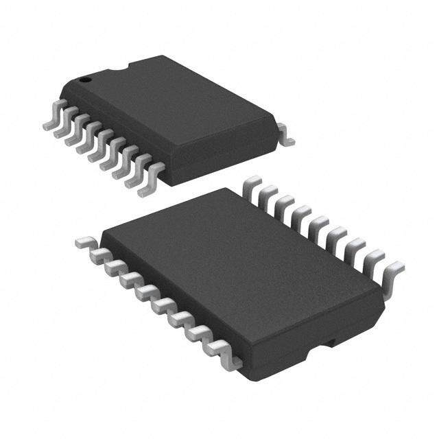
ICGOO电子元器件商城为您提供PI5C3245QE由Pericom设计生产,在icgoo商城现货销售,并且可以通过原厂、代理商等渠道进行代购。 PI5C3245QE价格参考。PericomPI5C3245QE封装/规格:逻辑 - 信号开关,多路复用器,解码器, Bus Switch 8 x 1:1 20-QSOP。您可以下载PI5C3245QE参考资料、Datasheet数据手册功能说明书,资料中有PI5C3245QE 详细功能的应用电路图电压和使用方法及教程。
| 参数 | 数值 |
| 产品目录 | 集成电路 (IC) |
| 描述 | IC 8BIT 2PORT BUS SWITCH 20QSOP |
| 产品分类 | |
| 品牌 | Pericom |
| 数据手册 | |
| 产品图片 |
|
| 产品型号 | PI5C3245QE |
| rohs | 无铅 / 符合限制有害物质指令(RoHS)规范要求 |
| 产品系列 | - |
| 产品目录页面 | |
| 供应商器件封装 | 20-QSOP |
| 包装 | 管件 |
| 安装类型 | 表面贴装 |
| 封装/外壳 | 20-SSOP(0.154",3.90mm 宽) |
| 工作温度 | -40°C ~ 85°C |
| 标准包装 | 55 |
| 独立电路 | 1 |
| 电压-电源 | 4.75 V ~ 5.25 V |
| 电压源 | 单电源 |
| 电流-输出高,低 | - |
| 电路 | 8 x 1:1 |
| 类型 | FET 总线开关 |





- 商务部:美国ITC正式对集成电路等产品启动337调查
- 曝三星4nm工艺存在良率问题 高通将骁龙8 Gen1或转产台积电
- 太阳诱电将投资9.5亿元在常州建新厂生产MLCC 预计2023年完工
- 英特尔发布欧洲新工厂建设计划 深化IDM 2.0 战略
- 台积电先进制程称霸业界 有大客户加持明年业绩稳了
- 达到5530亿美元!SIA预计今年全球半导体销售额将创下新高
- 英特尔拟将自动驾驶子公司Mobileye上市 估值或超500亿美元
- 三星加码芯片和SET,合并消费电子和移动部门,撤换高东真等 CEO
- 三星电子宣布重大人事变动 还合并消费电子和移动部门
- 海关总署:前11个月进口集成电路产品价值2.52万亿元 增长14.8%

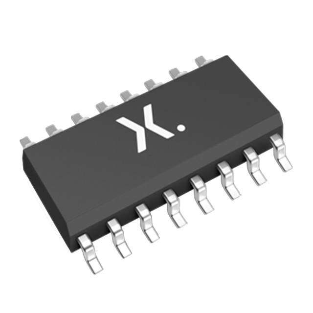


PDF Datasheet 数据手册内容提取
A product Line of Diodes Incorporated PI5C3245 8-Bit, 2-Port Bus Switch Features Description ÎÎNear-Zero propagation delay Diodes' PI5C3245 is a 8-bit, 2-port bus switch designed with a ÎÎ5Ω switches connect inputs to outputs low On-Resistance (5Ω) allowing inputs to be connected directly to outputs. The bus switch creates no additional propagational ÎÎDirect bus connection when switches are on delay or additional ground bounce noise. The switches are turned ÎÎUltra Low Quiescent Power (0.2μA typical) on by the Bus Enable (BE) input signal. The pinout is compatible à Ideally suited for notebook applications with PI74FCT245T (Octal Bidirectional Transceiver). ÎÎPin compatible with 74 Series 245 logic devices ÎÎ-Totally Lead-Free & Fully RoHS Compliant (Notes 1 & 2) Pin Configuration ÎÎ-Halogen and Antimony Free. “Green” Device (Note 3) ÎÎPackaging (Pb-free & Green): à 20-pin 173-mil wide plastic TSSOP (L) NC 1 20 VCC à 20-pin 150-mil wide plastic QSOP (Q) A0 2 19 BE A1 3 18 B0 Block Diagram A2 4 17 B1 A0 B0 A3 5 16 B2 A4 6 15 B3 A5 7 14 B4 A7 B7 A6 8 13 B5 A7 9 12 B6 GND 10 11 B7 BE Truth Table(1) Pin Description Function BE A0-7 Pin Name Description Disconnect H Hi-Z BE Bus Enable Input (Active LOW) Connect L B0-7 A0-7 Bus A Note: 1. H = High Voltage Level B0-7 Bus B L = Low Voltage Level Hi-Z = High Impedance GND Ground VCC Power Notes: 1. No purposely added lead. Fully EU Directive 2002/95/EC (RoHS), 2011/65/EU (RoHS 2) & 2015/863/EU (RoHS 3) compliant. 2. See https://www.diodes.com/quality/lead-free/ for more information about Diodes Incorporated’s definitions of Halogen- and Antimony-free, "Green" and Lead-free. 3. Halogen- and Antimony-free "Green” products are defined as those which contain <900ppm bromine, <900ppm chlorine (<1500ppm total Br + Cl) and <1000ppm antimony compounds. PI5C3245 www.diodes.com August 2019 1 Document Number DS42197 Rev 1-2 Diodes Incorporated
A product Line of Diodes Incorporated PI5C3245 Absolute Maximum Ratings (Above which useful life may be impaired. For user guidelines, not tested.) Note: Storage Temperature ..........................................................–65°C to +150°C Ambient Temperature with Power Applied .....................–40°C to +85°C Stresses greater than those listed under MAXIMUM RATINGS may cause permanent damage to the device. This is a stress rating Supply Voltage to Ground Potential (Inputs&Vcc Only) ....–0.5V to 7V only and functional operation of the device at these or any other Supply Voltage to Ground Potential (Outputs&D/O Only) –0.5V to 7V conditions above those indicated in the operational sections of this specification is not implied. Exposure to absolute maximum DC Input Voltage .......................................................................–0.5V to 7V rating conditions for extended periods may affect reliability. DC Output Current ...........................................................................120mA Power Dissipation ..................................................................................0.5W DC Electrical Characteristics (Over the Operating Range, T = –40°C to +85°C, V = 5V ±5%) A CC Parameters Description Test Conditions(1) Min. Typ. (2) Max. Units VIH Input HIGH Voltage Guaranteed Logic HIGH Level 2.0 V VIL Input LOW Voltage Guaranteed Logic LOW Level -0.5 0.8 V IIH Input HIGH Current VCC = Max., VIN = VCC ±1 μA IIL Input LOW Current VCC = Max., VIN = GND ±1 μA IOZH High Impedance Output Current 0 ≤ A, B ≤ VCC ±1 μA VIK Clamp Diode Voltage VCC = Min, IIN = -18mA -0.7 -1.2 V IOS Short Circuit Current(3) A (B) = 0V, B (A) = VCC 100 mA VH Input Hysteresis at Control Pins 150 mV VCC = Min, VIN = 0.0V, ION = 48 mA 5 7 RON Switch On Resistance(4) Ω VCC = Min, VIN = 2.4V, ION = 15 mA 10 15 Notes: 1. For Max. or Min. conditions, use appropriate value specified under Electrical Characteristics for the applicable device type. 2. Typical values are at VCC = 5.0V, TA = 25°C ambient and maximum loading. 3. Not more than one output should be shorted at one time. Duration of the test should not exceed one second. 4. Measured by the voltage drop between A and B pin at indicated current through the switch. ON resistance is determined by the lower of the voltages on the two (A,B) pins. Capacitance (T = 25°C, f = 1 MHz) A Parameters(1) Description Test Conditions Typ. Units CIN Input Capacitance VIN = 0V 6 pF COFF A/B Capacitance, Switch Off VIN = 0V 6 pF CON A/B Capacitance, Switch On VIN = 0V 8 pF Notes: 1. This parameter is determined by device characterization but is not production tested. PI5C3245 www.diodes.com August 2019 2 Document Number DS42197 Rev 1-2 Diodes Incorporated
A product Line of Diodes Incorporated PI5C3245 Power Supply Characteristics Parameters Description Test Conditions(1) Min. Typ.(2) Max. Units Quiescent Power Supply ICC Current VCC = Max. VIN = GND or VCC 0.1 3.0 μA Supply Current @ Input ΔICC HIGH VCC = Max. VIN = 3.4V(3) 2.5 mA VCC = Max. A and B Pins Open Supply Current per mA/ ICCD Input per MHz(4) BE = GND 0.25 MHz Control Input Toggling 50% Duty Cycle Notes: 1. For Max. or Min. conditions, use appropriate value specified under Electrical Characteristics for the applicable device. 2. Typical values are at VCC = 5.0V, +25°C ambient. 3. Per TTL driven input (VIN = 3.4V, control inputs only); A and B pins do not contribute to Icc. 4. This current applies to the control inputs only and represent the current required to switch internal capacitance at the specified frequency. The A and B inputs generate no significant AC or DC currents as they transition. This parameter is not tested, but is guaranteed by design. Switching Characteristics over Operating Range Com. Parameters Description Test Conditions Min Max Units tPLH Propagation Delay(1,2) 0.25 tPHL Ax to Bx, Bx to Ax tPZH Bus Enable Time CL = 50 pF 1.5 6.5 ns tPZL BE to Ax or Bx RL = 500Ω tPHZ Bus Disable Time 1.5 5.5 tPLZ BE to Ax or Bx Notes: 1. This parameter is guaranteed but not tested on Propagation Delays. 2. The bus switch contributes no propagational delay other than the RC delay of the On-Resistance of the switch and the load capacitance. The time constant for the switch alone is of the order of 0.25 ns for 50 pF load. Since this time constant is much smaller than the rise/fall times of typical driving signals, it adds very little propagational delay to the system. Propagational delay of the bus switch when used in a system is determined by the driving circuit on the driving side of the switch and its interaction with the load on the driven side. PI5C3245 www.diodes.com August 2019 3 Document Number DS42197 Rev 1-2 Diodes Incorporated
A product Line of Diodes Incorporated PI5C3245 Packaging Mechanical: 20-TSSOP (L20) 16-0074 PI5C3245 www.diodes.com August 2019 4 Document Number DS42197 Rev 1-2 Diodes Incorporated
A product Line of Diodes Incorporated PI5C3245 Packaging Mechanical: 20-QSOP (Q20) 16-0057 For latest package info. please check: http://www.diodes.com/design/support/packaging/pericom-packaging/packaging-mechanicals-and-thermal-characteristics/ Ordering Information Ordering Code Package Code Package Description PI5C3245LEX L 20-pin 173mil Wide (TSSOP) PI5C3245QEX Q 20-pin 150mil Wide (QSOP) Notes: 1. No purposely added lead. Fully EU Directive 2002/95/EC (RoHS), 2011/65/EU (RoHS 2) & 2015/863/EU (RoHS 3) compliant. 2. See https://www.diodes.com/quality/lead-free/ for more information about Diodes Incorporated’s definitions of Halogen- and Antimony-free, "Green" and Lead-free. 3. Halogen- and Antimony-free "Green” products are defined as those which contain <900ppm bromine, <900ppm chlorine (<1500ppm total Br + Cl) and <1000ppm antimony compounds. 4. E = Pb-free and Green 5. X suffix = Tape/Reel PI5C3245 www.diodes.com August 2019 5 Document Number DS42197 Rev 1-2 Diodes Incorporated
A product Line of Diodes Incorporated PI5C3245 IMPORTANT NOTICE DIODES INCORPORATED MAKES NO WARRANTY OF ANY KIND, EXPRESS OR IMPLIED, WITH REGARDS TO THIS DOCUMENT, INCLUDING, BUT NOT LIMITED TO, THE IMPLIED WARRANTIES OF MERCHANTABILITY AND FITNESS FOR A PARTICULAR PURPOSE (AND THEIR EQUIVALENTS UNDER THE LAWS OF ANY JURISDICTION). Diodes Incorporated and its subsidiaries reserve the right to make modifications, enhancements, improvements, corrections or other changes without further no- tice to this document and any product described herein. Diodes Incorporated does not assume any liability arising out of the application or use of this document or any product described herein; neither does Diodes Incorporated convey any license under its patent or trademark rights, nor the rights of others. Any Customer or user of this document or products described herein in such applications shall assume all risks of such use and will agree to hold Diodes Incorporated and all the companies whose products are represented on Diodes Incorporated website, harmless against all damages. Diodes Incorporated does not warrant or accept any liability whatsoever in respect of any products purchased through unauthorized sales channel. Should Customers purchase or use Diodes Incorporated products for any unintended or unauthorized application, Customers shall indemnify and hold Diodes Incorporated and its representatives harmless against all claims, damages, expenses, and attorney fees arising out of, directly or indirectly, any claim of personal injury or death associated with such unintended or unauthorized application. Products described herein may be covered by one or more United States, international or foreign patents pending. Product names and markings noted herein may also be covered by one or more United States, international or foreign trademarks. This document is written in English but may be translated into multiple languages for reference. Only the English version of this document is the final and determi- native format released by Diodes Incorporated. LIFE SUPPORT Diodes Incorporated products are specifically not authorized for use as critical components in life support devices or systems without the express written approval of the Chief Executive Officer of Diodes Incorporated. As used herein: A. Life support devices or systems are devices or systems which: 1. are intended to implant into the body, or 2. support or sustain life and whose failure to perform when properly used in accordance with instructions for use provided in the labeling can be reasonably expected to result in significant injury to the user. B. A critical component is any component in a life support device or system whose failure to perform can be reasonably expected to cause the failure of the life support device or to affect its safety or effectiveness. Customers represent that they have all necessary expertise in the safety and regulatory ramifications of their life support devices or systems, and acknowledge and agree that they are solely responsible for all legal, regulatory and safety-related requirements concerning their products and any use of Diodes Incorporated products in such safety-critical, life support devices or systems, notwithstanding any devices- or systems-related information or support that may be provided by Diodes Incorporated. Further, Customers must fully indemnify Diodes Incorporated and its representatives against any damages arising out of the use of Diodes Incorporated products in such safety-critical, life support devices or systems. Copyright © 2016, Diodes Incorporated www.diodes.com PI5C3245 www.diodes.com August 2019 6 Document Number DS42197 Rev 1-2 Diodes Incorporated

 Datasheet下载


