ICGOO在线商城 > 射频/IF 和 RFID > RF 开关 > PE4251MLI-Z

 Datasheet下载
- 型号: PE4251MLI-Z
- 制造商: Peregrine
- 库位|库存: xxxx|xxxx
- 要求:
| 数量阶梯 | 香港交货 | 国内含税 |
| +xxxx | $xxxx | ¥xxxx |
查看当月历史价格
查看今年历史价格
PE4251MLI-Z产品简介:
ICGOO电子元器件商城为您提供PE4251MLI-Z由Peregrine设计生产,在icgoo商城现货销售,并且可以通过原厂、代理商等渠道进行代购。 PE4251MLI-Z价格参考。PeregrinePE4251MLI-Z封装/规格:RF 开关, RF Switch IC General Purpose SPDT 3GHz 50Ohm 8-MSOP-EP。您可以下载PE4251MLI-Z参考资料、Datasheet数据手册功能说明书,资料中有PE4251MLI-Z 详细功能的应用电路图电压和使用方法及教程。
| 参数 | 数值 |
| 产品目录 | |
| 描述 | IC RF SWITCH SPDT 8-MSOP |
| 产品分类 | |
| IIP3 | 59dBm |
| 品牌 | Peregrine Semiconductor |
| 数据手册 | |
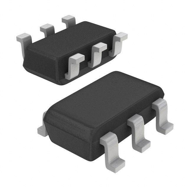
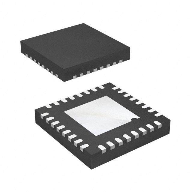
| 产品图片 |
|
| P1dB | 30.5dBm (标准) IP1dB |
| 产品型号 | PE4251MLI-Z |
| RF类型 | 通用 |
| rohs | 无铅 / 符合限制有害物质指令(RoHS)规范要求 |
| 产品系列 | UltraCMOS®,HaRP™ |
| 供应商器件封装 | 8-MSOP |
| 其它名称 | 1046-1018-1 |
| 包装 | 剪切带 (CT) |
| 封装/外壳 | 8-VSSOP,8-MSOP(0.118",3.00mm 宽)裸焊盘 |
| 工作温度 | -40°C ~ 85°C |
| 拓扑 | 吸收性 |
| 插损@频率 | 0.75dB @ 3GHz |
| 标准包装 | 1 |
| 特性 | 直流隔离,单双线路控制 |
| 电压-电源 | 3 V ~ 3.6 V,4.5 V ~ 5.5 V |
| 电路 | SPDT |
| 阻抗 | 50 欧姆 |
| 隔离@频率 | 43dB @ 3GHz (标准) |
| 频率 -上 | 3GHz |
| 频率 -下 | 10MHz |


- 商务部:美国ITC正式对集成电路等产品启动337调查
- 曝三星4nm工艺存在良率问题 高通将骁龙8 Gen1或转产台积电
- 太阳诱电将投资9.5亿元在常州建新厂生产MLCC 预计2023年完工
- 英特尔发布欧洲新工厂建设计划 深化IDM 2.0 战略
- 台积电先进制程称霸业界 有大客户加持明年业绩稳了
- 达到5530亿美元!SIA预计今年全球半导体销售额将创下新高
- 英特尔拟将自动驾驶子公司Mobileye上市 估值或超500亿美元
- 三星加码芯片和SET,合并消费电子和移动部门,撤换高东真等 CEO
- 三星电子宣布重大人事变动 还合并消费电子和移动部门
- 海关总署:前11个月进口集成电路产品价值2.52万亿元 增长14.8%


PDF Datasheet 数据手册内容提取
Product Specification PE4251 UltraCMOS® SPDT RF Switch Product Description 10–4000 MHz, Absorptive The PE4251 is a HaRP™ technology-enhanced absorptive Features single pole double throw (SPDT) RF switch for use in general • HaRP™ technology enhanced switching applications and mobile infrastructure. This device • Low insertion loss: 0.60 dB @ 1000 MHz offers a flexible supply voltage of 3.3/5V, single-pin or • complementary pin control inputs and 4 kV ESD tolerance. It High isolation: 62 dB @ 1000 MHz presents a simple alternative solution to pin diode and • P1dB typical: +30.5 dBm mechanical relay switches. • IIP3 typical: +59 dBm • Peregrine’s HaRP™ technology enhancements deliver high Fast switching time: 150 ns linearity and exceptional performance. It is an innovative • Flexible supply voltage: 3.3V ±10% or feature of the UltraCMOS® process, providing performance 5.0V ±10% supply (see Table 3) superior to GaAs with the economy and integration of • Excellent ESD protection: 4000V HBM conventional CMOS. • No blocking capacitors required Figure 1. Functional Diagram • Single pin or complementary control inputs RFC D S E RF1 RF2 Figure 2. Package Type ESD ESD 8-lead MSOP with exposed paddle 50Ω CMOS 50Ω Control Driver V1 V2 Table 1. Target Electrical Specifications Temp = +25 °C, V = 3.3V or 5.0V DD Parameter Condition Min Typ Max Unit Operation frequency1 10 4000 MHz 10 MHz 0.55 0.60 dB 1000 MHz 0.60 0.70 dB Insertion loss (RF1/RF2) 2000 MHz 0.75 0.85 dB 3000 MHz 0.75 0.90 dB 4000 MHz 1.0 dB 1000 MHz 61 62 dB 2000 MHz 51 53 dB Isolation (RFC to RF1/RF2) 3000 MHz 42 43 dB 4000 MHz 37 dB 1000 MHz 26 dB 2000 MHz 23 dB Return loss 3000 MHz 22 dB 4000 MHz 19 dB Input 1dB compression2 50–4000 MHz 30.5 dBm Input IP3 50–4000 MHz, +18 dBm per tone, 5 MHz spacing 59 dBm Switching time 50% CTRL to 10/90% RF 150 300 ns Notes: 1. Device linearity will begin to degrade below 10 MHz. 2. Absolute maximum rating of PIN = 27 dBm. Document No. DOC-18314-2 │ www.psemi.com ©2008–2015 Peregrine Semiconductor Corp. All rights reserved. Page 1 of 10
PE4251 Product Specification Table 1A. Target Electrical Specifications Temp = +125 °C, V = 3.3V or 5.0V DD Parameter Condition Min Typ Max Unit Operation frequency 50 4000 MHz 50 MHz 0.65 dB 1000 MHz 0.75 dB Insertion loss (RF1/RF2) 2000 MHz 0.90 dB 3000 MHz 1.05 dB 4000 MHz 1.2 dB 1000 MHz 62 dB 2000 MHz 52 dB Isolation (RFC to RF1/RF2) 3000 MHz 43 dB 4000 MHz 36 dB 1000 MHz 24 dB 2000 MHz 23 dB Return loss 3000 MHz 19 dB 4000 MHz 18 dB Input 1dB compression* 50–4000 MHz 30.5 dBm Input IP3 50–4000 MHz, +18 dBm per tone, 5 MHz spacing 57 dBm Switching time 50% CTRL to 10/90% RF 200 ns Note: * Absolute maximum rating of PIN = 22 dBm. ©2008–2015 Peregrine Semiconductor Corp. All rights reserved. Document No. DOC-18314-2 │ UltraCMOS® RFIC Solutions Page 2 of 10
PE4251 Product Specification Figure 3. Pin Configuration (Top View) Table 4. Absolute Maximum Ratings Symbol Parameter/Condition Min Max Unit V2 1 8 RF2 VDD Power supply voltage 3 5.5 V V1 2 7 GND VI Voltage on any control input –0.3 5.5 V 425 TST Storage temperature range –65 +150 °C RFC 3 1 6 GND RF input power (50Ω) PIN 10 MHz–4 GHz, +85 °C 27 dBm 50 MHz–4 GHz, +125 °C 22 dBm NG/CN Dor 4 5 RF1 VESD EESSDD vvoollttaaggee,, HMBMM ( machine model) 4205000 VV Note: 1. Human body model (MIL_STD 883 Method 3015). 2. Machine model (JEDEC JESD22-A115). Exposed ground paddle Exceeding absolute maximum ratings may cause Table 2. Pin Descriptions permanent damage. Operation should be Pin # Pin Name Description restricted to the limits in the Operating Ranges This pin supports two interface options: table. Operation between operating range Single-pin control mode. A nominal 3-volt maximum and absolute maximum for extended supply connection is required. 1 V2 Complementary-pin control mode. A periods may reduce reliability. complementary CMOS control signal to V1 is supplied to this pin. Latch-Up Immunity 2 V1 Switch control input, CMOS logic level. 3 RFC RF common port.* Unlike conventional CMOS devices, UltraCMOS 4 N/C or GND No connect or ground devices are immune to latch-up. 5 RF1 RF1 port.* Ground connection. Traces should be Electrostatic Discharge (ESD) Precautions 6 GND physically short and connected to ground plane for best performance. When handling this UltraCMOS device, observe Ground connection. Traces should be 7 GND physically short and connected to ground the same precautions that you would use with plane for best performance. other ESD-sensitive devices. Although this device 8 RF2 RF2 port.* contains circuitry to protect it from damage due to Exposed ground paddle. Ground for Paddle GND ESD, precautions should be taken to avoid proper device operation exceeding the specified rating. Note: * All RF pins must be DC blocked with an external series capacitor or held at 0 VDC. Switching Frequency Table 3. Operating Ranges The PE4251 has a maximum 25 kHz switching Parameter Min Typ Max Unit rate. V power supply 3.0 3.3 3.6 V DD voltage* 4.5 5.0 5.5 V Moisture Sensitivity Level I power supply current DD VDD = VCNTL= 3.3V 55 60 µA The moisture sensitivity level rating for the V = V = 5.0V 75 80 µA DD CNTL PE4251 in the 8-lead MSOP package is MSL1. Control voltage high 0.8 × V V DD Control voltage low 0.2 × V V DD P RF input power (50Ω) IN 10 MHz–4 GHz, +85 °C 27 dBm 50 MHz–4 GHz, +125 °C 22 dBm TOP operating –40 +25 +125 °C temperature range TST storage temperature –65 +25 +150 °C range Note: * Customer must choose either 3.3V or 5.0V power supply range. Document No. DOC-18314-2 │ www.psemi.com ©2008–2015 Peregrine Semiconductor Corp. All rights reserved. Page 3 of 10
PE4251 Product Specification Table 5. Single-pin Control Logic Truth Table Control Logic Input Control Voltages Signal Path The PE4251 is a versatile RF CMOS switch that supports two operating control modes: single-pin Pin 1 (V2) = V DD RFC to RF1 Pin 2 (V1) = High control mode and complementary-pin control mode. Pin 1 (V2) = V DD RFC to RF2 Pin 2 (V1) = Low Single-pin control mode enables the switch to Table 6. Complementary-pin Control Logic operate with a single control pin (pin 2) supporting Truth Table a +3.3 or 5.0-volt CMOS logic input, and requires a dedicated +3.3 or 5.0-volt power supply Control Voltages Signal Path connection (pin 1). This mode of operation Pin 1 (V2 ) = Low RFC to RF1 reduces the number of control lines required and Pin 2 (V1) = High simplifies the switch control interface typically Pin 1 (V2) = High RFC to RF2 derived from a CMOS μProcessor I/O port. Pin 2 (V1) = Low Complementary-pin control mode allows the switch to operate using complementary control pins V1 and V2 (pins 2 & 1), that can be directly driven by +3.3 or 5.0-volt CMOS logic or a suitable μProcessor I/O port. This enables the PE4251 to operate in positive control voltage mode within the PE4251 operating limits. ©2008–2015 Peregrine Semiconductor Corp. All rights reserved. Document No. DOC-18314-2 │ UltraCMOS® RFIC Solutions Page 4 of 10
PE4251 Product Specification Evaluation Kit Figure 4. Evaluation Board Layouts The SPDT switch evaluation kit board was designed to ease customer evaluation of the PE4251 SPDT switch. The RF common port is connected through a 50Ω transmission line to the bottom SMA connector, J3. Port 1 and Port 2 are connected through 50Ω transmission lines to two SMA connectors on either side of the board, J4 and J2. A through transmission line connects SMA connectors J5 and J6. This transmission line can be used to estimate the loss of the PCB over the environmental conditions being evaluated. The board is constructed of a two metal layer FR4 material with a total thickness of 0.0322”. The bottom layer provides ground for the RF transmission lines. The transmission lines were designed using a coplanar waveguide with ground plane model using a trace width of 0.033”, trace gaps of 0.010”, dielectric thickness of 0.028”, copper thickness of 0.0021” and ε of 4.3. r J1 provides a means for controlling the DC inputs to the device. The second-to-bottom lower right pin (J1–3) is connected to the device V1 input. The second-to-top upper right pin (J1–7) is connected to the device V2 input. Footprints for decoupling capacitors are provided on both V1 and V2 traces. It is the responsibility of the customer to determine proper supply decoupling for PRT-53366 their design application. Removing these components from the evaluation board has not been shown to degrade RF performance. Figure 5. Evaluation Board Schematic NOTES: J1 1. USE 101-0337-02 PCB. HEADER 2 X 5 PIN 246 246 135 135 2. CTCOAOU NDTTAIAOMINNA:SG PEA BRYT ESL AENCTDR AOSSSTEAMTBICL IDEISS CSUHSACREGPET I(BESLED) 108 810 79 79 3. A33LLM TILR AWNIDSTMHIS, I1O0NM LILIN GEASP ASR, 2E8:MIL CORE DIELECTRIC 4.3 Er AND 2.1MIL Cu C1 R1 C2 R2 R3 THICKNESS. 100pF DNI 100pF 0 OHM 0 OHM J2 SMASM U1 MSOP 1 JS3MASM 21 VV12 GNDRSF22 78 2 2 1 34 oRNrF/ CCGNDGNDRSF11 65 JS4MASM 1 2 DOC-02389 J5 J6 SMASM SMASM 1 1 2 2 Document No. DOC-18314-2 │ www.psemi.com ©2008–2015 Peregrine Semiconductor Corp. All rights reserved. Page 5 of 10
PE4251 Product Specification Figure 6. Insertion Loss: RFC–RF @ +25 °C Figure 7. Insertion Loss: RFC–RF @ 3.3V 3.0 V 3.3 V 3.6 V 4.5 V 5.0 V 5.5 V - 40°C +25°C +85°C 0 0 -0.5 -0.5 B) -1 B) -1 d d s (-1.5 s (-1.5 s s o o n L -2 n L -2 o o erti-2.5 erti-2.5 s s In -3 In -3 -3.5 -3.5 -4 -4 0 500 1000 1500 2000 2500 3000 3500 4000 0 500 1000 1500 2000 2500 3000 3500 4000 Frequency (MHz) Frequency (MHz) Figure 8. Isolation: RFC–RF @ +25 °C Figure 9. Isolation: RFC–RF @ 3.3V 3.0 V 3.3 V 3.6 V 4.5 V 5.0 V 5.5 V - 40°C +25°C +85°C 0 0 -10 -10 -20 -20 -30 -30 Isolation (dB) ----76540000 Isolation (dB) ----76540000 -80 -80 -90 -90 -100 -100 0 500 1000 1500 2000 2500 3000 3500 4000 0 500 1000 1500 2000 2500 3000 3500 4000 Frequency (MHz) Frequency (MHz) ©2008–2015 Peregrine Semiconductor Corp. All rights reserved. Document No. DOC-18314-2 │ UltraCMOS® RFIC Solutions Page 6 of 10
PE4251 Product Specification Figure 10. Return Loss at Active Port @ +25 °C Figure 11. Return Loss at Active Port @ 3.3V 3.0 V 3.3 V 3.6 V 4.5 V 5.0 V 5.5 V - 40°C +25°C +85°C 0 0 -5 -5 -10 -10 B)-15 B)-15 d d s (-20 s (-20 s s Lo-25 Lo-25 n n ur-30 ur-30 Ret-35 Ret-35 -40 -40 -45 -45 -50 -50 0 500 1000 1500 2000 2500 3000 3500 4000 0 500 1000 1500 2000 2500 3000 3500 4000 Frequency (MHz) Frequency (MHz) Document No. DOC-18314-2 │ www.psemi.com ©2008–2015 Peregrine Semiconductor Corp. All rights reserved. Page 7 of 10
PE4251 Product Specification Figure 12. Package Drawing 8-lead MSOP 0.65 A 3.00 0.10 C (x8) 1.95 (2X) 2.36 B 8 5 4.20 1.75 5.50 3.00 4.90 1.70±0.05 1.75 1.70±0.05 0.10 C 1 4 1.30 (2X) PIN #1 CORNER 0.30±0.05 0.35 (x8) (x8) 0.65 (x8) TOP VIEW BOTTOM VIEW RECOMMENDED LAND PATTERN 0.86±0.05 DOC-01889 0.10 C 0.10 C A B ALL FEATURES 0.05 C SEATING PLANE 0.10±0.05 C SIDE VIEW 0.15±0.05 (x8) 0.55±0.10 (x8) FRONT VIEW ©2008–2015 Peregrine Semiconductor Corp. All rights reserved. Document No. DOC-18314-2 │ UltraCMOS® RFIC Solutions Page 8 of 10
PE4251 Product Specification Figure 13. Top Marking Specification 4251 AAAA: Product Number, last 4 digits, Exp. LLLL: Last four digits of the Assembly lot number LLLL YWW: Date Code, last digit of the year and work week YWW Figure 14. Tape and Reel Specifications 8-lead MSOP with exposed paddle Pin1 Document No. DOC-18314-2 │ www.psemi.com ©2008–2015 Peregrine Semiconductor Corp. All rights reserved. Page 9 of 10
PE4251 Product Specification Table 7. Ordering Information Order Code Description Package Shipping Method EK4251-01 PE4251 Evaluation kit Evaluation kit 1 / Box PE4251MLI-Z PE4251 SPDT RF switch Green 8-lead MSOP, exposed paddle 3000 units / T&R Sales Contact and Information For Sales and contact information please visit www.psemi.com. Advance Information: The product is in a formative or design stage. The datasheet contains design target No patent rights or licenses to any circuits described in this datasheet are implied or granted to any third party. specifications for product development. Specifications and features may change in any manner without notice. Peregrine’s products are not designed or intended for use in devices or systems intended for surgical implant, Preliminary Specification: The datasheet contains preliminary data. Additional data may be added at a later or in other applications intended to support or sustain life, or in any application in which the failure of the date. Peregrine reserves the right to change specifications at any time without notice in order to supply the best Peregrine product could create a situation in which personal injury or death might occur. Peregrine assumes no possible product. Product Specification: The datasheet contains final data. In the event Peregrine decides to liability for damages, including consequential or incidental damages, arising out of the use of its products in change the specifications, Peregrine will notify customers of the intended changes by issuing a CNF (Customer such applications. Notification Form). The Peregrine name, logo, UltraCMOS and UTSi are registered trademarks and HaRP, MultiSwitch and DuNE The information in this datasheet is believed to be reliable. However, Peregrine assumes no liability for the use are trademarks of Peregrine Semiconductor Corp. Peregrine products are protected under one or more of the of this information. Use shall be entirely at the user’s own risk. following U.S. Patents: http://patents.psemi.com ©2008–2015 Peregrine Semiconductor Corp. All rights reserved. Document No. DOC-18314-2 │ UltraCMOS® RFIC Solutions Page 10 of 10