ICGOO在线商城 > 射频/IF 和 RFID > RF 开关 > PE42421SCAA-Z
 Datasheet下载
- 型号: PE42421SCAA-Z
- 制造商: Peregrine
- 库位|库存: xxxx|xxxx
- 要求:
| 数量阶梯 | 香港交货 | 国内含税 |
| +xxxx | $xxxx | ¥xxxx |
查看当月历史价格
查看今年历史价格
PE42421SCAA-Z产品简介:
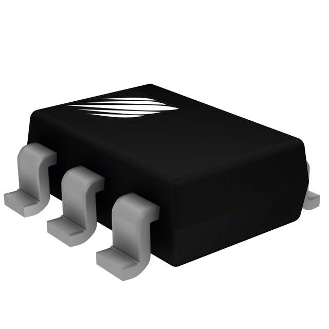
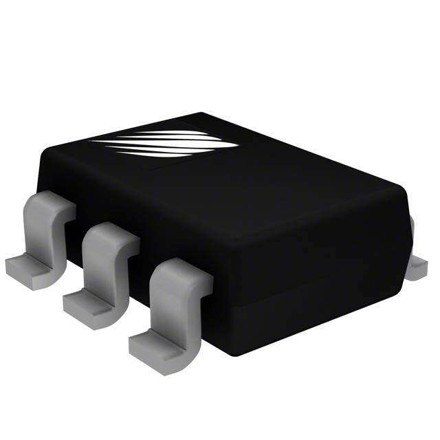
ICGOO电子元器件商城为您提供PE42421SCAA-Z由Peregrine设计生产,在icgoo商城现货销售,并且可以通过原厂、代理商等渠道进行代购。 PE42421SCAA-Z价格参考。PeregrinePE42421SCAA-Z封装/规格:RF 开关, 射频开关 IC 通用 SPDT 3GHz 50 欧姆 SC-70-6。您可以下载PE42421SCAA-Z参考资料、Datasheet数据手册功能说明书,资料中有PE42421SCAA-Z 详细功能的应用电路图电压和使用方法及教程。
pSemi品牌的RF开关型号PE42421SCAA-Z是一款高性能射频开关,适用于多种无线通信和射频应用。该器件的主要应用场景包括:

1. 蜂窝通信:在4G LTE、5G基站和用户设备中,PE42421SCAA-Z可以用于信号路径切换,确保不同频段和模式之间的高效转换。其低插入损耗和高隔离度特性,有助于提高通信系统的整体性能。

2. Wi-Fi与物联网(IoT)设备:在Wi-Fi路由器、智能家居设备和其他物联网终端中,该开关可以实现多天线选择和频段切换,支持2.4GHz和5GHz频段的灵活切换,提升设备的连接稳定性和传输速率。

3. 雷达系统:在汽车雷达、气象雷达等应用中,PE42421SCAA-Z能够快速切换发射和接收路径,确保雷达系统的实时性和准确性。其高速切换能力和宽工作频率范围,使其非常适合雷达系统的严格要求。

4. 卫星通信:在卫星地面站和移动卫星通信设备中,该开关可用于多频段信号的切换,确保不同卫星链路之间的无缝切换,提高通信的可靠性和灵活性。

5. 测试与测量设备:在射频测试仪器中,如信号发生器、频谱分析仪等,PE42421SCAA-Z可以用于内部信号路径的控制,提供精确的信号路由,确保测试结果的准确性和一致性。

6. 军事通信与电子战:在军事通信系统和电子战设备中,该开关能够实现快速的频段切换和信号路径控制,增强系统的抗干扰能力和隐蔽性。

总的来说,PE42421SCAA-Z凭借其优异的射频性能和广泛的适用性,成为众多射频系统中的关键组件,特别是在需要高频段切换和高可靠性应用的场景中表现尤为突出。
| 参数 | 数值 |
| 产品目录 | |
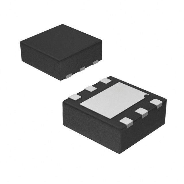
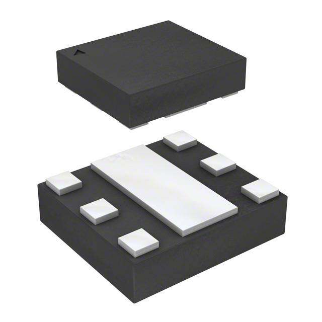
| 描述 | IC RF SWITCH SPDT 50 OHM SC70-6 |
| 产品分类 | |
| IIP3 | 55dBm (标准) |
| 品牌 | Peregrine Semiconductor |
| 数据手册 | |
| 产品图片 |
|
| P1dB | 30.5dBm (标准) IP1dB |
| 产品型号 | PE42421SCAA-Z |
| RF类型 | 通用 |
| rohs | 无铅 / 符合限制有害物质指令(RoHS)规范要求 |
| 产品系列 | UltraCMOS® |
| 供应商器件封装 | SC-70-6 |
| 其它名称 | 1046-1061-2 |
| 包装 | 带卷 (TR) |
| 封装/外壳 | 6-TSSOP,SC-88,SOT-363 |
| 工作温度 | -40°C ~ 85°C |
| 拓扑 | 反射 |
| 插损@频率 | 0.5dB @ 2GHz |
| 标准包装 | 3,000 |
| 特性 | 单双线路控制 |
| 特色产品 | http://www.digikey.cn/product-highlights/cn/zh/peregrine-pe42421-rf-switch/2967 |
| 电压-电源 | 1.8 V ~ 3.3 V |
| 电路 | SPDT |
| 阻抗 | 50 欧姆 |
| 隔离@频率 | 20dB @ 2GHz (标准) |
| 频率 -上 | 3GHz |
| 频率 -下 | 10MHz |


- 商务部:美国ITC正式对集成电路等产品启动337调查
- 曝三星4nm工艺存在良率问题 高通将骁龙8 Gen1或转产台积电
- 太阳诱电将投资9.5亿元在常州建新厂生产MLCC 预计2023年完工
- 英特尔发布欧洲新工厂建设计划 深化IDM 2.0 战略
- 台积电先进制程称霸业界 有大客户加持明年业绩稳了
- 达到5530亿美元!SIA预计今年全球半导体销售额将创下新高
- 英特尔拟将自动驾驶子公司Mobileye上市 估值或超500亿美元
- 三星加码芯片和SET,合并消费电子和移动部门,撤换高东真等 CEO
- 三星电子宣布重大人事变动 还合并消费电子和移动部门
- 海关总署:前11个月进口集成电路产品价值2.52万亿元 增长14.8%

PDF Datasheet 数据手册内容提取
Product Specification PE42421 SPDT UltraCMOS® 10 MHz – 3.0 GHz RF Switch Product Description Features The PE42421 UltraCMOS® RF switch is designed to Single-pin or complementary CMOS cover a broad range of applications from 10 MHz logic control inputs through 3000 MHz. This reflective switch integrates Low insertion loss: 0.35 dB at on-board CMOS control logic with a low voltage 1000 MHz, 0.5 dB at 2000 MHz CMOS-compatible control interface, and can be controlled using either single-pin or complementary Isolation of 30 dB at 1000 MHz, 20 dB control inputs. Using a nominal +3-volt power supply at 2000 MHz voltage, a typical input 1 dB compression point of Typical input 1 dB compression point +33.5 dBm can be achieved. of +33.5 dBm The PE42421 SPDT RF switch is manufactured on 1.8V minimum power supply voltage Peregrine’s UltraCMOS® process, a patented SC-70 package variation of silicon-on-insulator (SOI) technology on a sapphire substrate, offering the performance of GaAs with the economy and integration of conventional CMOS. Figure 1. Functional Diagram Figure 2. Package 6-lead SC-70 RFC D S E RF1 RF2 ESD ESD CMOS Control Driver CTRL CTRL or V DD 71-0015-01 Document No. 70-0396-03 │ www.psemi.com ©2010-2013 Peregrine Semiconductor Corp. All rights reserved. Page 1 of 9 Logo updated under non-rev change. Peregrine products are protected under one or more of the following U.S. Patents: http://patents.psemi.com
PE42421 Product Specification Table 1. Electrical Specifications @ +25°C, V = 3V (Z = Z = 50Ω ) DD S L Parameter Condition Minimum Typical Maximum Unit Operation Frequency1 10 MHz 3000 MHz 1000 MHz 0.35 0.45 dB Insertion Loss3 2000 MHz 0.50 0.60 dB 1000 MHz 29 30 dB Isolation 2000 MHz 19 20 dB 1000 MHz 21 22 dB Return Loss3 2000 MHz 24 27 dB ‘ON’ Switching Time 50% CTRL to 0.1 dB of final value, 1 GHz 1.50 us ‘OFF’ Switching Time 50% CTRL to 25 dB isolation, 1 GHz 1.50 us Video Feedthrough2 15 mV pp 1000 MHz @ 2.3 - 3.3V 31.5 33.5 1000 MHz @ 1.8 - 2.3V 29.5 30.5 Input 1 dB Compression dBm 2500 MHz @ 2.3 - 3.3V 28.5 30.5 2500 MHz @ 1.8 - 2.3V 28 29 Input IP3 1000 MHz, 20dBm input power 55 dBm Notes: 1. Device linearity will begin to degrade below 10 MHz 2. The DC transient at the output of any port of the switch when the control voltage is switched from Low to High or High to Low in a 50Ω test set-up, measured with 1ns risetime pulses and 500 MHz bandwidth 3. A tuning capacitor must be added to the application board to optimize the insertion loss and return loss performance. See Figure 6 for details ©2010-2013 Peregrine Semiconductor Corp. All rights reserved. Document No. 70-0396-03 │ UltraCMOS® RFIC Solutions Page 2 of 9 Logo updated under non-rev change. Peregrine products are protected under one or more of the following U.S. Patents: http://patents.psemi.com
PE42421 Product Specification Figure 3. Pin Configuration (Top View) Table 4. Absolute Maximum Ratings Symbol Parameter/Condition Min Max Unit V Power supply voltage -0.3 4.0 V DD V + V Voltage on any DC input -0.3 DD V I 0.3 T Storage temperature range -65 150 °C ST Operating temperature T -40 85 °C OP range Table 2. Pin Descriptions P Input power (50 Ω) +345 dBm IN Pin No. Pin Name Description ESD Voltage (HBM, ML_STD 883 Method 2000 V 1 RF14 RF Port1 V 3015.7) ESD Ground connection. Traces should be ESD Voltage (MM, JEDEC, 2 GND physically short and connected to ground 100 V JESD22-A114-B) plane for best performance. 3 RF24 RF Port2 Notes: 5. To maintain optimum device performance, do not exceed Max PIN at desired operating frequency (see Figure 4) 4 CTRL Switch control input, CMOS logic level. Exceeding absolute maximum ratings may cause 5 RFC4 RF Common permanent damage. Operation should be restricted to This pin supports two interface options: the limits in the Operating Ranges table. Operation Single-pin control mode. A nominal 3-volt between operating range maximum and absolute supply connection is required. 6 CTRLor V Complementary-pin control mode. A com- maximum for extended periods may reduce reliability. DD plementary CMOS control signal to CTRL is supplied to this pin. Bypassing on this Figure 4. Maximum Input Power pin is not required in this mode. Note: 4. All RF pins must be DC blocked with an external series capacitor or held at 0 VDC Table 3. Operating Ranges Parameter Min Typ Max Unit V Power Supply Voltage 1.8 3.0 3.3 V DD I Power Supply Current DD 9 20 µA (V = 3V, V = 3V) DD CNTL Control Voltage High 0.7x V V DD Control Voltage Low 0.3x V V DD Moisture Sensitivity Level The Moisture Sensitivity Level rating for the PE42421 in the SC70 package is MSL1. Latch-Up Avoidance Unlike conventional CMOS devices, UltraCMOS® Switching Frequency devices are immune to latch-up. The PE42421 has a maximum 25 kHz switching rate. Electrostatic Discharge (ESD) Precautions When handling this UltraCMOS® device, observe the same precautions that you would use with other ESD- sensitive devices. Although this device contains circuitry to protect it from damage due to ESD, precautions should be taken to avoid exceeding the specified rating. Document No. 70-0396-03 │ www.psemi.com ©2010-2013 Peregrine Semiconductor Corp. All rights reserved. Page 3 of 9 Logo updated under non-rev change. Peregrine products are protected under one or more of the following U.S. Patents: http://patents.psemi.com
PE42421 Product Specification Table 5. Single-pin Control Logic Truth Table Control Logic Input Control Voltages Signal Path The PE42421 is a versatile RF CMOS switch that supports two operating control modes; single-pin Pin 6 (V ) = V Pin 4 (CDTDRL) =D HDigh RFC to RF2 control mode and complementary-pin control mode. Pin 6 (V ) = V DD DD RFC to RF1 Pin 4 (CTRL) = Low Single-pin control mode enables the switch to Table 6. Complementary-pin Control Logic operate with a single control pin (pin 4) supporting Truth Table a +3-volt CMOS logic input, and requires a dedicated +3-volt power supply connection on pin Control Voltages Signal Path 6 (V ). This mode of operation reduces the DD number of control lines required and simplifies the Pin 6 (CTRL or V ) = Low DD RFC to RF2 switch control interface typically derived from a Pin 4 (CTRL) = High CMOS Processor I/O port. Pin 6 (CTRL or VDD) = High RFC to RF1 Pin 4 (CTRL) = Low Complementary-pin control mode allows the switch to operate using complementary control pins CTRL and CTRL (pins 4 & 6), that can be directly driven by +3-volt CMOS logic or a suitable Processor I/O port. This enables the PE42421 to be used as a potential alternate source for SPDT RF switch products used in positive control voltage mode and operating within the PE42421 operating limits. ©2010-2013 Peregrine Semiconductor Corp. All rights reserved. Document No. 70-0396-03 │ UltraCMOS® RFIC Solutions Page 4 of 9 Logo updated under non-rev change. Peregrine products are protected under one or more of the following U.S. Patents: http://patents.psemi.com
PE42421 Product Specification Evaluation Kit Figure 5. Evaluation Board Layouts Peregrine Specification 101-0162-02 The SPDT switch EK Board was designed to ease customer evaluation of Peregrine’s PE42421. The RF common port is connected through a 50Ω transmission line via the top SMA connector, J1. RF1 and RF2 are connected through 50Ω transmission lines via SMA connectors J2 and J3, respectively. A through 50Ω transmission is available via SMA connectors J4 and J5. This transmission line can be used to estimate the loss of the PCB over the environmental conditions being evaluated. The board is constructed of a two metal layer FR4 material with a total thickness of 0.031”. The bottom layer provides ground for the RF transmission lines. The transmission lines were designed using a coplanar waveguide with ground plane model using a trace width of 0.0476”, trace gaps of 0.030”, dielectric thickness of 0.028”, metal thickness of 0.0021” and ε of 4.4. r J6 and J7 provide a means for controlling DC and digital inputs to the device. J6-1 is connected to the device V or CTRL input. J7-1 is connected DD to the device CTRL input. Figure 6. Evaluation Board Schematic Peregrine Specification 102-0756-01 J4 1 1 J5 N/A N/A T-lineDescription -- Model=CPWG J7 General Comments H=28mils CNTL TW==24.17mmiillss Transmission lines connected to J1, J2, and J3 should have exactly the G=30mils 12 same electrical length Er=4.4 The path from J2 to J3 including the distance through the part should have the same length as J4 and J5 and be in parallel to J4 to J5 R2 1KOhm U1 1 J3 PE42421/SC70-6 RF2 JR1FC 1 456 CRVFDTCRDL RRGFFN__D12 213 1 1 JR2F1 C1 0.5pF 2 SEEASSYNOTE2 R1 1KOhm 1 Notes: Add two 0.5 pF caps in series to be shunted on the J1 SMA input C2 0.5pF Solder C1 side 1 to the RF trace close to the J1 pin 2 SEEASSYNOTE2 Solder C1 side 2 to C2 side 1 12 Solder C2 side 2 to ground J6 CNTLX/VDD Document No. 70-0396-03 │ www.psemi.com ©2010-2013 Peregrine Semiconductor Corp. All rights reserved. Page 5 of 9 Logo updated under non-rev change. Peregrine products are protected under one or more of the following U.S. Patents: http://patents.psemi.com
PE42421 Product Specification Typical Performance Data @ -40°C to 85°C (Unless Otherwise Noted) Figure 7. Insertion Loss Figure 8. Isolation – Input to Output Figure 9. Isolation – Output to Output Figure 10. Return Loss (Input) ©2010-2013 Peregrine Semiconductor Corp. All rights reserved. Document No. 70-0396-03 │ UltraCMOS® RFIC Solutions Page 6 of 9 Logo updated under non-rev change. Peregrine products are protected under one or more of the following U.S. Patents: http://patents.psemi.com
PE42421 Product Specification Typical Performance Data @ V = 2.3V, T = 25°C DD Figure 11. Insertion Loss Figure 12. Isolation – Input to Output Figure 13. Isolation – Output to Output Figure 14. Return Loss (Input & Output) Document No. 70-0396-03 │ www.psemi.com ©2010-2013 Peregrine Semiconductor Corp. All rights reserved. Page 7 of 9 Logo updated under non-rev change. Peregrine products are protected under one or more of the following U.S. Patents: http://patents.psemi.com
PE42421 Product Specification Figure 15. Package Drawing 6-lead SC-70 0.10 C A 2.10±0.05 (2X) 0.65 1.30 B 6 4 0.50MIN 0.10 C 1.25±0.10 2.10±0.10 1.90 0.90±0.10 0.05 C 0.10 C 1 3 SEATINGPLANE (2X) 0.05±0.05 C Pin#1Corner 0.65 0.225±0.075 0.40MIN 1.30 Top View Side View Recommended Land Pattern 181-0013 0.10 A B 0.165±0.085 ALLFEATURES 0.36±0.10 End View Figure 16. Top Marking Specification PPP = Pin 1 Indicator YWW PPP = Part Number YWW = Date Code 17-0021 ©2010-2013 Peregrine Semiconductor Corp. All rights reserved. Document No. 70-0396-03 │ UltraCMOS® RFIC Solutions Page 8 of 9 Logo updated under non-rev change. Peregrine products are protected under one or more of the following U.S. Patents: http://patents.psemi.com
PE42421 Product Specification Figure 17. Tape and Reel Specifications Pin 1 Tape Feed Direction 6 5 4 654 Top of Device 123 1 2 3 Pin 1 Device Orientation in Tape Table 7. Ordering Information Order Code Part Marking Description Package Shipping Method EK42421-01 PE42421-EK PE42421 Evaluation Kit Evaluation Kit 1 / Box PE42421SCAA-Z 421 PE42421 SPDT RF Switch Green 6-lead SC-70 3000 units / T&R Sales Contact and Information For sales and contact information please visit www.psemi.com. Advance Information: The product is in a formative or design stage. The datasheet contains design target No patent rights or licenses to any circuits described in this datasheet are implied or granted to any third party. specifications for product development. Specifications and features may change in any manner without notice. Peregrine’s products are not designed or intended for use in devices or systems intended for surgical implant, Preliminary Specification: The datasheet contains preliminary data. Additional data may be added at a later or in other applications intended to support or sustain life, or in any application in which the failure of the date. Peregrine reserves the right to change specifications at any time without notice in order to supply the best Peregrine product could create a situation in which personal injury or death might occur. Peregrine assumes no possible product. Product Specification: The datasheet contains final data. In the event Peregrine decides to liability for damages, including consequential or incidental damages, arising out of the use of its products in change the specifications, Peregrine will notify customers of the intended changes by issuing a CNF (Customer such applications. Notification Form). The Peregrine name, logo, UltraCMOS and UTSi are registered trademarks and HaRP, MultiSwitch and DuNE The information in this datasheet is believed to be reliable. However, Peregrine assumes no liability for the use are trademarks of Peregrine Semiconductor Corp. of this information. Use shall be entirely at the user’s own risk. Document No. 70-0396-03 │ www.psemi.com ©2010-2013 Peregrine Semiconductor Corp. All rights reserved. Page 9 of 9 Logo updated under non-rev change. Peregrine products are protected under one or more of the following U.S. Patents: http://patents.psemi.com