
 Datasheet下载
- 型号: PDS1-S5-S9-M-TR
- 制造商: CUI/STACK INCORPORATED
- 库位|库存: xxxx|xxxx
- 要求:
| 数量阶梯 | 香港交货 | 国内含税 |
| +xxxx | $xxxx | ¥xxxx |
查看当月历史价格
查看今年历史价格
PDS1-S5-S9-M-TR产品简介:
ICGOO电子元器件商城为您提供PDS1-S5-S9-M-TR由CUI/STACK INCORPORATED设计生产,在icgoo商城现货销售,并且可以通过原厂、代理商等渠道进行代购。 PDS1-S5-S9-M-TR价格参考。CUI/STACK INCORPORATEDPDS1-S5-S9-M-TR封装/规格:直流转换器, 隔离模块 DC/DC 转换器 1 输出 9V 111mA 4.5V - 5.5V 输入。您可以下载PDS1-S5-S9-M-TR参考资料、Datasheet数据手册功能说明书,资料中有PDS1-S5-S9-M-TR 详细功能的应用电路图电压和使用方法及教程。
| 参数 | 数值 |
| 3D型号 | http://www.cui.com/product/resource/digikey3dmodel/pds1-s5-s9-m |
| 产品目录 | |
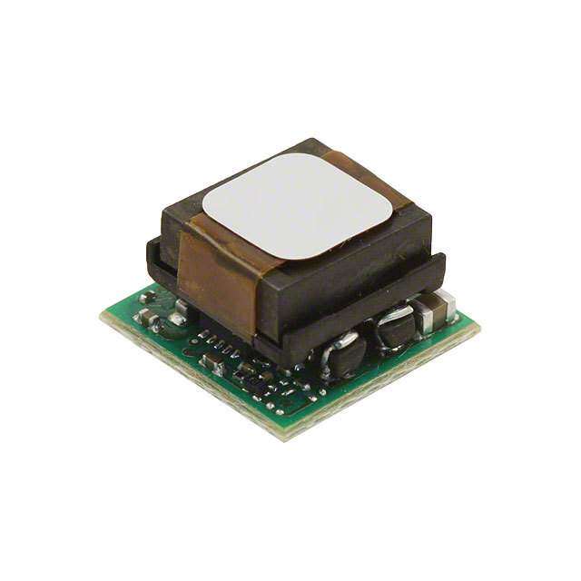
| 描述 | DC/DC CONVERTER 9V 1W |
| 产品分类 | DC DC Converters |
| 品牌 | CUI Inc |
| 数据手册 | |
| 产品图片 |
|
| 产品型号 | PDS1-S5-S9-M-TR |
| rohs | 无铅 / 符合限制有害物质指令(RoHS)规范要求 |
| RoHS指令信息 | http://www.cui.com/product/resource/digikeyrohs/pds1-m-series |
| 产品系列 | PDS1-M |
| 产品培训模块 | http://www.digikey.cn/PTM/IndividualPTM.page?site=cn&lang=zhs&ptm=25129http://www.digikey.cn/PTM/IndividualPTM.page?site=cn&lang=zhs&ptm=30294http://www.digikey.cn/PTM/IndividualPTM.page?site=cn&lang=zhs&ptm=30387http://www.digikey.cn/PTM/IndividualPTM.page?site=cn&lang=zhs&ptm=30568 |
| 其它名称 | 102-2974-1 |
| 功率(W)-制造系列 | 1W |
| 功率(W)-最大值 | 1W |
| 包装 | 剪切带 (CT) |
| 大小/尺寸 | 0.50" 长 x 0.33" 宽 x 0.29" 高 (12.7mm x 8.3mm x 7.3mm) |
| 安装类型 | 表面贴装 |
| 封装/外壳 | 8-SMD 模块(5 引线) |
| 工作温度 | -40°C ~ 105°C |
| 效率 | 80% |
| 标准包装 | 1 |
| 特性 | SCP |
| 电压-输入(最大值) | 5.5V |
| 电压-输入(最小值) | 4.5V |
| 电压-输出1 | 9V |
| 电压-输出2 | - |
| 电压-输出3 | - |
| 电压-隔离 | 1.5kV(1500V) |
| 电流-输出(最大值) | 111mA |
| 类型 | 隔离模块 |
| 输出数 | 1 |


PDF Datasheet 数据手册内容提取
For more information, please visit the product page. ddaattee 07/03/2018 ppaaggee 11 ooff 88 SERIES: PDS1-M │ DESCRIPTION: DC-DC CONVERTER FEATURES • 1 W isolated output • smaller package • single and dual unregulated outputs • 1,500 Vdc isolation • short circuit protection • extended temperature range (-40~105°C) • antistatic protection up to 8kV • high efficiency at light load • efficiency up to 82% MODEL input output output output ripple efficiency voltage voltage current power and noise2 typ range min max max typ typ (Vdc) (Vdc) (Vdc) (mA) (mA) (W) (mVp-p) (%) PDS1-S3-S3-M 3.3 2.97~3.63 3.3 30 303 1 60 69 PDS1-S3-S5-M1 3.3 2.97~3.63 5 20 200 1 60 74 PDS1-S3-D5-M 3.3 2.97~3.63 ±5 ±10 ±100 1 60 76 PDS1-S3-D12-M 3.3 2.97~3.63 ±12 ±5 ±42 1 60 77 PDS1-S3-D15-M 3.3 2.97~3.63 ±15 ±3 ±33 1 60 78 PDS1-S5-S3-M1 5 4.5~5.5 3.3 30 303 1 60 72 PDS1-S5-S5-M1 5 4.5~5.5 5 20 200 1 60 80 PDS1-S5-S9-M1 5 4.5~5.5 9 12 111 1 60 80 PDS1-S5-S12-M1 5 4.5~5.5 12 9 84 1 60 80 PDS1-S5-S15-M1 5 4.5~5.5 15 7 67 1 60 80 PDS1-S5-S24-M1 5 4.5~5.5 24 4 42 1 60 80 PDS1-S5-D5-M 5 4.5~5.5 ±5 ±10 ±100 1 60 80 PDS1-S5-D9-M 5 4.5~5.5 ±9 ±6 ±56 1 60 80 PDS1-S5-D12-M 5 4.5~5.5 ±12 ±5 ±42 1 60 79 PDS1-S5-D15-M 5 4.5~5.5 ±15 ±3 ±33 1 60 81 PDS1-S5-D24-M 5 4.5~5.5 ±24 ±2 ±21 1 60 81 PDS1-S12-S3-M1 12 10.8~13.2 3.3 30 303 1 60 72 PDS1-S12-S5-M1 12 10.8~13.2 5 20 200 1 60 80 PDS1-S12-S9-M1 12 10.8~13.2 9 12 111 1 60 80 PDS1-S12-S12-M1 12 10.8~13.2 12 9 84 1 60 80 PDS1-S12-S15-M1 12 10.8~13.2 15 7 67 1 60 80 PDS1-S12-D5-M 12 10.8~13.2 ±5 ±10 ±100 1 60 80 PDS1-S12-D9-M 12 10.8~13.2 ±9 ±6 ±56 1 60 80 PDS1-S12-D12-M 12 10.8~13.2 ±12 ±5 ±42 1 60 81 PDS1-S12-D15-M 12 10.8~13.2 ±15 ±3 ±33 1 60 81 PDS1-S12-D24-M 12 10.8~13.2 ±24 ±2 ±21 1 60 81 PDS1-S15-S15-M 15 13.5~16.5 15 7 67 1 60 80 Notes: 1. UL approved 2. Ripple and noise are measured at 20 MHz BW by “parallel cable” method with 1 μF ceramic and 10 μF electrolytic capacitors on the output. c u i . c o m
For more information, please visit the product page. CUI Inc │ SERIES: PDS1-M │ DESCRIPTION: DC-DC CONVERTER date 07/03/2018 │ page 2 of 8 MODEL input output output output ripple efficiency voltage voltage current power and noise2 (CONTINUED) typ range min max max typ typ (Vdc) (Vdc) (Vdc) (mA) (mA) (W) (mVp-p) (%) PDS1-S24-S5-M1 24 21.6~26.4 5 20 200 1 60 80 PDS1-S24-S9-M1 24 21.6~26.4 9 12 111 1 60 80 PDS1-S24-S12-M 24 21.6~26.4 12 9 84 1 60 80 PDS1-S24-S15-M1 24 21.6~26.4 15 7 67 1 60 80 PDS1-S24-S24-M1 24 21.6~26.4 24 4 42 1 60 80 PDS1-S24-D5-M 24 21.6~26.4 ±5 ±10 ±100 1 60 80 PDS1-S24-D9-M 24 21.6~26.4 ±9 ±6 ±56 1 60 80 PDS1-S24-D12-M 24 21.6~26.4 ±12 ±5 ±42 1 60 81 PDS1-S24-D15-M 24 21.6~26.4 ±15 ±3 ±33 1 60 82 PDS1-S24-D24-M 24 21.6~26.4 ±24 ±2 ±21 1 60 80 Notes: 1. UL approved 2. Ripple and noise are measured at 20 MHz BW by “parallel cable” method with 1 μF ceramic and 10 μF electrolytic capacitors on the output. PART NUMBER KEY PDS1 - SXX - XXX - M - X Base Number Input Voltage Output Output Voltage Packaging Style Package Options S = single SMT "blank" = standard D = dual TR = Tape & Reel INPUT parameter conditions/description min typ max units 3.3 Vdc input models 2.97 3.3 3.63 Vdc 5 Vdc input models 4.5 5 5.5 Vdc operating input voltage 12 Vdc input models 10.8 12 13.2 Vdc 15 Vdc input models 13.5 15 16.5 Vdc 24 Vdc input models 21.6 24 26.4 Vdc for maximum of 1 second 3.3 Vdc input models -0.7 5 Vdc 5 Vdc input models -0.7 9 Vdc surge voltage 12 Vdc input models -0.7 18 Vdc 15 Vdc input models -0.7 21 Vdc 24 Vdc input models -0.7 30 Vdc filter capacitance filter OUTPUT parameter conditions/description min typ max units for Vin change of 1% line regulation 3.3 Vdc output models ±1.5 % all other models ±1.2 % measured from 10% load to full load 3.3 Vdc output models 18 % 5 Vdc output models 12 % load regulation 9 Vdc output models 8 % 12 Vdc output models 7 % 15 Vdc output models 6 % 24 Vdc output models 5 % voltage accuracy see tolerance envelope curve switching frequency 100% load, nominal input voltage 100 kHz temperature coefficient 100% load ±0.03 %/°C c u i . c o m
For more information, please visit the product page. CUI Inc │ SERIES: PDS1-M │ DESCRIPTION: DC-DC CONVERTER date 07/03/2018 │ page 3 of 8 PROTECTIONS parameter conditions/description min typ max units 3 & 24 Vdc input models 1 s short circuit protection1 PDS1-S5-S12-M, PDS1-S5-D24-M 1 s all other models: automatic recovery Note: 1. The supply voltage must be discontinued at the end of the short circuit duration SAFETY AND COMPLIANCE parameter conditions/description min typ max units isolation voltage input to output for 1 minute at 1 mA max. 1,500 Vdc isolation resistance input to output at 500 Vdc 1,000 MΩ isolation capacitance input to output at 100 kHz/0.1 V 20 pF safety approvals2 UL 60950-1 conducted emissions CISPR32/EN55032, class B (external circuit required, see Figure 1) radiated emissions CISPR32/EN55032, class B (external circuit required, see Figure 1) IEC/EN 61000-4-2, class B, contact ±8kV (single output models) ESD IEC/EN 61000-4-2, class B, contact ±6kV (dual output models) MTBF as per MIL-HDBK-217F @ 25 °C 3,500,000 hours RoHS 2011/65/EU Note: 2. See specific models noted on pages 1 & 2 ENVIRONMENTAL parameter conditions/description min typ max units operating temperature see derating curve -40 105 °C storage temperature -55 125 °C storage humidity non-condensing 95 % temperature rise at full load, Ta=25°C 25 °C SOLDERABILITY parameter conditions/description min typ max units hand soldering 1.5 mm from case for 10 seconds 300 °C reflow soldering see reflow soldering profile 245 °C 224550 Peak.Temp 245˚(cid:3)C(Max.) 217 200 60Sec Max ) (>217˚(cid:3)C) C ˚ ( e 150 r u t a r e 100 p m e T 50 0 Time (sec.) c u i . c o m
For more information, please visit the product page. CUI Inc │ SERIES: PDS1-M │ DESCRIPTION: DC-DC CONVERTER date 07/03/2018 │ page 4 of 8 MECHANICAL parameter conditions/description min typ max units single output models: 12.7 x 8.30 x 7.25 mm dimensions dual output models: 15.24 x 8.30 x 7.25 mm case material epoxy resin (UL94-V0) single output models 1.6 g weight dual output models 2.0 g MECHANICAL DRAWING SINGLE OUTPUT MODELS units: mm[inch] tolerance: ±0.25[±0.010] pin section tolerance: ±0.10[±0.004] PIN CONNECTIONS PIN Function 1 GND 2 Vin 4 0V 5 +Vo 8 NC c u i . c o m
For more information, please visit the product page. CUI Inc │ SERIES: PDS1-M │ DESCRIPTION: DC-DC CONVERTER date 07/03/2018 │ page 5 of 8 MECHANICAL DRAWING (CONTINUED) DUAL OUTPUT MODELS units: mm[inch] tolerance: ±0.25[±0.010] pin section tolerance: ±0.10[±0.004] PIN CONNECTIONS PIN Function 1 GND 2 Vin 4 0V 5 -Vo 7 +Vo 10 NC c u i . c o m
For more information, please visit the product page. CUI Inc │ SERIES: PDS1-M │ DESCRIPTION: DC-DC CONVERTER date 07/03/2018 │ page 6 of 8 DERATING CURVES Tolerance Envelope Curve Tolerance Envelope Curve (3.3 Vdc output only) (all other models) %) 10 %) 15 Output Voltage Accuracy ( --11-50505 Typical LoaMMdi anLxine R-1-7a1..055ted Output Voltage Output Voltage Accuracy (-11- 05500 Typical LoaMMdai nxLine --R272.a..555ted Output Voltage 10 20 40 60 80 100 10 20 40 60 80 100 Output Current Percentage (%) Output Current Percentage (%) (Nominal Input Voltage) (Nominal Input Voltage) Temperature Derating Curve 100 ) 80 % ( d 60 oa Safe operating area L 40 20 -40 -20 0 20 40 60 80 100105120 Ambient Temperature (°C) EMC RECOMMENDED CIRCUIT Figure 1 Table 1 LDM Vin Vin +Vo Recommended external circuit components DC/DC LOAD Single Outputs Vin C1 C2 C1 C21 LDM CY2 (Vdc) GND GND 0V 3.3 4.7μF/50V - 6.8μH - 5 4.7μF/50V - 6.8μH - 12 4.7μF/50V - 6.8μH - 15 4.7μF/50V - 6.8μH 1nF/2kV LDM 24 4.7μF/50V - 6.8μH 1nF/2kV Vin Vin +Vo Dual Outputs Note: 1. See Cout values in Tables 2 & 3. 2. 24 Vdc output models require CY also. DC/DC LOAD C1 C2 GND GND -Vo CY c u i . c o m
For more information, please visit the product page. CUI Inc │ SERIES: PDS1-M │ DESCRIPTION: DC-DC CONVERTER date 07/03/2018 │ page 7 of 8 APPLICATION NOTES 1. Output load requirement To ensure this module can operate efficiently and reliably, the minimum output load may not be less than 10% of the full load during operation. If the actual output power is low, connect a resistor at the output end in parallel to increase the load. 2. Overload Protection Under normal operating conditions, the output circuit of this product has no protection against overload. The simplest method to add this is to add a circuit breaker to the circuit. 3. Recommended circuit If you want to further decrease the input/output ripple, you can increase the capacitance accordingly or choose capacitors with low ESR (see Figure 3 & Table 3). However, the capacitance of the output filter capacitor must be appropriate. If the capacitance is too high, a startup problem might arise. For every channel of the output, to ensure safe and reliable operation, the maximum capacitance must be less than the maximum capacitive load (see Table 4). Figure 2 Single Output Dual Output +Vo +Vo Vin Vin Cout Cin DC DC Cout Cin DC DC 0V Cout GND GND 0V -Vo Table 2 Table 3 Vi n Cin Single Vo Cout Dual Vo Cout Single Vout Max. Capacitive Load Dual Vout Max. Capacitive Load1 (Vd c) (µF) (Vdc) (µF) (Vdc) (µF) (Vdc) (μF) (Vdc) (μF) 3. 3 4.7 3.3 10 - - 3.3 220 - - 5 4.7 5 10 ±5 4.7 5 220 5 100 12 2.2 9 4.7 ±9 2.2 9 220 9 100 15 2.2 12 2.2 ±12 1 12 220 12 100 24 1 15 1 ±15 1 15 220 15 100 - - 24 0.47 ±24 0.47 24 220 24 100 Note: It’s not recommended to connect any external capacitors in Note: 1. For each output. applications with less than 0.5 watt output. 4. Output Voltage Regulation and Over-voltage Protection Circuit The device for output voltage regulation, over-voltage and over-current protection is a linear regulator and a capacitor filtering net- work with overheat protection which can be connected to the input or output end in series (see Figure 4). The recommended capaci- tance of its filter capacitor (see Table 3), and the linear regulator is based on the actual voltage and current required. Figure 3 SingleOutput DualOutput REG +Vo REG +Vo Vin REG Vin REG DC DC DC DC 0V GND GND 0V REG -Vo Note: 1. Operation under minimum load will not damage the converter; however, they may not meet all specifications listed. 2. Max. capacitive load tested at input voltage range and full load. 3. It is recommended to use either ceramic capacitors or electrolytic capacitors on the input and the output. Using tantalum capacitors may increase the risk of failure. 4. All specifications measured at: Ta=25°C, humidity<75%, nominal input voltage and rated output load, unless otherwise specified. c u i . c o m
For more information, please visit the product page. CUI Inc │ SERIES: PDS1-M │ DESCRIPTION: DC-DC CONVERTER date 07/03/2018 │ page 8 of 8 REVISION HISTORY rev. description date 1.0 initial release 03/19/2013 1.01 added PDS1-S24-S12-M model 06/11/2013 1.02 added dual output models 02/17/2014 added models PDS1-S3-S3-M, PDS1-S3-S5-M, PDS1-S5-S3-M, and 1.03 04/18/2014 PDS1-S12-S3-M 1.04 added UL approval to some models, updated spec 10/03/2014 1.05 updated datasheet 07/03/2018 The revision history provided is for informational purposes only and is believed to be accurate. Headquarters 20050 SW 112th Ave. Fax 503.612.2383 Tualatin, OR 97062 cui.com 800.275.4899 techsupport@cui.com CUI offers a two (2) year limited warranty. Complete warranty information is listed on our website. CUI reserves the right to make changes to the product at any time without notice. Information provided by CUI is believed to be accurate and reliable. However, no responsibility is assumed by CUI for its use, nor for any infringements of patents or other rights of third parties which may result from its use. CUI products are not authorized or warranted for use as critical components in equipment that requires an extremely high level of reliability. A critical component is any component of a life support device or system whose failure to perform can be reasonably expected to cause the failure of the life support device or system, or to affect its safety or effectiveness.