ICGOO在线商城 > 分立半导体产品 > 晶体管 - FET,MOSFET - 射频 > PD57060S-E

 Datasheet下载
- 型号: PD57060S-E
- 制造商: STMicroelectronics
- 库位|库存: xxxx|xxxx
- 要求:
| 数量阶梯 | 香港交货 | 国内含税 |
| +xxxx | $xxxx | ¥xxxx |
查看当月历史价格
查看今年历史价格
PD57060S-E产品简介:
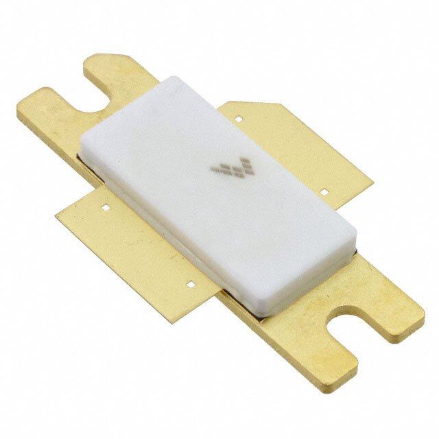
ICGOO电子元器件商城为您提供PD57060S-E由STMicroelectronics设计生产,在icgoo商城现货销售,并且可以通过原厂、代理商等渠道进行代购。 PD57060S-E价格参考¥499.79-¥511.22。STMicroelectronicsPD57060S-E封装/规格:晶体管 - FET,MOSFET - 射频, 射频 Mosfet LDMOS 28V 100mA 945MHz 14.3dB 60W PowerSO-10RF(直引线)。您可以下载PD57060S-E参考资料、Datasheet数据手册功能说明书,资料中有PD57060S-E 详细功能的应用电路图电压和使用方法及教程。
| 参数 | 数值 |
| 产品目录 | |
| 描述 | TRANS RF N-CH FET LDMOST PWRSO10 |
| 产品分类 | RF FET |
| 品牌 | STMicroelectronics |
| 数据手册 | |
| 产品图片 |
|
| 产品型号 | PD57060S-E |
| rohs | 无铅 / 符合限制有害物质指令(RoHS)规范要求 |
| 产品系列 | - |
| 产品目录页面 | |
| 供应商器件封装 | PowerSO-10RF(直引线) |
| 其它名称 | 497-5310-5 |
| 其它有关文件 | http://www.st.com/web/catalog/sense_power/FM1987/CL1989/SC1829/PF115440?referrer=70071840 |
| 功率-输出 | 60W |
| 包装 | 管件 |
| 噪声系数 | - |
| 增益 | 14.3dB |
| 封装/外壳 | PowerSO-10 裸露底部焊盘 |
| 晶体管类型 | LDMOS |
| 标准包装 | 50 |
| 电压-测试 | 28V |
| 电压-额定 | 65V |
| 电流-测试 | 100mA |
| 频率 | 945MHz |
| 额定电流 | 7A |
.jpg)


- 商务部:美国ITC正式对集成电路等产品启动337调查
- 曝三星4nm工艺存在良率问题 高通将骁龙8 Gen1或转产台积电
- 太阳诱电将投资9.5亿元在常州建新厂生产MLCC 预计2023年完工
- 英特尔发布欧洲新工厂建设计划 深化IDM 2.0 战略
- 台积电先进制程称霸业界 有大客户加持明年业绩稳了
- 达到5530亿美元!SIA预计今年全球半导体销售额将创下新高
- 英特尔拟将自动驾驶子公司Mobileye上市 估值或超500亿美元
- 三星加码芯片和SET,合并消费电子和移动部门,撤换高东真等 CEO
- 三星电子宣布重大人事变动 还合并消费电子和移动部门
- 海关总署:前11个月进口集成电路产品价值2.52万亿元 增长14.8%


PDF Datasheet 数据手册内容提取
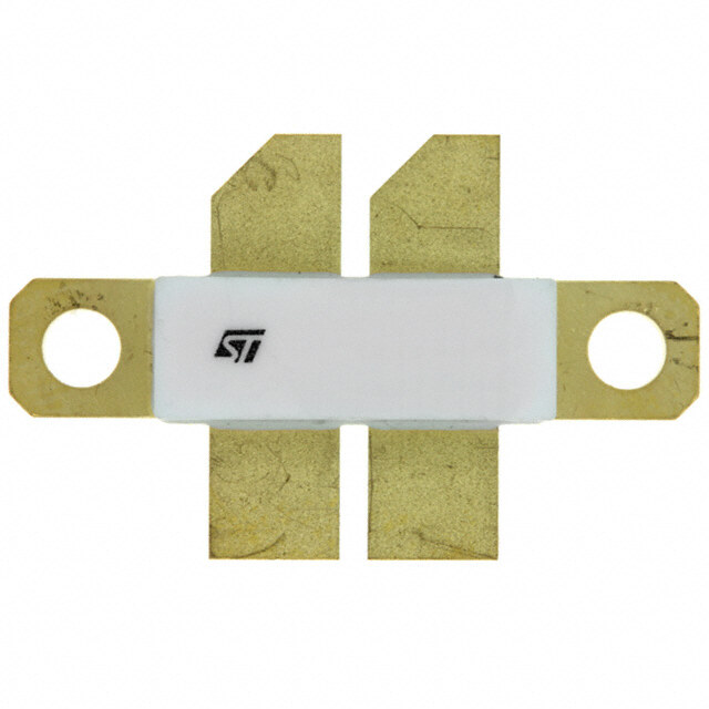
PD57060S-E RF POWER transistor, LdmoST plastic family N-channel enhancement-mode, lateral MOSFETs Features ■ Excellent thermal stability ■ Common source configuration ■ P = 60 W with 14.3dB gain@ 945 MHz/28 V OUT ■ New RF plastic package Description PowerSO-10RF (formed lead) The device is a common source N-channel, enhancement-mode lateral field-effect RF power MOSFET. It is designed for high gain, broad band commercial and industrial applications. It operates at 28 V in common source mode at frequencies up to 1 GHz. The device boasts the excellent gain, linearity and reliability of ST’s latest LDMOS technology mounted in the first true SMD plastic RF power package, PowerSO-10RF. PowerSO-10RF Device’s superior linearity performance makes it (straight lead) an ideal solution for base station applications. The PowerSO-10 plastic package, designed to offer high reliability, is the first ST JEDEC approved, high power SMD package. It has been Figure 1. Pin connection specially optmized for RF needs and offers Source excellent RF performances and ease of assembly. Mounting recommendations are available in www.st.com/rf/ (look for application note AN1294). Gate Drain Table 1. Device summary Order code Package Packing PD57060-E PowerSO-10RF (formed lead) Tube PD57060S-E PowerSO-10RF (straight lead) Tube PD57060TR-E PowerSO-10RF (formed lead) Tape and reel PD57060STR-E PowerSO-10RF (straight lead) Tape and reel June 2010 Doc ID 11758 Rev 4 1/21 www.st.com 21
Contents PD57060-E Contents 1 Electrical data . . . . . . . . . . . . . . . . . . . . . . . . . . . . . . . . . . . . . . . . . . . . . . 3 1.1 Maximum ratings . . . . . . . . . . . . . . . . . . . . . . . . . . . . . . . . . . . . . . . . . . . . 3 1.2 Thermal data . . . . . . . . . . . . . . . . . . . . . . . . . . . . . . . . . . . . . . . . . . . . . . . 3 2 Electrical characteristics . . . . . . . . . . . . . . . . . . . . . . . . . . . . . . . . . . . . . 4 2.1 Static . . . . . . . . . . . . . . . . . . . . . . . . . . . . . . . . . . . . . . . . . . . . . . . . . . . . . 4 2.2 Dynamic . . . . . . . . . . . . . . . . . . . . . . . . . . . . . . . . . . . . . . . . . . . . . . . . . . . 4 2.3 Moisture sensitivity level . . . . . . . . . . . . . . . . . . . . . . . . . . . . . . . . . . . . . . . 4 3 Impedances . . . . . . . . . . . . . . . . . . . . . . . . . . . . . . . . . . . . . . . . . . . . . . . . 5 4 Typical performance . . . . . . . . . . . . . . . . . . . . . . . . . . . . . . . . . . . . . . . . . 6 5 Test circuit . . . . . . . . . . . . . . . . . . . . . . . . . . . . . . . . . . . . . . . . . . . . . . . . . 9 6 Common source s-parameter . . . . . . . . . . . . . . . . . . . . . . . . . . . . . . . . 12 7 Package mechanical data . . . . . . . . . . . . . . . . . . . . . . . . . . . . . . . . . . . . 15 8 Revision history . . . . . . . . . . . . . . . . . . . . . . . . . . . . . . . . . . . . . . . . . . . 20 2/21 Doc ID 11758 Rev 4
PD57060-E Electrical data 1 Electrical data 1.1 Maximum ratings Table 2. Absolute maximum ratings (T = 25°C) CASE Symbol Parameter Value Unit V Drain-Source Voltage 65 V (BR)DSS V Gate-Source Voltage ± 20 V GS I Drain Current 7 A D P Power Dissipation (@ Tc = 70°C) 79 W DISS T Max. Operating Junction Temperature 165 °C J T Storage Temperature -65 to +150 °C STG 1.2 Thermal data Table 3. Thermal data Symbol Parameter Value Unit R Junction - case thermal resistance 1.0 °C/W thJC Doc ID 11758 Rev 4 3/21
Electrical characteristics PD57060-E 2 Electrical characteristics T = +25 oC CASE 2.1 Static Table 4. Static Symbol Test conditions Min Typ Max Unit V V = 0 I = 1 mA 65 V (BR)DSS GS DS I V = 0 V = 28 V 1 µA DSS GS DS I V = 20 V V = 0 V 1 µA GSS GS DS V V = 28 V I = 100 mA 2.0 4.0 V GS(Q) DS D V V = 10 V I = 3 A 0.7 0.8 V DS(ON) GS D G V = 10 V I = 3 A 2.5 mho FS DS D C V = 0 V = 28 V f = 1 MHz 83 pF ISS GS DS C V = 0 V = 28 V f = 1 MHz 58 pF OSS GS DS C V = 0 V = 28 V f = 1 MHz 3 pF RSS GS DS 2.2 Dynamic Table 5. Dynamic Symbol Test conditions Min Typ Max Unit POUT VDD = 28 V IDQ = 100 mA f = 945MHz 60 W GPS VDD = 28 V IDQ = 100 mA POUT = 60 W f = 945MHz 14.3 dB ηD VDD = 28 V IDQ = 100 mA POUT = 60 W f = 945MHz 54 % Load VDD = 28 V IDQ = 100 mA POUT = 60W f = 945MHz 5:1 VSWR Mismatch All Phase Angles 2.3 Moisture sensitivity level T able 6. Moisture sensitivity level Test methodology Rating J-STD-020B MSL 3 4/21 Doc ID 11758 Rev 4
PD57060-E Impedances 3 Impedances Figure 2. Current conventions Table 7. Impedance data Freq. (MHz) Z (Ω) Z (Ω) IN DL 890 MHz 0.646 + j 0.694 1.577 - j 0.997 925 MHz 0.568 + j 0.372 1.427 - j 1.459 945 MHz 0.705 + j 0.692 1.278 - j 1.935 960 MHz 0.591 + j 1.039 1.173 - j 2.464 Doc ID 11758 Rev 4 5/21
Typical performance PD57060-E 4 Typical performance Figure 3. Capacitance vs supply voltage Figure 4. Drain current vs gate source voltage C (pF) Id (A) 1000 8 7 6 100 Ciss 5 Coss 4 3 10 Crss 2 1 f = 1 MHz VDS=10 V 1 0 0 5 10 15 20 25 30 2 2.5 3 3.5 4 4.5 5 5.5 6 VDS (V) VGS (V) Figure 5. Gate-source voltage vs Figure 6. Output power vs input power case temperature VGS (Normalized) Pout (W) 1.06 80 945MHz 70 890MHz 1.04 925MHz 60 960MHz 1.02 Id = 5 A 50 1 Id = 4 A 40 Id = 3 A 0.98 Id = 2 A 30 0.96 Id = 1 A 20 Id = 0.5 A 0.94 10 VDS=28V VDS = 10 V IDQ=100mA 0.92 0 -25 0 25 50 75 100 0 0.5 1 1.5 2 2.5 3 3.5 4 Tc (°C) Pin (W) 6/21 Doc ID 11758 Rev 4
PD57060-E Typical performance Figure 7. Power gain vs output power Figure 8. Drain efficiency vs output power Gp (dB) Nd (%) 18 70 925MHz 16 890MHz 945MHz 925MHz 60 945MHz 14 960MHz 960MHz 12 50 890MHz 10 40 8 6 30 4 VDS=28V VDS=28V IDQ=100mA IDQ=100mA 2 20 0 10 20 30 40 50 60 70 80 0 10 20 30 40 50 60 70 80 Pout (W) Pout (W) Figure 9. Input return loss vs output power Figure 10. Output power vs bias current RL (dB) Pout (W) 0 80 925MHz 70 890MHz 890MHz -10 60 960MHz 960MHz 945MHz 50 925MHz -20 40 945MHz 30 -30 20 VDS=28V Pin=32.8dBm IDQ=100mA VDS=28V -40 10 0 10 20 30 40 50 60 70 80 0 0.5 1 1.5 2 2.5 Pout (W) IDQ (A) Doc ID 11758 Rev 4 7/21
Typical performance PD57060-E Figure 11. Drain efficiency vs bias current Figure 12. Output power vs supply voltage Nd (%) Pout (W) 70 70 945MHz 60 890MHz 945MHz 60 925MHz 890MHz 50 50 960MHz 960MHz 925MHz 40 40 30 30 20 20 Pin=32.8dBm Pin=32.8dBm IDQ=100mA VDS=28V 10 10 0 0.5 1 1.5 2 2.5 10 15 20 25 30 IDQ (A) VDS (V) Figure 13. Drain efficiency vs supply voltage Figure 14. Output power vs gate-source voltage Nd (%) Pout (W) 70 80 925MHz 890MHz 945MHz 70 60 890MHz 60 925MHz 9455MHz 50 960MHz 960MHz 50 40 40 30 30 20 Pin=32.8dBm 20 Pin=32.8dBm VDS=28v IDQ=100mA 10 10 10 15 20 25 30 0 1 2 3 4 5 VDS (V) VGS (V) 8/21 Doc ID 11758 Rev 4
PD57060-E Test circuit 5 Test circuit Figure 15. Test circuit schematic (cid:61)(cid:42)(cid:42)(cid:14) (cid:14)(cid:61)(cid:39)(cid:39) (cid:14) (cid:14) (cid:53)(cid:41) (cid:53)(cid:41) (cid:44)(cid:49) (cid:50)(cid:60)(cid:55) Note: 1 Dimensions at component symbols are reference for component placement. 2 Gap between ground & transmission line = 0.056 [1.42] +0.002 [0.05] -0.000 [0.00] typ. 3 Dimensions of input and output component from edge of transmission lines. Doc ID 11758 Rev 4 9/21
Test circuit PD57060-E Table 8. Test circuit component part list Component Description L1,L2 Inductor, 5 turns air wound #22AWG, ID 0.059{1.49}, nylon coated magnet WIRE FB1,FB2 Shield bead surface mount EMI R1 18 kΩ, 1 W surface mount chip resistor R2 4.7 MΩ, 1 W surface mount chip resistor R3 120 Ω, 2 W surface mount chip resistor C1,C2 3 pF ATC 100B surface mount ceramic chip capacitor C3,C10,C11 47 pF ATC 100B surface mount ceramic chip capacitor ,C15 C4,C9 0.8-8.0 pF giga trim variable capacitor C5,C6,C7,C 7.5 pF ATC 100B surface mount ceramic chip capacitor 8 C12 1000 pF ATC 700B surface mount ceramic chip capacitor C13,C17 0.1 µF, 500 V surface mount ceramic chip capacitor C14 10 µF, 50 V aluminum electrolytic radial lead capacitor C16 100 pF ATC 100B Surface mount ceramic chip capacitor C18 220 µF, 63 V aluminum electrolytic radial lead capacitor BOARD Roger, ultra lam 2000, THK 0.030”, εr = 2.55 2oz. ED Cu 2 sides. 10/21 Doc ID 11758 Rev 4
PD57060-E Test circuit Figure 16. Test circuit Figure 17. Test circuit photomaster s e h c n 4 i PD57060 6.4 inches Doc ID 11758 Rev 4 11/21
Common source s-parameter PD57060-E 6 Common source s-parameter Table 9. S-parameter for PD57060S-E (V = 28 V I = 1.5 A) DS DS Freq IS I S < Φ IS I S < Φ IS I S < Φ IS I S < Φ (MHz) 11 11 21 21 12 12 22 22 150 0.876 -168 7.35 63 0.011 -19 0.744 -165 200 0.892 -170 5.08 54 0.011 -23 0.785 -166 250 0.912 -172 3.74 46 0.007 -32 0.823 -167 300 0.927 -173 2.84 39 0.007 -30 0.856 -168 350 0.938 -174 2.23 33 0.006 -30 0.880 -170 400 0.948 -175 1.79 28 0.004 -38 0.903 -171 450 0.956 -176 1.47 24 0.003 -34 0.922 -172 500 0.961 -177 1.22 20 0.003 -12 0.931 -173 550 0.966 -178 1.03 17 0.003 -17 0.938 -174 600 0.968 -179 0.88 14 0.002 -8 0.942 -175 650 0.971 -180 0.76 11 0.002 45 0.945 -176 700 0.974 180 0.67 9 0.003 47 0.954 -177 750 0.975 179 0.59 6 0.003 47 0.960 -178 800 0.976 178 0.52 4 0.003 75 0.963 -179 850 0.977 178 0.47 2 0.004 71 0.968 -180 900 0.977 177 0.42 0 0.005 65 0.971 180 950 0.979 177 0.38 -2 0.005 68 0.970 179 1000 0.978 176 0.34 -4 0.005 80 0.974 179 1050 0.978 176 0.31 -5 0.007 76 0.969 178 1100 0.978 175 0.29 -7 0.007 77 0.972 178 1150 0.978 175 0.27 -8 0.007 78 0.971 177 1200 0.977 174 0.24 -10 0.008 80 0.973 176 1250 0.976 174 0.23 -11 0.008 77 0.974 176 1300 0.974 173 0.21 -13 0.009 74 0.971 175 1350 0.974 173 0.19 -14 0.009 76 0.969 175 1400 0.972 172 0.18 -16 0.009 81 0.970 174 1450 0.971 172 0.17 -16 0.010 86 0.968 174 1500 0.968 171 0.15 -17 0.010 91 0.967 173 12/21 Doc ID 11758 Rev 4
PD57060-E Common source s-parameter Table 10. S-parameter PD57060S-E (V = 28 V I = 150 mA) DS DS Freq IS I S < Φ IS I S < Φ IS I S < Φ IS I S < Φ (MHz) 11 11 21 21 12 12 22 22 150 0.881 -168 7.27 64 0.011 -20 0.744 -165 200 0.897 -170 5.03 54 0.009 -47 0.792 -166 250 0.915 -172 3.71 46 0.007 -32 0.823 -167 300 0.929 -173 2.82 39 0.007 -28 0.856 -168 350 0.939 -174 2.21 34 0.006 -30 0.879 -170 400 0.949 -175 1.78 29 0.004 -39 0.902 -171 450 0.956 -176 1.46 24 0.002 -30 0.920 -172 500 0.961 -177 1.21 20 0.003 -11 0.929 -173 550 0.966 -178 1.02 17 0.003 -16 0.937 -174 600 0.969 -179 0.87 14 0.001 -2 0.940 -175 650 0.972 -180 0.75 11 0.002 54 0.944 -176 700 0.974 180 0.66 8 0.003 47 0.953 -177 750 0.975 179 0.58 6 0.003 49 0.957 -178 800 0.976 178 0.51 4 0.003 78 0.962 -179 850 0.977 178 0.46 2 0.004 73 0.966 -180 900 0.977 177 0.41 0 0.005 64 0.969 180 950 0.979 177 0.37 -2 0.005 69 0.970 179 1000 0.978 176 0.34 -4 0.005 79 0.972 179 1050 0.979 175 0.31 -6 0.007 75 0.971 178 1100 0.978 175 0.28 -7 0.007 77 0.972 178 1150 0.977 175 0.26 -9 0.007 77 0.971 177 1200 0.977 174 0.24 -10 0.008 80 0.972 176 1250 0.975 174 0.22 -12 0.009 77 0.973 176 1300 0.974 173 0.20 -13 0.009 75 0.970 175 1350 0.974 173 0.19 -15 0.009 76 0.968 175 1400 0.972 172 0.18 -16 0.009 81 0.969 174 1450 0.971 172 0.16 -17 0.010 86 0.967 174 1500 0.969 171 0.15 -18 0.010 -89 0.968 173 Doc ID 11758 Rev 4 13/21
Common source s-parameter PD57060-E Table 11. S-parameter for PD57060S-E (V = 13.5 V I = 75 mA) DS DS Freq IS I S < Φ IS I S < Φ IS I S < Φ IS I S < Φ (MHz) 11 11 21 21 12 12 22 22 150 0.880 -173 4.67 69 0.012 -17 0.829 -174 200 0.891 -173 3.36 61 0.013 -33 0.848 -174 250 0.904 -175 2.54 55 0.010 -26 0.868 -175 300 0.915 -175 1.99 49 0.009 -20 0.881 -175 350 0.924 -176 1.61 43 0.009 -28 0.894 -176 400 0.933 -177 1.32 38 0.007 -36 0.909 -176 450 0.940 -177 1.10 34 0.005 -27 0.915 -177 500 0.946 -178 0.93 30 0.005 -24 0.926 -178 550 0.953 -179 0.80 27 0.005 -28 0.937 -178 600 0.956 -179 0.69 23 0.004 -24 0.942 -179 650 0.961 -180 0.61 20 0.003 -5 0.949 -180 700 0.964 179 0.53 18 0.004 10 0.954 180 750 0.966 179 0.48 15 0.003 4 0.955 179 800 0.967 178 0.43 13 0.002 43 0.960 178 850 0.968 178 0.38 11 0.004 51 0.956 178 900 0.971 177 0.35 9 0.004 43 0.962 177 950 0.971 177 0.32 7 0.004 55 0.966 176 1000 0.971 176 0.29 5 0.004 70 0.968 176 1050 0.975 175 0.26 4 0.006 68 0.971 175 1100 0.973 175 0.24 2 0.006 63 0.970 175 1150 0.974 175 0.22 0 0.006 67 0.971 174 1200 0.973 174 0.21 -1 0.006 74 0.972 174 1250 0.973 174 0.19 -3 0.007 73 0.969 174 1300 0.971 173 0.18 -4 0.008 70 0.967 173 1350 0.970 173 0.17 -5 0.008 77 0.967 172 1400 0.969 172 0.15 -6 0.009 82 0.965 172 1450 0.968 172 0.14 -6 0.010 84 0.966 171 1500 0.967 171 0.13 -7 0.010 89 0.967 171 14/21 Doc ID 11758 Rev 4
PD57060-E Package mechanical data 7 Package mechanical data In order to meet environmental requirements, ST offers these devices in different grades of ECOPACK® packages, depending on their level of environmental compliance. ECOPACK® specifications, grade definitions and product status are available at: www.st.com. ECOPACK® is an ST trademark. Doc ID 11758 Rev 4 15/21
Package mechanical data PD57060-E T able 12. PowerSO-10RF formed lead (gull wing) mechanical data Dim. mm. Inch Min. Typ. Max. Min. Typ. Max. A1 0 0.05 0.1 0. 0.0019 0.0038 A2 3.4 3.5 3.6 0.134 0.137 0.142 A3 1.2 1.3 1.4 0.046 0.05 0.054 A4 0.15 0.2 0.25 0.005 0.007 0.009 a 0.2 0.007 b 5.4 5.53 5.65 0.212 0.217 0.221 c 0.23 0.27 0.32 0.008 0.01 0.012 D 9.4 9.5 9.6 0.370 0.374 0.377 D1 7.4 7.5 7.6 0.290 0.295 0.298 E 13.85 14.1 14.35 0.544 0.555 0.565 E1 9.3 9.4 9.5 0.365 0.37 0.375 E2 7.3 7.4 7.5 0.286 0.292 0.294 E3 5.9 6.1 6.3 0.231 0.24 0.247 F 0.5 0.019 G 1.2 0.047 L 0.8 1 1.1 0.030 0.039 0.042 R1 0.25 0.01 R2 0.8 0.031 T 2 deg 5 deg 8 deg 2 deg 5 deg 8 deg T1 6 deg 6 deg T2 10 deg 10 deg Note: Resin protrusions not included (max value: 0.15 mm per side) Figure 18. Package dimensions for PowerSO-10RF formed lead (cid:41)(cid:79) (cid:44)(cid:45)(cid:35) (cid:53) (cid:50)(cid:17) (cid:52)(cid:18) (cid:52)(cid:17) (cid:39) (cid:45) (cid:37)(cid:18) (cid:37) (cid:38) (cid:37)(cid:17) (cid:37)(cid:19) (cid:44) (cid:50)(cid:18) (cid:50)(cid:17) (cid:33)(cid:20) (cid:36) (cid:51)(cid:69)(cid:69)(cid:0)(cid:68)(cid:69)(cid:84)(cid:65)(cid:73)(cid:76)(cid:0)(cid:43) (cid:36)(cid:69)(cid:84)(cid:65)(cid:73)(cid:76)(cid:0)(cid:43) (cid:52) (cid:51)(cid:67)(cid:65)(cid:76)(cid:69)(cid:0)(cid:17)(cid:21)(cid:14)(cid:16)(cid:16)(cid:16) (cid:51)(cid:69)(cid:69)(cid:0)(cid:68)(cid:69)(cid:84)(cid:65)(cid:73)(cid:76)(cid:0)(cid:43) (cid:44) (cid:39)(cid:65)(cid:85)(cid:71)(cid:69)(cid:0)(cid:80)(cid:76)(cid:65)(cid:78)(cid:69) (cid:52)(cid:18) (cid:50)(cid:17) (cid:35) (cid:16)(cid:14)(cid:19)(cid:21) (cid:33)(cid:19) (cid:33)(cid:17) (cid:33)(cid:18) Critical dimensions: - Stand-off (A1) (cid:52)(cid:17) (cid:36)(cid:17) (cid:50)(cid:17) - Overall width (L) (cid:36)(cid:69)(cid:84)(cid:65)(cid:73)(cid:76)(cid:0)(cid:43) (cid:51)(cid:67)(cid:65)(cid:76)(cid:69)(cid:0)(cid:17)(cid:21)(cid:14)(cid:16)(cid:16)(cid:16) 16/21 Doc ID 11758 Rev 4
PD57060-E Package mechanical data T able 13. PowerSO-10RF straight lead mechanical data Dim mm Inch Min Typ Max Min Typ Max A1 1.62 1.67 1.72 0.064 0.065 0.068 A2 3.4 3.5 3.6 0.134 0.137 0.142 A3 1.2 1.3 1.4 0.046 0.05 0.054 A4 0.15 0.2 0.25 0.005 0.007 0.009 a 0.2 0.007 b 5.4 5.53 5.65 0.212 0.217 0.221 c 0.23 0.27 0.32 0.008 0.01 0.012 D 9.4 9.5 9.6 0.370 0.374 0.377 D1 7.4 7.5 7.6 0.290 0.295 0.298 E 15.15 15.4 15.65 0.595 0.606 0.615 E1 9.3 9.4 9.5 0.365 0.37 0.375 E2 7.3 7.4 7.5 0.286 0.292 0.294 E3 5.9 6.1 6.3 0.231 0.24 0.247 F 0.5 0.019 G 1.2 0.047 R1 0.25 0.01 R2 0.8 0.031 T1 6 deg 6 deg T2 10 deg 10 deg Note: Resin protrusions not included (max value: 0.15 mm per side) Figure 19. Package dimensions for PowerSO-10RF straight lead (cid:41)(cid:79) (cid:44)(cid:45)(cid:35) (cid:53) (cid:33)(cid:17) (cid:50)(cid:17) (cid:52)(cid:18) (cid:52)(cid:17) (cid:39) (cid:45) (cid:37)(cid:18) (cid:37) (cid:38) (cid:37)(cid:17) (cid:37)(cid:19) (cid:44) (cid:35) (cid:33)(cid:20) (cid:50)(cid:18) (cid:50)(cid:17) (cid:36) (cid:52)(cid:18) (cid:50)(cid:17) (cid:33)(cid:19) (cid:33)(cid:18) CRITICAL DIMENSIONS: - Overall width (L) (cid:52)(cid:17) (cid:36)(cid:17) (cid:50)(cid:17) Doc ID 11758 Rev 4 17/21
Package mechanical data PD57060-E Figure 20. Tube information 18/21 Doc ID 11758 Rev 4
PD57060-E Package mechanical data Figure 21. Reel information Doc ID 11758 Rev 4 19/21
Revision history PD57060-E 8 Revision history Table 14. Document revision history Date Revision Changes 03-Nov-2005 1 First Issue. 13-Jul-2006 2 New template, added lead free info 23-Jan-2007 3 Update V in Table 4. GS(Q) 03-Jun-2010 4 Added: Table6: Moisture sensitivity level. 20/21 Doc ID 11758 Rev 4
PD57060-E Please Read Carefully: Information in this document is provided solely in connection with ST products. STMicroelectronics NV and its subsidiaries (“ST”) reserve the right to make changes, corrections, modifications or improvements, to this document, and the products and services described herein at any time, without notice. All ST products are sold pursuant to ST’s terms and conditions of sale. Purchasers are solely responsible for the choice, selection and use of the ST products and services described herein, and ST assumes no liability whatsoever relating to the choice, selection or use of the ST products and services described herein. No license, express or implied, by estoppel or otherwise, to any intellectual property rights is granted under this document. If any part of this document refers to any third party products or services it shall not be deemed a license grant by ST for the use of such third party products or services, or any intellectual property contained therein or considered as a warranty covering the use in any manner whatsoever of such third party products or services or any intellectual property contained therein. UNLESS OTHERWISE SET FORTH IN ST’S TERMS AND CONDITIONS OF SALE ST DISCLAIMS ANY EXPRESS OR IMPLIED WARRANTY WITH RESPECT TO THE USE AND/OR SALE OF ST PRODUCTS INCLUDING WITHOUT LIMITATION IMPLIED WARRANTIES OF MERCHANTABILITY, FITNESS FOR A PARTICULAR PURPOSE (AND THEIR EQUIVALENTS UNDER THE LAWS OF ANY JURISDICTION), OR INFRINGEMENT OF ANY PATENT, COPYRIGHT OR OTHER INTELLECTUAL PROPERTY RIGHT. UNLESS EXPRESSLY APPROVED IN WRITING BY AN AUTHORIZED ST REPRESENTATIVE, ST PRODUCTS ARE NOT RECOMMENDED, AUTHORIZED OR WARRANTED FOR USE IN MILITARY, AIR CRAFT, SPACE, LIFE SAVING, OR LIFE SUSTAINING APPLICATIONS, NOR IN PRODUCTS OR SYSTEMS WHERE FAILURE OR MALFUNCTION MAY RESULT IN PERSONAL INJURY, DEATH, OR SEVERE PROPERTY OR ENVIRONMENTAL DAMAGE. ST PRODUCTS WHICH ARE NOT SPECIFIED AS "AUTOMOTIVE GRADE" MAY ONLY BE USED IN AUTOMOTIVE APPLICATIONS AT USER’S OWN RISK. Resale of ST products with provisions different from the statements and/or technical features set forth in this document shall immediately void any warranty granted by ST for the ST product or service described herein and shall not create or extend in any manner whatsoever, any liability of ST. ST and the ST logo are trademarks or registered trademarks of ST in various countries. Information in this document supersedes and replaces all information previously supplied. The ST logo is a registered trademark of STMicroelectronics. All other names are the property of their respective owners. © 2010 STMicroelectronics - All rights reserved STMicroelectronics group of companies Australia - Belgium - Brazil - Canada - China - Czech Republic - Finland - France - Germany - Hong Kong - India - Israel - Italy - Japan - Malaysia - Malta - Morocco - Philippines - Singapore - Spain - Sweden - Switzerland - United Kingdom - United States of America www.st.com Doc ID 11758 Rev 4 21/21
Mouser Electronics Authorized Distributor Click to View Pricing, Inventory, Delivery & Lifecycle Information: S TMicroelectronics: PD57060STR-E PD57060TR-E PD57060-E PD57060S-E