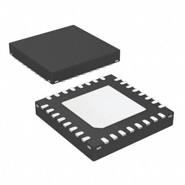
ICGOO在线商城 > PCF8575CDGVR
- 型号: PCF8575CDGVR
- 制造商: Texas Instruments
- 库位|库存: xxxx|xxxx
- 要求:
| 数量阶梯 | 香港交货 | 国内含税 |
| +xxxx | $xxxx | ¥xxxx |
查看当月历史价格
查看今年历史价格
PCF8575CDGVR产品简介:
ICGOO电子元器件商城为您提供PCF8575CDGVR由Texas Instruments设计生产,在icgoo商城现货销售,并且可以通过原厂、代理商等渠道进行代购。 提供PCF8575CDGVR价格参考以及Texas InstrumentsPCF8575CDGVR封装/规格参数等产品信息。 你可以下载PCF8575CDGVR参考资料、Datasheet数据手册功能说明书, 资料中有PCF8575CDGVR详细功能的应用电路图电压和使用方法及教程。
| 参数 | 数值 |
| 产品目录 | 集成电路 (IC)半导体 |
| 描述 | IC I/O EXPANDER I2C 16B 24TVSOP接口-I/O扩展器 Remote 16-Bit I2C & SMBus I/O Expander |
| 产品分类 | |
| I/O数 | 16 |
| 品牌 | Texas Instruments |
| 产品手册 | |
| 产品图片 |
|
| rohs | 符合RoHS无铅 / 符合限制有害物质指令(RoHS)规范要求 |
| 产品系列 | 接口 IC,接口-I/O扩展器,Texas Instruments PCF8575CDGVR- |
| 数据手册 | |
| 产品型号 | PCF8575CDGVR |
| 中断输出 | 是 |
| 产品培训模块 | http://www.digikey.cn/PTM/IndividualPTM.page?site=cn&lang=zhs&ptm=8660 |
| 产品目录页面 | |
| 产品种类 | 接口-I/O扩展器 |
| 供应商器件封装 | 24-TVSOP |
| 其它名称 | 296-17914-1 |
| 制造商产品页 | http://www.ti.com/general/docs/suppproductinfo.tsp?distId=10&orderablePartNumber=PCF8575CDGVR |
| 包装 | 剪切带 (CT) |
| 单位重量 | 61 mg |
| 商标 | Texas Instruments |
| 安装类型 | 表面贴装 |
| 安装风格 | SMD/SMT |
| 封装 | Reel |
| 封装/外壳 | 24-TFSOP(0.173",4.40mm 宽) |
| 封装/箱体 | TVSOP-24 |
| 工作温度 | -40°C ~ 85°C |
| 工作温度范围 | - 40 C to + 85 C |
| 工作电源电压 | 4.5 V to 5.5 V |
| 工厂包装数量 | 2000 |
| 接口 | I²C, SMBus |
| 最大工作频率 | 400 kHz |
| 标准包装 | 1 |
| 特性 | POR |
| 电压-电源 | 4.5 V ~ 5.5 V |
| 电流-灌/拉输出 | 10mA, 25mA |
| 系列 | PCF8575C |
| 输入/输出端数量 | 16 I/O |
| 输出类型 | 开路漏极 |
| 逻辑系列 | PCF8575C |
| 频率-时钟 | 400kHz |


PDF Datasheet 数据手册内容提取
Product Sample & Technical Tools & Support & Folder Buy Documents Software Community PCF8575C SCPS123F–MARCH2005–REVISEDJANUARY2015 2 PCF8575C Remote 16-Bit I C AND SMBus Low-Power I/O Expander with Interrupt Output 1 Features 3 Description • I2CtoParallel-PortExpander This 16-bit I/O expander for the two-line bidirectional 1 bus (I2C) is designed for 4.5-V to 5.5-V V • Open-DrainInterruptOutput CC operation. • LowStandby-CurrentConsumptionof The PCF8575C provides general-purpose remote I/O 10μAMaximum expansionformostmicrocontrollerfamiliesviatheI2C • CompatibleWithMostMicrocontrollers interfaceserialclock(SCL)andserialdata(SDA). • 400-kHzFastI2CBus The device features a 16-bit quasi-bidirectional • AddressbyThreeHardwareAddressPinsforUse input/output (I/O) port (P07–P00, P17–P10), including ofuptoEightDevices latched outputs with high-current drive capability for • LatchedOutputsWithHigh-CurrentDrive directly driving LEDs. Each quasi-bidirectional I/O can CapabilityforDirectlyDrivingLEDs be used as an input or output without the use of a data-direction control signal. At power on, the I/Os • Latch-UpPerformanceExceeds100mAPer are in 3-state mode. The strong pullup to V allows JESD78,ClassII CC fast-rising edges into heavily loaded outputs. This • ESDProtectionExceedsJESD22 device turns on when an output is written high and is – 2000-VHuman-BodyModel switched off by the negative edge of SCL. The I/Os should be high before being used as inputs. After – 200-VMachineModel poweron,asalltheI/Osaresetto3-state,allofthem – 1000-VCharged-DeviceModel can be used as inputs. Any change in setting of the I/Os as either inputs or outputs can be done with the 2 Applications write mode. If a high is applied externally to an I/O that has been written earlier to low, a large current • TelecomShelters:FilterUnits (I )flowstoGND. OL • Servers • Routers(TelecomSwitchingEquipment) DeviceInformation(1) • PersonalComputers PARTNUMBER PACKAGE(PIN) BODYSIZE • PersonalElectronics SSOP(24) 8.20mm×5.30mm • IndustrialAutomation QSOP(24) 8.65mm×3.90 TVSOP(24) 5.00mm×4.50mm • ProductswithGPIO-LimitedProcessors PCF8575C SOIC(24) 15.40mm×7.50mm TSSOP(24) 7.80mm×4.40mm QFN(24) 4.0mm×4.0mm (1) For all available packages, see the orderable addendum at theendofthedatasheet. VCC SDA I2C or SMBus Master SCL P00 (e.g. Processor) INT P01 Peripheral Devices P02 RESET,ENABLE, P03 or control inputs P04 INTor status A0 P05 outputs A1 P06 LEDs A2 P07 GND PCF8575C P10 P11 Peripheral Devices P12 RESET,ENABLE, P13 or control inputs P14 INTor status P15 outputs P16 LEDs P17 1 An IMPORTANT NOTICE at the end of this data sheet addresses availability, warranty, changes, use in safety-critical applications, intellectualpropertymattersandotherimportantdisclaimers.PRODUCTIONDATA.
PCF8575C SCPS123F–MARCH2005–REVISEDJANUARY2015 www.ti.com Table of Contents 1 Features.................................................................. 1 8.2 FunctionalBlockDiagram.......................................12 2 Applications........................................................... 1 8.3 FeatureDescription.................................................13 3 Description............................................................. 1 8.4 DeviceFunctionalModes........................................15 4 RevisionHistory..................................................... 2 9 ApplicationandImplementation........................ 17 9.1 ApplicationInformation............................................17 5 PinConfiguration................................................... 3 9.2 TypicalApplication .................................................17 6 Specifications......................................................... 4 10 PowerSupplyRecommendations..................... 20 6.1 AbsoluteMaximumRatings.....................................4 10.1 Power-OnResetRequirements ...........................20 6.2 ESDRatings..............................................................4 11 Layout................................................................... 22 6.3 RecommendedOperatingConditions......................4 6.4 ThermalInformation..................................................4 11.1 LayoutGuidelines.................................................22 6.5 ElectricalCharacteristics..........................................5 11.2 LayoutExample....................................................23 6.6 I2CInterfaceTimingRequirements..........................5 12 DeviceandDocumentationSupport................. 24 6.7 SwitchingCharacteristics.........................................6 12.1 Trademarks...........................................................24 6.8 TypicalCharacteristics..............................................6 12.2 ElectrostaticDischargeCaution............................24 7 ParameterMeasurementInformation..................8 12.3 Glossary................................................................24 8 DetailedDescription............................................ 11 13 Mechanical,Packaging,andOrderable Information........................................................... 24 8.1 Overview.................................................................11 4 Revision History ChangesfromRevisionE(October2007)toRevisionF Page • AddedApplications,DeviceInformationtable,PinFunctionstable,ESDRatingstable,ThermalInformationtable, TypicalCharacteristics,FeatureDescriptionsection,DeviceFunctionalModes,ApplicationandImplementation section,PowerSupplyRecommendationssection,Layoutsection,DeviceandDocumentationSupportsection,and Mechanical,Packaging,andOrderableInformationsection.................................................................................................. 1 • DeletedOrderingInformationtable........................................................................................................................................ 1 2 SubmitDocumentationFeedback Copyright©2005–2015,TexasInstrumentsIncorporated ProductFolderLinks:PCF8575C
PCF8575C www.ti.com SCPS123F–MARCH2005–REVISEDJANUARY2015 5 Pin Configuration DB, DBQ, DGV, DW, OR PW PACKAGE RGE PACKAGE (TOPVIEW) (TOPVIEW) INT 1 24 VCC A2 A1INTVCCSDA SCL A1 2 23 SDA 24 23 22 21 20 19 A2 3 22 SCL P00 1 18 A0 P00 4 21 A0 P01 2 17 P17 P01 5 20 P17 P03 3 16 P16 P02 6 19 P16 P03 4 15 P15 P03 7 18 P15 P04 5 14 P14 P04 8 17 P14 P05 6 13 P13 P05 9 16 P13 7 8 9 10 11 12 P06 10 15 P12 6 7 D0 1 2 P07 11 14 P11 P0 P0 GNP1 P1 P1 GND 12 13 P10 PinFunctions PIN TYPE NAME NO. DESCRIPTION DB,DBQ,DGV, RGE DW,ANDPW INT 1 22 I Interruptoutput.ConnecttoVCCthroughapullupresistor. A1 2 23 I Addressinput1.ConnectdirectlytoVCCorground.Pullupresistorsarenotneeded. A2 3 24 I Addressinput2.ConnectdirectlytoVCCorground.Pullupresistorsarenotneeded. P00 4 1 I/O P-portinput/output.Open-draindesignstructure.ConnecttoVCCthroughapullupresistor. P01 5 2 I/O P-portinput/output.Open-draindesignstructure.ConnecttoVCCthroughapullupresistor. P02 6 3 I/O P-portinput/output.Open-draindesignstructure.ConnecttoVCCthroughapullupresistor. P03 7 4 I/O P-portinput/output.Open-draindesignstructure.ConnecttoVCCthroughapullupresistor. P04 8 5 I/O P-portinput/output.Open-draindesignstructure.ConnecttoVCCthroughapullupresistor. P05 9 6 I/O P-portinput/output.Open-draindesignstructure.ConnecttoVCCthroughapullupresistor. P06 10 7 I/O P-portinput/output.Open-draindesignstructure.ConnecttoVCCthroughapullupresistor. P07 11 8 I/O P-portinput/output.Open-draindesignstructure.ConnecttoVCCthroughapullupresistor. GND 12 9 — Ground P10 13 10 I/O P-portinput/output.Open-draindesignstructure.ConnecttoVCCthroughapullupresistor. P11 14 11 I/O P-portinput/output.Open-draindesignstructure.ConnecttoVCCthroughapullupresistor. P12 15 12 I/O P-portinput/output.Open-draindesignstructure.ConnecttoVCCthroughapullupresistor. P13 16 13 I/O P-portinput/output.Open-draindesignstructure.ConnecttoVCCthroughapullupresistor. P14 17 14 I/O P-portinput/output.Open-draindesignstructure.ConnecttoVCCthroughapullupresistor. P15 18 15 I/O P-portinput/output.Open-draindesignstructure.ConnecttoVCCthroughapullupresistor. P16 19 16 I/O P-portinput/output.Open-draindesignstructure.ConnecttoVCCthroughapullupresistor. P17 20 17 I/O P-portinput/output.Open-draindesignstructure.ConnecttoVCCthroughapullupresistor. A0 21 18 I Addressinput0.ConnectdirectlytoVCCorground.Pullupresistorsarenotneeded. SCL 22 19 I Serialclockline.ConnecttoVCCthroughapullupresistor SDA 23 20 I/O Serialdataline.ConnecttoVCCthroughapullupresistor. VCC 24 21 — Supplyvoltage Copyright©2005–2015,TexasInstrumentsIncorporated SubmitDocumentationFeedback 3 ProductFolderLinks:PCF8575C
PCF8575C SCPS123F–MARCH2005–REVISEDJANUARY2015 www.ti.com 6 Specifications 6.1 Absolute Maximum Ratings overoperatingfree-airtemperaturerange(unlessotherwisenoted)(1) MIN MAX UNIT V Supplyvoltagerange –0.5 6.5 V CC V Inputvoltagerange(2) –0.5 V +0.5 V I CC V Outputvoltagerange(2) –0.5 V +0.5 V O CC I Inputclampcurrent V <0 –20 mA IK I I Outputclampcurrent V <0 –20 mA OK O I Input/outputclampcurrent V <0orV >V ±400 μA OK O O CC I Continuousoutputlowcurrent V =0toV 50 mA OL O CC I Continuousoutputhighcurrent V =0toV –4 mA OH O CC ContinuouscurrentthroughV orGND ±100 mA CC T Storagetemperaturerange –65 150 °C stg (1) StressesbeyondthoselistedunderAbsoluteMaximumRatingsmaycausepermanentdamagetothedevice.Thesearestressratings only,andfunctionaloperationofthedeviceattheseoranyotherconditionsbeyondthoseindicatedunderRecommendedOperating Conditionsisnotimplied.Exposuretoabsolute-maximum-ratedconditionsforextendedperiodsmayaffectdevicereliability. (2) Theinputnegative-voltageandoutputvoltageratingsmaybeexceedediftheinputandoutputcurrentratingsareobserved. 6.2 ESD Ratings VALUE UNIT Humanbodymodel(HBM),perANSI/ESDA/JEDECJS-001,allpins 2000 V(ESD) Electrostaticdischarge Chargeddevicemodel(CDM),perJEDECspecificationJESD22- V 1000 C101,allpins 6.3 Recommended Operating Conditions MIN MAX UNIT V Supplyvoltage 4.5 5.5 V CC A0,A1,A2,SDA,andSCL 0.7×V V +0.5 CC CC V High-levelinputvoltage V IH P07–P00andP17–P10 0.8×V V +0.5 CC CC A0,A1,A2,SDA,andSCL –0.5 0.3×V CC V Low-levelinputvoltage V IL P07–P00andP17–P10 –0.5 0.6×V CC I P-porttransientpullupcurrent –10 mA OHT I P-portlow-leveloutputcurrent 25 mA OL T Operatingfree-airtemperature –40 85 °C A 6.4 Thermal Information PCF8575 THERMALMETRIC(1) DB DBQ DGV DW PW RGE UNIT 24PINS R Junction-to-ambientthermalresistance 63 61 86 46 88 53 °C/W θJA (1) Formoreinformationabouttraditionalandnewthermalmetrics,seetheICPackageThermalMetricsapplicationreport(SPRA953). 4 SubmitDocumentationFeedback Copyright©2005–2015,TexasInstrumentsIncorporated ProductFolderLinks:PCF8575C
PCF8575C www.ti.com SCPS123F–MARCH2005–REVISEDJANUARY2015 6.5 Electrical Characteristics overrecommendedoperatingfree-airtemperaturerange(unlessotherwisenoted) PARAMETER TESTCONDITIONS V MIN TYP(1) MAX UNIT CC 4.5Vto V Inputdiodeclampvoltage I =–18mA –1.2 V IK I 5.5V V Power-onresetvoltage(2) V =V orGND, I =0 V 1.2 1.8 V POR I CC O POR I P-porttransientpullupcurrent HighduringACKV =GND 4.5V –0.5 –1 mA OHT OH 4.5Vto SDA V =0.4V 3 OL 5.5V VOL=0.4V 4.5Vto 5 15 I Pport mA OL V =1V 5.5V 10 25 OL 4.5Vto INT V =0.4V 1.6 OL 5.5V SCL,SDA 4.5Vto ±2 I V =V orGND μA I A0,A1,A2 I CC 5.5V ±1 4.5Vto I Pport V ≥V orV ≤GND ±400 μA IHL I CC I 5.5V Operatingmode V =V orGND, I =0,f =400kHz 100 200 I CC O SCL I 5.5V μA CC Standbymode V =V orGND, I =0,f =0kHz 2.5 10 I CC O SCL OneinputatV –0.6V, 4.5Vto ΔI Supplycurrentincrease CC 200 μA CC OtherinputsatV orGND 5.5V CC 4.5Vto C SCL V =V orGND 3 7 pF i I CC 5.5V SDA 4.5Vto 3 7 C V =V orGND pF io Pport IO CC 5.5V 4 10 (1) AlltypicalvaluesareatV =5V,T =25°C. CC A (2) Thepower-onresetcircuitresetstheI2CbuslogicwithV <V andsetsallI/Ostologichigh(withcurrentsourcetoV ). CC POR CC 6.6 I2C Interface Timing Requirements overrecommendedoperatingfree-airtemperaturerange(unlessotherwisenoted)(seeFigure7) MIN MAX UNIT f I2Cclockfrequency 400 kHz scl t I2Cclockhightime 0.6 μs sch t I2Cclocklowtime 1.3 μs scl t I2Cspiketime 50 ns sp t I2Cserial-datasetuptime 100 ns sds t I2Cserial-dataholdtime 0 ns sdh t I2Cinputrisetime 20+0.1C (1) 300 ns icr b t I2Cinputfalltime 20+0.1C (1) 300 ns icf b t I2Coutputfalltime(10-pFto400-pFbus) 300 ns ocf t I2Cbusfreetimebetweenstopandstart 1.3 μs buf t I2Cstartorrepeatedstartconditionsetup 0.6 μs sts t I2Cstartorrepeatedstartconditionhold 0.6 μs sth t I2Cstopconditionsetup 0.6 μs sps t Valid-datatime SCLlowtoSDAoutputvalid 1.2 μs vd C I2Cbuscapacitiveload 400 pF b (1) C =totalbuscapacitanceofonebuslineinpF b Copyright©2005–2015,TexasInstrumentsIncorporated SubmitDocumentationFeedback 5 ProductFolderLinks:PCF8575C
PCF8575C SCPS123F–MARCH2005–REVISEDJANUARY2015 www.ti.com 6.7 Switching Characteristics overrecommendedoperatingfree-airtemperaturerange,C ≤100pF(unlessotherwisenoted)(seeFigure8andFigure9) L FROM TO PARAMETER MIN MAX UNIT (INPUT) (OUTPUT) t Interruptvalidtime Pport INT 4 μs iv t Interruptresetdelaytime SCL INT 4 μs ir t Outputdatavalid SCL Pport 4 μs pv t Inputdatasetuptime Pport SCL 0 μs su t Inputdataholdtime Pport SCL 4 μs h 6.8 Typical Characteristics T =25°C(unlessotherwisenoted) A 100 9 fSCL= 400 kHz SCL= VCC 90 AllI/Osunloaded 8 AllI/Osunloaded A) 7800 VCC= 5 V A) 7 m m 6 urrent ( 5600 urrent ( 5 VCC= 5 V C C 4 y 40 y uppl 30 uppl 3 S S 20 2 10 1 0 0 −50 −25 0 25 50 75 100 125 −50 −25 0 25 50 75 100 125 Temperature(°C) Temperature (°C) Figure1.SupplyCurrentvsTemperature Figure2.StandbySupplyCurrentvsTemperature 100 35 fSCL= 400 kHz VCC= 5 V 90 AllI/Osunloaded 30 TA=−40ºC 80 mA) 70 A) 25 TA= 25ºC y Current ( 456000 I(mSINK 1250 pl up 30 10 S TA= 85ºC 20 5 10 0 0 2.0 2.5 3.0 3.5 4.0 4.5 5.0 5.5 0.0 0.1 0.2 0.3 0.4 0.5 0.6 SupplyVoltage(V) VOL(V) Figure3.SupplyCurrentvsSupplyVoltage Figure4.I/OSinkCurrentvsOutputLowVoltage 6 SubmitDocumentationFeedback Copyright©2005–2015,TexasInstrumentsIncorporated ProductFolderLinks:PCF8575C
PCF8575C www.ti.com SCPS123F–MARCH2005–REVISEDJANUARY2015 Typical Characteristics (continued) T =25°C(unlessotherwisenoted) A 400 500 350 VCC= 5 V,ISINK=10mA 400 300 V) ( H V)250 VO 300 m − (200 C L C O V V 200 150 100 VCC= 5 V,ISINK= 1mA 100 50 VCC= 5 V, ISOURCE= 10 mA 0 0 −50 −25 0 25 50 75 100 125 −50 −25 0 25 50 75 100 125 Temperature (°C) Temperature (°C) Figure5.I/OOutputLowVoltagevsTemperature Figure6.I/OHighVoltagevsTemperature Copyright©2005–2015,TexasInstrumentsIncorporated SubmitDocumentationFeedback 7 ProductFolderLinks:PCF8575C
PCF8575C SCPS123F–MARCH2005–REVISEDJANUARY2015 www.ti.com 7 Parameter Measurement Information VCC RL= 1 kW SDA DUT CL= 50 pF SDALOAD CONFIGURATION 3 Bytes for Complete Device Programming Stop Start Address R/W Data Data Stop Address Address ACK Condition Condition Bit 7 Bit 0 Bit 07 Bit 10 Condition Bit 6 Bit 1 (A) (P) (S) (MSB) (LSB) (MSB) (LSB) (P) tscl tsch 0.7×VCC SCL 0.3×VCC ticr tPHL tsts tbuf ticf tsp tPLH SDA 0.7×VCC 0.3×VCC ticf ticr tsdh tsps tsth tsds Repeat Start Stop Start or Condition Condition Repeat Start Condition VOLTAGE WAVEFORMS BYTE DESCRIPTION 1 I2C address 2, 3 P-port data Figure7. I2CInterfaceLoadCircuitandVoltageWaveforms 8 SubmitDocumentationFeedback Copyright©2005–2015,TexasInstrumentsIncorporated ProductFolderLinks:PCF8575C
PCF8575C www.ti.com SCPS123F–MARCH2005–REVISEDJANUARY2015 Parameter Measurement Information (continued) VCC RL= 4.7 kΩ INT DUT CL= 100 pF INTERRUPT LOAD CONFIGURATION ACK From Slave Start ACK Condition 16 Bits From Slave R/W (2 Data Bytes) SlaveAddress (PCF8575) From Port Data From Port S 0 1 0 0 A2 A1 A0 1 A Data 1 Data 2 A Data 3 1 P 1 2 3 4 5 6 7 8 A A tir B tir B INT A tiv tsps A Data Into Address Data 1 Data 2 Data 3 Port INT 00..73××VVCCCC SCL R/W A 00..73××VVCCCC tiv tir Pn 00..37××VVCCCC INT 00..73××VVCCCC ViewA−A View B−B Figure8. InterruptLoadCircuitandVoltageWaveforms Copyright©2005–2015,TexasInstrumentsIncorporated SubmitDocumentationFeedback 9 ProductFolderLinks:PCF8575C
PCF8575C SCPS123F–MARCH2005–REVISEDJANUARY2015 www.ti.com Parameter Measurement Information (continued) VCC VCC RL= 1 kΩ RL= 4.7 kΩ SDA INT Pn DUT DUT DUT CL= 50 pF CL= 100 pF CL= 100 pF GND GND GND SDALOAD CONFIGURATION INTERRUPT LOAD CONFIGURATION P-PORT LOAD CONFIGURATION SCL 0.7×VCC P00 A P17 0.3×VCC Slave ACK SDA tpv Pn Last Stable Bit Unstable Data Write-Mode Timing (R/W= 0) SCL 0.7×VCC P00 A P17 0.3×VCC tsu th 0.7×VCC Pn 0.3×VCC Read-Mode Timing (R/W= 1) Figure9. P-PortLoadCircuitsandVoltageWaveforms 10 SubmitDocumentationFeedback Copyright©2005–2015,TexasInstrumentsIncorporated ProductFolderLinks:PCF8575C
PCF8575C www.ti.com SCPS123F–MARCH2005–REVISEDJANUARY2015 8 Detailed Description 8.1 Overview The PCF8575C provides an open-drain interrupt (INT) output, which can be connected to the interrupt input of a microcontroller. An interrupt is generated by any rising or falling edge of the port inputs in the input mode. After time (t ), the signal INT is valid. Resetting and reactivating the interrupt circuit is achieved when data on the port iv ischangedtotheoriginalsetting,ordataisreadfromorwrittentotheportthatgeneratedtheinterrupt.Resetting occurs in the read mode at the acknowledge (ACK) bit after the rising edge of the SCL signal or in the write modeattheACKbitafterthefallingedgeoftheSCLsignal.InterruptsthatoccurduringtheACKclockpulsecan be lost (or be very short), due to the resetting of the interrupt during this pulse. Each change of the I/Os after resetting is detected and is transmitted as INT. Reading from or writing to another device does not affect the interruptcircuit. By sending an interrupt signal on this line, the remote I/O can inform the microcontroller if there is incoming data on its ports, without having to communicate via the I2C bus. Thus, the PCF8575C can remain a simple slave device. Every data transmission to or from the PCF8575C must consist of an even number of bytes. The first data byte in every pair refers to port 0 (P07–P00), and the second data byte in every pair refers to port 1 (P17–P10). To write to the ports (output mode), the master first addresses the slave device, setting the last bit of the byte containing the slave address to logic 0. The PCF8575C acknowledges and the master sends the first data byte for P07–P00. After the first data byte is acknowledged by the PCF8575C, the second data byte (P17–P10) is sentbythemaster.Onceagain,thePCF8575Cacknowledgesthereceiptofthedata,afterwhichthis16-bitdata ispresentedontheportlines. The number of data bytes that can be sent successively is not limited. After every two bytes, the previous data is overwritten. When the PCF8575C receives the pairs of data bytes, the first byte is referred to as P07–P00 and thesecondbyteasP17–P10.ThethirdbyteisreferredtoasP07–P00,thefourthbyteasP17–P10,andsoon. Before reading from the PCF8575C, all ports desired as input should be set to logic 1. To read from the ports (input mode), the master first addresses the slave device, setting the last bit of the byte containing the slave addresstologic1.ThedatabytesthatfollowontheSDAarethevaluesontheports.Ifthedataontheinputport changesfasterthanthemastercanread,thisdatamaybelost. When power is applied to V , an internal power-on reset holds the PCF8575C in a reset state until V has CC CC reached V . At that time, the reset condition is released, and the device I2C-bus state machine initializes the POR bustoitsdefaultstate. The hardware pins (A0, A1, and A2) are used to program and vary the fixed I2C address, and allow up to eight devices to share the same I2C bus or SMBus. The fixed I2C address of the PCF8575C is the same as the PCF8575, PCF8574, PCA9535, and PCA9555, allowing up to eight of these devices, in any combination, to sharethesameI2CbusorSMBus. Copyright©2005–2015,TexasInstrumentsIncorporated SubmitDocumentationFeedback 11 ProductFolderLinks:PCF8575C
PCF8575C SCPS123F–MARCH2005–REVISEDJANUARY2015 www.ti.com 8.2 Functional Block Diagram 8.2.1 SimplifiedBlockDiagramofDevice PCF8575C 1 Interrupt INT LPFilter Logic 21 A0 2 A1 P07−P00 3 A2 22 SCL Input I2C Bus Shift I/O 23 Filter Control 16 Bits SDA Register Port P17−P10 Write Pulse 24 Read Pulse VCC Power-On GND 12 Reset 8.2.2 SimplifiedSchematicDiagramofEachP-PortInput/Output Write Pulse VCC IOHT Data From D Q Shift Register FF P07−P00 CI P17−P10 S IOL Power-On Reset D Q GND FF CI Read Pulse S To Interrupt Data To Logic Shift Register 12 SubmitDocumentationFeedback Copyright©2005–2015,TexasInstrumentsIncorporated ProductFolderLinks:PCF8575C
PCF8575C www.ti.com SCPS123F–MARCH2005–REVISEDJANUARY2015 8.3 Feature Description 8.3.1 I2CInterface The bidirectional I2C bus consists of the serial clock (SCL) and serial data (SDA) lines. Both lines must be connected to a positive supply via a pullup resistor when connected to the output stages of a device. Data transfermaybeinitiatedonlywhenthebusisnotbusy. I2C communication with this device is initiated by a master sending a start condition, a high-to-low transition on the SDA input/output while the SCL input is high (see Figure 10). After the start condition, the device address byte is sent, MSB first, including the data direction bit (R/W). This device does not respond to the general call address. After receiving the valid address byte, this device responds with an ACK, a low on the SDA input/output during the high of the ACK-related clock pulse. The address inputs (A2–A0) of the slave device must not be changedbetweenthestartandthestopconditions. The data byte follows the address ACK. If the R/W bit is high, the data from this device are the values read from thePport.IftheR/Wbitislow,thedataarefromthemaster,tobeoutputtothePport.Thedatabyteisfollowed by an ACK sent from this device. If other data bytes are sent from the master, following the ACK, they are ignoredbythisdevice.Dataareoutputonlyifcompletebytesarereceivedandacknowledged.Theoutputdatais validattime(t )afterthelow-to-hightransitionofSCL,duringtheclockcyclefortheACK. pv On the I2C bus, only one data bit is transferred during each clock pulse. The data on the SDA line must remain stable during the high pulse of the clock period, as changes in the data line at this time are interpreted as control commands(startorstop)(seeFigure11). A stop condition, a low-to-high transition on the SDA input/output while the SCL input is high, is sent by the master(seeFigure10). Thenumberofdatabytestransferredbetweenthestartandthestopconditionsfromtransmittertoreceiverisnot limited. Each byte of eight bits is followed by one ACK bit. The transmitter must release the SDA line before the receivercansendanACKbit. A slave receiver that is addressed must generate an ACK after the reception of each byte. Also, a master must generate an ACK after the reception of each byte that has been clocked out of the slave transmitter. The device that acknowledges has to pull down the SDA line during the ACK clock pulse so that the SDA line is stable low during the high pulse of the ACK-related clock period (see Figure 12). Setup and hold times must be taken into account. A master receiver must signal an end of data to the transmitter by not generating an acknowledge (NACK) after the last byte that has been clocked out of the slave. This is done by the master receiver by holding the SDA line high.Inthisevent,thetransmittermustreleasethedatalinetoenablethemastertogenerateastopcondition. SDA SCL S P Start Condition Stop Condition Figure10. DefinitionofStartandStopConditions Copyright©2005–2015,TexasInstrumentsIncorporated SubmitDocumentationFeedback 13 ProductFolderLinks:PCF8575C
PCF8575C SCPS123F–MARCH2005–REVISEDJANUARY2015 www.ti.com Feature Description (continued) SDA SCL Data Line Change Stable; of Data DataValid Allowed Figure11. BitTransfer Data Output byTransmitter NACK Data Output by Receiver ACK SCLfrom Master 1 2 89 S Start Clock Pulse for Condition Acknowledgment Figure12. AcknowledgmentonI2CBus 8.3.2 InterfaceDefinition BIT BYTE 7(MSB) 6 5 4 3 2 1 0(LSB) I2Cslaveaddress L H L L A2 A1 A0 R/W P0xI/Odatabus P07 P06 P05 P04 P03 P02 P01 P00 P1xI/Odatabus P17 P16 P15 P14 P13 P12 P11 P10 14 SubmitDocumentationFeedback Copyright©2005–2015,TexasInstrumentsIncorporated ProductFolderLinks:PCF8575C
PCF8575C www.ti.com SCPS123F–MARCH2005–REVISEDJANUARY2015 8.3.3 AddressReference INPUTS I2CBUSSLAVE I2CBUSSLAVE 8-BITREAD 8-BITWRITE A2 A1 A0 ADDRESS ADDRESS L L L 65(decimal),41 64(decimal),40 (hexadecimal) (hexadecimal) L L H 67(decimal),43 66(decimal),42 (hexadecimal) (hexadecimal) L H L 69(decimal),45 68(decimal),44 (hexadecimal) (hexadecimal) L H H 71(decimal),47 70(decimal),46 (hexadecimal) (hexadecimal) H L L 73(decimal),49 72(decimal),48 (hexadecimal) (hexadecimal) H L H 75(decimal),4B 74(decimal),4A (hexadecimal) (hexadecimal) H H L 77(decimal),4D 76(decimal),4C (hexadecimal) (hexadecimal) H H H 79(decimal),4F 78(decimal),4E (hexadecimal) (hexadecimal) 8.4 Device Functional Modes Figure13andFigure14showtheaddressandtimingdiagramsforthewriteandreadmodes,respectively. Integral Multiples of Two Bytes SCL 1 2 3 4 5 6 7 8 1 2 3 4 5 6 7 8 1 2 3 4 5 6 7 8 ACK Start From Slave ACK ACK Condition From Slave From Slave R/W SlaveAddress Data Data SDA S 0 1 0 0 A2 A1 A0 0 A P7 P6 1 P0 A P7 P0 A P5 Writeto Port DataA0 DataOutput and B0 Voltage Valid tpv P5Output Voltage P5 Pullup IOH Output IOHT Current INT tir Figure13. WriteMode(Output) Copyright©2005–2015,TexasInstrumentsIncorporated SubmitDocumentationFeedback 15 ProductFolderLinks:PCF8575C
PCF8575C SCPS123F–MARCH2005–REVISEDJANUARY2015 www.ti.com Device Functional Modes (continued) SCL 1 2 3 4 5 6 7 8 1 2 3 4 5 6 7 8 1 2 3 4 5 6 7 8 ACK ACK ACK R/W From Slave From Master From Master SDA S 0 1 0 0 A2 A1 A0 1 A P7 P6 P5 P4 P3 P2 P1 P0 A P7 P6 P5 P4 P3 P2 P1 P0 A P7 P6 ReadFrom Port DataInto P7 to P0 P7 to P0 Port t t su h INT tiv tir tir Figure14. ReadMode(Input) 16 SubmitDocumentationFeedback Copyright©2005–2015,TexasInstrumentsIncorporated ProductFolderLinks:PCF8575C
PCF8575C www.ti.com SCPS123F–MARCH2005–REVISEDJANUARY2015 9 Application and Implementation NOTE Information in the following applications sections is not part of the TI component specification, and TI does not warrant its accuracy or completeness. TI’s customers are responsible for determining suitability of components for their purposes. Customers should validateandtesttheirdesignimplementationtoconfirmsystemfunctionality. 9.1 Application Information Figure15showsanapplicationinwhichthePCF8575Ccanbeused. 9.2 Typical Application VCC 100 kΩ VCC 10 kΩ(1) 10 kΩ(1) 10 kΩ 24 2 kΩ (x3) VCC 23 4 Subsystem 1 SDA SDA P00 (e.g.,temperature sensor) Master 22 SCL SCL Controller P015 INT 1 INT INT 6 P02 RESET 7 P03 GND Subsystem 2 PCF8575C 8 (e.g.,counter) P04 9 P05 A 3 A2 P0610 Controlled Device 2 (e.g.,CBT device) A1 P0711 ENABLE 21 A0 P1013 B P1114 ALARM P1215 Subsystem 3 P1316 (e.g.,alarm system) P1417 VCC P1518 P1619 P1720 GND 12 (1) TheSCLandSDApinsmustbetieddirectlytoVCCbecauseifSCLandSDAaretiedtoanauxiliarypowersupply thatcouldbepoweredonwhileVCCispoweredoff,thenthesupplycurrent,ICC,willincreaseasaresult. A. Deviceaddressisconfiguredas0100000forthisexample. B. P0,P2,andP3areconfiguredasoutputs. C. P1,P4,andP5areconfiguredasinputs. D. P6andP7arenotusedandmustbeconfiguredasoutputs. Figure15. ApplicationSchematic Copyright©2005–2015,TexasInstrumentsIncorporated SubmitDocumentationFeedback 17 ProductFolderLinks:PCF8575C
PCF8575C SCPS123F–MARCH2005–REVISEDJANUARY2015 www.ti.com Typical Application (continued) 9.2.1 DesignRequirements 9.2.1.1 MinimizingI WhenI/OsControlLEDs CC When the I/Os are used to control LEDs, normally they are connected to V through a resistor as shown in CC Figure 15. For a P-port configured as an input, I increases as V becomes lower than V . The LED is a diode, CC I CC with threshold voltage V , and when a P-port is configured as an input the LED will be off but V is a V drop T I T belowV . CC For battery-powered applications, it is essential that the voltage of P-ports controlling LEDs is greater than or equal to V when the P-ports are configured as input to minimize current consumption. Figure 16 shows a high- CC value resistor in parallel with the LED. Figure 17 shows V less than the LED supply voltage by at least V . CC T Both of these methods maintain the I/O V at or above V and prevents additional supply current consumption I CC whentheP-portisconfiguredasaninputandtheLEDisoff. V CC LED 100 kΩ V CC LEDx Figure16. High-ValueResistorinParallelWithLED 3.3 V 5 V V LED CC LEDx Figure17. DeviceSuppliedbyaLowerVoltage 18 SubmitDocumentationFeedback Copyright©2005–2015,TexasInstrumentsIncorporated ProductFolderLinks:PCF8575C
PCF8575C www.ti.com SCPS123F–MARCH2005–REVISEDJANUARY2015 Typical Application (continued) 9.2.2 DetailedDesignProcedure The pull-up resistors, R , for the SCL and SDA lines need to be selected appropriately and take into P consideration the total capacitance of all slaves on the I2C bus. The minimum pull-up resistance is a function of V ,V ,andI : CC OL,(max) OL V -V R = CC OL(max) p(min) I OL (1) Themaximumpull-upresistanceisafunctionofthemaximumrisetime,t (300nsforfast-modeoperation,f = r SCL 400kHz)andbuscapacitance,C : b t R = r p(max) 0.8473´C b (2) The maximum bus capacitance for an I2C bus must not exceed 400 pF for standard-mode or fast-mode operation. The bus capacitance can be approximated by adding the capacitance of the TCA9534, C for SCL or i C forSDA,thecapacitanceofwires/connections/traces,andthecapacitanceofadditionalslavesonthebus. io 9.2.3 ApplicationCurves 25 1.8 Standard-mode Fast-mode 1.6 20 1.4 m) m) 1.2 Oh 15 Oh 1 R (kp(max) 10 R (kp(min) 00..68 5 0.4 0.2 VCC > 2V VCC <= 2 0 0 0 50 100 150 200 250 300 350 400 450 0 0.5 1 1.5 2 2.5 3 3.5 4 4.5 5 5.5 Cb (pF) D008 VCC (V) D009 Standard-mode Fast-mode V =0.2*V ,I =2mA OL CC OL (fSCL=100kHz,tr=1µs) (fSCL=400kHz,tr=300ns) whenVCC≤2V V =0.4V,I =3mA OL OL Figure18.MaximumPull-Upresistance(Rp(max))vsBus whenVCC>2V Capacitance(C ) b Figure19.MinimumPull-UpResistance(R )vsPull-Up p(min) ReferenceVoltage(V ) CC Copyright©2005–2015,TexasInstrumentsIncorporated SubmitDocumentationFeedback 19 ProductFolderLinks:PCF8575C
PCF8575C SCPS123F–MARCH2005–REVISEDJANUARY2015 www.ti.com 10 Power Supply Recommendations 10.1 Power-On Reset Requirements In the event of a glitch or data corruption, PCF8575C can be reset to its default conditions by using the power-on reset feature. Power-on reset requires that the device go through a power cycle to be completely reset. This resetalsohappenswhenthedeviceispoweredonforthefirsttimeinanapplication. Thetwotypesofpower-onresetareshowninFigure20andFigure21. VCC Ramp-Up Ramp-Down Re-Ramp-Up VCC_TRR_GND Time Time to Re-Ramp VCC_RT VCC_FT VCC_RT Figure20. V isLoweredBelow0.2Vor0VandThenRampedUptoV CC CC V CC Ramp-Down Ramp-Up V CC_TRR_VPOR50 V drops below POR levels IN Time Time to Re-Ramp V V CC_FT CC_RT Figure21. V isLoweredBelowthePORThreshold,ThenRampedBackUptoV CC CC Table1specifiestheperformanceofthepower-onresetfeatureforPCF8575Cforbothtypesofpower-onreset. Table1.RECOMMENDEDSUPPLYSEQUENCINGANDRAMPRATES(1) PARAMETER MIN TYP MAX UNIT V Fallrate SeeFigure20 1 100 ms CC_FT V Riserate SeeFigure20 0.01 100 ms CC_RT V Timetore-ramp(whenV dropstoGND) SeeFigure20 0.001 ms CC_TRR_GND CC V Timetore-ramp(whenV dropstoV –50mV) SeeFigure21 0.001 ms CC_TRR_POR50 CC POR_MIN LevelthatV canglitchdownto,butnotcauseafunctional V CCP SeeFigure22 1.2 V CC_GH disruptionwhenV =1μs CCX_GW Glitchwidththatwillnotcauseafunctionaldisruptionwhen V SeeFigure22 μs CC_GW V =0.5×V CCX_GH CCx V VoltagetrippointofPORonfallingV 0.767 1.144 V PORF CC V VoltagetrippointofPORonfisingV 1.033 1.428 V PORR CC (1) T =–40°Cto85°C(unlessotherwisenoted) A 20 SubmitDocumentationFeedback Copyright©2005–2015,TexasInstrumentsIncorporated ProductFolderLinks:PCF8575C
PCF8575C www.ti.com SCPS123F–MARCH2005–REVISEDJANUARY2015 Glitches in the power supply can also affect the power-on reset performance of this device. The glitch width (V ) and height (V ) are dependent on each other. The bypass capacitance, source impedance, and CC_GW CC_GH device impedance are factors that affect power-on reset performance. Figure 22 and Table 1 provide more informationonhowtomeasurethesespecifications. V CC V CC_GH Time V CC_GW Figure22. GlitchWidthandGlitchHeight V is critical to the power-on reset. V is the voltage level at which the reset condition is released and all the POR POR registers and the I2C/SMBus state machine are initialized to their default states. The value of V differs based POR ontheV beingloweredtoorfrom0.Figure23andTable1providemoredetailsonthisspecification. CC V CC V POR V PORF Time POR Time Figure23. V POR Copyright©2005–2015,TexasInstrumentsIncorporated SubmitDocumentationFeedback 21 ProductFolderLinks:PCF8575C
PCF8575C SCPS123F–MARCH2005–REVISEDJANUARY2015 www.ti.com 11 Layout 11.1 Layout Guidelines For printed circuit board (PCB) layout of the PCF8575C device, common PCB layout practices should be followed but additional concerns related to high-speed data transfer such as matched impedances and differentialpairsarenotaconcernforI2Csignalspeeds. In all PCB layouts, it is a best practice to avoid right angles in signal traces, to fan out signal traces away from each other upon leaving the vicinity of an integrated circuit (IC), and to use thicker trace widths to carry higher amounts of current that commonly pass through power and ground traces. By-pass and de-coupling capacitors are commonly used to control the voltage on the V pin, using a larger capacitor to provide additional power in CC the event of a short power supply glitch and a smaller capacitor to filter out high-frequency ripple. These capacitors should be placed as close to the PCF8575C as possible. These best practices are shown in Figure24. For the layout example provided in Figure 24, it would be possible to fabricate a PCB with only 2 layers by using thetoplayerforsignalroutingandthebottomlayerasasplitplaneforpower(V )andground(GND).However, CC a 4 layer board is preferable for boards with higher density signal routing. On a 4 layer PCB, it is common to route signals on the top and bottom layer, dedicate one internal layer to a ground plane, and dedicate the other internal layer to a power plane. In a board layout using planes or split planes for power and ground, vias are placed directly next to the surface mount component pad which needs to attach to V or GND and the via is CC connected electrically to the internal layer or the other side of the board. Vias are also used when a signal trace needstoberoutedtotheoppositesideoftheboard,butthistechniqueisnotdemonstratedinFigure24. 22 SubmitDocumentationFeedback Copyright©2005–2015,TexasInstrumentsIncorporated ProductFolderLinks:PCF8575C
PCF8575C www.ti.com SCPS123F–MARCH2005–REVISEDJANUARY2015 11.2 Layout Example LEGEND ToI2CMaster ToI2CMaster Power or GND Plane V CC VIAtoPowerPlane VIAto GND Plane By-pass/De-coupling capacitors 1 INT VCC 24 2 A1 SDA 23 3 A2 SCL 22 s 4 P00 A0 21 O To I/ 5 P01 C P17 20 T 5 o 6P 02 7 P16 19 I/O 5 s 8 7 P03 F P15 18 C 8 P04 P P14 17 9 P05 P13 16 s 10 P06 P12 15 O I/ To 11 P07 P11 14 To I/O 12 GND P10 13 s GND Figure24. LayoutExampleforPCF8575C Copyright©2005–2015,TexasInstrumentsIncorporated SubmitDocumentationFeedback 23 ProductFolderLinks:PCF8575C
PCF8575C SCPS123F–MARCH2005–REVISEDJANUARY2015 www.ti.com 12 Device and Documentation Support 12.1 Trademarks Alltrademarksarethepropertyoftheirrespectiveowners. 12.2 Electrostatic Discharge Caution Thesedeviceshavelimitedbuilt-inESDprotection.Theleadsshouldbeshortedtogetherorthedeviceplacedinconductivefoam duringstorageorhandlingtopreventelectrostaticdamagetotheMOSgates. 12.3 Glossary SLYZ022—TIGlossary. Thisglossarylistsandexplainsterms,acronymsanddefinitions. 13 Mechanical, Packaging, and Orderable Information The following pages include mechanical packaging and orderable information. This information is the most current data available for the designated devices. This data is subject to change without notice and revision of thisdocument.Forbrowserbasedversionsofthisdatasheet,refertothelefthandnavigation. 24 SubmitDocumentationFeedback Copyright©2005–2015,TexasInstrumentsIncorporated ProductFolderLinks:PCF8575C
PACKAGE OPTION ADDENDUM www.ti.com 6-Feb-2020 PACKAGING INFORMATION Orderable Device Status Package Type Package Pins Package Eco Plan Lead/Ball Finish MSL Peak Temp Op Temp (°C) Device Marking Samples (1) Drawing Qty (2) (6) (3) (4/5) PCF8575CDB ACTIVE SSOP DB 24 60 Green (RoHS NIPDAU Level-1-260C-UNLIM -40 to 85 PF575C & no Sb/Br) PCF8575CDBE4 ACTIVE SSOP DB 24 60 Green (RoHS NIPDAU Level-1-260C-UNLIM -40 to 85 PF575C & no Sb/Br) PCF8575CDBQR ACTIVE SSOP DBQ 24 2500 Green (RoHS NIPDAU Level-2-260C-1 YEAR -40 to 85 PCF8575C & no Sb/Br) PCF8575CDBR ACTIVE SSOP DB 24 2000 Green (RoHS NIPDAU Level-1-260C-UNLIM -40 to 85 PF575C & no Sb/Br) PCF8575CDGVR ACTIVE TVSOP DGV 24 2000 Green (RoHS NIPDAU Level-1-260C-UNLIM -40 to 85 PF575C & no Sb/Br) PCF8575CDW ACTIVE SOIC DW 24 25 Green (RoHS NIPDAU Level-1-260C-UNLIM -40 to 85 PCF8575C & no Sb/Br) PCF8575CDWE4 ACTIVE SOIC DW 24 25 Green (RoHS NIPDAU Level-1-260C-UNLIM -40 to 85 PCF8575C & no Sb/Br) PCF8575CDWG4 ACTIVE SOIC DW 24 25 Green (RoHS NIPDAU Level-1-260C-UNLIM -40 to 85 PCF8575C & no Sb/Br) PCF8575CDWR ACTIVE SOIC DW 24 2000 Green (RoHS NIPDAU Level-1-260C-UNLIM -40 to 85 PCF8575C & no Sb/Br) PCF8575CPW ACTIVE TSSOP PW 24 60 Green (RoHS NIPDAU Level-1-260C-UNLIM -40 to 85 PF575C & no Sb/Br) PCF8575CPWR ACTIVE TSSOP PW 24 2000 Green (RoHS NIPDAU Level-1-260C-UNLIM -40 to 85 PF575C & no Sb/Br) PCF8575CRGER ACTIVE VQFN RGE 24 3000 Green (RoHS NIPDAU Level-2-260C-1 YEAR -40 to 85 PF575C & no Sb/Br) (1) The marketing status values are defined as follows: ACTIVE: Product device recommended for new designs. LIFEBUY: TI has announced that the device will be discontinued, and a lifetime-buy period is in effect. NRND: Not recommended for new designs. Device is in production to support existing customers, but TI does not recommend using this part in a new design. PREVIEW: Device has been announced but is not in production. Samples may or may not be available. OBSOLETE: TI has discontinued the production of the device. (2) RoHS: TI defines "RoHS" to mean semiconductor products that are compliant with the current EU RoHS requirements for all 10 RoHS substances, including the requirement that RoHS substance do not exceed 0.1% by weight in homogeneous materials. Where designed to be soldered at high temperatures, "RoHS" products are suitable for use in specified lead-free processes. TI may reference these types of products as "Pb-Free". RoHS Exempt: TI defines "RoHS Exempt" to mean products that contain lead but are compliant with EU RoHS pursuant to a specific EU RoHS exemption. Addendum-Page 1
PACKAGE OPTION ADDENDUM www.ti.com 6-Feb-2020 Green: TI defines "Green" to mean the content of Chlorine (Cl) and Bromine (Br) based flame retardants meet JS709B low halogen requirements of <=1000ppm threshold. Antimony trioxide based flame retardants must also meet the <=1000ppm threshold requirement. (3) MSL, Peak Temp. - The Moisture Sensitivity Level rating according to the JEDEC industry standard classifications, and peak solder temperature. (4) There may be additional marking, which relates to the logo, the lot trace code information, or the environmental category on the device. (5) Multiple Device Markings will be inside parentheses. Only one Device Marking contained in parentheses and separated by a "~" will appear on a device. If a line is indented then it is a continuation of the previous line and the two combined represent the entire Device Marking for that device. (6) Lead/Ball Finish - Orderable Devices may have multiple material finish options. Finish options are separated by a vertical ruled line. Lead/Ball Finish values may wrap to two lines if the finish value exceeds the maximum column width. Important Information and Disclaimer:The information provided on this page represents TI's knowledge and belief as of the date that it is provided. TI bases its knowledge and belief on information provided by third parties, and makes no representation or warranty as to the accuracy of such information. Efforts are underway to better integrate information from third parties. TI has taken and continues to take reasonable steps to provide representative and accurate information but may not have conducted destructive testing or chemical analysis on incoming materials and chemicals. TI and TI suppliers consider certain information to be proprietary, and thus CAS numbers and other limited information may not be available for release. In no event shall TI's liability arising out of such information exceed the total purchase price of the TI part(s) at issue in this document sold by TI to Customer on an annual basis. Addendum-Page 2
PACKAGE MATERIALS INFORMATION www.ti.com 14-Feb-2019 TAPE AND REEL INFORMATION *Alldimensionsarenominal Device Package Package Pins SPQ Reel Reel A0 B0 K0 P1 W Pin1 Type Drawing Diameter Width (mm) (mm) (mm) (mm) (mm) Quadrant (mm) W1(mm) PCF8575CDBQR SSOP DBQ 24 2500 330.0 16.4 6.5 9.0 2.1 8.0 16.0 Q1 PCF8575CDBR SSOP DB 24 2000 330.0 16.4 8.2 8.8 2.5 12.0 16.0 Q1 PCF8575CDGVR TVSOP DGV 24 2000 330.0 12.4 6.9 5.6 1.6 8.0 12.0 Q1 PCF8575CDWR SOIC DW 24 2000 330.0 24.4 10.75 15.7 2.7 12.0 24.0 Q1 PCF8575CPWR TSSOP PW 24 2000 330.0 16.4 6.95 8.3 1.6 8.0 16.0 Q1 PCF8575CRGER VQFN RGE 24 3000 330.0 12.4 4.25 4.25 1.15 8.0 12.0 Q2 PackMaterials-Page1
PACKAGE MATERIALS INFORMATION www.ti.com 14-Feb-2019 *Alldimensionsarenominal Device PackageType PackageDrawing Pins SPQ Length(mm) Width(mm) Height(mm) PCF8575CDBQR SSOP DBQ 24 2500 367.0 367.0 38.0 PCF8575CDBR SSOP DB 24 2000 367.0 367.0 38.0 PCF8575CDGVR TVSOP DGV 24 2000 367.0 367.0 35.0 PCF8575CDWR SOIC DW 24 2000 350.0 350.0 43.0 PCF8575CPWR TSSOP PW 24 2000 367.0 367.0 38.0 PCF8575CRGER VQFN RGE 24 3000 367.0 367.0 35.0 PackMaterials-Page2
GENERIC PACKAGE VIEW RGE 24 VQFN - 1 mm max height PLASTIC QUAD FLATPACK - NO LEAD Images above are just a representation of the package family, actual package may vary. Refer to the product data sheet for package details. 4204104/H
PACKAGE OUTLINE RGE0024C VQFN - 1 mm max height PLASTIC QUAD FLATPACK- NO LEAD A 4.1 B 3.9 4.1 PIN 1 INDEX AREA 3.9 1 MAX C SEATING PLANE 0.05 0.00 2X 2.5 0.08 C 2.1±0.1 (0.2) TYP 7 12 20X 0.5 6 13 2X 25 SYMM 2.5 1 18 0.30 PIN 1 ID 24X 0.18 (OPTIONAL) 24 19 0.1 C A B SYMM 0.50 0.05 C 24X 0.30 4224376 A 072018 NOTES: 1. All linear dimensions are in millimeters. Any dimensions in parenthesis are for reference only. Dimensioning and tolerancing per ASME Y14.5M. 2. This drawing is subject to change without notice. 3. The package thermal pad must be soldered to the printed circuit board for thermal and mechanical performance. www.ti.com
EXAMPLE BOARD LAYOUT RGE0024C VQFN - 1 mm max height PLASTIC QUAD FLATPACK- NO LEAD (3.8) ( 2.1) 24 19 24X (0.6) 24X (0.24) 1 18 20X (0.5) 25 SYMM (3.8) 2X (0.8) (Ø0.2) VIA TYP 6 13 (R0.05) 7 12 2X(0.8) SYMM LAND PATTERN EXAMPLE SCALE: 20X 0.07 MAX 0.07 MIN ALL AROUND METAL ALL AROUND SOLDER MASK OPENING SOLDER MASK METAL UNDER OPENING SOLDER MASK NON SOLDER MASK DEFINED SOLDER MASK (PREFERRED) DEFINED SOLDER MASK DETAILS 4224376 A 072018 NOTES: (continued) 4. This package is designed to be soldered to a thermal pad on the board. For more information, see Texas Instruments literature number SLUA271 (www.ti.comlitslua271) . 5. Solder mask tolerances between and around signal pads can vary based on board fabrication site. www.ti.com
EXAMPLE STENCIL DESIGN RGE0024C VQFN - 1 mm max height PLASTIC QUAD FLATPACK- NO LEAD (0.19) 4X ( 0.94) 24 19 24X (0.58) 24X (0.24) 1 18 20X (0.5) SYMM (3.8) (0.57) TYP 6 13 (R0.05) TYP 25 METAL TYP 7 12 (0.57) TYP SYMM SOLDER PASTE EXAMPLE BASED ON 0.125 mm THICK STENCIL EXPOSED PAD 80 PRINTED COVERAGE BY AREA SCALE: 20X 4224376 A 072018 NOTES: (continued) 6. Laser cutting apertures with trapezoidal walls and rounded corners may offer better paste release. IPC-7525 may have alternate design recommendations.. www.ti.com
None
None
PACKAGE OUTLINE PW0024A TSSOP - 1.2 mm max height SCALE 2.000 SMALL OUTLINE PACKAGE SEATING PLANE C 6.6 TYP 6.2 A 0.1 C PIN 1 INDEX AREA 22X 0.65 24 1 2X 7.9 7.15 7.7 NOTE 3 12 13 0.30 24X B 4.5 0.19 1.2 MAX 4.3 0.1 C A B NOTE 4 0.25 GAGE PLANE 0.15 0.05 (0.15) TYP SEE DETAIL A 0.75 0 -8 0.50 DETA 20AIL A TYPICAL 4220208/A 02/2017 NOTES: 1. All linear dimensions are in millimeters. Any dimensions in parenthesis are for reference only. Dimensioning and tolerancing per ASME Y14.5M. 2. This drawing is subject to change without notice. 3. This dimension does not include mold flash, protrusions, or gate burrs. Mold flash, protrusions, or gate burrs shall not exceed 0.15 mm per side. 4. This dimension does not include interlead flash. Interlead flash shall not exceed 0.25 mm per side. 5. Reference JEDEC registration MO-153. www.ti.com
EXAMPLE BOARD LAYOUT PW0024A TSSOP - 1.2 mm max height SMALL OUTLINE PACKAGE 24X (1.5) SYMM (R0.05) TYP 1 24X (0.45) 24 22X (0.65) SYMM 12 13 (5.8) LAND PATTERN EXAMPLE EXPOSED METAL SHOWN SCALE: 10X SOLDER MASK METAL METAL UNDER SOLDER MASK OPENING SOLDER MASK OPENING EXPOSED METAL EXPOSED METAL 0.05 MAX 0.05 MIN ALL AROUND ALL AROUND NON-SOLDER MASK SOLDER MASK DEFINED DEFINED (PREFERRED) SOLDE15.000R MASK DETAILS 4220208/A 02/2017 NOTES: (continued) 6. Publication IPC-7351 may have alternate designs. 7. Solder mask tolerances between and around signal pads can vary based on board fabrication site. www.ti.com
EXAMPLE STENCIL DESIGN PW0024A TSSOP - 1.2 mm max height SMALL OUTLINE PACKAGE 24X (1.5) SYMM (R0.05) TYP 1 24X (0.45) 24 22X (0.65) SYMM 12 13 (5.8) SOLDER PASTE EXAMPLE BASED ON 0.125 mm THICK STENCIL SCALE: 10X 4220208/A 02/2017 NOTES: (continued) 8. Laser cutting apertures with trapezoidal walls and rounded corners may offer better paste release. IPC-7525 may have alternate design recommendations. 9. Board assembly site may have different recommendations for stencil design. www.ti.com
MECHANICAL DATA MSSO002E – JANUARY 1995 – REVISED DECEMBER 2001 DB (R-PDSO-G**) PLASTIC SMALL-OUTLINE 28 PINS SHOWN 0,38 0,65 0,15 M 0,22 28 15 0,25 0,09 5,60 8,20 5,00 7,40 Gage Plane 1 14 0,25 A 0°–(cid:1)8° 0,95 0,55 Seating Plane 2,00 MAX 0,05 MIN 0,10 PINS ** 14 16 20 24 28 30 38 DIM A MAX 6,50 6,50 7,50 8,50 10,50 10,50 12,90 A MIN 5,90 5,90 6,90 7,90 9,90 9,90 12,30 4040065/E 12/01 NOTES: A. All linear dimensions are in millimeters. B. This drawing is subject to change without notice. C. Body dimensions do not include mold flash or protrusion not to exceed 0,15. D. Falls within JEDEC MO-150 • POST OFFICE BOX 655303 DALLAS, TEXAS 75265
None
IMPORTANTNOTICEANDDISCLAIMER TI PROVIDES TECHNICAL AND RELIABILITY DATA (INCLUDING DATASHEETS), DESIGN RESOURCES (INCLUDING REFERENCE DESIGNS), APPLICATION OR OTHER DESIGN ADVICE, WEB TOOLS, SAFETY INFORMATION, AND OTHER RESOURCES “AS IS” AND WITH ALL FAULTS, AND DISCLAIMS ALL WARRANTIES, EXPRESS AND IMPLIED, INCLUDING WITHOUT LIMITATION ANY IMPLIED WARRANTIES OF MERCHANTABILITY, FITNESS FOR A PARTICULAR PURPOSE OR NON-INFRINGEMENT OF THIRD PARTY INTELLECTUAL PROPERTY RIGHTS. These resources are intended for skilled developers designing with TI products. You are solely responsible for (1) selecting the appropriate TI products for your application, (2) designing, validating and testing your application, and (3) ensuring your application meets applicable standards, and any other safety, security, or other requirements. These resources are subject to change without notice. TI grants you permission to use these resources only for development of an application that uses the TI products described in the resource. Other reproduction and display of these resources is prohibited. No license is granted to any other TI intellectual property right or to any third party intellectual property right. TI disclaims responsibility for, and you will fully indemnify TI and its representatives against, any claims, damages, costs, losses, and liabilities arising out of your use of these resources. TI’s products are provided subject to TI’s Terms of Sale (www.ti.com/legal/termsofsale.html) or other applicable terms available either on ti.com or provided in conjunction with such TI products. TI’s provision of these resources does not expand or otherwise alter TI’s applicable warranties or warranty disclaimers for TI products. Mailing Address: Texas Instruments, Post Office Box 655303, Dallas, Texas 75265 Copyright © 2020, Texas Instruments Incorporated

 Datasheet下载


