ICGOO在线商城 > 集成电路(IC) > PMIC - LED 驱动器 > PCA9550DP,118
 Datasheet下载
- 型号: PCA9550DP,118
- 制造商: NXP Semiconductors
- 库位|库存: xxxx|xxxx
- 要求:
| 数量阶梯 | 香港交货 | 国内含税 |
| +xxxx | $xxxx | ¥xxxx |
查看当月历史价格
查看今年历史价格
PCA9550DP,118产品简介:
ICGOO电子元器件商城为您提供PCA9550DP,118由NXP Semiconductors设计生产,在icgoo商城现货销售,并且可以通过原厂、代理商等渠道进行代购。 PCA9550DP,118价格参考。NXP SemiconductorsPCA9550DP,118封装/规格:PMIC - LED 驱动器, LED Driver IC 2 Output Linear I²C Dimming 25mA 8-TSSOP。您可以下载PCA9550DP,118参考资料、Datasheet数据手册功能说明书,资料中有PCA9550DP,118 详细功能的应用电路图电压和使用方法及教程。
| 参数 | 数值 |
| 产品目录 | 集成电路 (IC)光电子产品 |
| 描述 | IC LED DRIVER BLINKER 8-TSSOPLED照明驱动器 2-BIT I2C FM OD LED |
| 产品分类 | |
| 品牌 | NXP Semiconductors |
| 产品手册 | |
| 产品图片 |
|
| rohs | 符合RoHS无铅 / 符合限制有害物质指令(RoHS)规范要求 |
| 产品系列 | LED照明电子器件,LED照明驱动器,NXP Semiconductors PCA9550DP,118- |
| 数据手册 | |
| 产品型号 | PCA9550DP,118 |
| PCN封装 | |
| 产品培训模块 | http://www.digikey.cn/PTM/IndividualPTM.page?site=cn&lang=zhs&ptm=24927http://www.digikey.cn/PTM/IndividualPTM.page?site=cn&lang=zhs&ptm=25410 |
| 产品目录页面 | |
| 产品种类 | LED照明驱动器 |
| 低电平输出电流 | 6.5 mA |
| 供应商器件封装 | 8-TSSOP |
| 其它名称 | 568-3387-6 |
| 内部驱动器 | 是 |
| 功率耗散 | 400 mW |
| 包装 | Digi-Reel® |
| 商标 | NXP Semiconductors |
| 安装类型 | 表面贴装 |
| 安装风格 | SMD/SMT |
| 封装 | Reel |
| 封装/外壳 | 8-TSSOP,8-MSOP(0.118",3.00mm 宽) |
| 封装/箱体 | TSSOP-8 |
| 工作温度 | -40°C ~ 85°C |
| 工厂包装数量 | 2500 |
| 恒压 | - |
| 恒流 | - |
| 拓扑 | 开路漏极,PWM |
| 最大工作温度 | + 85 C |
| 最大电源电流 | 500 uA |
| 最小工作温度 | - 40 C |
| 标准包装 | 1 |
| 电压-电源 | 2.3 V ~ 5.5 V |
| 电压-输出 | - |
| 类型-初级 | LED 闪烁器 |
| 类型-次级 | - |
| 输入电压 | 2.3 V to 5.5 V |
| 输出数 | 2 |
| 配用 | /product-detail/zh/OM6278,598/568-4002-ND/1213120 |
| 零件号别名 | PCA9550DP-T |
| 频率 | 400kHz |


- 商务部:美国ITC正式对集成电路等产品启动337调查
- 曝三星4nm工艺存在良率问题 高通将骁龙8 Gen1或转产台积电
- 太阳诱电将投资9.5亿元在常州建新厂生产MLCC 预计2023年完工
- 英特尔发布欧洲新工厂建设计划 深化IDM 2.0 战略
- 台积电先进制程称霸业界 有大客户加持明年业绩稳了
- 达到5530亿美元!SIA预计今年全球半导体销售额将创下新高
- 英特尔拟将自动驾驶子公司Mobileye上市 估值或超500亿美元
- 三星加码芯片和SET,合并消费电子和移动部门,撤换高东真等 CEO
- 三星电子宣布重大人事变动 还合并消费电子和移动部门
- 海关总署:前11个月进口集成电路产品价值2.52万亿元 增长14.8%


PDF Datasheet 数据手册内容提取
PCA9550 2-bit I2C-bus LED driver with programmable blink rates Rev. 05 — 13 October 2008 Product data sheet 1. General description The PCA9550 LED blinker blinks LEDs in I2C-bus and SMBus applications where it is necessary to limit bus traffic or free up the I2C master's (MCU, MPU, DSP, chipset, etc.) timer.Theuniquenessofthisdeviceistheinternaloscillatorwithtwoprogrammableblink rates. To blink LEDs using normal I/O expanders like the PCF8574 or PCA9554, the bus mastermustsendrepeatedcommandstoturntheLEDonandoff.Thisgreatlyincreases theamountoftrafficontheI2C-busandusesuponeofthemaster'stimers.ThePCA9550 LED blinker instead requires only the initial set-up command to program BLINKRATE1 andBLINKRATE2(i.e.,thefrequencyanddutycycle).Fromthenon,onlyonecommand from the bus master is required to turn each individual open-drain output ON, OFF, or to cycle at BLINKRATE1 or BLINKRATE2. Maximum output sink current is 25mA per bit and 50mA per package. Any bits not used for controlling the LEDs can be used for General Purpose parallel Input/Output (GPIO) expansion. The activeLOW hardware reset pin (RESET) and Power-On Reset (POR) initializes the registers to their default state, all zeroes, causing the bits to be set HIGH (LED off). One hardware address pin on the PCA9550 allows two devices to operate on the same bus. 2. Features n 2 LED drivers (on, off, flashing at a programmable rate) n 2 selectable, fully programmable blink rates (frequency and duty cycle) between 0.172Hz and 44Hz (5.82seconds and 0.023second) n Input/output not used as LED drivers can be used as regular GPIOs n Internal oscillator requires no external components n I2C-bus interface logic compatible with SMBus n Internal power-on reset n Noise filter on SCL/SDA inputs n ActiveLOW reset input n 2 open-drain outputs directly drive LEDs to 25mA n Controlled edge rates to minimize ground bounce n No glitch on power-up n Supports hot insertion n Low standby current n Operating power supply voltage range of 2.3V to 5.5V n 0kHz to 400kHz clock frequency
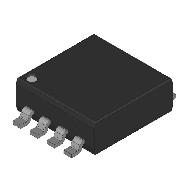
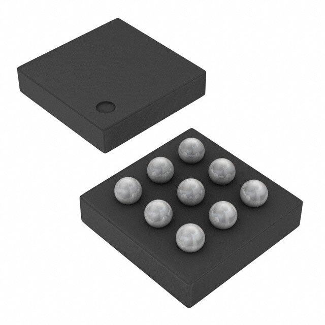
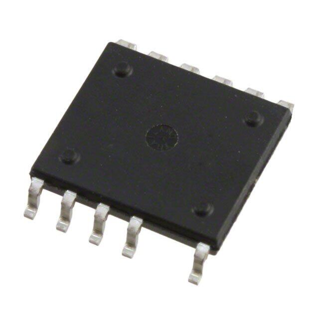
PCA9550 NXP Semiconductors 2-bit I2C-bus LED driver with programmable blink rates n ESD protection exceeds 2000V HBM per JESD22-A114, 150V MM per JESD22-A115 and 1000V CDM per JESD22-C101 n Latch-up testing is done to JEDEC Standard JESD78 which exceeds 100mA n Packages offered: SO8, TSSOP8 (MSOP8), HVSON8 3. Ordering information Table 1. Ordering information Type number Package Name Description Version PCA9550D SO8 plastic small outline package; 8leads; body width 3.9mm SOT96-1 PCA9550DP TSSOP8[1] plastic thin shrink small outline package; 8leads; body width 3mm SOT505-1 PCA9550TK HVSON8 plasticthermalenhancedverythinsmalloutlinepackage;noleads;8terminals; SOT908-1 body 3· 3· 0.85mm [1] Also known as MSOP8. 3.1 Ordering options Table 2. Ordering options Type number Topside mark Temperature range PCA9550D PCA9550 T =- 40(cid:176) C to +85(cid:176) C amb PCA9550DP 9550 T =- 40(cid:176) C to +85(cid:176) C amb PCA9550TK 9550 T =- 40(cid:176) C to +85(cid:176) C amb 4. Block diagram A0 PCA9550 INPUT REGISTER SCL INPUT I2C-BUS LED SELECT (LS0) SDA FILTERS CONTROL REGISTER 0 VDD POWER-ON 1 LEDn RESET RESET PRESCALER 0 PWM0 BLINK0 REGISTER REGISTER PRESCALER 1 PWM1 BLINK1 OSCILLATOR REGISTER REGISTER VSS 002aad241 Only one I/O shown for clarity. Fig 1. Block diagram of PCA9550 PCA9550_5 © NXP B.V. 2008. All rights reserved. Product data sheet Rev. 05 — 13 October 2008 2 of 26
PCA9550 NXP Semiconductors 2-bit I2C-bus LED driver with programmable blink rates 5. Pinning information 5.1 Pinning A0 1 8 VDD A0 1 8 VDD LED0 2 7 SDA LED0 2 7 SDA PCA9550D PCA9550DP LED1 3 6 SCL LED1 3 6 SCL VSS 4 5 RESET VSS 4 5 RESET 002aad238 002aad239 Fig 2. Pin configuration for SO8 Fig 3. Pin configuration for TSSOP8 terminal 1 index area A0 1 8 VDD LED0 2 7 SDA PCA9550TK LED1 3 6 SCL VSS 4 5 RESET 002aad240 Transparent top view Fig 4. Pin configuration for HVSON8 5.2 Pin description Table 3. Pin description Symbol Pin Description A0 1 address input 0 LED0 2 LED driver 0 LED1 3 LED driver 1 V 4 supply ground SS RESET 5 activeLOW reset input SCL 6 serial clock line SDA 7 serial data line V 8 supply voltage DD PCA9550_5 © NXP B.V. 2008. All rights reserved. Product data sheet Rev. 05 — 13 October 2008 3 of 26
PCA9550 NXP Semiconductors 2-bit I2C-bus LED driver with programmable blink rates 6. Functional description Refer toFigure 1 “Block diagram of PCA9550”. 6.1 Device address Following a START condition, the bus master must output the address of the slave it is accessing. The address of the PCA9550 is shown inFigure5. To conserve power, no internalpull-upresistorisincorporatedonthehardwareselectableaddresspinanditmust be pulled HIGH or LOW. slave address 1 1 0 0 0 0 A0 R/W fixed hardware selectable 002aad242 Fig 5. PCA9550 slave address Thelastbitoftheaddressbytedefinestheoperationtobeperformed.Whensettologic1 a read is selected, while a logic0 selects a write operation. 6.2 Control register Followingthesuccessfulacknowledgementoftheslaveaddress,thebusmasterwillsend a byte to the PCA9550, which will be stored in the Control register. 0 0 0 AI 0 B2 B1 B0 Auto-Increment flag register address 002aad243 Reset state: 00h Fig 6. Control register The lowest 3bits are used as a pointer to determine which register will be accessed. If the Auto-Increment (AI) flag is set, the three low order bits of the Control register are automatically incremented after a read or write. This allows the user to program the registerssequentially.Thecontentsofthesebitswillrolloverto‘000’afterthelastregister is accessed. When the Auto-Increment flag is set (AI=1) and a read sequence is initiated, the sequence must start by reading a register different from the input register (B2B1B0„ 000). Only the 3 least significant bits are affected by the AI flag. Unused bits must be programmed with zeroes. PCA9550_5 © NXP B.V. 2008. All rights reserved. Product data sheet Rev. 05 — 13 October 2008 4 of 26
PCA9550 NXP Semiconductors 2-bit I2C-bus LED driver with programmable blink rates 6.2.1 Control register definition Table 4. Register summary B2 B1 B0 Register name Access Description 0 0 0 INPUT read only input register 0 0 1 PSC0 read/write frequency prescaler 0 0 1 0 PWM0 read/write PWM register 0 0 1 1 PSC1 read/write frequency prescaler 1 1 0 0 PWM1 read/write PWM register 1 1 0 1 LS0 read/write LED selector 6.3 Register descriptions 6.3.1 INPUT - Input register The INPUT register reflects the state of the device pins. Writes to this register will be acknowledged but will have no effect. Table 5. INPUT - Input register description Bit 7 6 5 4 3 2 1 0 Symbol not used LED1 LED0 Default 0 0 0 0 0 0 X X Remark:Thedefaultvalue‘X’isdeterminedbytheexternallyappliedlogiclevel(normally logic1) when used for directly driving LED with pull-up to V . DD 6.3.2 PSC0 - Frequency Prescaler 0 PSC0 is used to program the period of the PWM output. The period of BLINK0=(PSC0+1)/44. Table 6. PSC0 - Frequency Prescaler0 register description Bit 7 6 5 4 3 2 1 0 Symbol PSC0[7] PSC0[6] PSC0[5] PSC0[4] PSC0[3] PSC0[2] PSC0[1] PSC0[0] Default 1 1 1 1 1 1 1 1 6.3.3 PWM0 - Pulse Width Modulation 0 ThePWM0registerdeterminesthedutycycleofBLINK0.TheoutputsareLOW(LEDoff) when the count is less than the value in PWM0 and HIGH when it is greater. If PWM0 is programmed with 00h, then the PWM0 output is always LOW. The duty cycle of BLINK0=(256- PWM0)/256. Table 7. PWM0 - Pulse Width Modulation 0 register description Bit 7 6 5 4 3 2 1 0 Symbol PWM0 PWM0 PWM0 PWM0 PWM0 PWM0 PWM0 PWM0 [7] [6] [5] [4] [3] [2] [1] [0] Default 1 0 0 0 0 0 0 0 PCA9550_5 © NXP B.V. 2008. All rights reserved. Product data sheet Rev. 05 — 13 October 2008 5 of 26
PCA9550 NXP Semiconductors 2-bit I2C-bus LED driver with programmable blink rates 6.3.4 PSC1 - Frequency Prescaler 1 PSC1 is used to program the period of the PWM output. The period of BLINK1=(PSC1+1)/44. Table 8. PSC1 - Frequency Prescaler1 register description Bit 7 6 5 4 3 2 1 0 Symbol PSC1[7] PSC1[6] PSC1[5] PSC1[4] PSC1[3] PSC1[2] PSC1[1] PSC1[0] Default 1 1 1 1 1 1 1 1 6.3.5 PWM1 - Pulse Width Modulation 1 ThePWM1registerdeterminesthedutycycleofBLINK1.TheoutputsareLOW(LEDoff) when the count is less than the value in PWM1 and HIGH when it is greater. If PWM1 is programmed with 00h, then the PWM1 output is always LOW. The duty cycle of BLINK1=(256- PWM1)/256. Table 9. PWM1 - Pulse Width Modulation 1 register description Bit 7 6 5 4 3 2 1 0 Symbol PWM1 PWM1 PWM1 PWM1 PWM1 PWM1 PWM1 PWM1 [7] [6] [5] [4] [3] [2] [1] [0] Default 1 0 0 0 0 0 0 0 6.3.6 LS0 - LED selector The LS0 LED select register determines the source of the LED data. 00=output is set LOW (LED on) 01=output is set high-impedance (LED off; default) 10=output blinks at PWM0 rate 11=output blinks at PWM1 rate Table 10. LS0 - LED selector register description Bit 7 6 5 4 3 2 1 0 Symbol LS0[7:4] LED1 LED0 Default 1 1 1 1 0 1 0 1 PCA9550_5 © NXP B.V. 2008. All rights reserved. Product data sheet Rev. 05 — 13 October 2008 6 of 26
PCA9550 NXP Semiconductors 2-bit I2C-bus LED driver with programmable blink rates 6.4 Pins used as GPIOs LED pins not used to control LEDs can be used as General Purpose Input/Outputs (GPIOs). For use as input, set LEDn to high-impedance (01) and then read the pin state via the Input register. For use as output, connect external pull-up resistor to the pin and size it according to the DC recommended operating characteristics. LEDn output pin is HIGH when the output is programmedashigh-impedance,andLOWwhentheoutputisprogrammedLOWthrough theLEDselectorregister(LS0).Theoutputcanbepulse-widthcontrolledwhenPWM0or PWM1 are used. 6.5 Power-on reset When power is applied to V , an internal Power-On Reset (POR) holds the PCA9550 in DD aresetconditionuntilV hasreachedV .Atthatpoint,theresetconditionisreleased DD POR and the PCA9550 registers are initialized to their default states, all the outputs in the OFFstate. Thereafter, V must be lowered below 0.2V to reset the device. DD 6.6 External RESET AresetcanbeaccomplishedbyholdingtheRESETpinLOWforaminimumoft .The w(rst) PCA9550 registers and I2C-bus state machine will be held in their default states until the RESET input is once again HIGH. This input requires a pull-up resistor to V if no active connection is used. DD PCA9550_5 © NXP B.V. 2008. All rights reserved. Product data sheet Rev. 05 — 13 October 2008 7 of 26
PCA9550 NXP Semiconductors 2-bit I2C-bus LED driver with programmable blink rates 7. Characteristics of the I2C-bus TheI2C-busisfor2-way,2-linecommunicationbetweendifferentICsormodules.Thetwo lines are a serial data line (SDA) and a serial clock line (SCL). Both lines must be connected to a positive supply via a pull-up resistor when connected to the output stages of a device. Data transfer may be initiated only when the bus is not busy. 7.1 Bit transfer Onedatabitistransferredduringeachclockpulse.ThedataontheSDAlinemustremain stable during the HIGH period of the clock pulse as changes in the data line at this time will be interpreted as control signals (seeFigure7). SDA SCL data line change stable; of data data valid allowed mba607 Fig 7. Bit transfer 7.1.1 START and STOP conditions Both data and clock lines remain HIGH when the bus is not busy. A HIGH-to-LOW transition of the data line while the clock is HIGH is defined as the START condition (S). ALOW-to-HIGHtransitionofthedatalinewhiletheclockisHIGHisdefinedastheSTOP condition (P) (seeFigure8). SDA SDA SCL SCL S P START condition STOP condition mba608 Fig 8. Definition of START and STOP conditions 7.2 System configuration A device generating a message is a ‘transmitter’; a device receiving is the ‘receiver’. The device that controls the message is the ‘master’ and the devices which are controlled by the master are the ‘slaves’ (seeFigure9). PCA9550_5 © NXP B.V. 2008. All rights reserved. Product data sheet Rev. 05 — 13 October 2008 8 of 26
PCA9550 NXP Semiconductors 2-bit I2C-bus LED driver with programmable blink rates SDA SCL MASTER SLAVE SLAVE MASTER MASTER I2C-BUS TRANSMITTER/ RECEIVER TRANSMITTER/ TRANSMITTER TRANSMITTER/ MULTIPLEXER RECEIVER RECEIVER RECEIVER SLAVE 002aaa966 Fig 9. System configuration 7.3 Acknowledge The number of data bytes transferred between the START and the STOP conditions from transmitter to receiver is not limited. Each byte of eightbits is followed by one acknowledge bit. The acknowledge bit is a HIGH level put on the bus by the transmitter, whereas the master generates an extra acknowledge related clock pulse. Aslavereceiverwhichisaddressedmustgenerateanacknowledgeafterthereceptionof each byte. Also a master must generate an acknowledge after the reception of each byte that has been clocked out of the slave transmitter. The device that acknowledges has to pulldowntheSDAlineduringtheacknowledgeclockpulse,sothattheSDAlineisstable LOW during the HIGH period of the acknowledge related clock pulse; set-up and hold times must be taken into account. A master receiver must signal an end of data to the transmitter by not generating an acknowledge on the last byte that has been clocked out of the slave. In this event, the transmitter must leave the data line HIGH to enable the master to generate a STOP condition. data output by transmitter not acknowledge data output by receiver acknowledge SCL from master 1 2 8 9 S clock pulse for START acknowledgement condition 002aaa987 Fig 10. Acknowledgement on the I2C-bus PCA9550_5 © NXP B.V. 2008. All rights reserved. Product data sheet Rev. 05 — 13 October 2008 9 of 26
PCA9550 NXP Semiconductors 2-bit I2C-bus LED driver with programmable blink rates 7.4 Bus transactions SCL 1 2 3 4 5 6 7 8 9 slave address command byte data to register SDA S 1 1 0 0 0 0 A0 0 A 0 0 0 AI 0 B2 B1 B0 A DATA 1 A START condition R/W acknowledge acknowledge acknowledge from slave from slave from slave write to register tv(Q) data out from port DATA 1 VALID 002aad268 Fig 11. Write to register slave address command byte SDA S 1 1 0 0 0 0 A0 0 A 0 0 0 AI 0 B2 B1 B0 A (cont.) START condition R/W acknowledge acknowledge from slave from slave slave address data from register data from register (cont.) S 1 1 0 0 0 0 A0 1 A DATA (first byte) A DATA (last byte) NA P Auto-Increment (repeated) R/W register address acknowledge no acknowledge STOP START condition acknowledge if AI = 1 from master from master condition from slave at this moment master-transmitter becomes master-receiver and slave-receiver becomes slave-transmitter 002aad269 Fig 12. Read from register no acknowledge from master slave address data from port data from port SDA S 1 1 0 0 0 0 A0 1 A DATA 1 A DATA 4 NA P START condition R/W acknowledge acknowledge STOP from slave from master condition read from port th(D) tsu(D) data into port DATA 1 DATA 2 DATA 3 DATA 4 002aad270 Remark:This figure assumes the command byte has previously been programmed with 00h. Fig 13. Read input port register PCA9550_5 © NXP B.V. 2008. All rights reserved. Product data sheet Rev. 05 — 13 October 2008 10 of 26
PCA9550 NXP Semiconductors 2-bit I2C-bus LED driver with programmable blink rates 8. Application design-in information 5 V 5 V 10 kW 10 kW 10 kW I2C-BUS/SMBus VDD MASTER PCA9550 SDA SDA LED0 SCL SCL LED1 RESET A0 VSS 002aad271 Fig 14. Typical application 8.1 Minimizing I when the I/Os are used to control LEDs DD When the I/Os are used to control LEDs, they are normally connected to V through a DD resistor as shown inFigure14. Since the LED acts as a diode, when the LED is off the I/OV is about 1.2V less than V . The supply current, I , increases as V becomes I DD DD I lower than V . DD Designs needing to minimize current consumption, such as battery power applications, shouldconsidermaintainingtheI/OpinsgreaterthanorequaltoV whentheLEDisoff. DD Figure15 shows a high value resistor in parallel with the LED.Figure16 shows V less DD than the LED supply voltage by at least 1.2V. Both of these methods maintain the I/OV I at or above V and prevents additional supply current consumption when the LED is off. DD 3.3 V 5 V VDD VDD LED 100 kW VDD LED LEDn LEDn 002aac189 002aac190 Fig 15. High value resistor in parallel with Fig 16. Device supplied by a lower voltage the LED PCA9550_5 © NXP B.V. 2008. All rights reserved. Product data sheet Rev. 05 — 13 October 2008 11 of 26
PCA9550 NXP Semiconductors 2-bit I2C-bus LED driver with programmable blink rates 8.2 Programming example The following example will show how to set LED0 to blink at 1Hz at a 50% duty cycle. LED1 will be set to blink at 4Hz and at a 25% duty cycle. Table 11. Programming PCA9550 Program sequence I2C-bus START S PCA9550 address with A0=LOW C0h PSC0 subaddress + Auto-Increment 11h Set prescaler PSC0 to achieve a period of 1second: 2Bh PSC0+1 Blink period = 1 = ------------------------ 44 PSC0=43 Set PWM0 duty cycle to 50%: 80h 256–PWM0 -------------------------------- = 0.5 256 PWM0=128 Set prescaler PSC1 to achieve a period of 0.25 seconds: 0Ah PSC1+1 Blink period = 0.25 = ------------------------ 44 PSC1=10 Set PWM1 output duty cycle to 25%: C0h 256–PWM1 -------------------------------- = 0.25 256 PWM1=192 Set LED0 to PWM0, and set LED1 to blink at PWM1 0Eh STOP P 9. Limiting values Table 12. Limiting values In accordance with the Absolute Maximum Rating System (IEC 60134). Symbol Parameter Conditions Min Max Unit V supply voltage - 0.5 +6.0 V DD V voltage on an input/output pin V - 0.5 5.5 V I/O SS I output current on pin LEDn - – 25 mA O(LEDn) I ground supply current - 50 mA SS P total power dissipation - 400 mW tot T storage temperature - 65 +150 (cid:176) C stg T ambient temperature operating - 40 +85 (cid:176) C amb PCA9550_5 © NXP B.V. 2008. All rights reserved. Product data sheet Rev. 05 — 13 October 2008 12 of 26
PCA9550 NXP Semiconductors 2-bit I2C-bus LED driver with programmable blink rates 10. Static characteristics Table 13. Static characteristics V =2.3V to 5.5V; V =0V; T =- 40(cid:176) C to +85(cid:176) C; unless otherwise specified. DD SS amb Symbol Parameter Conditions Min Typ[1] Max Unit Supplies V supply voltage 2.3 - 5.5 V DD I supply current operating mode; V =5.5V; noload; - 350 500 m A DD DD V =V or V ; f =100kHz I DD SS SCL I standby current Standby mode; V =5.5V; noload; - 1.9 3.0 m A stb DD V =V orV ; f =0kHz I DD SS SCL V power-on reset voltage no load; V =V or V [2] 1.4 1.7 2.2 V POR I DD SS Input SCL; input/output SDA V LOW-level input voltage - 0.5 - +0.3V V IL DD V HIGH-level input voltage 0.7V - 5.5 V IH DD I LOW-level output current V =0.4V 3 6.5 - mA OL OL I leakage current V =V =V - 1 - +1 m A L I DD SS C input capacitance V =V - 3.7 5 pF i I SS I/Os V LOW-level input voltage - 0.5 - +0.8 V IL V HIGH-level input voltage 2.0 - 5.5 V IH I LOW-level output current V =0.4V OL OL V =2.3V [3] 6 9 - mA DD V =3.0V [3] 8 11 - mA DD V =5.0V [3] 10 14 - mA DD V =0.7V OL V =2.3V [3] 11 14 - mA DD V =3.0V [3] 14 18 - mA DD V =5.0V [3] 17 24 - mA DD I input leakage current V =3.6V; V =0V or V - 1 - +1 m A LI DD I DD C input/output capacitance - 2.1 5 pF io Select inputs A0;RESET V LOW-level input voltage - 0.5 - +0.8 V IL V HIGH-level input voltage 2.0 - 5.5 V IH I input leakage current - 1 - +1 m A LI C input capacitance V =V - 2.3 5 pF i I SS [1] Typical limits at V =3.3V, T =25(cid:176) C. DD amb [2] V must be lowered to 0.2V in order to reset part. DD [3] Each I/O must be externally limited to a maximum of 25mA and the device must be limited to a maximum current of 50mA. PCA9550_5 © NXP B.V. 2008. All rights reserved. Product data sheet Rev. 05 — 13 October 2008 13 of 26
PCA9550 NXP Semiconductors 2-bit I2C-bus LED driver with programmable blink rates 002aac191 002aac192 20 % 20 % (1) (1) percent percent variation variation 0 % 0 % (2) (2) - 20 % - 20 % (3) (3) - 40 % - 40 % - 40 - 20 0 20 40 60 80 100 - 40 - 20 0 20 40 60 80 100 Tamb ((cid:176)C) Tamb ((cid:176)C) (1) maximum (1) maximum (2) average (2) average (3) minimum (3) minimum Fig 17. Typical frequency variation over process at Fig 18. Typical frequency variation over process at V =2.3V to 3.0V V =3.0V to 5.5V DD DD PCA9550_5 © NXP B.V. 2008. All rights reserved. Product data sheet Rev. 05 — 13 October 2008 14 of 26
PCA9550 NXP Semiconductors 2-bit I2C-bus LED driver with programmable blink rates 11. Dynamic characteristics Table 14. Dynamic characteristics Symbol Parameter Conditions Standard-mode Fast-mode I2C-bus Unit I2C-bus Min Max Min Max f SCL clock frequency 0 100 0 400 kHz SCL t bus free time between a STOP and 4.7 - 1.3 - m s BUF START condition t hold time (repeated) START condition 4.0 - 0.6 - m s HD;STA t set-up time for a repeated START 4.7 - 0.6 - m s SU;STA condition t set-up time for STOP condition 4.0 - 0.6 - m s SU;STO t data hold time 0 - 0 - ns HD;DAT t data valid acknowledge time [1] - 600 - 600 ns VD;ACK t data valid time LOW-level [2] - 600 - 600 ns VD;DAT HIGH-level [2] - 1500 - 600 ns t data set-up time 250 - 100 - ns SU;DAT t LOW period of the SCL clock 4.7 - 1.3 - m s LOW t HIGH period of the SCL clock 4.0 - 0.6 - m s HIGH t rise time of both SDA and SCL signals - 1000 20+0.1C [3] 300 ns r b t fall time of both SDA and SCL signals - 300 20+0.1C [3] 300 ns f b t pulse width of spikes that must be - 50 - 50 ns SP suppressed by the input filter Port timing t data output valid time - 200 - 200 ns v(Q) t data input set-up time 100 - 100 - ns su(D) t data input hold time 1 - 1 - m s h(D) Reset t reset pulse width 6 - 6 - ns w(rst) t reset recovery time 0 - 0 - ns rec(rst) t reset time [4][5] 400 - 400 - ns rst [1] t = time for Acknowledgement signal from SCL LOW to SDA (out) LOW. VD;ACK [2] t = minimum time for SDA data output to be valid following SCL LOW. VD;DAT [3] C =total capacitance of one bus line in pF. b [4] Resetting the device while actively communicating on the bus may cause glitches or errant STOP conditions. [5] Upon reset, the full delay will be the sum of t and the RC time constant of the SDA bus. rst PCA9550_5 © NXP B.V. 2008. All rights reserved. Product data sheet Rev. 05 — 13 October 2008 15 of 26
PCA9550 NXP Semiconductors 2-bit I2C-bus LED driver with programmable blink rates START ACK or read cycle SCL SDA 30 % trst RESET 50 % 50 % 50 % trec(rst) tw(rst) trst LEDn 50 % LED off 002aac193 Fig 19. Definition ofRESET timing SDA tBUF tr tf tHD;STA tSP tLOW SCL tHD;STA tSU;STA tSU;STO P S tHD;DAT tHIGH tSU;DAT Sr P 002aaa986 Fig 20. Definition of timing PCA9550_5 © NXP B.V. 2008. All rights reserved. Product data sheet Rev. 05 — 13 October 2008 16 of 26
PCA9550 NXP Semiconductors 2-bit I2C-bus LED driver with programmable blink rates START bit 7 STOP bit 6 bit 0 acknowledge protocol condition MSB condition (A6) (R/W) (A) (S) (A7) (P) tSU;STA tLOW tHIGH 1/fSCL SCL tBUF tf tr SDA tHD;STA tSU;DAT tHD;DAT tVD;DAT tVD;ACK tSU;STO 002aab175 Rise and fall times refer to V and V . IL IH Fig 21. I2C-bus timing diagram 12. Test information VDD open VDD RL VSS 500 W VI VO PULSE DUT GENERATOR RT C50L pF 002aab880 R = load resistor for LEDn. R for SDA and SCL > 1kW (3mA or less current). L L C = load capacitance includes jig and probe capacitance. L R = termination resistance should be equal to the output impedance Z of the pulse generators. T o Fig 22. Test circuitry for switching times PCA9550_5 © NXP B.V. 2008. All rights reserved. Product data sheet Rev. 05 — 13 October 2008 17 of 26
PCA9550 NXP Semiconductors 2-bit I2C-bus LED driver with programmable blink rates 13. Package outline SO8: plastic small outline package; 8 leads; body width 3.9 mm SOT96-1 D E A X c y HE v M A Z 8 5 Q A2 A1 (A 3 ) A pin 1 index q Lp 1 4 L e w M detail X bp 0 2.5 5 mm scale DIMENSIONS (inch dimensions are derived from the original mm dimensions) UNIT mAax. A1 A2 A3 bp c D(1) E(2) e HE L Lp Q v w y Z(1) q 0.25 1.45 0.49 0.25 5.0 4.0 6.2 1.0 0.7 0.7 mm 1.75 0.25 1.27 1.05 0.25 0.25 0.1 0.10 1.25 0.36 0.19 4.8 3.8 5.8 0.4 0.6 0.3 8o 0.010 0.057 0.019 0.0100 0.20 0.16 0.244 0.039 0.028 0.028 0o inches 0.069 0.01 0.05 0.041 0.01 0.01 0.004 0.004 0.049 0.014 0.0075 0.19 0.15 0.228 0.016 0.024 0.012 Notes 1. Plastic or metal protrusions of 0.15 mm (0.006 inch) maximum per side are not included. 2. Plastic or metal protrusions of 0.25 mm (0.01 inch) maximum per side are not included. OUTLINE REFERENCES EUROPEAN ISSUE DATE VERSION IEC JEDEC JEITA PROJECTION 99-12-27 SOT96-1 076E03 MS-012 03-02-18 Fig 23. Package outline SOT96-1 (SO8) PCA9550_5 © NXP B.V. 2008. All rights reserved. Product data sheet Rev. 05 — 13 October 2008 18 of 26
PCA9550 NXP Semiconductors 2-bit I2C-bus LED driver with programmable blink rates TSSOP8: plastic thin shrink small outline package; 8 leads; body width 3 mm SOT505-1 D E A X c y HE v M A Z 8 5 A2 A1 (A3) A pin 1 index q Lp L 1 4 detail X e w M bp 0 2.5 5 mm scale DIMENSIONS (mm are the original dimensions) UNIT mAax. A1 A2 A3 bp c D(1) E(2) e HE L Lp v w y Z(1) q mm 1.1 0.15 0.95 0.25 0.45 0.28 3.1 3.1 0.65 5.1 0.94 0.7 0.1 0.1 0.1 0.70 6(cid:176) 0.05 0.80 0.25 0.15 2.9 2.9 4.7 0.4 0.35 0(cid:176) Notes 1. Plastic or metal protrusions of 0.15 mm maximum per side are not included. 2. Plastic or metal protrusions of 0.25 mm maximum per side are not included. OUTLINE REFERENCES EUROPEAN ISSUE DATE VERSION IEC JEDEC JEITA PROJECTION 99-04-09 SOT505-1 03-02-18 Fig 24. Package outline SOT505-1 (TSSOP8) PCA9550_5 © NXP B.V. 2008. All rights reserved. Product data sheet Rev. 05 — 13 October 2008 19 of 26
PCA9550 NXP Semiconductors 2-bit I2C-bus LED driver with programmable blink rates HVSON8: plastic thermal enhanced very thin small outline package; no leads; 8 terminals; body 3 x 3 x 0.85 mm SOT908-1 0 1 2 mm scale X D B A E A A1 c detail X terminal 1 index area tinedrmexin aarl e1a e e1 b v M C A B C 1 4 w M C y1C y L exposed tie bar (4· ) Eh exposed tie bar (4· ) 8 5 Dh DIMENSIONS (mm are the original dimensions) A(1) UNIT max. A1 b c D(1) Dh E(1) Eh e e1 L v w y y1 0.05 0.3 3.1 2.25 3.1 1.65 0.5 mm 1 0.2 0.5 1.5 0.1 0.05 0.05 0.1 0.00 0.2 2.9 1.95 2.9 1.35 0.3 Note 1. Plastic or metal protrusions of 0.075 mm maximum per side are not included. OUTLINE REFERENCES EUROPEAN ISSUE DATE VERSION IEC JEDEC JEITA PROJECTION 05-09-26 SOT908-1 MO-229 05-10-05 Fig 25. Package outline SOT908-1 (HVSON8) PCA9550_5 © NXP B.V. 2008. All rights reserved. Product data sheet Rev. 05 — 13 October 2008 20 of 26
PCA9550 NXP Semiconductors 2-bit I2C-bus LED driver with programmable blink rates 14. Handling information Inputs and outputs are protected against electrostatic discharge in normal handling. However,tobecompletelysafeyoumusttakenormalprecautionsappropriatetohandling integrated circuits. 15. Soldering of SMD packages Thistextprovidesaverybriefinsightintoacomplextechnology.Amorein-depthaccount of soldering ICs can be found in Application NoteAN10365 “Surface mount reflow soldering description”. 15.1 Introduction to soldering Soldering is one of the most common methods through which packages are attached to PrintedCircuitBoards(PCBs),toformelectricalcircuits.Thesolderedjointprovidesboth the mechanical and the electrical connection. There is no single soldering method that is ideal for all IC packages. Wave soldering is often preferred when through-hole and Surface Mount Devices (SMDs) are mixed on one printed wiring board; however, it is not suitable for fine pitch SMDs. Reflow soldering is ideal for the small pitches and high densities that come with increased miniaturization. 15.2 Wave and reflow soldering Wavesolderingisajoiningtechnologyinwhichthejointsaremadebysoldercomingfrom a standing wave of liquid solder. The wave soldering process is suitable for the following: • Through-hole components • Leaded or leadless SMDs, which are glued to the surface of the printed circuit board Not all SMDs can be wave soldered. Packages with solder balls, and some leadless packages which have solder lands underneath the body, cannot be wave soldered. Also, leaded SMDs with leads having a pitch smaller than ~0.6mm cannot be wave soldered, due to an increased probability of bridging. The reflow soldering process involves applying solder paste to a board, followed by component placement and exposure to a temperature profile. Leaded packages, packages with solder balls, and leadless packages are all reflow solderable. Key characteristics in both wave and reflow soldering are: • Board specifications, including the board finish, solder masks and vias • Package footprints, including solder thieves and orientation • The moisture sensitivity level of the packages • Package placement • Inspection and repair • Lead-free soldering versus SnPb soldering 15.3 Wave soldering Key characteristics in wave soldering are: PCA9550_5 © NXP B.V. 2008. All rights reserved. Product data sheet Rev. 05 — 13 October 2008 21 of 26
PCA9550 NXP Semiconductors 2-bit I2C-bus LED driver with programmable blink rates • Process issues, such as application of adhesive and flux, clinching of leads, board transport, the solder wave parameters, and the time during which components are exposed to the wave • Solder bath specifications, including temperature and impurities 15.4 Reflow soldering Key characteristics in reflow soldering are: • Lead-freeversusSnPbsoldering;notethatalead-freereflowprocessusuallyleadsto higher minimum peak temperatures (seeFigure26) than a SnPb process, thus reducing the process window • Solder paste printing issues including smearing, release, and adjusting the process window for a mix of large and small components on one board • Reflow temperature profile; this profile includes preheat, reflow (in which the board is heated to the peak temperature) and cooling down. It is imperative that the peak temperatureishighenoughforthesoldertomakereliablesolderjoints(asolderpaste characteristic). In addition, the peak temperature must be low enough that the packages and/or boards are not damaged. The peak temperature of the package depends on package thickness and volume and is classified in accordance with Table15 and16 Table 15. SnPb eutectic process (from J-STD-020C) Package thickness (mm) Package reflow temperature ((cid:176) C) Volume (mm3) < 350 ‡ 350 < 2.5 235 220 ‡ 2.5 220 220 Table 16. Lead-free process (from J-STD-020C) Package thickness (mm) Package reflow temperature ((cid:176) C) Volume (mm3) < 350 350 to 2000 > 2000 < 1.6 260 260 260 1.6 to 2.5 260 250 245 > 2.5 250 245 245 Moisture sensitivity precautions, as indicated on the packing, must be respected at all times. Studies have shown that small packages reach higher temperatures during reflow soldering, seeFigure26. PCA9550_5 © NXP B.V. 2008. All rights reserved. Product data sheet Rev. 05 — 13 October 2008 22 of 26
PCA9550 NXP Semiconductors 2-bit I2C-bus LED driver with programmable blink rates maximum peak temperature = MSL limit, damage level temperature minimum peak temperature = minimum soldering temperature peak temperature time 001aac844 MSL: Moisture Sensitivity Level Fig 26. Temperature profiles for large and small components For further information on temperature profiles, refer to Application NoteAN10365 “Surface mount reflow soldering description”. 16. Abbreviations Table 17. Abbreviations Acronym Description AI Auto-Increment CDM Charged Device Model DSP Digital Signal Processor DUT Device Under Test ESD ElectroStatic Discharge GPIO General Purpose Input/Output HBM Human Body Model I2C-bus Inter IC bus I/O Input/Output IC Integrated Circuit LED Light Emitting Diode MCU MicroController Unit MM Machine Model MPU MicroProcessor Unit POR Power-On Reset PWM Pulse Width Modulation RC Resistor-Capacitor network SMBus System Management Bus PCA9550_5 © NXP B.V. 2008. All rights reserved. Product data sheet Rev. 05 — 13 October 2008 23 of 26
PCA9550 NXP Semiconductors 2-bit I2C-bus LED driver with programmable blink rates 17. Revision history Table 18. Revision history Document ID Release date Data sheet status Change notice Supersedes PCA9550_5 20081013 Product data sheet - PCA9550_4 Modifications: • Section 8.1 “Minimizing I when the I/Os are used to control LEDs”, 1st paragraph, DD 3rdsentence changed from “The supply current, I , increases as V becomes lower than DD I V andisspecifiedasD I inTable13“Staticcharacteristics”.”to“Thesupplycurrent,I , DD DD DD increases as V becomes lower than V .” I DD • Table 13 “Static characteristics”, sub-section “Supplies”: removedD I characteristic DD • Table 13 “Static characteristics”, sub-section “I/Os”, symbol I , LOW-level output current: OL – condition V =0.4V; V =2.3V: changed Min value from “9mA” to “6mA”; OL DD changedTyp value from “-” to “9mA” – condition V =0.4V; V =3.0V: changed Min value from “11mA” to “8mA”; OL DD changedTyp value from “-” to “11mA” – condition V =0.4V; V =5.0V: changed Min value from “14mA” to “10mA”; OL DD changedTyp value from “-” to “14mA” – condition V =0.7V; V =2.3V: changed Min value from “14mA” to “11mA”; OL DD changedTyp value from “-” to “14mA” – condition V =0.7V; V =3.0V: changed Min value from “18mA” to “14mA”; OL DD changedTyp value from “-” to “18mA” – condition V =0.7V; V =5.0V: changed Min value from “24mA” to “17mA”; OL DD changedTyp value from “-” to “24mA” • updated soldering information PCA9550_4 20080107 Product data sheet - PCA9550_3 PCA9550_3 20041001 Product data sheet - PCA9550_2 (939775013719) PCA9550_2 20030502 Product data ECN853-239629859of PCA9550_1 (939775011461) 24Apr2003 PCA9550_1 20021213 Product data ECN853-239629264of - (939775010857) 09Dec2002 PCA9550_5 © NXP B.V. 2008. All rights reserved. Product data sheet Rev. 05 — 13 October 2008 24 of 26
PCA9550 NXP Semiconductors 2-bit I2C-bus LED driver with programmable blink rates 18. Legal information 18.1 Data sheet status Document status[1][2] Product status[3] Definition Objective [short] data sheet Development This document contains data from the objective specification for product development. Preliminary [short] data sheet Qualification This document contains data from the preliminary specification. Product [short] data sheet Production This document contains the product specification. [1] Please consult the most recently issued document before initiating or completing a design. [2] The term ‘short data sheet’ is explained in section “Definitions”. [3] Theproductstatusofdevice(s)describedinthisdocumentmayhavechangedsincethisdocumentwaspublishedandmaydifferincaseofmultipledevices.Thelatestproductstatus information is available on the Internet at URLhttp://www.nxp.com. 18.2 Definitions to result in personal injury, death or severe property or environmental damage. NXP Semiconductors accepts no liability for inclusion and/or use of NXP Semiconductors products in such equipment or applications and Draft —The document is a draft version only. The content is still under therefore such inclusion and/or use is at the customer’s own risk. internal review and subject to formal approval, which may result in modifications or additions. NXP Semiconductors does not give any Applications —Applications that are described herein for any of these representations or warranties as to the accuracy or completeness of products are for illustrative purposes only. NXP Semiconductors makes no informationincludedhereinandshallhavenoliabilityfortheconsequencesof representation or warranty that such applications will be suitable for the use of such information. specified use without further testing or modification. Short data sheet —A short data sheet is an extract from a full data sheet Limiting values —Stress above one or more limiting values (as defined in withthesameproducttypenumber(s)andtitle.Ashortdatasheetisintended theAbsoluteMaximumRatingsSystemofIEC60134)maycausepermanent forquickreferenceonlyandshouldnotbereliedupontocontaindetailedand damagetothedevice.Limitingvaluesarestressratingsonlyandoperationof full information. For detailed and full information see the relevant full data the device at these or any other conditions above those given in the sheet, which is available on request via the local NXP Semiconductors sales Characteristics sections of this document is not implied. Exposure to limiting office. In case of any inconsistency or conflict with the short data sheet, the values for extended periods may affect device reliability. full data sheet shall prevail. Terms and conditions of sale —NXP Semiconductors products are sold subjecttothegeneraltermsandconditionsofcommercialsale,aspublished 18.3 Disclaimers athttp://www.nxp.com/profile/terms, including those pertaining to warranty, intellectual property rights infringement and limitation of liability, unless explicitly otherwise agreed to in writing by NXP Semiconductors. In case of General —Information in this document is believed to be accurate and any inconsistency or conflict between information in this document and such reliable.However,NXPSemiconductorsdoesnotgiveanyrepresentationsor terms and conditions, the latter will prevail. warranties,expressedorimplied,astotheaccuracyorcompletenessofsuch No offer to sell or license —Nothing in this document may be interpreted information and shall have no liability for the consequences of use of such or construed as an offer to sell products that is open for acceptance or the information. grant,conveyanceorimplicationofanylicenseunderanycopyrights,patents Right to make changes —NXPSemiconductorsreservestherighttomake or other industrial or intellectual property rights. changes to information published in this document, including without limitation specifications and product descriptions, at any time and without notice.Thisdocumentsupersedesandreplacesallinformationsuppliedprior 18.4 Trademarks to the publication hereof. Notice:Allreferencedbrands,productnames,servicenamesandtrademarks Suitability for use —NXP Semiconductors products are not designed, are the property of their respective owners. authorized or warranted to be suitable for use in medical, military, aircraft, space or life support equipment, nor in applications where failure or I2C-bus —logois a trademark of NXP B.V. malfunction of an NXP Semiconductors product can reasonably be expected 19. Contact information For more information, please visit:http://www.nxp.com For sales office addresses, please send an email to:salesaddresses@nxp.com PCA9550_5 © NXP B.V. 2008. All rights reserved. Product data sheet Rev. 05 — 13 October 2008 25 of 26
PCA9550 NXP Semiconductors 2-bit I2C-bus LED driver with programmable blink rates 20. Contents 1 General description. . . . . . . . . . . . . . . . . . . . . . 1 18 Legal information . . . . . . . . . . . . . . . . . . . . . . 25 2 Features . . . . . . . . . . . . . . . . . . . . . . . . . . . . . . . 1 18.1 Data sheet status. . . . . . . . . . . . . . . . . . . . . . 25 18.2 Definitions . . . . . . . . . . . . . . . . . . . . . . . . . . . 25 3 Ordering information. . . . . . . . . . . . . . . . . . . . . 2 18.3 Disclaimers. . . . . . . . . . . . . . . . . . . . . . . . . . . 25 3.1 Ordering options. . . . . . . . . . . . . . . . . . . . . . . . 2 18.4 Trademarks . . . . . . . . . . . . . . . . . . . . . . . . . . 25 4 Block diagram . . . . . . . . . . . . . . . . . . . . . . . . . . 2 19 Contact information . . . . . . . . . . . . . . . . . . . . 25 5 Pinning information. . . . . . . . . . . . . . . . . . . . . . 3 20 Contents. . . . . . . . . . . . . . . . . . . . . . . . . . . . . . 26 5.1 Pinning . . . . . . . . . . . . . . . . . . . . . . . . . . . . . . . 3 5.2 Pin description . . . . . . . . . . . . . . . . . . . . . . . . . 3 6 Functional description . . . . . . . . . . . . . . . . . . . 4 6.1 Device address. . . . . . . . . . . . . . . . . . . . . . . . . 4 6.2 Control register. . . . . . . . . . . . . . . . . . . . . . . . . 4 6.2.1 Control register definition . . . . . . . . . . . . . . . . . 5 6.3 Register descriptions . . . . . . . . . . . . . . . . . . . . 5 6.3.1 INPUT - Input register. . . . . . . . . . . . . . . . . . . . 5 6.3.2 PSC0 - Frequency Prescaler0. . . . . . . . . . . . . 5 6.3.3 PWM0 - Pulse Width Modulation0. . . . . . . . . . 5 6.3.4 PSC1 - Frequency Prescaler1. . . . . . . . . . . . . 6 6.3.5 PWM1 - Pulse Width Modulation1. . . . . . . . . . 6 6.3.6 LS0 - LED selector . . . . . . . . . . . . . . . . . . . . . . 6 6.4 Pins used as GPIOs. . . . . . . . . . . . . . . . . . . . . 7 6.5 Power-on reset . . . . . . . . . . . . . . . . . . . . . . . . . 7 6.6 ExternalRESET. . . . . . . . . . . . . . . . . . . . . . . . 7 7 Characteristics of the I2C-bus. . . . . . . . . . . . . . 8 7.1 Bit transfer . . . . . . . . . . . . . . . . . . . . . . . . . . . . 8 7.1.1 START and STOP conditions . . . . . . . . . . . . . . 8 7.2 System configuration . . . . . . . . . . . . . . . . . . . . 8 7.3 Acknowledge . . . . . . . . . . . . . . . . . . . . . . . . . . 9 7.4 Bus transactions. . . . . . . . . . . . . . . . . . . . . . . 10 8 Application design-in information . . . . . . . . . 11 8.1 Minimizing I when the I/Os are used DD to control LEDs. . . . . . . . . . . . . . . . . . . . . . . . 11 8.2 Programming example . . . . . . . . . . . . . . . . . . 12 9 Limiting values. . . . . . . . . . . . . . . . . . . . . . . . . 12 10 Static characteristics. . . . . . . . . . . . . . . . . . . . 13 11 Dynamic characteristics . . . . . . . . . . . . . . . . . 15 12 Test information. . . . . . . . . . . . . . . . . . . . . . . . 17 13 Package outline . . . . . . . . . . . . . . . . . . . . . . . . 18 14 Handling information. . . . . . . . . . . . . . . . . . . . 21 15 Soldering of SMD packages . . . . . . . . . . . . . . 21 15.1 Introduction to soldering. . . . . . . . . . . . . . . . . 21 15.2 Wave and reflow soldering . . . . . . . . . . . . . . . 21 15.3 Wave soldering. . . . . . . . . . . . . . . . . . . . . . . . 21 15.4 Reflow soldering. . . . . . . . . . . . . . . . . . . . . . . 22 16 Abbreviations. . . . . . . . . . . . . . . . . . . . . . . . . . 23 17 Revision history. . . . . . . . . . . . . . . . . . . . . . . . 24 Pleasebeawarethatimportantnoticesconcerningthisdocumentandtheproduct(s) described herein, have been included in section ‘Legal information’. © NXP B.V. 2008. All rights reserved. For more information, please visit: http://www.nxp.com For sales office addresses, please send an email to: salesaddresses@nxp.com Date of release: 13 October 2008 Document identifier: PCA9550_5
Mouser Electronics Authorized Distributor Click to View Pricing, Inventory, Delivery & Lifecycle Information: N XP: PCA9550D,112 PCA9550DP,118 PCA9550D,118