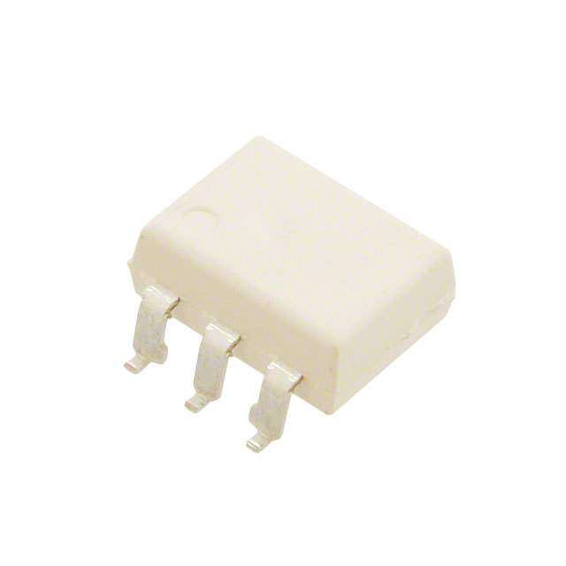
ICGOO在线商城 > 隔离器 > 光隔离器 - 三端双向可控硅,SCR输出 > PC3SD11NTZCF
- 型号: PC3SD11NTZCF
- 制造商: Sharp Microelectronics
- 库位|库存: xxxx|xxxx
- 要求:
| 数量阶梯 | 香港交货 | 国内含税 |
| +xxxx | $xxxx | ¥xxxx |
查看当月历史价格
查看今年历史价格
PC3SD11NTZCF产品简介:
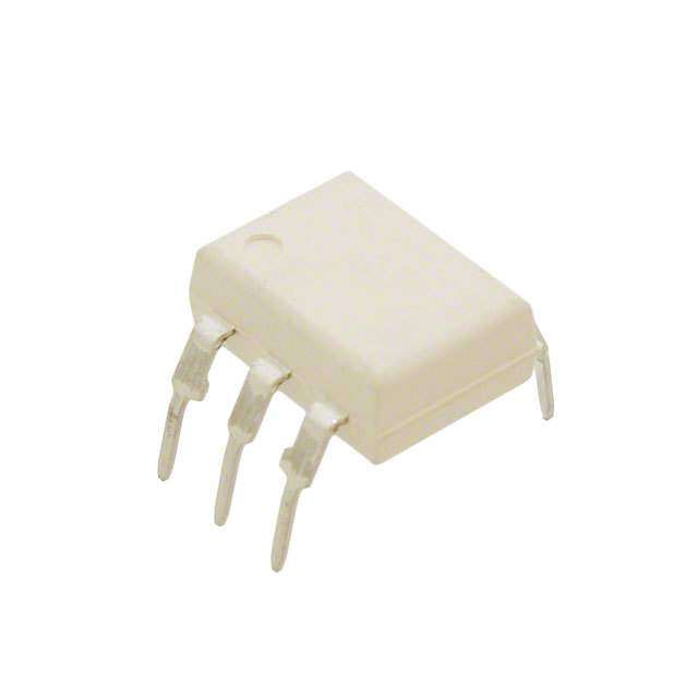
ICGOO电子元器件商城为您提供PC3SD11NTZCF由Sharp Microelectronics设计生产,在icgoo商城现货销售,并且可以通过原厂、代理商等渠道进行代购。 PC3SD11NTZCF价格参考。Sharp MicroelectronicsPC3SD11NTZCF封装/规格:光隔离器 - 三端双向可控硅,SCR输出, Optoisolator Triac Output 5000Vrms 1 Channel 6-DIP。您可以下载PC3SD11NTZCF参考资料、Datasheet数据手册功能说明书,资料中有PC3SD11NTZCF 详细功能的应用电路图电压和使用方法及教程。
| 参数 | 数值 |
| 产品目录 | |
| 描述 | OPTOCOUPLER TRIAC OUT 600V 6DIP三极与 SCR 输出光电耦合器 Phototriac non ZC 600V 5mA |
| 产品分类 | |
| 品牌 | Sharp Microelectronics |
| 产品手册 | |
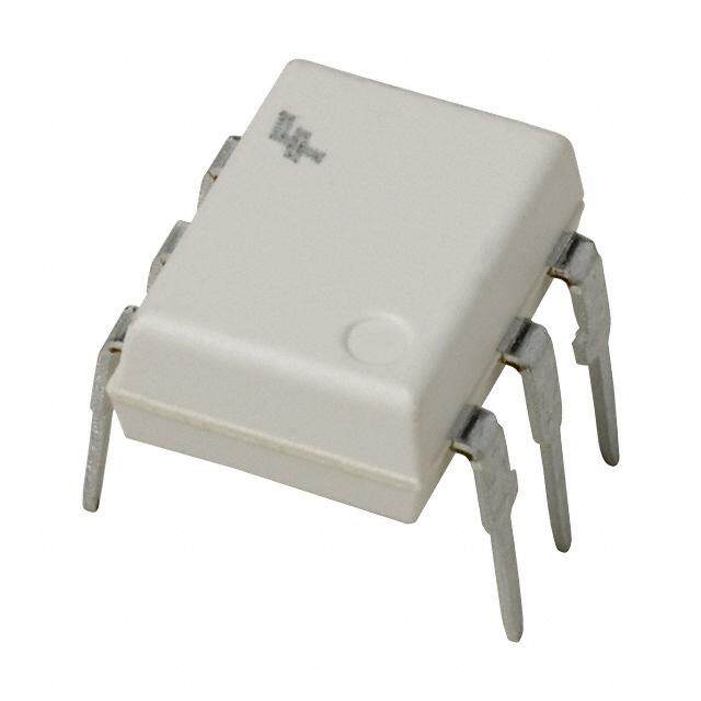
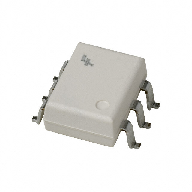
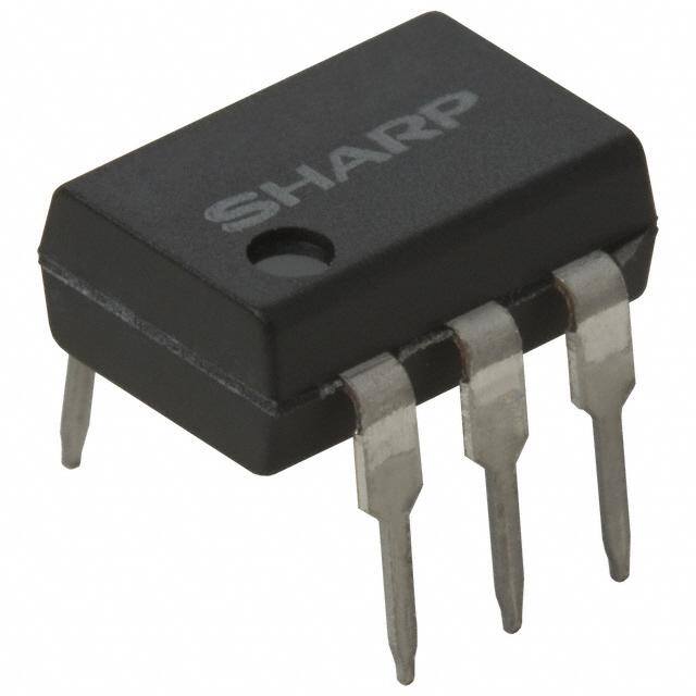
| 产品图片 |
|
| rohs | 符合RoHS无铅 / 符合限制有害物质指令(RoHS)规范要求 |
| 产品系列 | 光耦合器/光电耦合器,三极与 SCR 输出光电耦合器,Sharp Microelectronics PC3SD11NTZCF- |
| 数据手册 | http://www.sharpsma.com/webfm_send/352 |
| 产品型号 | PC3SD11NTZCF |
| 产品目录页面 | |
| 产品种类 | 三极与 SCR 输出光电耦合器 |
| 供应商器件封装 | 6-DIP |
| 关断状态下输出电压-VDRM | 600 V |
| 其它名称 | 425-2124-5 |
| 包装 | 管件 |
| 商标 | Sharp Microelectronics |
| 安装类型 | 通孔 |
| 封装/外壳 | 6-DIP(0.300",7.62mm),5 引线 |
| 封装/箱体 | PDIP-6 |
| 工厂包装数量 | 500 |
| 最大工作温度 | + 100 C |
| 最大开启时间 | 100 us |
| 最大触发电流 | 5 mA |
| 最大连续输出电流 | 100 mA |
| 最小工作温度 | - 30 C |
| 标准包装 | 50 |
| 正向电压 | 1.2 V |
| 正向电流 | 50 mA |
| 每芯片的通道数量 | 1 Channel |
| 电压-断态 | 600V |
| 电压-正向(Vf)(典型值) | 1.2V |
| 电压-隔离 | 5000Vrms |
| 电流-DC正向(If) | 50mA |
| 电流-保持(Ih) | 100µA |
| 电流-栅极触发(Igt)(最大值) | 5mA |
| 电流-输出/通道 | 100mA |
| 绝缘电压 | 5000 Vrms |
| 认可 | CSA, UR |
| 输出类型 | 交流标准三端双向可控硅开关 |
| 输出设备 | PhotoTriac |
| 通道数 | 1 |
| 零交叉电路 | Without Zero-Crossing Circuit |


.jpg)

- 商务部:美国ITC正式对集成电路等产品启动337调查
- 曝三星4nm工艺存在良率问题 高通将骁龙8 Gen1或转产台积电
- 太阳诱电将投资9.5亿元在常州建新厂生产MLCC 预计2023年完工
- 英特尔发布欧洲新工厂建设计划 深化IDM 2.0 战略
- 台积电先进制程称霸业界 有大客户加持明年业绩稳了
- 达到5530亿美元!SIA预计今年全球半导体销售额将创下新高
- 英特尔拟将自动驾驶子公司Mobileye上市 估值或超500亿美元
- 三星加码芯片和SET,合并消费电子和移动部门,撤换高东真等 CEO
- 三星电子宣布重大人事变动 还合并消费电子和移动部门
- 海关总署:前11个月进口集成电路产品价值2.52万亿元 增长14.8%
PDF Datasheet 数据手册内容提取
PC3SD11NTZ Series PC3SD11NTZ V : 600V DRM Non-zero cross type Series DIP 6pin Phototriac Coupler for triggering ∗Zero cross type is also available. (PC3SD21NTZ Series) ■ Description ■ Agency approvals/Compliance PC3SD11NTZ Series Phototriac Coupler include an 1.Recognized by UL1577 (Double protection isolation), infrared emitting diode (IRED) optically coupled to an file No. E64380 (as model No. 3SD11) output Phototriac. 2. Approved by CSA, file No. CA95323 (as model No. These devices feature full wave control and are 3SD11) ideal isolated drivers for medium to high current Triacs. 3. Optionary available VDE Approved (∗)(DIN EN 60747- DIP package provides 5.0kV isolation from input to 5-2), file No. 40008189 (as model No. 3SD11) output with superior commutative noise immunity. 4. Package resin : UL flammability grade (94V-0) (∗) DIN EN60747-5-2 : successor standard of DIN VDE0884. Up to Date code "RD" (December 2003), approval of DIN ■ Features VDE0884. From Date code "S1" (January 2004), approval of DIN 1. High repetitive peak off-state voltage (V : 600V) DRM EN60747-5-2. 2. Non-zero crossing functionality (∗∗)Reinforced insulation type is also available. 3. I ranks available (see Model Line-up section in this (PC3SF11YVZ Series) FT datasheet) 4. 6 pin DIP package ■ Applications 5. Superior noise immunity (dV/dt : MIN. 1 000V/µs) 1. Triggering for Triacs used to switch on and off 6. Lead-free components are also available (see Model devices which require AC Loads. Line-up section in this datasheet) For example heaters, fans, motors, solenoids, and 7. Double transfer mold construction (Ideal for Flow valves. Soldering) 2. Triggering for Triacs used for implementing phase 9. High isolation voltage between input and output control in applications such as lighting control and (V (rms) : 5.0kV) iso temperature control (HVAC). 3. AC line control in power supply applications. NoticeThe content of data sheet is subject to change without prior notice. In the absence of confirmation by device specification sheets, SHARP takes no responsibility for any defects that may occur in equipment using any SHARP devices shown in catalogs, data books, etc. Contact SHARP in order to obtain the latest device specification sheets before using any SHARP device. Sheet No.: D2-A07501EN 1 Date Mar. 31. 2004 © SHARP Corporation
PC3SD11NTZ Series ■ Internal Connection Diagram 1 Anode 1 6 2 Cathode 3 NC 2 5 4 Anode/Cathode 3 4 5 No external connection 6 Cathode/Anode ■ Outline Dimensions (Unit : mm) 1. Through-Hole [ex. PC3SD11NTZ] 2. Wide Through-Hole Lead-Form [ex. PC3SD11NVZ] 1.2±0.3 0.6±0.2 1.2±0.3 0.6±0.2 Model No. 6 5 4 Model No. SHARP 6 5 4 SHARP mark Rank mark mark Rank mark "S" 3SD11 "S" 3SD11 Amnaorkde 0.5±6.5 Amnaorkde 0.5±6.5 Date code (2 digit) Date code (2 digit) 1 2 3 Factory identification mark 1 3 2 Factory identification mark 7.12±0.5 7.62±0.3 7.12±0.5 7.62±0.3 0.5±2.9 0.5±3.5 TYP.0.5 Epoxy resin 0.5±2.9 0.5±3.5TYP.0.5 MIN.2.7 Epoxy resin 2.54±0.25 0.5±0.10.5±3.25 θ θ : 0 to 13˚ θ 2.54±0.25 0.5±0.10.5±3.25 10.16±0.5 0.26±0.1 Product mass : approx. 0.35g Product mass : approx. 0.35g 3. SMT Gullwing Lead-Form [ex. PC3SD11NXP] 4. Wide SMT Gullwing Lead-Form [ex. PC3SD11NWP] 0.6±0.2 1.2±0.3 0.6±0.2 1.2±0.3 6 5 4 Model No. 6 5 4 Model No. SHARP SHARP mark Rank mark mark Rank mark "S" 3SD11 "S" 3SD11 5 5 Anode 0.± Anode 0.± 5 5 mark 6. mark 6. Date code (2 digit) Date code (2 digit) 1 2 3 Factory identification mark 1 2 3Factory identification mark 5 7.12±0.5 7.62±0.3 7.12±0.5 0.±5 7.62±0.3 3. 5 0.5±3.5 0.1±0.26 0.25±0.35 1 0.2±0.25 2.54±0.25 1.0+−00.4 Epoxy resin 1.0+−00. 4 2.54±0.25 0.±0.26 Epoxy resin 10.0+−00.5 0.75±0.25 10.16±0.5 0.75±0.25 12.0MAX. Product mass : approx. 0.33g Product mass : approx. 0.34g Sheet No.: D2-A07501EN 2
PC3SD11NTZ Series ■ Outline Dimensions (Unit : mm) 5. Through-Hole VDE option [ex. PC3SD11YTZ] 6. Wide Through-Hole Lead-Form VDE option [ex. PC3SD11YVZ] 1.2±0.3 0.6±0.2 1.2±0.3 0.6±0.2 Model No. 6 5 4 Model No. SHARP 6 5 4 SHARP mark Rank mark mark Rank mark "S" 3SD11 "S" 3SD11 Amnaorkde 4 0.5±6.5 Amnaorkde 4 0.5±6.5 1 2 3 Date code (2 digit) Date code (2 digit) VDE Factory identification mark identification mark 1 2 3 VDE Factory identification mark 7.12±0.5 7.62±0.3 identification mark 0.5±2.9 0.5±3.5 TYP.0.5 7.12±0.5 0.5±3.5YP. N. 7.62±0.3 Epoxy resin 0.5±9 T0.5 MI2.7 2. 2.54±0.25 0.5±0.10.5± 5 θ θ Epoxy resin 3.2 θ : 0 to 13˚ 2.54±0.25 0.5± 10.16±0.5 0.26±0.1 5 0.5±0.1 3.2 Product mass : approx. 0.35g Product mass : approx. 0.35g 7. SMT Gullwing Lead-Form VDE option 8. Wide SMT Gullwing Lead-Form VDE option [ex. PC3SD11YXP] [ex. PC3SD11YWP] 0.6±0.2 1.2±0.3 0.6±0.2 1.2±0.3 6 5 4 Model No. 6 5 4 Model No. SHARP SHARP mark Rank mark mark Rank mark "S" 3SD11 "S" 3SD11 5 5 0. 0. Anode 4 ±5 Anode 4 ±5 mark 6. mark 6. Date code (2 digit) Date code (2 digit) 1 2 3 1 2 3 VDE Factory identification mark VDE Factory identification mark identification mark identification mark 5 7.12±0.5 7.62±0.3 7.12±0.5 0.±5 7.62±0.3 3. 5 0.5±3.5 0.1±0.26 0.25±0.35 1 0.2±0.25 2.54±0.25 1.0+−00.4 Epoxy resin 1.0+−00. 4 2.54±0.25 0.±0.26 Epoxy resin 10.0+−00.5 0.75±0.25 10.16±0.5 0.75±0.25 12.0MAX. Product mass : approx. 0.33g Product mass : approx. 0.34g ∗Pin 5 is not allowed external connection Sheet No.: D2-A07501EN 3
PC3SD11NTZ Series Date code (2 digit) 1st digit 2nd digit Year of production Month of production A.D. Mark A.D Mark Month Mark 1990 A 2002 P January 1 1991 B 2003 R February 2 1992 C 2004 S March 3 1993 D 2005 T April 4 1994 E 2006 U May 5 1995 F 2007 V June 6 1996 H 2008 W July 7 1997 J 2009 X August 8 1998 K 2010 A September 9 1999 L 2011 B October O 2000 M 2012 C November N · · 2001 N ·· ·· December D repeats in a 20 year cycle Factory identification mark Factory identification Mark Country of origin no mark Japan Indonesia Philippines China * This factory marking is for identification purpose only. Please contact the local SHARP sales representative to see the actural status of the production. Rank mark Refer to the Model Line-up table Sheet No.: D2-A07501EN 4
PC3SD11NTZ Series ■ Absolute Maximum Ratings (T=25˚C) a Parameter Symbol Rating Unit Forward current I 50 mA F Input Reverse voltage V 6 V R RMS ON-state current I (rms) 0.1 A T Output Peak one cycle surge current I 1.2*3 A surge m Repetitive peak OFF-state voltage V 600 V m DRM 1 *1 Isolation voltage V (rms) 5.0 kV iso Operating temperature T −30 to +100 ˚C opr Storage temperature Tstg −55 to +125 ˚C Soldering area *2 Soldering temperature Tsol 270*4 ˚C *1 40 to 60%RH, AC for 1minute, f=60Hz *2 For 10s *3 f=50Hz sine wave *4 Lead solder plating models: 260˚C ■ Electro-optical Characteristics (T=25˚C) a Parameter Symbol Conditions MIN. TYP. MAX. Unit Forward voltage VF IF=20mA − 1.2 1.4 V Input Reverse current IR VR=3V − − 10 µA Repentitive peak OFF-state current IDRM VD=VDRM − − 1 µA ON-state voltage VT IT=0.1A − − 2.5 V Output Holding current IH VD=6V 0.1 − 3.5 mA − Critical rate of rise of OFF-state voltage dV/dt VD=1/√2 ·VDRM 1 000 2 000 − V/µs Rank A − − 10 Transfer Minimum trigger current Rank B IFT VD=6V, RL=100Ω − − 7 mA charac- Rank C − − 5 teristics Isolation resistance RISO DC500V,40 to 60%RH 5×10¹⁰ 1011 − Ω Turn-on time ton VD=6V, RL=100Ω, IF=20mA − − 100 µs Sheet No.: D2-A07501EN 5
PC3SD11NTZ Series ■ Model Line-up (1) (Lead-free components) Lead Form Through-Hole SMT Gullwing Wide Through-Hole Sleeve I [mA] Shipping Package FT 50pcs/sleeve Rank mark (V =6V, D DIN RL=100Ω) - Approved - Approved - Approved EN60747-5-2 PC3SD11NTZAF PC3SD11YTZAF PC3SD11NXZAF PC3SD11YXZAF PC3SD11NVZAF PC3SD11YVZAF A MAX.10 Model No. PC3SD11NTZBF PC3SD11YTZBF PC3SD11NXZBF PC3SD11YXZBF PC3SD11NVZBF PC3SD11YVZBF B MAX.7 PC3SD11NTZCF PC3SD11YTZCF PC3SD11NXZCF PC3SD11YXZCF PC3SD11NVZCF PC3SD11YVZCF C MAX.5 Lead Form Wide SMT Gullwing SMT Gullwing Wide SMT Gullwing Sleeve Taping I [mA] Shipping Package FT 50pcs/sleeve 1 000pcs/reel Rank mark (V =6V, D DIN RL=100Ω) - Approved - Approved - Approved EN60747-5-2 PC3SD11NWZAF PC3SD11YWZAF PC3SD11NXPAF PC3SD11YXPAF PC3SD11NWPAF PC3SD11YWPAF A MAX.10 Model No. PC3SD11NWZBF PC3SD11YWZBF PC3SD11NXPBF PC3SD11YXPBF PC3SD11NWPBF PC3SD11YWPBF B MAX.7 PC3SD11NWZCF PC3SD11YWZCF PC3SD11NXPCF PC3SD11YXPCF PC3SD11NWPCF PC3SD11YWPCF C MAX.5 ■ Model Line-up (2) (Lead solder plating components) Lead Form Through-Hole SMT Gullwing Wide Through-Hole Sleeve I [mA] Shipping Package FT 50pcs/sleeve Rank mark (V =6V, D DIN RL=100Ω) - Approved - Approved - Approved EN60747-5-2 PC3SD11NTZA PC3SD11YTZA PC3SD11NXZA PC3SD11YXZA PC3SD11NVZA PC3SD11YVZA A MAX.10 Model No. PC3SD11NTZB PC3SD11YTZB PC3SD11NXZB PC3SD11YXZB PC3SD11NVZB PC3SD11YVZB B MAX.7 PC3SD11NTZC PC3SD11YTZC PC3SD11NXZC PC3SD11YXZC PC3SD11NVZC PC3SD11YVZC C MAX.5 Lead Form Wide SMT Gullwing SMT Gullwing Wide SMT Gullwing Sleeve Taping I [mA] Shipping Package FT 50pcs/sleeve 1 000pcs/reel Rank mark (V =6V, D DIN RL=100Ω) - Approved - Approved - Approved EN60747-5-2 PC3SD11NWZA PC3SD11YWZA PC3SD11NXPA PC3SD11YXPA PC3SD11NWPA PC3SD11YWPA A MAX.10 Model No. PC3SD11NWZB PC3SD11YWZB PC3SD11NXPB PC3SD11YXPB PC3SD11NWPB PC3SD11YWPB B MAX.7 PC3SD11NWZC PC3SD11YWZC PC3SD11NXPC PC3SD11YXPC PC3SD11NWPC PC3SD11YWPC C MAX.5 Please contact a local SHARP sales representative to inquire about production status. Sheet No.: D2-A07501EN 6
PC3SD11NTZ Series Fig.1 Forward Current vs. Ambient Fig.2 RMS ON-state Current vs. Temperature Ambient Temperature 70 175 60 A) 150 m A) 50 ms) ( 125 Forward current I (mF 234000 ON-state current I(rr 1570050 S M 10 R 25 0 0 −30 0 50 100 −30 0 50 100 Ambient temperature Ta (˚C) Ambient temperature Ta (˚C) Fig.3-a Forward Current vs. Forward Voltage Fig.3-b Forward Current vs. Forward Voltage (Rank A) (Rank B, Rank C) 100 100 Ta=75˚C mA) 50 Ta=17050°°CC mA) 50 50˚C (F 50°C (F ent I 25°C ent I 25˚C 0˚C urr 0°C urr c 10 c 10 d d ar −30°C ar w w For 5 For 5 −25˚C 1 1 0 0.5 1 1.5 2 2.5 3 0.9 1 1.1 1.2 1.3 1.4 1.5 Forward voltage VF (V) Forward voltage VF (V) Fig.4-a Minimum Trigger Current vs. Ambient Fig.4-b Minimum Trigger Current vs. Ambient Temperature (Rank A) Temperature (Rank B, Rank C) 10 10 VD=6V VD=6V RL=100Ω RL=100Ω A) 8 A) 8 m m m trigger current I (FT 46 m trigger current I (FT 46 mu mu Mini 2 Mini 2 0 0 −40 −20 0 20 40 60 80 100 −40 −20 0 20 40 60 80 100 Ambient temperature Ta (˚C) Ambient temperature Ta (˚C) Sheet No.: D2-A07501EN 7
PC3SD11NTZ Series Fig.5 Relative Repetitive Peak OFF-state Fig.6 ON-state Voltage vs. Voltage vs. Ambient Temperature Ambient Temperature 1.3 I=100mA 2.4 T e g oltaC) 1.2 2.2 elative repetitive peak OFF-state vV (TT) / V (T25˚==DRMjaDRMj 001...8911 ON-state voltage V (V)T 1111....24682 R 0.7 1 −40 −20 0 20 40 60 80 100 −40 −20 0 20 40 60 80 100 Ambient temperature Ta (˚C) Ambient temperature Ta (˚C) Fig.7 Holding Current vs. Fig.8 Repetitive Peak OFF-state Current vs. Ambient Temperature Ambient Temperature 10 10−6 VD=6V (A)M VD=600V R A) nt ID 10−7 m e urrent I (H 1 F-state curr 10−8 g c OF Holdin e peak 10−9 v etiti p e R 0.1 10−10 −40 −20 0 20 40 60 80 100 −40 −20 0 20 40 60 80 100 Ambient temperature Ta (˚C) Ambient temperature Ta (˚C) Fig.9-a Turn-on Time vs. Forward Current Fig.9-b Turn-on Time vs. Forward Current (Rank A) (Rank B, Rank C) 1 000 1 000 VD=6V VD=6V RL=100Ω RL=100Ω Ta=25˚C Ta=25˚C me t (s)µON 100 me t (s)µON 100 Turn-on ti Turn-on ti 10 10 1 10 100 1 10 100 Forward current IF (mA) Forward current IF (mA) Remarks : Please be aware that all data in the graph are just for reference. Sheet No.: D2-A07501EN 8
PC3SD11NTZ Series ■ Design Considerations ● Design guide In order for the Phototriac to turn off, the triggering current (I ) must be 0.1mA or less. F Please refrain from using these devices in a direct drive configuration. These Phototriac Coupler are intended to be used as triggering device for main Triacs. Please ensure that the output rating of these devices will be sufficient for triggering the main output Triac of your choice. Failure to do may result in malfunctions. In phase control applications or where the Phototriac Coupler is being by a pulse signal, please ensure that the pulse width is a minimum of 1ms. For designs that will experience excessive noise or sudden changes in load voltage, please include an appropriate snubber circuit as shown in the below circuit. Please keep in mind that Sharp Phototriac Couplers incorporate superor dV/dt ratings which can often eliminate the need for a snubber circuit. ● Degradation In general, the emission of the IRED used in Phototriac Couplers will degrade over time. In the case where long term operation and / or constant extreme temperature fluctuations will be applied to the devices, please allow for a worst case scenario of 50% degradation over 5years. Therefore in order to maintain proper operation, a design implementing these Phototriac Couplers should provide at least twice the minimum required triggering current from initial operation. ● Recommended Foot Print (reference) SMT Gullwing Lead-form Wide SMT Gullwing Lead-form 8.2 10.2 4 4 5 5 2. 2. 4 4 5 5 2. 2. 7 7 1. 1. 2.2 2.2 (Unit : mm) Sheet No.: D2-A07501EN 9
PC3SD11NTZ Series ● Standard Circuit (Medium/High Power Triac Drive Circuit) PC3SD11NTZ 1 6 Load 5 AC Line 2 Triac 3 4 Note) Please add the snubber circuit according to a condition. Any snubber or varistor used for the above mentioned scenarios should be located as close to the main output triac as possible. ✩ For additional design assistance, please review our corresponding Optoelectronic Application Notes. Sheet No.: D2-A07501EN 10
PC3SD11NTZ Series ■ Manufacturing Guidelines ● Soldering Method Reflow Soldering: Reflow soldering should follow the temperature profile shown below. Soldering should not exceed the curve of temperature profile and time. Please don't solder more than twice. (˚C) 300 Terminal : 260˚C peak ( package surface : 250˚C peak) 200 Reflow 220˚C or more, 60s or less Preheat 100 150 to 180˚C, 120s or less 0 0 1 2 3 4 (min) Flow Soldering : Due to SHARP's double transfer mold construction submersion in flow solder bath is allowed under the below listed guidelines. Flow soldering should be completed below 270˚C and within 10s. Preheating is within the bounds of 100 to 150˚C and 30 to 80s. Please don't solder more than twice. Hand soldering Hand soldering should be completed within 3s when the point of solder iron is below 400˚C. Please don't solder more than twice. Other notices Please test the soldering method in actual condition and make sure the soldering works fine, since the impact on the junction between the device and PCB varies depending on the tooling and soldering conditions. Sheet No.: D2-A07501EN 11
PC3SD11NTZ Series ● Cleaning instructions Solvent cleaning : Solvent temperature should be 45˚C or below. Immersion time should be 3minutes or less. Ultrasonic cleaning : The impact on the device varies depending on the size of the cleaning bath, ultrasonic output, cleaning time, size of PCB and mounting method of the device. Therefore, please make sure the device withstands the ultrasonic cleaning in actual conditions in advance of mass production. Recommended solvent materials : Ethyl alcohol, Methyl alcohol and Isopropyl alcohol. In case the other type of solvent materials are intended to be used, please make sure they work fine in actual using conditions since some materials may erode the packaging resin. ● Presence of ODC This product shall not contain the following materials. And they are not used in the production process for this device. Regulation substances : CFCs, Halon, Carbon tetrachloride, 1.1.1-Trichloroethane (Methylchloroform) Specific brominated flame retardants such as the PBBOs and PBBs are not used in this product at all. Sheet No.: D2-A07501EN 12
PC3SD11NTZ Series ■ Package specification ● Sleeve package 1. Through-Hole or SMT Gullwing Package materials Sleeve : HIPS (with anti-static material) Stopper : Styrene-Elastomer Package method MAX. 50pcs of products shall be packaged in a sleeve. Both ends shall be closed by tabbed and tabless stoppers. The product shall be arranged in the sleeve with its anode mark on the tabless stopper side. MAX. 20 sleeves in one case. Sleeve outline dimensions 12.0 520±2 8 0. 1 8 5. 6.7 (Unit : mm) 2. Wide Through-Hole or Wide SMT Gullwing Package materials Sleeve : HIPS (with anti-static material) Stopper : Styrene-Elastomer Package method MAX. 50pcs of products shall be packaged in a sleeve. Both ends shall be closed by tabbed and tabless stoppers. The product shall be arranged in the sleeve with its anode mark on the tabless stopper side. MAX. 20 sleeves in one case. Sleeve outline dimensions 15.0 520±2 8 0. 1 9 5. 6.35 (Unit : mm) Sheet No.: D2-A07501EN 13
PC3SD11NTZ Series ● Tape and Reel package 1. SMT Gullwing Package materials Carrier tape : A-PET (with anti-static material) Cover tape : PET (three layer system) Reel : PS Carrier tape structure and Dimensions F D G J I E C B A H H .X A M K ˚5 Dimensions List (Unit:mm) A B C D E F G 16.0±0.3 7.5±0.1 1.75±0.1 12.0±0.1 2.0±0.1 4.0±0.1 φ1.5+0.1 −0 H I J K 10.4±0.1 0.4±0.05 4.2±0.1 7.8±0.1 Reel structure and Dimensions e d g c Dimensions List (Unit : mm) a b c d 330 17.5±1.5 100±1.0 13±0.5 f e f g a b 23±1.0 2.0±0.5 2.0±0.5 Direction of product insertion Pull-out direction [Packing : 1 000pcs/reel] Sheet No.: D2-A07501EN 14
PC3SD11NTZ Series 2. Wide SMT Gullwing Package materials Carrier tape : A-PET (with anti-static material) Cover tape : PET (three layer system) Reel : PS Carrier tape structure and Dimensions F D G J I E C B A H H .X K AM˚5 Dimensions List (Unit : mm) A B C D E F G 24.0±0.3 11.5±0.1 1.75±0.1 12.0±0.1 2.0±0.1 4.0±0.1 φ1.5+0.1 −0 H I J K 12.2±0.1 0.4±0.05 4.15±0.1 7.6±0.1 Reel structure and Dimensions e d g c Dimensions List (Unit : mm) a b c d 330 25.5±1.5 100±1.0 13±0.5 e f g f a b 23±1.0 2.0±0.5 2.0±0.5 Direction of product insertion Pull-out direction [Packing : 1 000pcs/reel] Sheet No.: D2-A07501EN 15
PC3SD11NTZ Series ■ Important Notices · The circuit application examples in this publication are with equipment that requires higher reliability such as: provided to explain representative applications of --- Transportation control and safety equipment (i.e., SHARP devices and are not intended to guarantee any aircraft, trains, automobiles, etc.) circuit design or license any intellectual property rights. --- Traffic signals SHARP takes no responsibility for any problems rela- --- Gas leakage sensor breakers ted to any intellectual property right of a third party re- --- Alarm equipment sulting from the use of SHARP's devices. --- Various safety devices, etc. (iii) SHARP devices shall not be used for or in connec- · Contact SHARP in order to obtain the latest device tion with equipment that requires an extremely high lev- specification sheets before using any SHARP device. el of reliability and safety such as: SHARP reserves the right to make changes in the spec- --- Space applications ifications, characteristics, data, materials, structure, --- Telecommunication equipment [trunk lines] and other contents described herein at any time without --- Nuclear power control equipment notice in order to improve design or reliability. Manufac- --- Medical and other life support equipment (e.g., turing locations are also subject to change without no- scuba). tice. · If the SHARP devices listed in this publication fall with- · Observe the following points when using any devices in the scope of strategic products described in the For- in this publication. SHARP takes no responsibility for eign Exchange and Foreign Trade Law of Japan, it is damage caused by improper use of the devices which necessary to obtain approval to export such SHARP de- does not meet the conditions and absolute maximum vices. ratings to be used specified in the relevant specification sheet nor meet the following conditions: · This publication is the proprietary product of SHARP (i) The devices in this publication are designed for use and is copyrighted, with all rights reserved. Under the in general electronic equipment designs such as: copyright laws, no part of this publication may be repro- --- Personal computers duced or transmitted in any form or by any means, elec- --- Office automation equipment tronic or mechanical, for any purpose, in whole or in --- Telecommunication equipment [terminal] part, without the express written permission of SHARP. --- Test and measurement equipment Express written permission is also required before any --- Industrial control use of this publication may be made by a third party. --- Audio visual equipment --- Consumer electronics · Contact and consult with a SHARP representative if (ii) Measures such as fail-safe function and redundant there are any questions about the contents of this pub- design should be taken to ensure reliability and safety lication. when SHARP devices are used for or in connection Sheet No.: D2-A07501EN 16
 Datasheet下载

