ICGOO在线商城 > 分立半导体产品 > 晶体管 - 双极 (BJT) - 单 > PBSS303PD,115
 Datasheet下载
- 型号: PBSS303PD,115
- 制造商: NXP Semiconductors
- 库位|库存: xxxx|xxxx
- 要求:
| 数量阶梯 | 香港交货 | 国内含税 |
| +xxxx | $xxxx | ¥xxxx |
查看当月历史价格
查看今年历史价格
PBSS303PD,115产品简介:
ICGOO电子元器件商城为您提供PBSS303PD,115由NXP Semiconductors设计生产,在icgoo商城现货销售,并且可以通过原厂、代理商等渠道进行代购。 PBSS303PD,115价格参考。NXP SemiconductorsPBSS303PD,115封装/规格:晶体管 - 双极 (BJT) - 单, 双极 (BJT) 晶体管 PNP 60V 1A 110MHz 1.1W 表面贴装 6-TSOP。您可以下载PBSS303PD,115参考资料、Datasheet数据手册功能说明书,资料中有PBSS303PD,115 详细功能的应用电路图电压和使用方法及教程。
| 参数 | 数值 |
| 产品目录 | |
| 描述 | TRANS PNP 60V 3A 6TSOP两极晶体管 - BJT TRANS BISS TAPE-7 |
| 产品分类 | 晶体管(BJT) - 单路分离式半导体 |
| 品牌 | NXP Semiconductors |
| 产品手册 | |
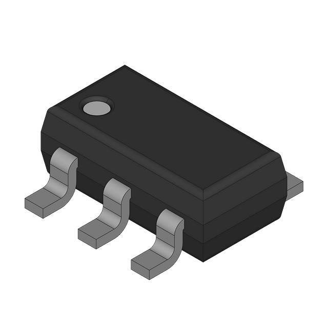
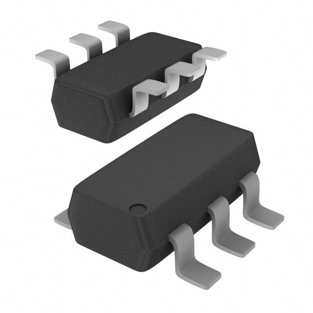
| 产品图片 |
|
| rohs | 符合RoHS无铅 / 符合限制有害物质指令(RoHS)规范要求 |
| 产品系列 | 晶体管,两极晶体管 - BJT,NXP Semiconductors PBSS303PD,115- |
| 数据手册 | |
| 产品型号 | PBSS303PD,115 |
| PCN封装 | |
| 不同 Ib、Ic时的 Vce饱和值(最大值) | 675mV @ 600mA,6A |
| 不同 Ic、Vce 时的DC电流增益(hFE)(最小值) | 180 @ 500mA,2V |
| 产品种类 | 两极晶体管 - BJT |
| 供应商器件封装 | 6-TSOP |
| 其它名称 | 568-7273-1 |
| 功率-最大值 | 1.1W |
| 包装 | 剪切带 (CT) |
| 发射极-基极电压VEBO | 5 V |
| 商标 | NXP Semiconductors |
| 增益带宽产品fT | 110 MHz |
| 安装类型 | 表面贴装 |
| 安装风格 | SMD/SMT |
| 封装 | Reel |
| 封装/外壳 | SC-74,SOT-457 |
| 封装/箱体 | TSOP |
| 工厂包装数量 | 3000 |
| 晶体管极性 | PNP |
| 晶体管类型 | PNP |
| 最大功率耗散 | 2500 mW |
| 最大工作温度 | + 150 C |
| 最大直流电集电极电流 | 3 A |
| 最小工作温度 | - 65 C |
| 标准包装 | 1 |
| 特色产品 | http://www.digikey.com/cn/zh/ph/NXP/I2C.html |
| 电压-集射极击穿(最大值) | 60V |
| 电流-集电极(Ic)(最大值) | 1A |
| 电流-集电极截止(最大值) | 100nA |
| 直流电流增益hFE最大值 | 180 at 500 mA at 2 V |
| 直流集电极/BaseGainhfeMin | 180 at 500 mA at 2 V, 160 at 1 A at 2 V, 130 at 2 A at 2 V, 95 at 3 A at 2 V, 60 at 4 A at 2 V, 35 at 5 A at 2 V, 20 at 6 A at 2 V |
| 配置 | Single |
| 集电极—发射极最大电压VCEO | 60 V |
| 集电极—基极电压VCBO | 60 V |
| 零件号别名 | PBSS303PD T/R |
| 频率-跃迁 | 110MHz |


- 商务部:美国ITC正式对集成电路等产品启动337调查
- 曝三星4nm工艺存在良率问题 高通将骁龙8 Gen1或转产台积电
- 太阳诱电将投资9.5亿元在常州建新厂生产MLCC 预计2023年完工
- 英特尔发布欧洲新工厂建设计划 深化IDM 2.0 战略
- 台积电先进制程称霸业界 有大客户加持明年业绩稳了
- 达到5530亿美元!SIA预计今年全球半导体销售额将创下新高
- 英特尔拟将自动驾驶子公司Mobileye上市 估值或超500亿美元
- 三星加码芯片和SET,合并消费电子和移动部门,撤换高东真等 CEO
- 三星电子宣布重大人事变动 还合并消费电子和移动部门
- 海关总署:前11个月进口集成电路产品价值2.52万亿元 增长14.8%


PDF Datasheet 数据手册内容提取
Important notice Dear Customer, On 7 February 2017 the former NXP Standard Product business became a new company with the tradename Nexperia. Nexperia is an industry leading supplier of Discrete, Logic and PowerMOS semiconductors with its focus on the automotive, industrial, computing, consumer and wearable application markets In data sheets and application notes which still contain NXP or Philips Semiconductors references, use the references to Nexperia, as shown below. Instead of http://www.nxp.com, http://www.philips.com/ or http://www.semiconductors.philips.com/, use http://www.nexperia.com Instead of sales.addresses@www.nxp.com or sales.addresses@www.semiconductors.philips.com, use salesaddresses@nexperia.com (email) Replace the copyright notice at the bottom of each page or elsewhere in the document, depending on the version, as shown below: - © NXP N.V. (year). All rights reserved or © Koninklijke Philips Electronics N.V. (year). All rights reserved Should be replaced with: - © Nexperia B.V. (year). All rights reserved. If you have any questions related to the data sheet, please contact our nearest sales office via e-mail or telephone (details via salesaddresses@nexperia.com). Thank you for your cooperation and understanding, Kind regards, Team Nexperia
PBSS303PD 60 V, 3 A PNP low V (BISS) transistor CEsat Rev. 02 — 20 November 2009 Product data sheet 1. Product profile 1.1 General description PNP low V Breakthrough In Small Signal (BISS) transistor in a SOT457 (SC-74) CEsat small Surface-Mounted Device (SMD) plastic package. NPN complement: PBSS303ND. 1.2 Features (cid:132) Low collector-emitter saturation voltage V CEsat (cid:132) High collector current capability I and I C CM (cid:132) High collector current gain (h ) at high I FE C (cid:132) High efficiency due to less heat generation (cid:132) Smaller required Printed-Circuit Board (PCB) area than for conventional transistors 1.3 Applications (cid:132) High-voltage DC-to-DC conversion (cid:132) High-voltage MOSFET gate driving (cid:132) High-voltage motor control (cid:132) High-voltage power switches (e.g. motors, fans) (cid:132) Thin Film Transistor (TFT) backlight inverter (cid:132) Automotive applications 1.4 Quick reference data Table 1. Quick reference data Symbol Parameter Conditions Min Typ Max Unit V collector-emitter voltage open base - - −60 V CEO I collector current [1] - - −3 A C I peak collector current single pulse; - - −6 A CM t ≤1ms p R collector-emitter I =−2A; [2] - 75 100 mΩ CEsat C saturation resistance I =−200mA B [1] Device mounted on a ceramic PCB, Al O , standard footprint. 2 3 [2] Pulse test: tp≤300μs; δ≤0.02.
PBSS303PD NXP Semiconductors 60 V, 3 A PNP low V (BISS) transistor CEsat 2. Pinning information Table 2. Pinning Pin Description Simplified outline Symbol 1 collector 6 5 4 1, 2, 5, 6 2 collector 3 base 3 4 emitter 1 2 3 4 5 collector sym030 6 collector 3. Ordering information Table 3. Ordering information Type number Package Name Description Version PBSS303PD SC-74 plastic surface-mounted package (TSOP6); 6leads SOT457 4. Marking Table 4. Marking codes Type number Marking code PBSS303PD AH PBSS303PD_2 © NXP B.V. 2009. All rights reserved. Product data sheet Rev. 02 — 20 November 2009 2 of 16
PBSS303PD NXP Semiconductors 60 V, 3 A PNP low V (BISS) transistor CEsat 5. Limiting values Table 5. Limiting values In accordance with the Absolute Maximum Rating System (IEC 60134). Symbol Parameter Conditions Min Max Unit V collector-base voltage open emitter - −60 V CBO V collector-emitter voltage open base - −60 V CEO V emitter-base voltage open collector - −5 V EBO I collector current [1] - −1 A C [2] - −3 A I peak collector current single pulse; - −6 A CM t ≤1ms p I base current - −800 mA B I peak base current single pulse; - −2 A BM t ≤1ms p P total power dissipation T ≤25°C [1] - 360 mW tot amb [3] - 600 mW [4] - 750 mW [2] - 1.1 W [1][5] - 2.5 W T junction temperature - 150 °C j T ambient temperature −65 +150 °C amb T storage temperature −65 +150 °C stg [1] Device mounted on an FR4PCB, single-sided copper, tin-plated and standard footprint. [2] Device mounted on a ceramic PCB, Al O , standard footprint. 2 3 [3] Device mounted on an FR4PCB, single-sided copper, tin-plated, mounting pad for collector 1cm2. [4] Device mounted on an FR4PCB, single-sided copper, tin-plated, mounting pad for collector 6cm2. [5] Pulse test: tp≤10ms; δ≤10%. PBSS303PD_2 © NXP B.V. 2009. All rights reserved. Product data sheet Rev. 02 — 20 November 2009 3 of 16
PBSS303PD NXP Semiconductors 60 V, 3 A PNP low V (BISS) transistor CEsat 006aaa270 1600 Ptot (mW) 1200 (1) 800 (2) (3) 400 (4) 0 −75 −25 25 75 125 175 Tamb (°C) (1) Ceramic PCB, Al O , standard footprint 2 3 (2) FR4PCB, mounting pad for collector 6cm2 (3) FR4PCB, mounting pad for collector 1cm2 (4) FR4PCB, standard footprint Fig 1. Power derating curves 6. Thermal characteristics Table 6. Thermal characteristics Symbol Parameter Conditions Min Typ Max Unit R thermal resistance from in free air [1] - - 350 K/W th(j-a) junction to ambient [2] - - 208 K/W [3] - - 167 K/W [4] - - 113 K/W [1][5] - - 50 K/W R thermal resistance from - - 45 K/W th(j-sp) junction to solder point [1] Device mounted on an FR4PCB, single-sided copper, tin-plated and standard footprint. [2] Device mounted on an FR4PCB, single-sided copper, tin-plated, mounting pad for collector 1cm2. [3] Device mounted on an FR4PCB, single-sided copper, tin-plated, mounting pad for collector 6cm2. [4] Device mounted on a ceramic PCB, Al O , standard footprint. 2 3 [5] Pulse test: tp≤10ms; δ≤10%. PBSS303PD_2 © NXP B.V. 2009. All rights reserved. Product data sheet Rev. 02 — 20 November 2009 4 of 16
PBSS303PD NXP Semiconductors 60 V, 3 A PNP low V (BISS) transistor CEsat 103 006aaa271 Zth(j-a) duty cycle = 1 (K/W) 0.75 0.5 102 0.33 0.2 0.1 0.05 10 0.02 0.01 1 0 10−1 10−5 10−4 10−3 10−2 10−1 1 10 102 103 tp (s) FR4PCB, standard footprint Fig 2. Transient thermal impedance from junction to ambient as a function of pulse duration; typical values 103 006aaa272 Zth(j-a) duty cycle = (K/W) 1 0.75 102 0.5 0.33 0.2 0.1 10 0.05 0.02 0.01 1 0 10−1 10−5 10−4 10−3 10−2 10−1 1 10 102 103 tp (s) FR4PCB, mounting pad for collector 1cm2 Fig 3. Transient thermal impedance from junction to ambient as a function of pulse duration; typical values PBSS303PD_2 © NXP B.V. 2009. All rights reserved. Product data sheet Rev. 02 — 20 November 2009 5 of 16
PBSS303PD NXP Semiconductors 60 V, 3 A PNP low V (BISS) transistor CEsat 103 006aaa273 Zth(j-a) (K/W) duty cycle = 1 102 0.75 0.5 0.33 0.2 0.1 10 0.05 0.02 0.01 1 0 10−1 10−5 10−4 10−3 10−2 10−1 1 10 102 103 tp (s) FR4PCB, mounting pad for collector 6cm2 Fig 4. Transient thermal impedance from junction to ambient as a function of pulse duration; typical values 103 006aaa751 Zth(j-a) (K/W) duty cycle = 102 1 0.75 0.5 0.33 0.2 10 0.1 0.05 0.02 0.01 1 0 10−1 10−5 10−4 10−3 10−2 10−1 1 10 102 103 tp (s) Ceramic PCB, Al O , standard footprint 2 3 Fig 5. Transient thermal impedance from junction to ambient as a function of pulse duration; typical values PBSS303PD_2 © NXP B.V. 2009. All rights reserved. Product data sheet Rev. 02 — 20 November 2009 6 of 16
PBSS303PD NXP Semiconductors 60 V, 3 A PNP low V (BISS) transistor CEsat 7. Characteristics Table 7. Characteristics T =25°C unless otherwise specified. amb Symbol Parameter Conditions Min Typ Max Unit I collector-base cut-off V =−60V; I =0A - - −100 nA CBO CB E current V =−60V; I =0A; - - −50 μA CB E T =150°C j I collector-emitter V =−48V; V =0V - - −100 nA CES CE BE cut-off current I emitter-base cut-off V =−5V; I =0A - - −100 nA EBO EB C current h DCcurrent gain V =−2V; I =−500mA 180 265 - FE CE C V =−2V; I =−1A [1] 160 235 - CE C V =−2V; I =−2A [1] 130 185 - CE C V =−2V; I =−3A [1] 95 135 - CE C V =−2V; I =−4A [1] 60 80 - CE C V =−2V; I =−5A [1] 35 50 - CE C V =−2V; I =−6A [1] 20 30 - CE C V collector-emitter I =−500mA; I =−50mA - −55 −70 mV CEsat C B saturation voltage I =−1A; I =−50mA - −100 −135 mV C B I =−2A; I =−200mA [1] - −150 −200 mV C B I =−3A; I =−150mA [1] - −275 −365 mV C B I =−3A; I =−300mA [1] - −210 −290 mV C B I =−4A; I =−400mA [1] - −285 −385 mV C B I =−5A; I =−500mA [1] - −375 −495 mV C B I =−6A; I =−600mA [1] - −515 −675 mV C B R collector-emitter I =−2A; I =−200mA [1] - 75 100 mΩ CEsat C B saturation resistance V base-emitter I =−500mA; I =−50mA - −0.78 −0.87 V BEsat C B saturation voltage I =−1A; I =−50mA - −0.80 −0.89 V C B I =−1A; I =−100mA [1] - −0.83 −0.92 V C B I =−3A; I =−150mA [1] - −0.92 −0.99 V C B I =−3A; I =−300mA [1] - −0.94 −1.02 V C B V base-emitter turn-on V =−2V; I =−2A - −0.80 −1.00 V BEon CE C voltage PBSS303PD_2 © NXP B.V. 2009. All rights reserved. Product data sheet Rev. 02 — 20 November 2009 7 of 16
PBSS303PD NXP Semiconductors 60 V, 3 A PNP low V (BISS) transistor CEsat Table 7. Characteristics …continued T =25°C unless otherwise specified. amb Symbol Parameter Conditions Min Typ Max Unit t delay time V =−9.2V; I =−2A; - 13 - ns d CC C I =−0.1A; I =0.1A t rise time Bon Boff - 53 - ns r t turn-on time - 66 - ns on t storage time - 230 - ns s t fall time - 76 - ns f t turn-off time - 306 - ns off f transition frequency V =−10V; I =−100mA; - 110 - MHz T CE C f=100MHz C collector capacitance V =−10V; I =i =0A; - 58 - pF c CB E e f=1MHz [1] Pulse test: tp≤300μs; δ≤0.02. PBSS303PD_2 © NXP B.V. 2009. All rights reserved. Product data sheet Rev. 02 — 20 November 2009 8 of 16
PBSS303PD NXP Semiconductors 60 V, 3 A PNP low V (BISS) transistor CEsat 600 006aaa727 −6 006aaa728 IB = −190 mA −171 hFE IC −152 (A) −133 −114 (1) −95 −57 400 −4 −76 −38 (2) −19 200 −2 (3) 0 0 −10−1 −1 −10 −102 −103 −104 0 −0.4 −0.8 −1.2 −1.6 −2.0 IC (mA) VCE (V) VCE=−2V Tamb=25°C (1) Tamb=100°C (2) Tamb=25°C (3) Tamb=−55°C Fig 6. DCcurrent gain as a function of collector Fig 7. Collector current as a function of current; typical values collector-emitter voltage; typical values −1.2 006aaa729 −1.2 006aaa730 VBE VBEsat (V) (V) −0.8 (1) −0.8 (1) (2) (2) −0.4 (3) −0.4 (3) 0 0 −10−1 −1 −10 −102 −103 −104 −10−1 −1 −10 −102 −103 −104 IC (mA) IC (mA) VCE=−2V IC/IB=20 (1) Tamb=−55°C (1) Tamb=−55°C (2) Tamb=25°C (2) Tamb=25°C (3) Tamb=100°C (3) Tamb=100°C Fig 8. Base-emitter voltage as a function of collector Fig 9. Base-emitter saturation voltage as a function current; typical values of collector current; typical values PBSS303PD_2 © NXP B.V. 2009. All rights reserved. Product data sheet Rev. 02 — 20 November 2009 9 of 16
PBSS303PD NXP Semiconductors 60 V, 3 A PNP low V (BISS) transistor CEsat −1 006aaa731 −1 006aaa732 VCEsat (V) VCEsat (V) −10−1 (1) (1) (2) (2) −10−1 (3) (3) −10−2 −10−2 −10−3 −10−1 −1 −10 −102 −103 −104 −10−1 −1 −10 −102 −103 −104 IC (mA) IC (mA) IC/IB=20 Tamb=25°C (1) Tamb=100°C (1) IC/IB=100 (2) Tamb=25°C (2) IC/IB=50 (3) Tamb=−55°C (3) IC/IB=10 Fig 10. Collector-emitter saturation voltage as a Fig 11. Collector-emitter saturation voltage as a function of collector current; typical values function of collector current; typical values 103 006aaa733 103 006aaa734 RCEsat RCEsat (Ω) (Ω) 102 102 10 10 (1) (2) 1 1 (1) (2) (3) (3) 10−1 10−1 10−2 10−2 −10−1 −1 −10 −102 −103 −104 −10−1 −1 −10 −102 −103 −104 IC (mA) IC (mA) IC/IB=20 Tamb=25°C (1) Tamb=100°C (1) IC/IB=100 (2) Tamb=25°C (2) IC/IB=50 (3) Tamb=−55°C (3) IC/IB=10 Fig 12. Collector-emitter saturation resistance as a Fig 13. Collector-emitter saturation resistance as a function of collector current; typical values function of collector current; typical values PBSS303PD_2 © NXP B.V. 2009. All rights reserved. Product data sheet Rev. 02 — 20 November 2009 10 of 16
PBSS303PD NXP Semiconductors 60 V, 3 A PNP low V (BISS) transistor CEsat 8. Test information −IB 90 % input pulse (idealized waveform) −IBon (100 %) 10 % −IBoff output pulse −IC (idealized waveform) 90 % −IC (100 %) 10 % t td tr ts tf ton toff 006aaa266 Fig 14. BISS transistor switching time definition VBB VCC RB RC (probe) Vo (probe) oscilloscope oscilloscope 450 Ω 450 Ω R2 VI DUT R1 mgd624 VCC=−9.2V; IC=−2A; IBon=−0.1A; IBoff=0.1A Fig 15. Test circuit for switching times PBSS303PD_2 © NXP B.V. 2009. All rights reserved. Product data sheet Rev. 02 — 20 November 2009 11 of 16
PBSS303PD NXP Semiconductors 60 V, 3 A PNP low V (BISS) transistor CEsat 9. Package outline 3.1 1.1 2.7 0.9 6 5 4 0.6 0.2 3.0 1.7 2.5 1.3 pin 1 index 1 2 3 0.40 0.26 0.95 0.25 0.10 1.9 Dimensions in mm 04-11-08 Fig 16. Package outline SOT457 (SC-74) 10. Packing information Table 8. Packing methods The indicated -xxx are the last three digits of the 12NC ordering code.[1] Type number Package Description Packing quantity 3000 10000 PBSS303PD SOT457 4mm pitch, 8mm tape and reel; T1 [2] -115 -135 4mm pitch, 8mm tape and reel; T2 [3] -125 -165 [1] For further information and the availability of packing methods, see Section14. [2] T1: normal taping [3] T2: reverse taping PBSS303PD_2 © NXP B.V. 2009. All rights reserved. Product data sheet Rev. 02 — 20 November 2009 12 of 16
PBSS303PD NXP Semiconductors 60 V, 3 A PNP low V (BISS) transistor CEsat 11. Soldering 3.45 1.95 solder lands 0.95 solder resist 3.30 2.825 0.45 0.55 occupied area solder paste 1.60 1.70 3.10 3.20 msc422 Dimensions in mm Fig 17. Reflow soldering footprint SOT457 (SC-74) 5.30 solder lands 5.05 0.45 1.45 4.45 solder resist occupied area 1.40 msc423 4.30 Dimensions in mm Fig 18. Wave soldering footprint SOT457 (SC-74) PBSS303PD_2 © NXP B.V. 2009. All rights reserved. Product data sheet Rev. 02 — 20 November 2009 13 of 16
PBSS303PD NXP Semiconductors 60 V, 3 A PNP low V (BISS) transistor CEsat 12. Revision history Table 9. Revision history Document ID Release date Data sheet status Change notice Supersedes PBSS303PD_2 20091120 Product data sheet - PBSS303PD_1 Modifications: • This data sheet was changed to reflect the new company name NXP Semiconductors, including new legal definitions and disclaimers. No changes were made to the technical content. PBSS303PD_1 20060531 Product data sheet - - PBSS303PD_2 © NXP B.V. 2009. All rights reserved. Product data sheet Rev. 02 — 20 November 2009 14 of 16
PBSS303PD NXP Semiconductors 60 V, 3 A PNP low V (BISS) transistor CEsat 13. Legal information 13.1 Data sheet status Document status[1][2] Product status[3] Definition Objective [short] data sheet Development This document contains data from the objective specification for product development. Preliminary [short] data sheet Qualification This document contains data from the preliminary specification. Product [short] data sheet Production This document contains the product specification. [1] Please consult the most recently issued document before initiating or completing a design. [2] The term ‘short data sheet’ is explained in section “Definitions”. [3] The product status of device(s) described in this document may have changed since this document was published and may differ in case of multiple devices. The latest product status information is available on the Internet at URLhttp://www.nxp.com. 13.2 Definitions damage. NXP Semiconductors accepts no liability for inclusion and/or use of NXP Semiconductors products in such equipment or applications and therefore such inclusion and/or use is at the customer’s own risk. Draft — The document is a draft version only. The content is still under internal review and subject to formal approval, which may result in Applications — Applications that are described herein for any of these modifications or additions. NXP Semiconductors does not give any products are for illustrative purposes only. NXP Semiconductors makes no representations or warranties as to the accuracy or completeness of representation or warranty that such applications will be suitable for the information included herein and shall have no liability for the consequences of specified use without further testing or modification. use of such information. Limiting values — Stress above one or more limiting values (as defined in Short data sheet — A short data sheet is an extract from a full data sheet the Absolute Maximum Ratings System of IEC60134) may cause permanent with the same product type number(s) and title. A short data sheet is intended damage to the device. Limiting values are stress ratings only and operation of for quick reference only and should not be relied upon to contain detailed and the device at these or any other conditions above those given in the full information. For detailed and full information see the relevant full data Characteristics sections of this document is not implied. Exposure to limiting sheet, which is available on request via the local NXP Semiconductors sales values for extended periods may affect device reliability. office. In case of any inconsistency or conflict with the short data sheet, the Terms and conditions of sale — NXP Semiconductors products are sold full data sheet shall prevail. subject to the general terms and conditions of commercial sale, as published at http://www.nxp.com/profile/terms, including those pertaining to warranty, 13.3 Disclaimers intellectual property rights infringement and limitation of liability, unless explicitly otherwise agreed to in writing by NXP Semiconductors. In case of any inconsistency or conflict between information in this document and such General — Information in this document is believed to be accurate and terms and conditions, the latter will prevail. reliable. However, NXP Semiconductors does not give any representations or No offer to sell or license — Nothing in this document may be interpreted or warranties, expressed or implied, as to the accuracy or completeness of such construed as an offer to sell products that is open for acceptance or the grant, information and shall have no liability for the consequences of use of such conveyance or implication of any license under any copyrights, patents or information. other industrial or intellectual property rights. Right to make changes — NXP Semiconductors reserves the right to make Export control — This document as well as the item(s) described herein changes to information published in this document, including without may be subject to export control regulations. Export might require a prior limitation specifications and product descriptions, at any time and without authorization from national authorities. notice. This document supersedes and replaces all information supplied prior to the publication hereof. Quick reference data — The Quick reference data is an extract of the product data given in the Limiting values and Characteristics sections of this Suitability for use — NXP Semiconductors products are not designed, document, and as such is not complete, exhaustive or legally binding. authorized or warranted to be suitable for use in medical, military, aircraft, space or life support equipment, nor in applications where failure or malfunction of an NXP Semiconductors product can reasonably be expected 13.4 Trademarks to result in personal injury, death or severe property or environmental Notice: All referenced brands, product names, service names and trademarks are the property of their respective owners. 14. Contact information For more information, please visit: http://www.nxp.com For sales office addresses, please send an email to: salesaddresses@nxp.com PBSS303PD_2 © NXP B.V. 2009. All rights reserved. Product data sheet Rev. 02 — 20 November 2009 15 of 16
PBSS303PD NXP Semiconductors 60 V, 3 A PNP low V (BISS) transistor CEsat 15. Contents 1 Product profile. . . . . . . . . . . . . . . . . . . . . . . . . . 1 1.1 General description . . . . . . . . . . . . . . . . . . . . . 1 1.2 Features. . . . . . . . . . . . . . . . . . . . . . . . . . . . . . 1 1.3 Applications . . . . . . . . . . . . . . . . . . . . . . . . . . . 1 1.4 Quick reference data . . . . . . . . . . . . . . . . . . . . 1 2 Pinning information. . . . . . . . . . . . . . . . . . . . . . 2 3 Ordering information. . . . . . . . . . . . . . . . . . . . . 2 4 Marking. . . . . . . . . . . . . . . . . . . . . . . . . . . . . . . . 2 5 Limiting values. . . . . . . . . . . . . . . . . . . . . . . . . . 3 6 Thermal characteristics . . . . . . . . . . . . . . . . . . 4 7 Characteristics. . . . . . . . . . . . . . . . . . . . . . . . . . 7 8 Test information. . . . . . . . . . . . . . . . . . . . . . . . 11 9 Package outline. . . . . . . . . . . . . . . . . . . . . . . . 12 10 Packing information . . . . . . . . . . . . . . . . . . . . 12 11 Soldering . . . . . . . . . . . . . . . . . . . . . . . . . . . . . 13 12 Revision history. . . . . . . . . . . . . . . . . . . . . . . . 14 13 Legal information. . . . . . . . . . . . . . . . . . . . . . . 15 13.1 Data sheet status . . . . . . . . . . . . . . . . . . . . . . 15 13.2 Definitions. . . . . . . . . . . . . . . . . . . . . . . . . . . . 15 13.3 Disclaimers. . . . . . . . . . . . . . . . . . . . . . . . . . . 15 13.4 Trademarks. . . . . . . . . . . . . . . . . . . . . . . . . . . 15 14 Contact information. . . . . . . . . . . . . . . . . . . . . 15 15 Contents. . . . . . . . . . . . . . . . . . . . . . . . . . . . . . 16 Please be aware that important notices concerning this document and the product(s) described herein, have been included in section ‘Legal information’. © NXP B.V. 2009. All rights reserved. For more information, please visit: http://www.nxp.com For sales office addresses, please send an email to: salesaddresses@nxp.com Date of release: 20 November 2009 Document identifier: PBSS303PD_2