ICGOO在线商城 > 集成电路(IC) > PMIC - 电源管理 - 专用 > PACVGA200QR
 Datasheet下载
- 型号: PACVGA200QR
- 制造商: ON Semiconductor
- 库位|库存: xxxx|xxxx
- 要求:
| 数量阶梯 | 香港交货 | 国内含税 |
| +xxxx | $xxxx | ¥xxxx |
查看当月历史价格
查看今年历史价格
PACVGA200QR产品简介:
ICGOO电子元器件商城为您提供PACVGA200QR由ON Semiconductor设计生产,在icgoo商城现货销售,并且可以通过原厂、代理商等渠道进行代购。 PACVGA200QR价格参考。ON SemiconductorPACVGA200QR封装/规格:PMIC - 电源管理 - 专用, ESD Protection, VGA Port PMIC 24-QSOP。您可以下载PACVGA200QR参考资料、Datasheet数据手册功能说明书,资料中有PACVGA200QR 详细功能的应用电路图电压和使用方法及教程。
| 参数 | 数值 |
| 产品目录 | |
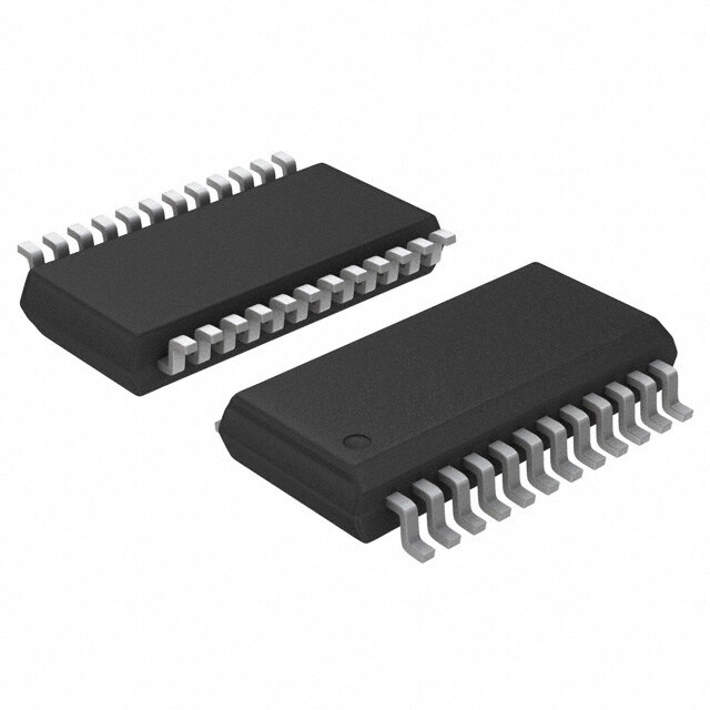
| 描述 | VGA PORT COMPANION 75OHM 24QSOPESD 抑制器 Circuit w/ 75 ohm R 24-Pin |
| 产品分类 | |
| 品牌 | ON Semiconductor |
| 产品手册 | |
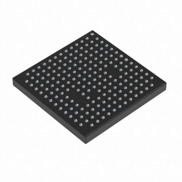
| 产品图片 |
|
| rohs | 符合RoHS无铅 / 符合限制有害物质指令(RoHS)规范要求 |
| 产品系列 | ON Semiconductor PACVGA200QRPActive™ |
| 数据手册 | |
| 产品型号 | PACVGA200QR |
| 产品种类 | ESD 抑制器 |
| 供应商器件封装 | 24-QSOP |
| 其它名称 | PACVGA200QROSCT |
| 包装 | 剪切带 (CT) |
| 商标 | ON Semiconductor |
| 安装类型 | 表面贴装 |
| 封装 | Reel |
| 封装/外壳 | 24-SSOP(0.154",3.90mm 宽) |
| 封装/箱体 | QSOP-24 |
| 工作温度 | 0°C ~ 70°C |
| 工作温度范围 | 0 C to + 70 C |
| 工厂包装数量 | 2500 |
| 应用 | ESD 保护,VGA 端口 |
| 标准包装 | 1 |
| 电压-电源 | 5V |
| 电容 | 4 pF |
| 电流-电源 | 10µA |
| 电流额定值 | 10 uA |
| 端接类型 | SMD/SMT |
| 系列 | PACVGA200 |
| 通道 | 7 Channels |


PDF Datasheet 数据手册内容提取
PACVGA200 VGA Port Companion Circuit Product Description The PACVGA200 incorporates seven channels of ESD protection for all signal lines commonly found in a VGA port. ESD protection is implemented with current steering diodes designed to safely handle the high surge currents encountered with IEC−61000−4−2 Level−4 http://onsemi.com ESD Protection (8kV contact discharge). When a channel is subjected to an electrostatic discharge, the ESD current pulse is diverted via the protection diodes into either the positive supply rail or ground where it may be safely dissipated. Separate positive supply rails are provided for the VIDEO, DDC and SYNC channels to facilitate interfacing with low voltage Video Controller ICs and provide design flexibility in multi−supply−voltage environments. QSOP24 QR SUFFIX Two non−inverting drivers provide buffering for the HSYNC and CASE 492B VSYNC signals from the Video Controller IC (SYNC_IN1, SYNC_IN2). These buffers accept TTL input levels and convert them MARKING DIAGRAM to CMOS output levels that swing between Ground and V 4. CC These drivers have nominal 60(cid:2) output impedance (R ) to match S the characteristic impedance of the HSYNC & VSYNC lines of the PACVGA200QR video cables typically used in PC applications. Two N−channel FETs AWLYWW provide the level shifting function required when the DDC controller is operated at a lower supply voltage than the monitor. Three 75(cid:2) termination resistors suitable for terminating the video signals from the video DAC are also provided. These resistors have separate input PACVGA200QR= Specific Device Code pins to allow insertion of additional EMI filtering, if required, between A = Assembly Location WL = Wafer Lot the termination point and the ESD protection diodes. These resistors Y = Year are matched to better than 2% for excellent signal level matching for WW = Work Week the R/G/B signals. When the PWR_UP input is driven LOW, the SYNC inputs can be ORDERING INFORMATION floated without causing the SYNC buffers to draw any current from the VCC4 supply. When the PWR_UP input is LOW, the SYNC Device Package Shipping† outputs are driven LOW. PACVGA200QR QSOP24 2500/Tape & Reel An internal diode (D1 in schematic on previous page) is also (Pb−Free) provided so that V 3 can be derived from V 4, if desired, by CC CC †For information on tape and reel specifications, connecting V 3 to V_BIAS. In applications where V 4 may be CC CC including part orientation and tape sizes, please powered down, diode D1 blocks any DC current paths from the refer to our Tape and Reel Packaging Specification DDC_OUT pins back to the powered down V 4 rail via the top ESD Brochure, BRD8011/D. CC protection diodes. Features Single Chip Solution for the VGA Port Interface 75(cid:2) Termination Resistors for VIDEO Lines Includes ESD Protection, Level Shifting, and RGB (Matched to 1% Typ.) Termination TTL to CMOS Level−Translating Buffers with Power Seven Channels of ESD Protection for All VGA Port Down Mode for HSYNC and VSYNC Lines Connector Pins Meeting IEC−61000−4−2 Level−4 ESD Bi−Directional Level Shifting N−Channel FETs Requirements (8kV Contact Discharge) Provided for DDC_CLK & DDC_DATA Channels Very Low Loading Capacitance from ESD Protection Compact 24−Pin QSOP Package Diodes on VIDEO Lines, 4pF Typical These Devices are Pb−Free and are RoHS Compliant Applications Notebook Computers with VGA Port Desktop PCs with VGA Port Semiconductor Components Industries, LLC, 2011 1 Publication Order Number: October, 2011 − Rev. 3 PACVGA200/D
PACVGA200 SIMPLIFIED ELECTRICAL SCHEMATIC VCC1 VCC2 VCC3 V_BIAS VCC4 20 SYNC_OUT1 2 12 14 13 D1 1 RS GNDD RC VIDEO_1 34 DDC_IN1 16 15 DDC_OUT1 SYNC_IN1 19 23 SD1 VIDEO_2 5 VIDEO_3 RB GNDD GNDD GNDD 11 6 GNDD PWR_UP GNDD VCC2 GNDD VCC3 RC VCC4 GNDD 22 8 75 GNDD RC GNDD 1 SYNC_OUT2 TERM_1 RS 9 75 DDC_IN2 17 18 DDC_OUT2 TERM_2 21 24 10 75 SYNC_IN2 SD2 TERM_3 GNDD 7 GNDA GNDD GNDD GNDA GNDD PACKAGE / PINOUT DIAGRAMS Top View VCC4 1 24 SD2 VCC1 2 23 SD1 VIDEO_1 3 22 SYNC_OUT2 VIDEO_2 4 21 SYNC_IN2 VIDEO_3 5 20 SYNC_OUT1 GNDD 6 19 SYNC_IN1 GNDA 7 18 DDC_OUT2 TERM_1 8 17 DDC_IN2 TERM_2 9 16 DDC_IN1 TERM_3 10 15 DDC_OUT1 PWR_UP 11 14 VCC3 VCC2 12 13 V_BIAS 24−Pin QSOP http://onsemi.com 2
PACVGA200 Table 1. PIN DESCRIPTIONS Lead(s) Name Description 1 VCC4 Positive voltage supply pin. This is an isolated VCC pin for the SYNC_1, SYNC_2, SD1 andSD2 circuits. 2 VCC1 Positive voltage supply pin. This is an isolated VCC pin for the VIDEO_1, VIDEO_2 andVIDEO_3 ESD circuits. 3−5 VIDEO_1, VIDEO_2, VIDEO_3 RGB Video Protection Channels. These pins tie to the RGB video lines (for example, theBlue signal) between the VGA controller device and the video connector. 6 GNDD Digital Ground reference supply pin. 7 GNDA Ground reference supply pin for TERM_1, TERM_2 and TERM_3 pins. 8−10 TERM_1, TERM_2, TERM_3 RGB Video Termination Channels. These pins tie to the RGB video lines (for example, theBlue signal) providing a 75(cid:2) termination to GNDA for the given video channel. 11 PWR_UP Sync Signal Output 1. Ties to the video connector side of one of the sync lines (forexample the Horizontal Sync signal). 12 VCC2 Positive voltage supply pin. This is an isolated VCC pin for the DDC_IN1 and DDC_IN2 input circuits. Defines the logic one level for the DDC_OUTn outputs. 13 V_BIAS Used to derive VCC3 from VCC4 input. 14 VCC3 Positive voltage supply pin. This is an isolated VCC pin for the DDC_OUT1 andDDC_OUT2 ESD protection circuits. 15 DDC_OUT1 DDC Signal Output 1. Connects to the connector side of one of the DDC signals (forexample, the bidirectional DDC_Data serial line). 16 DDC_IN1 DDC Signal Input 1. Connects to the VGA Controller side of one of the DDC signals (forexample, the bidirectional DDC_Data serial line). 17 DDC_IN2 DDC Signal Input 2. Connects to the VGA Controller side of one of the DDC signals (forexample, the bidirectional DDC_Clk). 18 DDC_OUT2 DDC Signal Output 2. Connects to the connector side of one of the DDC signals (forexample, the bidirectional DDC_Clk). 19 SYNC_IN1 Sync Signal Buffer Input 1. Connects to the VGA Controller side of one of the sync lines (for example, the Horizontal Sync signal). 20 SYNC_OUT1 Sync Signal Buffer Output 1. Connects to the video connector side of one of the sync lines (for example the Horizontal Sync signal). 21 SYNC_IN2 Sync Signal Buffer Input 2. Connects to the VGA Controller side of one of the sync lines (for example, the Vertical Sync signal). 22 SYNC_OUT2 Sync Signal Buffer Output 2. Connects to the video connector side of one of the sync lines (for example the Vertical Sync signal). 23 SD1 Sync Signal Filter 1. Connects to the video connector side of one of the sync lines (forexample the Vertical Sync signal). 24 SD2 Sync Signal Filter 2. Connects to the video connector side of one of the sync lines (forexample the Horizontal Sync signal). http://onsemi.com 3
PACVGA200 SPECIFICATIONS Table 2. ABSOLUTE MAXIMUM RATINGS Parameter Rating Units VCC1, VCC2, VCC3 and VCC4 Supply Voltage [GND − 0.5] to +6.0 V Diode D1 Forward DC Current 100 (cid:3)A Storage Temperature Range −65 to +150 C DC Voltage at Inputs V VIDEO_1, VIDEO_2, VIDEO_3 [GND − 0.5] to [VCC1 + 0.5] TERM_1, TERM_2, TERM_3 −6.0, +6.0 DDC_IN1, DDC_IN2 [GND − 0.5] to [VCC2 + 0.5] DDC_OUT1, DDC_OUT2 [GND − 0.5] to [VCC3 + 0.5] SYNC_IN1, SYNC_IN2 [GND − 0.5] to [VCC4 + 0.5] Package Power Rating 1000 mW Stresses exceeding Maximum Ratings may damage the device. Maximum Ratings are stress ratings only. Functional operation above the Recommended Operating Conditions is not implied. Extended exposure to stresses above the Recommended Operating Conditions may affect device reliability. Table 3. STANDARD OPERATING CONDITIONS Parameter Rating Units Operating Temperature Range 0 to +70 C Table 4. ELECTRICAL OPERATING CHARACTERISTICS (Note 1) Symbol Parameter Conditions Min Typ Max Units ICC1 VCC1 Supply Current VCC1 = 5.0V, VIDEO inputs at VCC1 10 (cid:3)A or GND level ICC2, VCC2 & VCC3 Supply Current VCC2 = VCC3 = 5.0V 10 (cid:3)A ICC3 ICC4 VCC4 Supply Current VCC4 = 5.0V, SYNC Inputs at GND or 10 (cid:3)A VCC4 Level, PWR−UP pin at VCC4, SYNC Outputs Unloaded VCC4 = 5.0V, SYNC Inputs at 3.0V, 200 (cid:3)A PWR−UP Pin at VCC4, SYNC Outputs Unloaded VCC4 = 5.0V, PWR−UP Input at GND, 10 (cid:3)A SYNC Outputs Unloaded VBIAS VBIAS Open Circuit Voltage No External Current Drawn from VCC4−0.8 V VBIAS Pin RT Video Termination Resistance 71.25 75 78.75 (cid:2) RT Resistance Matching 1 2 % VIH Logic High Input Voltage VCC4 = 5.0V (Note 2) 2.0 V VIL Logic Low Input Voltage VCC4 = 5.0V (Note 2) 0.8 V VOH Logic High Output Voltage IOH = −4mA, VCC4 = 5.0V (Note 2) 4.5 4.8 V VOL Logic Low Output Voltage IOL = 4mA, VCC4 = 5.0V (Note 2) 0.18 0.32 V ROH Output Resistance (Note 2) 50 125 (cid:2) ROL 45 80 (cid:2) RB, RP Resistor Value PWR_UP = VCC3 = 5.0V 0.5 1.0 2.0 M(cid:2) RC VCC2 Pull−down Resistor Value VCC2 = 3.0V 0.5 1.5 3.0 M(cid:2) IN Input Current (cid:3)A VIDEO Inputs VCC1= 5.0V, VIN = VCC1 or GND 1 HSYNC, VSYNC Inputs VCC4 = 5.0V, VIN = VCC4 or GND 1 http://onsemi.com 4
PACVGA200 Table 4. ELECTRICAL OPERATING CHARACTERISTICS (Note 1) Symbol Parameter Conditions Min Typ Max Units IOFF Off−State Leakage Current, (VCC2 − VDDC_IN) 0.4V, 10 (cid:3)A VDDC_OUT = VCC2 Level−Shifting NFET (VCC2 − VDDC_OUT) 0.4V, 10 VDDC_IN = VCC2 VON Voltage Drop Across Level VCC2 = 2.5V, VS = GND, IDS = 3mA 0.15 V Shifting NFET when Turned ON CIN Input Capacitance pF VIDEO_1,VIDEO_2 & VIDEO_3 VCC1 = 5.0V, VIN = 2.5V, 3.0 4.0 5.0 Inputs Measured at 1MHz VCC1 = 2.5V, VIN = 1.25V, 3.0 4.5 5.6 Measured at 1MHz tPLH SYNC Drivers L H Propagation CL = 50pF, VCC = 5.0V, 8.0 12.0 ns Delay Input tR and tF 5ns tPHL SYNC Drivers H L Propagation CL = 50pF, VCC = 5.0V, 8.0 12.0 ns Delay Input tR and tF 5ns tR, tF SYNC Drivers Output Rise & Fall CL = 50pF, VCC = 5.0V, 5.0 7.0 10.0 ns Times Input tR and tF 5ns (Measured 10% − 90%) VESD ESD Withstand Voltage VCC1 = VCC3 = VCC4 = 5V (Note 3) 8 kV 1. All parameters specified over standard operating conditions unless otherwise noted. 2. This parameter applies only to the HSYNC and VSYNC channels. HSYNC and VSYNC have 8mA drivers with RS added in series to terminate transmission line. 3. Per the IEC−61000−4−2 International ESD Standard, Level 4 contact discharge method. VCC1, VCC3 and VCC4 must be bypassed to GND via a low impedance ground plane with a 0.2(cid:3)F, low inductance, chip ceramic capacitor at each supply pin. ESD pulse is applied between the applicable pins and GND. ESD pulse can be positive or negative with respect to GND. Applicable pins are: VIDEO_1, VIDEO_2, VIDEO_3, SYNC_OUT1, SD1, SYNC_OUT2, SD2, DDC_OUT1 and DDC_OUT2. All other pins are ESD protected to the industry standard 2kV per the Human Body Model (MIL−STD−883, Method 3015). http://onsemi.com 5
PACVGA200 TEST CIRCUIT INFORMATION Average Current through V 4 (I 4) CC CC The circuit in Figure 1 was used to characterize I 4 current as SYNC_IN signal frequency varies. A square wave signal CC was connected to the input of one of the SYNC buffers (i.e. pin 19 or pin 21). The frequency of this signal was varied between 0and100kHz. The risetime and falltime was kept constant at 10ns. Three different values of C1 were used: 0pF, 50pF and 100pF. The results are plotted in Figure 2. VCC4 +5 V ICC4 SYNC_IN SYNC_OUT 3.3 V 0 V C1 Figure 1. Sync Buffer I 4 Test Circuit CC A) (cid:3) 4 ( C C I Frequency (kHz) Figure 2. I 4 vs. SYNC_IN Frequency Performance Data CC http://onsemi.com 6
PACVGA200 APPLICATION INFORMATION DDC_VCC VIDEO_DAC VCC 5 V 0.2 (cid:3)F 0.2 (cid:3)F 0.2 (cid:3)F 0.2 (cid:3)F R1 R2 GNDD 12 2 14 13 r o GNDD VCC2 VCC1 VCC3 V_BIAS ect n 16 n DDC_Data DDC_IN1 1 Co DDC_Clk 17 DDC_IN2 VCC4 11 eo PWR_UP d 19 Vi er H−Sync SYNC_IN1 roll V−Sync 21 SYNC_IN2 nt o 15 C DDC_OUT1 DDC_Data o 8 18 e Red TERM_1 DDC_OUT2 DDC_Clk Vid Green 9 TERM_2 10 20 Blue ÎÎÎÎÎÎ TERM_3 SYNC_OUT1 22 SYNC_OUT2 ÎÎÎÎÎÎ ÎÎÎ V V V F F F Î**ÎÎ**ÎÎ**Î ÎS ÎSÎ PACVGA200 F F * * Î* Î*Î 3 VIDEO_1 4 23 VIDEO_2 SD1 H−Sync 5 24 VIDEO_3 SD2 V−Sync GNDA GNDD 7 6 R G B VF** − VIDEO EMI Filter SF** − SYNC EMI Filter Figure 3. Typical Connection Diagram A resistor may be necessary between the V 3 pin and ground if protection against a stream of ESD pulses is required while CC the PACVGA200 is in the power−down state. The value of this resistor should be chosen such that the extra charge deposited into the V 3 bypass capacitor by each ESD pulse will be discharged before the next ESD pulse occurs. The maximum ESD CC repetition rate specified by the IEC−61000−4−2 standard is one pulse per second. When the PACVGA200 is in the power−up state, an internal discharge resistor is connected to ground via an FET switch for this purpose. For the same reason, V 1 and V 4 may also require bypass capacitor discharging resistors to ground if there are no other CC CC components in the system to provide a discharge path to ground. GNDA, the reference voltage for the 75(cid:2) resistors is not connected internally to GNDD and should ideally be connected to the ground of the video DAC IC. http://onsemi.com 7
PACVGA200 PACKAGE DIMENSIONS QSOP24 NB CASE 492B−01 ISSUE A 2X NOTES: 0.20 C D 1. DIMENSIONING AND TOLERANCING PER ASME D Y14.5M, 1994. D 2. CONTROLLING DIMENSION: MILLIMETERS. 24 A 13 C GPLAAUNGEE 3. DPRIMOETNRSUIOSINO Nb .DOES NOT INCLUDE DAMBAR L2 4. DIMENSION D DOES NOT INCLUDE MOLD FLASH, PROTRUSIONS, OR GATE BURRS. MOLD FLASH, PROTRUSIONS, OR GATE BURRS SHALL NOT EXCEED 0.15 PER SIDE. DIMENSION E1 DOES NOT INCLUDE INTERLEAD FLASH OR PROTRUSION. E1 E L C INTERLEAD FLASH OR PROTRUSION SHALL NOT EXCEED 0.15 PER SIDE. D AND E1 ARE DETAIL A DETERMINED AT DATUM H. 2X 5. DATUMS A AND B ARE DETERMINED AT DATUM H. 0.20 C D 2X 12 TIPS MILLIMETERS 1 12 0.25 C D DIM MIN MAX 24Xb A 1.35 1.75 e A1 0.10 0.25 B 0.25 M C A-B D h x 45(cid:2) b 0.20 0.30 C 0.19 0.25 0.10 C A H D 8.65 BSC E 6.00 BSC E1 3.90 BSC e 0.635 BSC h 0.22 0.50 0.10 C L 0.40 1.27 24X A1 C SPELAATNIENG DETAIL A M LM2 00 .(cid:2) 25 BSC8 (cid:2) SOLDERING FOOTPRINT GENERIC 24X 24X MARKING DIAGRAM* 0.42 1.12 24 13 6.40 *This information is generic. Please refer 1 12 to device data sheet for actual part 0.635 marking. Pb−Free indicator, “G”, may PITCH DIMENSIONS: MILLIMETERS or not be present. ON Semiconductor and are registered trademarks of Semiconductor Components Industries, LLC (SCILLC). SCILLC reserves the right to make changes without further notice to any products herein. SCILLC makes no warranty, representation or guarantee regarding the suitability of its products for any particular purpose, nor does SCILLC assume any liability arising out of the application or use of any product or circuit, and specifically disclaims any and all liability, including without limitation special, consequential or incidental damages. “Typical” parameters which may be provided in SCILLC data sheets and/or specifications can and do vary in different applications and actual performance may vary over time. All operating parameters, including “Typicals” must be validated for each customer application by customer’s technical experts. SCILLC does not convey any license under its patent rights nor the rights of others. SCILLC products are not designed, intended, or authorized for use as components in systems intended for surgical implant into the body, or other applications intended to support or sustain life, or for any other application in which the failure of the SCILLC product could create a situation where personal injury or death may occur. Should Buyer purchase or use SCILLC products for any such unintended or unauthorized application, Buyer shall indemnify and hold SCILLC and its officers, employees, subsidiaries, affiliates, and distributors harmless against all claims, costs, damages, and expenses, and reasonable attorney fees arising out of, directly or indirectly, any claim of personal injury or death associated with such unintended or unauthorized use, even if such claim alleges that SCILLC was negligent regarding the design or manufacture of the part. SCILLC is an Equal Opportunity/Affirmative Action Employer. This literature is subject to all applicable copyright laws and is not for resale in any manner. PUBLICATION ORDERING INFORMATION LITERATURE FULFILLMENT: N. American Technical Support: 800−282−9855 Toll Free ON Semiconductor Website: www.onsemi.com Literature Distribution Center for ON Semiconductor USA/Canada P.O. Box 5163, Denver, Colorado 80217 USA Europe, Middle East and Africa Technical Support: Order Literature: http://www.onsemi.com/orderlit Phone: 303−675−2175 or 800−344−3860 Toll Free USA/Canada Phone: 421 33 790 2910 Fax: 303−675−2176 or 800−344−3867 Toll Free USA/Canada Japan Customer Focus Center For additional information, please contact your local Email: orderlit@onsemi.com Phone: 81−3−5817−1050 Sales Representative http://onsemi.com PACVGA200/D 8