ICGOO在线商城 > 集成电路(IC) > 线性 - 放大器 - 仪表,运算放大器,缓冲器放大器 > PA95
 Datasheet下载
- 型号: PA95
- 制造商: Apex Microtechnology Corporation
- 库位|库存: xxxx|xxxx
- 要求:
| 数量阶梯 | 香港交货 | 国内含税 |
| +xxxx | $xxxx | ¥xxxx |
查看当月历史价格
查看今年历史价格
PA95产品简介:
ICGOO电子元器件商城为您提供PA95由Apex Microtechnology Corporation设计生产,在icgoo商城现货销售,并且可以通过原厂、代理商等渠道进行代购。 PA95价格参考。Apex Microtechnology CorporationPA95封装/规格:线性 - 放大器 - 仪表,运算放大器,缓冲器放大器, 功率 放大器 1 电路 8-SIP。您可以下载PA95参考资料、Datasheet数据手册功能说明书,资料中有PA95 详细功能的应用电路图电压和使用方法及教程。
Apex Microtechnology的PA95是一款高性能线性放大器,属于仪表、运算及缓冲放大器类别。其应用场景广泛,特别是在需要高精度、高功率和低失真的场合。以下是PA95的主要应用场景:

1. 工业自动化与控制:
   PA95可用于工业自动化中的精密传感器信号放大,例如压力传感器、温度传感器或位移传感器等。其高增益带宽积和低噪声特性使其适合处理微弱信号,同时提供足够的输出功率以驱动后续负载。

2. 医疗设备:
   在医疗领域,如超声波设备、心电图(ECG)或脑电图(EEG)系统中,PA95可以作为信号调理放大器,将生物电信号放大到可检测水平,同时保持信号的完整性。

3. 测试与测量仪器:
   该型号适用于高性能示波器、信号发生器或其他测试设备中,用于精确地放大输入信号或将信号传输到负载。其稳定的性能和宽动态范围有助于提高测量精度。

4. 音频处理:
   在专业音频应用中,PA95可以用作前置放大器或功率放大器的一部分,提供高质量的音频信号放大,满足高保真需求。

5. 航空航天与国防:
   PA95具有良好的抗电磁干扰能力和稳定性,因此在航空航天和国防领域的关键任务系统中也有应用,例如雷达信号处理、导航系统或通信设备。

6. 电源管理与驱动:
   它还可以用作小型电机驱动器或LED驱动器中的功率级放大器,提供精确的电流控制。

总之,PA95凭借其出色的电气特性和可靠性,成为许多高要求应用的理想选择。具体使用时需根据实际电路设计需求进行匹配和优化。
| 参数 | 数值 |
| -3db带宽 | - |
| 产品目录 | 集成电路 (IC) |
| 描述 | IC OPAMP POWER 10MHZ 8SIP |
| 产品分类 | Linear - Amplifiers - Instrumentation, OP Amps, Buffer Amps |
| 品牌 | Apex Microtechnology |
| 数据手册 | |
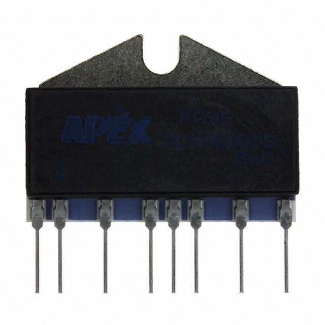
| 产品图片 |
|
| 产品型号 | PA95 |
| rohs | 无铅 / 符合限制有害物质指令(RoHS)规范要求 |
| 产品系列 | Apex Precision Power® |
| 产品培训模块 | http://www.digikey.cn/PTM/IndividualPTM.page?site=cn&lang=zhs&ptm=30464 |
| 产品目录页面 | |
| 供应商器件封装 | 8-SIP |
| 其它名称 | 598-1335 |
| 包装 | 管件 |
| 压摆率 | 30 V/µs |
| 增益带宽积 | 10MHz |
| 安装类型 | 通孔 |
| 封装/外壳 | 12-SIP(8 引线) |
| 工作温度 | -25°C ~ 85°C |
| 应用说明 | |
| 放大器类型 | 功率 |
| 标准包装 | 1 |
| 特色产品 | http://www.digikey.cn/product-highlights/zh/pa95-mosfet-operational-amplifier/50294 |
| 电压-电源,单/双 (±) | 100 V ~ 900 V, ±50 V ~ 450 V |
| 电压-输入失调 | 500µV |
| 电流-电源 | 1.6mA |
| 电流-输入偏置 | 200pA |
| 电流-输出/通道 | 100mA |
| 电路数 | 1 |
| 输出类型 | - |
| 配用 | /product-detail/zh/EK19/598-1462-ND/1762065 |


PDF Datasheet 数据手册内容提取
PA95 RoHS High Voltage Power Operational Amplifiers COMPLIANT FEATURES • High Voltage— 900V (±450V) • Low Quiescent Current — 1.6mA • Output Current — 100mA • Programmable Current Limit APPLICATIONS • High Voltage Instrumentation • Programmable Power Supplies Up To ±430V • Mass Spectrometers • Semiconductor Measurement Equipment DESCRIPTION The PA95 is a high voltage, MOSFET operational amplifier designed as a low cost solution for driving con‐ tinuous output currents up to 100mA and pulse currents up to 200mA into capacitive loads. The safe operat‐ ing area (SOA) has no second breakdown limitations and can be observed for all load types by choosing an appropriate current limiting resistor. The MOSFET output stage is biased AB for linear operation. External compensation provides flexibility in choosing bandwidth and slew rate for the application. Apex Microtech‐ nology’s Power SIP uses minimum board space allowing for high density circuit boards. The Power SIP is elec‐ trically isolated. Isolating thermal washers (TW13) are recommended to prevent arcing from pins to heatsink. Figure 1: Equivalent Schematic 12 +VS R1A R1B C2 R3 Q3 Q1 Q2 R4 Q4 Q6 6 ILIM 4 CC2 8 Q5 CC1 Q8 R7 Q5A Q5B Q11 1 7 –IN R9 R10 OUT Q21 R11 R12 Q29 2 Q14 R19 +IN Q30 Q29 R20 R27 –VS 10 © Apex Microtechnology Inc. Sep 2017 www.apexanalog.com All rights reserved PA95U Rev Q
PA95 TYPICAL CONNECTION Figure 2: Typical Connection R F 100 k +V S C C 10 9 10μF 100nF C C 10pF R IN +V S V OUT + 1 k CC PA95 CC CL -V S R L R CL -V S C C 8 7 10μF 100nF 2 PA95U Rev Q
PA95 PINOUT AND DESCRIPTION TABLE Figure 3: External Connections Pin Number Name Description 1 ‐IN The inverting input. 2 +IN The non‐inverting input. Compensation capacitor connection. Select value based on Phase Compensation. 4, 6 CC See applicable section. 7 OUT The output. Connect this pin to load and to the feedback resistors. Connect to the current limit resistor. Output current flows into/out of this pin 8 CL through R . The output pin and the load are connected to the other side of R . CL CL 10 ‐Vs The negative supply rail. 12 +Vs The positive supply rail. PA95U Rev Q 3
PA95 SPECIFICATIONS Unless otherwise noted: T = 25°C, DC input specifications are ± value given. Power supply voltage is typ‐ C ical rating. C = 4.7pF. c ABSOLUTE MAXIMUM RATINGS Parameter Symbol Min Max Units Supply Voltage, +V to ‐V +V to ‐V 900 V S S s s Output Current, source, sink, within SOA I 200 mA O Power Dissipation, continuous @ T = 25°C P 30 W C D Input Voltage, differential V ‐20 20 V IN (Diff) Input Voltage, common mode 1 Vcm ‐VS +VS V Temperature, pin solder, 10s max. 260 °C Temperature, junction 2 TJ 150 °C Temperature Range, storage ‐55 125 °C Operating Temperature Range, case T ‐40 85 °C C 1. Although supply voltages can range up to ± 450V the input pins cannot swing over this range. The input pins must be at least 30V from either supply rail but not more than 500V from either supply rail. See text for a more complete descrip‐ tion of the common mode voltage range. 2. Long term operation at the maximum junction temperature will result in reduced product life. Derate internal power dis‐ sipation to achieve high MTTF. The PA95 is constructed from MOSFET transistors. ESD handling procedures must be observed. CAUTION The exposed substrate contains beryllia (BeO). Do not crush, machine, or subject to tempera‐ tures in excess of 850°C to avoid generating toxic fumes. 4 PA95U Rev Q
PA95 INPUT Parameter Test Conditions Min Typ Max Units Offset Voltage, initial 0.5 5 mV Offset Voltage vs. temperature Full temp range 15 50 µV/°C Offset Voltage vs. supply 10 25 µV/V Offset Voltage vs. time 75 µV/khr Bias Current, initial 200 2000 pA Bias Current vs. supply 4 pA/V Offset Current, initial 50 500 pA Input Resistance, DC 1011 Ω Input Capacitance 4 pF Common Mode Voltage Range 1 VS=±250V ±VS ∓ 30 V Common Mode Rejection, DC V = ±90V 80 98 dB CM Noise 10 kHz bandwidth, R = 1 kΩ 2 µV RMS S 1. Although supply voltages can range up to ± 450V the input pins cannot swing over this range. The input pins must be at least 30V from either supply rail but not more than 500V from either supply rail. See text for a more complete descrip‐ tion of the common mode voltage range. GAIN Parameter Test Conditions Min Typ Max Units Open Loop @ 15 Hz R = 5 kΩ 94 118 dB L Gain Bandwidth Product @ 1 MHz R = 5 kΩ 10 MHz L Power Bandwidth R = 5 kΩ 20 kHz L Phase Margin, A = 10 Full temp range 60 ° V OUTPUT Parameter Test Conditions Min Typ Max Units Voltage Swing IO = 70mA ±VS ∓ 24 ±VS ∓ 20 V Current, Continuous 100 mA Slew Rate, A = 100 C =4.7pF 30 V/µs V C Settling Time, to 0.1% 2V Step 1 µs Resistance no load 100 Ω PA95U Rev Q 5
PA95 POWER SUPPLY Parameter Test Conditions Min Typ Max Units Voltage 1 ±50 ±300 ±450 V Current, quiescent 1.6 2.2 mA 1. Derate max supply rating 0.625 V/°C below 25°C case. No derating needed above 25°C case. THERMAL Parameter Test Conditions Min Typ Max Units Resistance, AC, junction to case 1 Full temp range, F > 60 Hz 2.5 °C/W Resistance, DC, junction to case Full temp range, F < 60 Hz 4.2 °C/W Resistance, junction to air Full temp range 30 °C/W Temperature Range, case ‐25 +85 °C 1. Rating applies if the output current alternates between both output transistors at a rate faster than 60 Hz. 6 PA95U Rev Q
PA95 TYPICAL PERFORMANCE GRAPHS Figure 4: Power Derating Figure 5: Quiescent Current 30 1.08 ) (cid:116) 25 (cid:87)(cid:3)(cid:894) T = T ) 1.04 (cid:374)(cid:853)(cid:3) C (X (cid:415)(cid:381) 20 t, I (cid:258) n 1.00 (cid:393) e (cid:24)(cid:349)(cid:400)(cid:400)(cid:349) 15 Curr (cid:286)(cid:396)(cid:3) nt 0.96 (cid:449) e c (cid:381) 10 s (cid:87) e (cid:374)(cid:258)(cid:367)(cid:3) T = T Qui 0.92 (cid:286)(cid:396) 5 A (cid:410) (cid:374) (cid:47) 0 0.88 0 25 50 75 100 125 150 0 200 400 600 800 1000 Temperature, T (°C) Total Supply Voltage, V (V) S Figure 6: Small Signal Response Figure 7: Phase Response 120 -90 100 -135 ) B d ain, A ( 80 CC = 4.7pF (cid:711)(cid:3)(cid:894)(cid:931)(cid:895) -180 CC = 4.7pF p G 60 se, -225 o a o h n L 40 P -270 e p O 20 -315 0 -360 10 100 1k 10k 100k 1M 10M 1M 2M 3M 4M 5M Frequency, F (Hz) Frequency, F (Hz) PA95U Rev Q 7
PA95 Figure 8: Output Voltage Swing Figure 9: Power Response 40 1k ) V ( O 500 V V- S 32 25°C ) P-P ply, T =C 1 = 85°C V(VO om Sup 24 T TC = 2 5° C oltage, 200 CC = 4.7pF op Fr 16 T C = –55°C put V r C t D u 100 e 8 O g a t ol V 4 50 0 20 40 60 80 100 10k 100k 300k Output Current, I (mA) Frequency, F (Hz) o Figure 10: Current Limit Figure 11: Input Noise 200 20 (cid:460)(cid:895) 15 120 (cid:44) (cid:1103) (cid:895) 100 (cid:115)(cid:876) (cid:4) (cid:374) t, I(mLIM 5700 age, V(cid:3)(cid:894)N 170 mi olt Li V nt 30 e 5 re ois r N u C 20 t u p 3 n I 10 2 3 5 10 20 50 100150 10 100 1k 10k 1M Current Limit Resistor, R (cid:3)(cid:894)(cid:591)(cid:895) Frequency, F (Hz) CL 8 PA95U Rev Q
PA95 SAFE OPERATING AREA (SOA) Figure 12: Safe Operating Area 250 A) 150 100 m m S ( 100 2 S 0 V 0 (cid:3)(cid:882) (cid:24) mS (cid:396)(cid:3) (cid:18)(cid:853)(cid:3) (cid:381) (cid:100) V(cid:1085)S 50 (cid:24)(cid:18)(cid:853)(cid:3) C= 25°C (cid:410)(cid:3)(cid:3) (cid:100)C = (cid:374) 8 (cid:396)(cid:286) 25 (cid:24)(cid:18)(cid:853)(cid:3)(cid:100) 5°C (cid:396) (cid:437) C= 1 (cid:18) 2 (cid:3) 15 5° (cid:410) C (cid:437) (cid:393) (cid:410) 10 (cid:437) (cid:75) (cid:87)(cid:437)(cid:367)(cid:400)(cid:286)(cid:3)(cid:18)(cid:437)(cid:396)(cid:448)(cid:286)(cid:400)(cid:3)(cid:923) (cid:1005)(cid:1004)(cid:1081)(cid:3)(cid:24)(cid:437)(cid:410)(cid:455)(cid:3)(cid:18)(cid:455)(cid:272)(cid:367)(cid:286)(cid:3)(cid:68)(cid:258)(cid:454) 5 50 100 200 500 1k (cid:94)(cid:437)(cid:393)(cid:393)(cid:367)(cid:455)(cid:3)(cid:410)(cid:381)(cid:3)(cid:75)(cid:437)(cid:410)(cid:393)(cid:437)(cid:410)(cid:3)(cid:24)(cid:349)(cid:299)(cid:286)(cid:396)(cid:286)(cid:374)(cid:415)(cid:258)(cid:367)(cid:853)(cid:3)V - V (V) S O PA95U Rev Q 9
PA95 GENERAL Please read Application Note 1 “General Operating Considerations” which covers stability, supplies, heat sinking, mounting, current limit, SOA interpretation, and specification interpretation. Visit www.apexana‐ log.com for Apex Microtechnology’s complete Application Notes library, Technical Seminar Workbook, and Evaluation Kits. TYPICAL APPLICATION Piezo positioning may be applied to the focusing of segmented mirror systems. The composite mirror may be composed of hundreds of elements, each requiring focusing under computer control. In such com‐ plex systems the PA95 reduces the costs of power supplies and cooling with its advantages of low cost and low quiescent power consumption while increasing circuit density with the SIP. Figure 13: Typical Application PHASE COMPENSATION Gain C C ≥100 4.7pF Note:C rated for full supply voltage C CURRENT LIMIT For proper operation, the current limit resistor (R ) must be connected as shown in the external connec‐ CL tion diagram. The minimum value is 3.5 ohm, however for optimum reliability the resistor value should be set as high as possible. The value is calculated as follows; with the maximum practical value of 150 ohms. 0.7V R = ------------------- CL I A LIM COMMON MODE INPUT RANGE Operational amplifiers are usually designed to have a common mode input voltage range that approxi‐ mates the power supply voltage range. However, to keep the cost as low as possible and still meet the requirements of most applications the common mode input voltage range of the PA95 is restricted. The input 10 PA95U Rev Q
PA95 pins must always be a least 30V from either supply voltage but never more than 500V. This means that the PA95 cannot be used in applications where the supply voltages are extremely unbalanced. For example, sup‐ ply voltages of +800V and –100V would not be allowed in an application where the non‐inverting pin is grounded because in normal operation both input pins would be at 0V and the difference voltage between the positive supply and the input pins would be 800V. In this kind of application, however, supply voltages +500V and ‐100V does meet the input common mode voltage range requirements since the maximum differ‐ ence voltage between the inputs pins and the supply voltage is 500V (the maximum allowed). The output has no such restrictions on its voltage swing. The output can swing within 24V of either supply voltage regardless of value so long as the total supply voltage does not exceed 900V. INPUT PROTECTION Although the PA95 can withstand differential input voltages up to ±20V, additional external protection is recommended. In most applications 1N4148 or 1N914 signal diodes are sufficient (D1, D2 in Figure 14A). In more demanding applications where low leakage or low capacitance are of concern 2N4416 or 2N5457‐ 2N5459 JFETs connected as diodes will be required (Q1, Q2 in Figure 14B). In either case the input differential voltage will be clamped to ±0.7V. This is sufficient overdrive to produce maximum power bandwidth. Note that this protection does not automatically protect the amplifier from excessive common mode input volt‐ ages. Figure 14: Overvoltage Protection PA95U Rev Q 11
PA95 POWER SUPPLY PROTECTION Unidirectional zener diode transient suppressors are recommended as protection on the supply pins. The zeners clamp transients to voltages within the power supply rating and also clamp power supply reversals to ground. Whether the zeners are used or not, the system power supply should be evaluated for transient per‐ formance including power‐on overshoot and power‐off polarity reversal as well as line regulation. Conditions which can cause open circuits or polarity reversals on either power supply rail should be avoided or protected against. Reversals or opens on the negative supply rail is known to induce input stage failure. Unidirectional transzorbs prevent this, and it is desirable that they be both electrically and physically as close to the amplifier as possible. STABILITY The PA95 is stable at gains of 10 or more with a NPO (COG) compensation capacitor of 4.7pF. The com‐ pensation capacitor, Cc, in the external connections diagram must be rated at 1000V working voltage and mounted closely to pins 4 and 6 to prevent spurious oscillation. A compensation capacitor less than 4.7pF is not recommended. EXTERNAL COMPONENTS Of great importance are the voltage rating and voltage coefficient of the gain setting feedback resistor. Typical voltage ratings of low wattage resistors are 150 to 250V. Up to 500 V can appear across the feedback resistor. High voltage rated resistors can be obtained. However a 1 MΩ feedback resistor composed of five 200k resistors in series will produce the proper voltage rating. CAUTIONS The operating voltages of the PA95 are potentially lethal. During circuit design develop a functioning cir‐ cuit at the lowest possible voltages. Clip test leads should be used for “hands off” measurements while trou‐ bleshooting. 12 PA95U Rev Q
PA95 PACKAGE OPTIONS Part Number Apex Package Style Description PA95 DQ 8‐Pin SIP PA95EC EC 8‐Pin SIP w/ formed leads PACKAGE STYLE DQ PA95U Rev Q 13
PA95 PACKAGE STYLE EC NEED TECHNICAL HELP? CONTACT APEX SUPPORT! For all Apex Microtechnology product questions and inquiries, call toll free 800-546-2739 in North America. For inquiries via email, please contact apex.support@apexanalog.com. International customers can also request support by contacting their local Apex Microtechnology Sales Representative. To find the one nearest to you, go to www.apexanalog.com IMPORTANT NOTICE Apex Microtechnology, Inc. has made every effort to insure the accuracy of the content contained in this document. However, the information is subject to change without notice and is provided "AS IS" without warranty of any kind (expressed or implied). Apex Microtechnology reserves the right to make changes without further notice to any specifications or products mentioned herein to improve reliability. This document is the property of Apex Microtechnology and by furnishing this information, Apex Microtechnology grants no license, expressed or implied under any patents, mask work rights, copyrights, trademarks, trade secrets or other intellectual property rights. Apex Microtechnology owns the copyrights associated with the information contained herein and gives consent for copies to be made of the information only for use within your organization with respect to Apex Microtechnology integrated circuits or other products of Apex Microtechnology. This consent does not extend to other copying such as copying for general distribution, advertising or promotional purposes, or for creating any work for resale. APEX MICROTECHNOLOGY PRODUCTS ARE NOT DESIGNED, AUTHORIZED OR WARRANTED TO BE SUITABLE FOR USE IN PRODUCTS USED FOR LIFE SUPPORT, AUTOMOTIVE SAFETY, SECURITY DEVICES, OR OTHER CRITICAL APPLICATIONS. PRODUCTS IN SUCH APPLICATIONS ARE UNDERSTOOD TO BE FULLY AT THE CUSTOMER OR THE CUSTOMER’S RISK. Apex Microtechnology, Apex and Apex Precision Power are trademarks of Apex Microtechnology, Inc. All other corporate names noted herein may be trademarks of their respective holders. 14 PA95U Rev Q