ICGOO在线商城 > 集成电路(IC) > 线性 - 放大器 - 仪表,运算放大器,缓冲器放大器 > PA78DK
 Datasheet下载
- 型号: PA78DK
- 制造商: Apex Microtechnology Corporation
- 库位|库存: xxxx|xxxx
- 要求:
| 数量阶梯 | 香港交货 | 国内含税 |
| +xxxx | $xxxx | ¥xxxx |
查看当月历史价格
查看今年历史价格
PA78DK产品简介:
ICGOO电子元器件商城为您提供PA78DK由Apex Microtechnology Corporation设计生产,在icgoo商城现货销售,并且可以通过原厂、代理商等渠道进行代购。 PA78DK价格参考¥询价-¥询价。Apex Microtechnology CorporationPA78DK封装/规格:线性 - 放大器 - 仪表,运算放大器,缓冲器放大器, 功率 放大器 1 电路 20-PSOP。您可以下载PA78DK参考资料、Datasheet数据手册功能说明书,资料中有PA78DK 详细功能的应用电路图电压和使用方法及教程。
| 参数 | 数值 |
| -3db带宽 | - |
| 产品目录 | 集成电路 (IC) |
| 描述 | IC OPAMP POWER 1MHZ 20PSOP |
| 产品分类 | Linear - Amplifiers - Instrumentation, OP Amps, Buffer Amps |
| 品牌 | Apex Microtechnology |
| 数据手册 | |
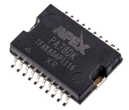
| 产品图片 |
|
| 产品型号 | PA78DK |
| rohs | 无铅 / 符合限制有害物质指令(RoHS)规范要求 |
| 产品系列 | Apex Precision Power® |
| 产品培训模块 | http://www.digikey.cn/PTM/IndividualPTM.page?site=cn&lang=zhs&ptm=30464 |
| 产品目录页面 | |
| 供应商器件封装 | 20-PSOP |
| 其它名称 | 598-1351 |
| 包装 | 管件 |
| 压摆率 | 350 V/µs |
| 增益带宽积 | 1MHz |
| 安装类型 | 表面贴装 |
| 封装/外壳 | 20-SOIC(0.433",11.00mm 宽)裸焊盘 |
| 工作温度 | -40°C ~ 125°C |
| 放大器类型 | 功率 |
| 标准包装 | 30 |
| 电压-电源,单/双 (±) | 20 V ~ 350 V, ±10 V ~ 175 V |
| 电压-输入失调 | 8mV |
| 电流-电源 | 700µA |
| 电流-输入偏置 | 8.5pA |
| 电流-输出/通道 | 150mA |
| 电路数 | 1 |
| 输出类型 | - |
| 配用 | /product-detail/zh/EK61/598-1398-ND/1762129 |


- 商务部:美国ITC正式对集成电路等产品启动337调查
- 曝三星4nm工艺存在良率问题 高通将骁龙8 Gen1或转产台积电
- 太阳诱电将投资9.5亿元在常州建新厂生产MLCC 预计2023年完工
- 英特尔发布欧洲新工厂建设计划 深化IDM 2.0 战略
- 台积电先进制程称霸业界 有大客户加持明年业绩稳了
- 达到5530亿美元!SIA预计今年全球半导体销售额将创下新高
- 英特尔拟将自动驾驶子公司Mobileye上市 估值或超500亿美元
- 三星加码芯片和SET,合并消费电子和移动部门,撤换高东真等 CEO
- 三星电子宣布重大人事变动 还合并消费电子和移动部门
- 海关总署:前11个月进口集成电路产品价值2.52万亿元 增长14.8%


PDF Datasheet 数据手册内容提取
PAP7A788 PA78 Power Operational Amplifier FEATURES DESCRIPTION ♦ A Unique (Patent Pending) Technique for Very The PA78 is a high voltage, high speed, low idle cur- Low Quiescent Current rent op-amp capable of delivering up to 200mA peak ♦ Over 350 V/µs Slew Rate output current. Due to the dynamic biasing of the input stage, it can achieve slew rates over 350V/µs, while ♦ Wide Supply Voltage only consuming less than 1mA of idle current. External ♦ Single Supply: 20V To 350V phase compensation allows great flexibility for the user ♦ Split Supplies: ± 10V To ± 175V to optimize bandwidth and stability. ♦ Output Current – 150mA Cont.; 200mA Pk The output stage is protected with user selected cur- ♦ Up to 23 Watt Dissipation Capability rent limit resistor. For the selection of this current limit- ♦ Over 200 kHz Power Bandwidth ing resistor, pay close attention to the SOA curves for each package type. Proper heatsinking is required for APPLICATIONS maximum reliability. ♦ Piezoelectric Positioning and Actuation ♦ Electrostatic Deflection ♦ Deformable Mirror Actuators ♦ Chemical and Biological Stimulators BLOCK DIAGRAM VOUT+ ACTIVE LOAD BUFFER V+ CLASS AB INPUT STAGE V– VOUT CURRENT VOUT– LIMIT ACTIVE LOAD 20–Pin PSOP PACKAGE STYLE DK Copyright © Apex Microtechnology, Inc. 2012 OCT 2012 PwAw7w8.Ua pe xanalog .com 1 (All Rights Reserved) PA78U REVE
PA78 CHARACTERISTICS AND SPECIFICATIONS ABSOLUTE MAXIMUM RATINGS Parameter Symbol Min Max Units SUPPLY VOLTAGE, +V to −V 350 V S S OUTPUT CURRENT, peak (200ms), within SOA 200 mA POWER DISSIPATION, internal, DC 14 W INPUT VOLTAGE, differential −15 16 V INPUT VOLTAGE, common mode −V +V V S S TEMPERATURE, junction (Note 2) 150 °C TEMPERATURE RANGE, storage −55 125 °C OPERATING TEMPERATURE, case −40 125 °C SPECIFICATIONS Parameter Test Conditions Min Typ Max Units INPUT OFFSET VOLTAGE -40 8 40 mV OFFSET VOLTAGE vs. temperature 0 to 125°C (Case Temperature) -63 µV/°C OFFSET VOLTAGE vs. supply 32 µV/V BIAS CURRENT, initial 8.5 200 pA OFFSET CURRENT, initial 12 400 pA INPUT RESISTANCE, DC 108 Ω COMMON MODE VOLTAGE RANGE, pos. +V - 2 V S COMMON MODE VOLTAGE RANGE, neg. -V + 5.5 V S COMMON MODE REJECTION, DC 90 118 dB NOISE 700KHz 418 µV RMS NOISE, V NOISE 500 nV/√Hz O GAIN OPEN LOOP @ 1Hz 89 120 dB GAIN BANDWIDTH PRODUCT @ 1MHz 1 MHz PHASE MARGIN Full temperature range 50 º OUTPUT VOLTAGE SWING I = 10mA |V | - 2 V O S VOLTAGE SWING I = 100mA |V | - 8.6 |V | - 12 V O S S VOLTAGE SWING I = 150mA |V | - 10 V O S CURRENT, continuous, DC 150 mA SLEW RATE Package Tab connected to GND 100 350 V/µS SETTLING TIME, to 0.1% 2V Step 1 µS POWER BANDWIDTH, 300V +V = 160V, −V = -160V 200 kHz P-P S S OUTPUT RESISTANCE, No load R = 6.2Ω 44 Ω CL POWER SUPPLY VOLTAGE ±10 ±150 ±175 V CURRENT, quiescent (Note 5) ±150V Supply 0.2 0.7 2.5 mA 2 PA78U
PA78 Parameter Test Conditions Min Typ Max Units THERMAL RESISTANCE, DC, junction to case Full temperature range 8.3 9.1 ºC/W RESISTANCE, DC, junction to air (Note 6) Full temperature range 25 ºC/W RESISTANCE, DC, junction to air (Note 7) Full temperature range 19.1 ºC/W TEMPERATURE RANGE, case -40 125 ºC NOTES: 1. Unless otherwise noted: T = 25°C, DC input specifications are ± value given, power supply voltage C is typical rating. 2. Long term operation at the maximum junction temperature will result in reduced product life. Derate power dissipation to achieve high MTTF. 3. +V and –V denote the positive and negative supply voltages of the output stage. S S 4. Rating applies if output current alternates between both output transistors at a rate faster than 60Hz. 5. Supply current increases with signal frequency. See graph on page 4. 6. Rating applies when the heatslug of the DK package is soldered to a minimum of 1 square inch foil area of a printed circuit board. 7. Rating applies with the JEDEC conditions outlined in the Heatsinksing section of this datasheet. EXTERNAL CONNECTIONS R - C C - C C -IN 1 -V S – 20 S +IN + CC– C – V OUTPUT R OUT CC+ RC+ CR+ IL RLIM C + +V C PA78DK S R 20 PIN PSOP BIAS 10 11 PA78U 3
PA78 TYPICAL APPLICATION CIRCUIT +335V 100K The PA78 is ideally suited for driving continuous RC drop ink jet printers, in both piezo actuation and C C deflection applications. The high voltage of the am- 16 R plifier creates an electrostatic field on the deflec- 1.6K 1 4 5 CL tion plates to control the position of the ink drop- 17 18 lets. The rate at which droplets can be printed is 0-5V DEFLECTION 2 directly related to the rate at which the amplifier DAC INK PLATE can drive the plate to a different electrostatic field RBIAS 20 3 19 CC DROPLETS strength. CS R C TYPICAL PERFORMANCE GRAPHS -15V POWER RESPONSE CURRENT LIMIT W) POWER DERATING 350 GAIN = -50 160 P ( 25 UT VOLTAGE, (V)232105050000 GAIN = -100 NT LIMIT, I (mA)LIM1116802400000 +V WER DISSIPATION, 112050 PA78PDAK78EU OUTP 100 URRE 40 S L PO 5 50 C 20 –V NA NO COMPENSATION S R 0 0 E 0 T 1 10 100 1000 0 50 100 N 0 25 50 75 100 125 FREQUENCY, (KHz) RESISTOR VALUE (Ω) I CASE TEMPERATURE, T (°C) C POWER SUPPLY REJECTION OUTPUT VOLTAGE SWING COMMON MODE REJECTION ON (dB) 10800 -VS PPLY (V) 1102 -V SIDE DROP ON (dB) 112400 EJECTI 60 +VS OM SU 8 S EJECTI 10800 R R R WER SUPPLY 4200 TAGE DROP F 246 +VS SIDE DROP MMON MODE 246000 O L O P 0100 1K 10K VO 00 50 100 150 200 C 01 10 100 1K 10K 100K FREQUENCY, (Hz) PEAK TO PEAK LOAD CURRENT (mA) FREQUENCY (Hz) PA78DK SOA 1 PULSE CURVES @ 10% DUTY CYCLE MAX A) S ( P M 20 URRENT, A 0.1 DC, DTCC =, T83C50 =°0 m25S°0CmS C C 0.01 10 100 1000 SUPPLY TO OUTPUT DIFFERENTIAL, V - V (V) S O 4 PA78U
PA78 SMALL SIGNAL OPEN LOOP GAIN 100 R = OPEN, C = 0pF C C 80 R = 3.3K, C = 1pF C C R = 3.3K, C = 2.2pF 60 C C Db RC = 3.3K, CC = 5pF N, 40 GAI CS = 68pF 20 P = -40dBm IN R = OPEN 0 RBS IA=S 48.7Ω RC = 3.3K, CC = 10pF V = ±50V R = 3.3K, C = 22pF S C C -20 1 10 100 1000 FREQUENCY, KHz SMALL SIGNAL OPEN LOOP PHASE, V = 250mV SMALL SIGNAL OPEN LOOP PHASE 180 O P-P 180 150 RC = 3.3K, CC = 22pF 150 RC = 3.3K, CC = 22pF R = 3.3K, C = 10pF 120 R = 3.3K, C = 10pF 120 C C C C 90 90 E, ° 60 E, ° 60 S S PHA 300 C = 68pF RC = 3.3K, CC = 5pF PHA 300 CPS == 6-480pdFBm RC = 3.3K, CC = 5pF S R = 3.3K, C = 2.2pF IN R = 3.3K, C = 2.2pF --6300 RPRIBNI A==S 4=-48 O0.7dPΩBEmN C RC = 3R.3C K=, OCPC E=N 1,p CF = 0pF --6300 RRVBS I A==S ±4=58 10.70VΩ0K C RRC == 3O.3PKCE,N C, CC = 1=p 0FpF S C C S C C -90 -90 1 10 100 1000 1 10 100 1000 FREQUENCY, KHz FREQUENCY, KHz GAIN vs. INPUT/OUTPUT SIGNAL LEVEL SMALL SIGNAL GAIN vs. COMPENSATION, V = 5V 45 35 O P-P C = 0pF 35 25 C 25 500 mV 15 P-P B B C = 1pF d 15 d 5 C N, A V = +51 5 V N, C = 2.2pF GAI 5 RRBI A=S O= P1E00NK P-P GAI -5 RA V = =+ 21600K C C = 5pF C BIAS C -5 RF = 75K -15 RF = 35.7K C = 10pF R = 1.5K 50 V R = 1.5K C G P-P G -15 R = 50K -25 R = 50K C = 22pF L L C V = ±50V V = ±50V -25 S -35 S 10 100 1K 10K 10 100 1K 10K FREQUENCY, KHz FREQUENCY, KHz SMALL SIGNAL GAIN vs. COMPENSATION, V = 500mV LARGE SIGNAL GAIN vs. COMPENSATION, V = 50V 45 O P-P 35 O P-P 35 CC = 0pF 25 CC = 0pF 25 15 N,dB155 A V = +26 CC C= 1 =p F2.2pF N,dB 5 CC C= 1 =p F2.2pF GAI -5 RRBCI A=S 3=. 31K00K C CC = 5pF GAI -5 RA BVIA =S =+ 21600K C CC = 5pF -15 RF = 35.7K C = 10pF -15 RF = 35.7K CC = 10pF -25 RRG == 510.5KK C C = 22pF -25 RRG == 510.5KK CC = 22pF L C L V = ±50V V = ±50V -35 S -35 S 10 100 1K 10K 10 100 1K 10K FREQUENCY, KHz FREQUENCY, KHz PA78U 5
PA78 SR+/SR- (25% - 75%) TRANSIENT RESPONSE 1000 15 1.2 SR- A = +26 V SR, V/µs468000000 SCAR LV+ == 8+p1F01 UT VOLTAGE, V 1050 i1nVpuP-tP1 RCCRRRCLCFGL ====== 853231p05...235FK.7pKKKF 000..48 T VOLTAGE, V R = 25K P -5 -0.4U F T P R = 250Ω U N 200 RG = 50K O-10 -0.8I L V = ±150V S 0 -15 -1.2 0 2 4 6 8 10 12 14 16 -4 -2 0 2 4 6 8 10 12 PEAK-TO-PEAK INPUT VOLTAGE TIME, µs SR+/SR- (25% -75%) TRANSIENT RESPONSE 1000 30 1.5 2V P-P A = +26 SR, V/µs468000000 SR+ SRCA- LV == 8+p5F1 UT VOLTAGE, V 12000 input2 RCCRRR CLCFGLV ====== 853231p05...235FK.7pKKKF 001.5 T VOLTAGE, V R = 75K P-10 -0.5U F T P R = 1.5K U N 200 RG = 50K O-20 -1 I L V = ±150V S 0 -30 -1.5 0 2 4 6 8 10 12 14 16 -4 -2 0 2 4 6 8 10 12 PEAK-TO-PEAK INPUT VOLTAGE TIME, µs SR+/SR- (25% - 75%) TRANSIENT RESPONSE 1000 150 8 SR, V/µs468000000 ARCRRV SLFGLV ====== 85±31+p015.25FK5.66K0KV SR+ SR- PUT VOLTAGE, V1-5500000 in1p0uVtP1-P0 RCACRRR CLCFGLV ======= 853231+p05...2235FK.67pKKKF -02462 UT VOLTAGE, V T P U -4 N 200 O-100 I -6 0 -150 -8 0 2 4 6 8 10 12 14 16 -4 -2 0 2 4 6 8 10 12 PEAK-TO-PEAK INPUT VOLTAGE TIME, µs RISE AND FALL TIME (10% - 90%) PULSE RESPONSE vs. C AND R 1 150 C C 3.0 A = +51 Out - 0pF A = +51 C V = 8pF 120 input C V = 68pF 2.4 0.8 RRLF == 715.5KK GE, V 6900 CRCL == 34380ΩpF 11..28 E, V G A C G Time, µs00..46 TF RVSL == 5±01K50V UT VOLT-33000 Out - 1pF & 3.3K RRRVFGL ==== O±7115.P55KEK0NV -000.6.6T VOLTA TR TP-60 S -1.2PU U Out - 5pF & 3.3K N 0.2 O-90 -1.8I -120 -2.4 0 -150 -3.0 0 2 4 6 8 10 12 14 16 -2 -1 0 1 2 3 4 5 6 7 8 PEAK-TO-PEAK INPUT VOLTAGE TIME, µs 6 PA78U
PA78 PULSE RESPONSE vs. CAP LOAD PULSE RESPONSE 140 0.2 120 300pf, 3VP-P A V = +51 200pf, 3V C = 8pF 100 100pf, 3VP-P 0.15 RL = 75K 80 P-P F R = 1.5K UT, V 4600 I, AS0.1 RVGL == 5±01K50V TP 20 S U A = -50 0.05 O 0 V R = 75K -20 F R = 1.5K -40 RG = 50K 0 -60 VL = ±150V S -80 -0.05 -6 -4 -2 0 2 4 6 8 10 12 14 16 18 20 22 24 26 28 30 -1 0 1 2 3 4 5 6 TIME, µs TIME,µs PULSE RESPONSE vs. CAP LOAD OVERDRIVE RECOVERY 140 300 6 120 300pF, 2VP-P A V = +51 INPUT OUTPUT, V1-2246800000000 RRAR FGV ==== 571-505.50KKK 210000ppFF,, 22VVPP--PP UTPUT VOLTAGE, V-1120000000 RCCRRRVSCLCFGL ======= 85±7OO1p015.PP5FK5KKEE0NNV OUTPUT -0242 NPUT VOLTAGE, V -40 VL = ±150V O-200 -4 I -60 CS = 8pF L -80 -300 -6 -6 -4 -2 0 2 4 6 8 10 12 14 16 18 20 22 24 26 28 30 -6 -4 -2 0 2 4 6 8 10 12 TIME, µs TIME, µs PULSE RESPONSE vs. CAP LOAD I vs. V 140 18 S IN 120 300pF, 1VP-P 16 A V = +51 200pF, 1V C = 8pF 100 P-P L 100pF, 1V 14 C = 68pF 80 P-P RS = 75K UT, V 4600 mA 1102 RRFGL == 510.5KK UTP 20 A = -50 I, S 8 VRS == ±4185.70ΩV O 0 R V = 75K 6 S -20 F -40 RRG == 510.5KK 4 -60 VL = ±150V 2 S -80 0 -6 -4 -2 0 2 4 6 8 10 12 14 16 18 20 22 24 26 28 30 0 1 2 3 4 5 6 7 8 9 TIME, µs V , V (100KHz sine wave) IN P-P SUPPLY CURRENT vs. FREQUENCY 30 A = +51 V 25 CL = 8pF C = 68pF S R = 75K 20 F R = 1.5K A G I, mS15 RVRLS === 5±4018K5.70ΩV VIN = 6VP 10 S V = 3V IN P 5 0 10 100 1000 Frequency, (KHz sine wave) PA78U 7
PA78 GENERAL SR+/SR- (25%-75%) Please read Application note 1 “General operating 1200 R = 75K SR+(A = -25) considerations” which covers stability, power sup- 1000 RFG = 1.5K SR-(A V V = -25) plies, heat sinking, mounting, current limit, SOA inter- R = 50K SR+(A = +26) L V pretation, and specification interpretation. Visit www. V/µs800 CVS == 8±p1F50 V SR-(A V = +26) apexanalog.com for design tools that help automate R- 600 L tasks such as calculations for stability, internal power +/S dissipation, and current limit. There you will also find SR400 a complete application notes library, technical semi- 200 nar workbook, and evaluation kits. 0 THEORY OF OPERATION 0 1 2 3 4 5 6 7 8 9 10 11 12 13 14 15 PEAK TO PEAK INPUT VOLTAGE The PA78 is designed specifically as a high speed SR+/SR- (25%-75%) pulse amplifier. In order to achieve high slew rates 1600 with low idle current, the internal design is quite dif- 1400 RRF == 715.5KK ferent from traditional voltage feedback amplifiers. G 1200 RL = 50K Basic op amp behaviors like high input impedance V = ±150V and high open loop gain still apply. But there are s1000 CSL = 8pF some notable differences, such as signal dependent V/µ800 supply current, bandwidth and output impedance, 600 SR+(A = -50) V among others. The impact of these differences var- 400 SR-(A = -50) V ies depending on application performance require- 200 SR+(A V = +51) SR-(A = +51) ments and circumstances. These different behaviors V 0 are ideal for some applications but can make designs 0 1 2 3 4 5 6 7 8 9 10 11 12 13 14 15 INPUT VOLTAGE, VOLTS PEAK-TO-PEAK more challenging in other circumstances. SUPPLY CURRENT AND BYPASS CAPACITANCE A traditional voltage feedback amplifier relies on fixed current sources in each stage to drive the parasitic capaci- tances of the next stage. These currents combine to define the idle or quiescent current of the amplifier. By design, these fixed currents are often the limiting parameter for slew rate and bandwidth of the amplifier. Amplifiers which are high voltage and have fast slew rates typically have high idle currents and dissipate notable power with no sig- nal applied to the load. At the heart of the PA78 design is a signal dependent current source which strikes a new balance between supply current and dynamic performance. With small input signals, the supply current of the PA78 is very low, idling at less than 1 mA. With large transient input signals, the supply currents increase dramatically to allow the amplifier stages to respond quickly. The Pulse Response plot in the typical performance section of this datasheet describes the dynamic nature of the supply current with various input transients. Choosing proper bypass capacitance requires careful consideration of the dynamic supply currents. High frequency ceramic capacitors of 0.1µF or more should be placed as close as possible to the amplifier supply pins. The in- ductance of the routing from the supply pins to these ceramic capacitors will limit the supply of peak current during transients, thus reducing the slew rate of the PA78. The high frequency capacitance should be supplemented by additional bypass capacitance not more than a few centimeters from the amplifier. This additional bypass can be a slower capacitor technology, such as electrolytic, and is necessary to keep the supplies stable during sustained output currents. Generally, a few microfarad is sufficient. SMALL SIGNAL PERFORMANCE The small signal performance plots in the typical performance section of this datasheet describe the behavior when the dynamic current sources described previously are near the idle state. The selection of compensation capacitor directly affects the open loop gain and phase performance. Depending on the configuration of the amplifier, these plots show that the phase margin can diminish to very low levels when left uncompensated. This is due to the amount of bias current in the input stage when the part is in standby. An increase in the idle current in the output stage of the amplifier will improve phase margin for small signals although will increase the overall supply current. Current can be injected into the output stage by adding a resistor, R , between C - and V +. The size of R BIAS C S BIAS 8 PA78U
PA78 will depend upon the application but 500µA (50V V+ supply/100K) of added bias current shows significant improve- ment in the small signal phase plots. Adding this resistor has little to no impact on small signal gain or large signal performance as under these conditions the current in the input stage is elevated over its idle value. It should also be noted that connecting a resistor to the upper supply only injects a fixed current and if the upper supply is fixed and well bypassed. If the application includes variable or adjustable supplies, a current source diode could also be used. These two terminal components combine a JFET and resistor connected within the package to behave like a current source. As a second stability measure, the PA78 is externally compensated and performance can be optimized to the ap- plication. Unlike the R technique, external phase compensation maintains the low idle current but does affect BIAS the large signal response of the amplifier. Refer to the small and large signal response plots as a guide in making the tradeoffs between bandwidth and stability. Due to the unique design of the PA78, two symmetric compensation networks are required. The compensation capacitor Cc must be rated for a working voltage of the full operating supply voltage (+V to –V ). NPO capacitors are recommended to maintain the desired level of compensation over S S temperature. The PA78 requires an external 33pF capacitor between C - and –V to prevent oscillations in the falling edge of the C S output. This capacitor should be rated for the full supply voltage (+V to –V ). S S LARGE SIGNAL PERFORMANCE As the amplitude of the input signal increases, the internal dynamic current sources increase the operation band- width of the amplifier. This unique performance is apparent in its slew rate, pulse response, and large signal perfor- mance plots. Recall the previous discussion about the relationships between signal amplitude, supply current, and slew rate. As the amplitude of the input amplitude increases from 1V to 15V , the slew rate increases from 50V/ P-P P-P µs to well over 350V/µs. Notice the knee in the Rise and Fall times plot, at approximately 6V input voltage. Beyond this point the output P-P becomes clipped by the supply rails and the amplifier is no longer operating in a closed loop fashion. The rise and fall times become faster as the dynamic current sources are providing maximum current for slewing. The result of this amplifier architecture is that it slews fast, but allows good control of overshoot for large input signals. This can be seen clearly in the large signal Transient Response plots. HEATSINKING AND SAFE OPERATING AREA The MOSFET output stage of the PA78 is not limited by second breakdown considerations as in bipolar output stages. Only thermal considerations of the package and current handling capabilities limit the Safe Operating Area. The SOA plots include power dissipation limitations which are dependent upon case temperature. Keep in mind that the dynamic current sources which drive high slew rates can increase the operating temperature of the ampli- fier during periods of repeated slewing. The plot of supply current vs. input signal amplitude for a 100 kHz signal provides an indication of the supply current with repeated slewing conditions. This application dependent condition must be considered carefully. The output stage is self-protected against transient flyback by the parasitic body diodes of the output stage. How- ever, for protection against sustained high energy flyback, external, fast recovery diodes must be used. CURRENT LIMIT For proper operation, the current limit resistor, R , must be connected as shown in the external connections LIM diagram. For maximum reliability and protection, the largest resistor value should be used. The minimum practi- cal value for R is about 12Ω. However, refer to the SOA curves for each package type to assist in selecting the LIM optimum value for R in the intended application. Current limit may not protect against short circuit conditions with LIM supply voltages over 200V. LAYOUT CONSIDERATIONS The PA78 is built on a dielectrically isolated process and the package tab is therefore not electrically connected to the amplifier. For high speed operation, the package tab should be connected to a stable reference to reduce capacitive coupling between amplifier nodes and the floating tab. It is often convenient to directly connect the tab to GND or one of the supply rails, but an AC connection through a 1µF capacitor to GND is also sufficient if a DC connection is undesirable PA78U 9
PA78 Care should be taken to position the R / C compensation networks close to the amplifier compensation pins. Long C C loops in these paths pick up noise and increase the likelihood of LC interactions and oscillations. The PA78DK package has a large exposed integrated copper heatslug to which the monolithic amplifier is directly attached. The solder connection of the heat slug to a 1 square inch foil area on the printed circuit board will result in improved thermal performance of 25ºC/W. In order to improve the thermal performance, multiple metal layers in the printed circuit board are recommended. This may be adequate heatsinking but the large number of variables involved suggest temperature measurements be made on the top of the package. Do not allow the temperature to exceed 85ºC. The junction to ambient thermal resistance of the DK package can achieve a 19.1ºC/W rating by using the PCB conditions outlined in JEDEC standard: (JESD51–5): PCB Conditions: PCB Layers = 4L, Copper, FR–4 PCB Dimensions = 101.6 x 114.3mm PCB Thickness = 1.6mm Conditions: Power dissipation = 2 watt Ambient Temperature = 55ºC ELECTROSTATIC DISCHARGE Like many high performance MOSFET amplifiers, the PA78 very sensitive to damage due to electrostatic discharge (ESD). Failure to follow proper ESD handling procedures could have results ranging from reduced operating per- formance to catastrophic damage. Minimum proper handling includes the use of grounded wrist or shoe straps, grounded work surfaces. Ionizers directed at the work in progress can neutralize the charge build up in the work environment and are strongly recommended. NEED TECHNICAL HELP? CONTACT APEX SUPPORT! For all Apex Microtechnology product questions and inquiries, call toll free 800-546-2739 in North America. For inquiries via email, please contact apex.support@apexanalog.com. International customers can also request support by contacting their local Apex Microtechnology Sales Representative. To find the one nearest to you, go to www.apexanalog.com IMPORTANT NOTICE Apex Microtechnology, Inc. has made every effort to insure the accuracy of the content contained in this document. However, the information is subject to change without notice and is provided "AS IS" without warranty of any kind (expressed or implied). Apex Microtechnology reserves the right to make changes without further notice to any specifications or products mentioned herein to improve reliability. This document is the property of Apex Microtechnology and by furnishing this informa- tion, Apex Microtechnology grants no license, expressed or implied under any patents, mask work rights, copyrights, trademarks, trade secrets or other intellectual property rights. Apex Microtechnology owns the copyrights associated with the information contained herein and gives consent for copies to be made of the informa- tion only for use within your organization with respect to Apex Microtechnology integrated circuits or other products of Apex Microtechnology. This consent does not extend to other copying such as copying for general distribution, advertising or promotional purposes, or for creating any work for resale. APEX MICROTECHNOLOGY PRODUCTS ARE NOT DESIGNED, AUTHORIZED OR WARRANTED TO BE SUITABLE FOR USE IN PRODUCTS USED FOR LIFE SUPPORT, AUTOMOTIVE SAFETY, SECURITY DEVICES, OR OTHER CRITICAL APPLICATIONS. PRODUCTS IN SUCH APPLICATIONS ARE UNDER- STOOD TO BE FULLY AT THE CUSTOMER OR THE CUSTOMER’S RISK. Apex Microtechnology, Apex and Apex Precision Power are trademarks of Apex Microtechnolgy, Inc. All other corporate names noted herein may be trademarks of their respective holders. Copyright © Apex Microtechnology, Inc. 2012 OCT 2012 1w0w w.ape xanalog .com PA78U (All Rights Reserved) PA78U REVE