ICGOO在线商城 > 集成电路(IC) > 接口 - 信号缓冲器,中继器,分配器 > P82B715P
 Datasheet下载
- 型号: P82B715P
- 制造商: Texas Instruments
- 库位|库存: xxxx|xxxx
- 要求:
| 数量阶梯 | 香港交货 | 国内含税 |
| +xxxx | $xxxx | ¥xxxx |
查看当月历史价格
查看今年历史价格
P82B715P产品简介:
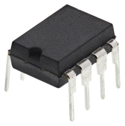
ICGOO电子元器件商城为您提供P82B715P由Texas Instruments设计生产,在icgoo商城现货销售,并且可以通过原厂、代理商等渠道进行代购。 P82B715P价格参考¥6.74-¥13.75。Texas InstrumentsP82B715P封装/规格:接口 - 信号缓冲器,中继器,分配器, Buffer, ReDriver 1 Channel 8-PDIP。您可以下载P82B715P参考资料、Datasheet数据手册功能说明书,资料中有P82B715P 详细功能的应用电路图电压和使用方法及教程。
Texas Instruments(德州仪器)的P82B715P是一款用于接口、信号缓冲器、中继器和分配器的应用器件。它主要用于延长和增强双向数据总线的传输距离与性能,特别是在具有较长电缆或复杂拓扑结构的系统中。

 应用场景:

1. 工业自动化:
   - 在工厂自动化和过程控制中,P82B715P可以用于延长RS-485或CAN总线的距离。这些总线常用于连接传感器、执行器和控制器。通过使用P82B715P,可以确保信号在长距离传输时保持完整性,减少噪声干扰和信号衰减。

2. 楼宇自动化:
   - 楼宇自动化系统(如暖通空调、照明控制和安全系统)通常需要在较大范围内进行通信。P82B715P可以作为信号中继器,确保从中央控制器到各个子系统的信号传输稳定可靠,即使在布线复杂的环境中也能正常工作。

3. 汽车电子:
   - 在现代汽车中,各种电子控制单元(ECU)之间需要高效通信。P82B715P可以用于增强车内网络(如LIN、CAN等)的信号质量,确保数据传输的准确性和实时性,尤其是在多节点通信的情况下。

4. 通信设备:
   - 对于需要长距离通信的设备,如调制解调器、路由器和交换机,P82B715P可以作为信号缓冲器或中继器,确保数据在不同设备之间的传输更加稳定,避免因信号衰减导致的数据丢失或误码。

5. 智能电网:
   - 智能电网中的电力线通信(PLC)和其他通信协议可能需要长距离传输。P82B715P可以帮助增强信号强度,确保电力公司和用户之间的数据交换更加可靠,支持远程抄表、负荷管理和故障检测等功能。

6. 医疗设备:
   - 在医疗设备中,尤其是那些需要高可靠性和低延迟通信的设备(如监护仪、影像设备),P82B715P可以用于确保内部模块之间的信号传输质量,保障设备的正常运行和数据的准确性。

总之,P82B715P适用于任何需要增强信号传输距离和质量的场景,特别是在工业、汽车、通信和医疗等领域,能够有效提高系统的可靠性和性能。
| 参数 | 数值 |
| 产品目录 | 集成电路 (IC)半导体 |
| 描述 | IC REDRIVER I2C 1CH 8DIP接口-信号缓冲器、中继器 I2C Bus Extender |
| 产品分类 | |
| 品牌 | Texas Instruments |
| 产品手册 | |
| 产品图片 |
|
| rohs | 符合RoHS无铅 / 符合限制有害物质指令(RoHS)规范要求 |
| 产品系列 | 接口 IC,接口-信号缓冲器、中继器,Texas Instruments P82B715P- |
| 数据手册 | |
| 产品型号 | P82B715P |
| Tx/Rx类型 | I²C 逻辑 |
| 产品目录页面 | |
| 产品种类 | 接口-信号缓冲器、中继器 |
| 产品类型 | Bus Extenders |
| 传播延迟时间 | 250 ns |
| 供应商器件封装 | 8-PDIP |
| 其它名称 | 296-23469-5 |
| 包装 | 管件 |
| 单位重量 | 440.400 mg |
| 商标 | Texas Instruments |
| 安装类型 | 通孔 |
| 安装风格 | Through Hole |
| 封装 | Tube |
| 封装/外壳 | 8-DIP(0.300",7.62mm) |
| 封装/箱体 | PDIP-8 |
| 工作温度 | -40°C ~ 85°C |
| 工作温度范围 | - 40 C to + 85 C |
| 工作电源电压 | 3 V to 12 V |
| 工厂包装数量 | 50 |
| 应用 | I²C |
| 延迟时间 | - |
| 数据速率(最大值) | - |
| 标准包装 | 50 |
| 电压-电源 | 4.5 V ~ 12 V |
| 电容-输入 | 3000pF |
| 电流-电源 | 22mA |
| 类型 | 缓冲器, 转接驱动器 |
| 系列 | P82B715 |
| 输入 | 2 线式总线 |
| 输出 | 2 线式总线 |
| 通道数 | 1 |
| 逻辑类型 | Bus Extender |


- 商务部:美国ITC正式对集成电路等产品启动337调查
- 曝三星4nm工艺存在良率问题 高通将骁龙8 Gen1或转产台积电
- 太阳诱电将投资9.5亿元在常州建新厂生产MLCC 预计2023年完工
- 英特尔发布欧洲新工厂建设计划 深化IDM 2.0 战略
- 台积电先进制程称霸业界 有大客户加持明年业绩稳了
- 达到5530亿美元!SIA预计今年全球半导体销售额将创下新高
- 英特尔拟将自动驾驶子公司Mobileye上市 估值或超500亿美元
- 三星加码芯片和SET,合并消费电子和移动部门,撤换高东真等 CEO
- 三星电子宣布重大人事变动 还合并消费电子和移动部门
- 海关总署:前11个月进口集成电路产品价值2.52万亿元 增长14.8%


PDF Datasheet 数据手册内容提取
Product Sample & Technical Tools & Support & Folder Buy Documents Software Community P82B715 SCPS145B–DECEMBER2007–REVISEDFEBRUARY2016 2 P82B715 I C Bus Extender 1 Features 2 Applications • OperatingPower-SupplyVoltageRangeof • HDMIDDC 1 3Vto12V • LongI2CCommunications • SupportsBidirectionalDataTransferofI2CBus • IndustrialCommunications Signals • AllowsBusCapacitanceof400pFonMainI2C 3 Description Bus(Sx/SySide)and3000pFonTransmission The P82B715 is a device for buffering highly- Side(Lx/LySide) capacitive I2C bus systems, and it supports bidirectional data transfer through the I2C bus. The • DualBidirectionalUnity-Voltage-GainBufferWith P82B715 buffers both the serial data (SDA) and NoExternalDirectionalControlRequired serial clock (SCL) signals on the I2C bus and allows • Drives10×Lower-ImpedanceBusWiringfor for extension of the I2C bus, while retaining all the ImprovedNoiseImmunity operatingmodesandfeaturesoftheI2Csystem. • Multi-DropDistributionofI2CSignalsUsingLow- CostTwisted-PairCables DeviceInformation(1) • I2CBusOperationOver50MetersofTwisted-Pair PARTNUMBER PACKAGE BODYSIZE(NOM) Wire SOIC(8) 4.90mm×3.91mm P82B715 • Latch-upPerformanceExceeds100mAPer PDIP(8) 9.81mm×6.35mm JESD78,ClassII (1) For all available packages, see the orderable addendum at • ESDProtectionExceedsJESD22 theendofthedatasheet. – 2500-VHuman-BodyModel(A114-A) – 400-VMachineModel(A115-A) – 1000-VCharged-DeviceModel(C101) BlockDiagram V CC P82B715 Sx/SDA Buffer Lx/LDA Sy/SCL Buffer Ly/LCL GND 1 An IMPORTANT NOTICE at the end of this data sheet addresses availability, warranty, changes, use in safety-critical applications, intellectualpropertymattersandotherimportantdisclaimers.PRODUCTIONDATA.
P82B715 SCPS145B–DECEMBER2007–REVISEDFEBRUARY2016 www.ti.com Table of Contents 1 Features.................................................................. 1 8.2 FunctionalBlockDiagram.........................................7 2 Applications........................................................... 1 8.3 FeatureDescription...................................................7 3 Description............................................................. 1 8.4 DeviceFunctionalModes..........................................8 4 RevisionHistory..................................................... 2 9 ApplicationandImplementation.......................... 9 9.1 ApplicationInformation..............................................9 5 PinConfigurationandFunctions......................... 3 9.2 TypicalApplication....................................................9 6 Specifications......................................................... 4 10 PowerSupplyRecommendations..................... 13 6.1 AbsoluteMaximumRatings......................................4 11 Layout................................................................... 13 6.2 ESDRatings..............................................................4 6.3 RecommendedOperatingConditions.......................4 11.1 LayoutGuidelines.................................................13 6.4 ThermalInformation..................................................4 11.2 LayoutExample....................................................13 6.5 ElectricalCharacteristics...........................................5 12 DeviceandDocumentationSupport................. 14 6.6 SwitchingCharacteristics..........................................5 12.1 CommunityResource............................................14 6.7 TypicalCharacteristics..............................................6 12.2 Trademarks...........................................................14 7 ParameterMeasurementInformation..................6 12.3 ElectrostaticDischargeCaution............................14 12.4 Glossary................................................................14 8 DetailedDescription.............................................. 7 13 Mechanical,Packaging,andOrderable 8.1 Overview...................................................................7 Information........................................................... 14 4 Revision History NOTE:Pagenumbersforpreviousrevisionsmaydifferfrompagenumbersinthecurrentversion. ChangesfromRevisionA(February2008)toRevisionB Page • AddedESDRatingstable,FeatureDescriptionsection,DeviceFunctionalModes,ApplicationandImplementation section,PowerSupplyRecommendationssection,Layoutsection,DeviceandDocumentationSupportsection,and Mechanical,Packaging,andOrderableInformationsection ................................................................................................. 1 2 SubmitDocumentationFeedback Copyright©2007–2016,TexasInstrumentsIncorporated ProductFolderLinks:P82B715
P82B715 www.ti.com SCPS145B–DECEMBER2007–REVISEDFEBRUARY2016 5 Pin Configuration and Functions PPackage 8-PinPDIP DPackage TopView 8-PinSOIC TopView NC 1 8 VCC NC 1 8 VCC Lx 2 7 Ly Lx 2 7 Ly Sx 3 6 Sy Sx 3 6 Sy GND 4 5 NC GND 4 5 NC NC–No internal connection PinFunctions PIN I/O DESCRIPTION NO. NAME 1 NC — Noconnection 2 Lx I/O BufferedserialdatabusorLDA 3 Sx I/O SerialdatabusorSDA.ConnecttoV ofI2Cmasterthroughapullupresistor. CC 4 GND — Ground 5 NC — Noconnection 6 Sy I/O SerialclockbusorSCL.ConnecttoV ofI2Cmasterthroughapullupresistor. CC 7 Ly I/O BufferedserialclockbusorLCL 8 V I Supplyvoltage CC Copyright©2007–2016,TexasInstrumentsIncorporated SubmitDocumentationFeedback 3 ProductFolderLinks:P82B715
P82B715 SCPS145B–DECEMBER2007–REVISEDFEBRUARY2016 www.ti.com 6 Specifications 6.1 Absolute Maximum Ratings overoperatingfree-airtemperaturerange(unlessotherwisenoted)(1) MIN MAX UNIT V Supplyvoltage –0.3 12 V CC I2Cbusvoltage SxorSy 0 V CC V V b Bufferedbusvoltage LxorLy 0 V CC SxorSy 60 I Continuousoutputcurrent mA O LxorLy 60 I ContinuouscurrentthroughV orGND 60 mA CC CC T Storagetemperature –55 125 °C stg (1) StressesbeyondthoselistedunderAbsoluteMaximumRatingsmaycausepermanentdamagetothedevice.Thesearestressratings only,whichdonotimplyfunctionaloperationofthedeviceattheseoranyotherconditionsbeyondthoseindicatedunderRecommended OperatingConditions.Exposuretoabsolute-maximum-ratedconditionsforextendedperiodsmayaffectdevicereliability. 6.2 ESD Ratings VALUE UNIT Human-bodymodel(HBM),perANSI/ESDA/JEDECJS-001(1) ±2500 Charged-devicemodel(CDM),perJEDECspecificationJESD22- V(ESD) Electrostaticdischarge C101(2) ±1000 V Machinemodel(MM) ±400 (1) JEDECdocumentJEP155statesthat500-VHBMallowssafemanufacturingwithastandardESDcontrolprocess. (2) JEDECdocumentJEP157statesthat250-VCDMallowssafemanufacturingwithastandardESDcontrolprocess. 6.3 Recommended Operating Conditions MIN MAX UNIT V Supplyvoltage(1) 4.5 12 V CC T Operatingfree-airtemperature –40 85 °C A (1) Operationwithreducedperformanceispossibledownto3V.Typicalstaticsinkingperformanceisnotdegradedat3V,butthedynamic sinkcurrentswhiletheoutputisbeingdriventhroughV /2arereducedandcanincreasefalltimes.Timing-criticaldesignsshould CC accommodatethespecifiedminimums. 6.4 Thermal Information P82B715 THERMALMETRIC(1) D(SOIC) P(PDIP) UNIT 8PINS 8PINS R Junction-to-ambientthermalresistance 105.3 48.9 °C/W θJA R Junction-to-case(top)thermalresistance 51.1 38.1 °C/W θJC(top) R Junction-to-boardthermalresistance 46.2 26.1 °C/W θJB ψ Junction-to-topcharacterizationparameter 8.5 15.4 °C/W JT ψ Junction-to-boardcharacterizationparameter 45.6 26 °C/W JB R Junction-to-case(bottom)thermalresistance N/A N/A °C/W θJC(bot) (1) Formoreinformationabouttraditionalandnewthermalmetrics,seetheSemiconductorandICPackageThermalMetricsapplication report,SPRA953. 4 SubmitDocumentationFeedback Copyright©2007–2016,TexasInstrumentsIncorporated ProductFolderLinks:P82B715
P82B715 www.ti.com SCPS145B–DECEMBER2007–REVISEDFEBRUARY2016 6.5 Electrical Characteristics V =5V,T =25°C,voltagesarespecifiedwithrespecttoGND(unlessotherwisespecified) CC A PARAMETER TESTCONDITIONS MIN TYP MAX UNIT Sx=Sy=V 14 CC V =12V 15 I Quiescentsupplycurrent CC mA CC BothI2Cinputslow, 22 Bothbufferedoutputssinking30mA V >3V, CC I OutputsinkcurrentonI2Cbus Sx,Sy VSx,VSy(low)=0.4V, 2.6 mA IOS V ,V (low)onbufferedbus=0.3V, Lx Ly I ,I =–3mA (1) Lx Ly V ,V (low)=0.4V, VLx,VLy (low)onI2Cbus=0.3V 30 Sx Sy 3V<V <4.5V, CC Outputsinkcurrentonbuffered V ,V (low)=0.4Vto1.5V, 24 IIOL bus Lx,Ly I Lx,I LysinkingonI2Cbus<–4mA mA Sx Sy 3V<V <4.5V, CC V ,V (low)=1.5VtoV , 24 Lx Ly CC I ,I sinkingonI2Cbus=–7mA Sx Sy InputcurrentfromI2Cbus Sx,Sy I ,I sinkonbufferedbus=30mA –3.2 Lx Ly Inputcurrentfrombufferedbus(1) VI C,CI>3siVn,konI2Cbus=3mA(1) –3 mA I Sx Sy I Lx,Ly V =3Vto12V, CC Leakagecurrentonbufferedbus V ,V =V , 200 μA Lx Ly CC V ,V =V Sx Sy CC Z /Z Input/outputimpedance V <V ,Bufferisactive 8 10 13 in out Sx Lx (1) Bufferispassiveinthistest.TheSx/SysinkcurrentflowsthroughaninternalresistortothedriverconnectedattheLx/LyI/O. 6.6 Switching Characteristics V =5V,T =25°C,nocapacitiveloads,voltagesarespecifiedwithrespecttoGND(unlessotherwisespecified) CC A FROM TO PARAMETER TESTCONDITIONS MIN TYP MAX UNIT (INPUT) (OUTPUT) BUFFERDELAYTIMES DelaytimetoV voltagecrossingV /2for inputdrivecurreLnxtstepI atSx(1)(sCeCe R pullup=270Ω ISx VLx 250 ns Sx Lx I V Figure2) Sy Ly t rise/fall Bufferdelaytime,switchingedgesbetween V V V inputand R pullup=4700Ω Lx Sx 0 ns VLx output(2) Lx VLy VSy Sx (1) Aconventionalinput-outputdelayisnotobservedintheSx/Lxvoltagewaveforms,becausetheinputandoutputpinsareinternallytied witha30-Ωresistorsotheyshowequallogicvoltagelevelstowithin100mV.WhenconnectedinanI2Csystem,anSx/Syinputpin cannotrise/falluntilthebufferedbusloadattheoutputpinhasbeendrivenbytheinternalamplifier.Thistestmeasuresthebus propagationdelaycausedtofallingorrisingvoltagesattheLx/Lyoutput(aswellastheSx/Syinput)bytheamplifier’sresponsetime. ThefiguregivenismeasuredwithadrivecurrentasshowninFigure2.Becausethisisadynamicbustestinwhichacorresponding busdrivingIChasanoutputvoltagewellabove0.4V,6mAisusedinsteadofthestatic3mA. (2) ThesignalpathLxtoSxandLytoSyispassivethroughtheinternal30-Ωresistor.Thereisnoamplifierinvolvedandessentiallyno signalpropagationdelay. Copyright©2007–2016,TexasInstrumentsIncorporated SubmitDocumentationFeedback 5 ProductFolderLinks:P82B715
P82B715 SCPS145B–DECEMBER2007–REVISEDFEBRUARY2016 www.ti.com 6.7 Typical Characteristics 0.2 0.15 V) (OL 0.1 V 0.05 0 0 5 10 15 20 25 30 ILX (mA) D001 Figure1. TypicalV ofLx/Ly(R onSx=4.7kΩ,T =25C,V =0V) OL PU A SX 7 Parameter Measurement Information 5 V Input Current 4.7 kΩ 270Ω 4.7 kΩ Sx Lx Lx Sx 5 V P82B715 P82B715 Input Output Input and Output Voltage 0 V I = 6 mA t t d d Figure2. TestCircuitforDelayTimes 6 SubmitDocumentationFeedback Copyright©2007–2016,TexasInstrumentsIncorporated ProductFolderLinks:P82B715
P82B715 www.ti.com SCPS145B–DECEMBER2007–REVISEDFEBRUARY2016 8 Detailed Description 8.1 Overview The I2C bus capacitance limit of 400 pF restricts practical communication distances to a few meters. One of the advantages of the P82B715 is that it can isolate bus capacitance such that the total loading (devices, connectors, traces and wires) of the new bus or remote I2C nodes are not apparent to other I2C buses (or nodes). This is achieved by using one P82B715 device at each end of a long cable. The pin Lx of one P82B715 device must be connected to Lx of the second P82B715 (similarly for Ly). This allows the total system capacitance load to be around 3000 pF. The P82B715 uses unidirectional analog current amplification to increase the current sink capability of I2C chips to change the 400-pF I2C bus specification limit into a 3-nF bus wiring capacitance limit. That means longer cables or lower-cost general-purpose wiring may be used to connect two separate I2C-based systems, without worrying about the special voltage levels associated with other I2C bus buffers. Multiple P82B715s can be connected together in a star or multipoint architecture by their Lx/Ly ports, without limit, as long as the total capacitance of the system remains less than about 3000 pF (400 pF or less when referenced to any Sx/Sy connection). In that arrangement, the master and/or slave devices are attached to the Sx/Sy port of each P82B715. In normal use, the power-supply voltages at each end of the low-impedance bufferedbuslineshouldbethesame.Ifthesedifferbyasignificantamount,noisemarginissacrificed. TwoormoreSxorSyI/Oscanbeinterconnectedandarealsofullycompatiblewithbusbuffersthatusevoltage- leveloffsets(suchastheTCA9517)becauseitduplicatesandtransmitstheoffsetvoltage. 8.2 Functional Block Diagram V CC P82B715 Sx/SDA Buffer Lx/LDA Sy/SCL Buffer Ly/LCL GND 8.3 Feature Description 8.3.1 SxandSy The I2C pins (Sx and Sy) are designed to interface with a normal I2C bus. The maximum I2C bus supply voltage is12V.TheSxandSypinscontainidenticalcircuitryandcanbeusedinterchangeablyasSCLorSDA. 8.3.2 LxandLy The Lx and Ly pins are designed to interface with the high capacitance bus. This port of the device features circuitry to assist in sinking large amounts of currents required to operate a large capacitance bus at high speeds.MoreonthiscircuitrycanbefoundinLx/LyBufferedBusCircuitry. 8.3.3 Lx/LyBufferedBusCircuitry On the special low-impedance or buffered-line side, the corresponding output becomes the LDA data line or LCL clock line. The P82B715 provides current amplification from its I2C bus to its low impedance or buffered bus. Whenever current is flowing out of Sx into an I2C chip driving the I2C bus low, its amplifier sinks ten times that current into Lx, to drive the buffered bus low (see Figure 3). To minimize interference and ensure stability, the current rise and fall times of the Lx drive amplifier are internally controlled. The P82B715 does not amplify signal Copyright©2007–2016,TexasInstrumentsIncorporated SubmitDocumentationFeedback 7 ProductFolderLinks:P82B715
P82B715 SCPS145B–DECEMBER2007–REVISEDFEBRUARY2016 www.ti.com Feature Description (continued) currents flowing into Sx on the I2C bus driven by currents flowing out of Lx on the buffered side. A buffered bus logic low signal at Lx passes through the internal 30-Ω resistor to drive the I2C bus low. This signal current amplification, dependent on its direction, preserves the multi-master bidirectional open-collector/open-drain characteristicofanyconnectedI2Cbuslinesandthenewlow-impedancebus.Buslogic-signalvoltagelevelsare clampedat(V +0.7V)but,otherwise,areindependentofthesupplyvoltage,V . CC CC I = I Sx Lx I I I = 10´I Sx Current Sx Lx Sx I2C Bus Sx Lx Buffered Bus Sense 30W 9´I Sx V CC + – GND Figure3. EquivalentCircuit(One-HalfofP82B715) 8.4 Device Functional Modes TheP82B715hastwomodeswhenpowered,whichdependonthestateoftheI2Cbus. 8.4.1 IdleBus WhentheI2Cbusisidleandhigh,littleornocurrentflowsthroughthedevice.Inthiscase,theLx/Lybufferisnot turnedon. 8.4.2 Active-LowBus When a device connected to the Sx / Sy side of the device is transmitting a 0, a large amount of current will flow throughtheP82B715,whichactivatestheinternalpulldowntoassistwiththelargecapacitance. 8 SubmitDocumentationFeedback Copyright©2007–2016,TexasInstrumentsIncorporated ProductFolderLinks:P82B715
P82B715 www.ti.com SCPS145B–DECEMBER2007–REVISEDFEBRUARY2016 9 Application and Implementation NOTE Information in the following applications sections is not part of the TI component specification, and TI does not warrant its accuracy or completeness. TI’s customers are responsible for determining suitability of components for their purposes. Customers should validateandtesttheirdesignimplementationtoconfirmsystemfunctionality. 9.1 Application Information The P82B715 can operate with a supply voltage from 3 V to 12 V, but the logic-signal levels at Sx/Lx are independent of the supply voltage. They remain at the levels presented to the chip by the attached devices. The maximum static I2C bus sink current, 3 mA, flowing in either direction in the internal current sense resistor, causes a difference less than 100 mV in the bus logic low levels at Sx and Lx. This makes P82B715 fully compatible with all logic signal drivers, including TTL. The P82B715 cannot modify the bus logic signal voltage levels, but it contains internal diodes connected between Lx/Sx and V that conduct and limit the logic signal CC swingiftheappliedlogiclevelswouldhaveexceededthesupplyvoltagebymorethan0.7V. In normal applications, external pullup resistors pull the connected buses up to the desired voltage high level. Usually this is the supply voltage, V , but for very low logic voltages, it is necessary to use a V of at least CC CC 3.3 V and preferably higher. Note that full performance over temperature is ensured only from 4.5 V. Specificationderatingsapplywhenitssupplyvoltageisreducedbelow4.5V.TheabsoluteminimumV is3V. CC 9.2 Typical Application By using two (or more) P82B715 devices, a subsystem can be built that retains the interface characteristics of a normalI2Cdevicesothatthesubsystemmaybeincludedin,oraddedto,anyI2Correlatedsystem. The subsystem features a low-impedance or buffered bus capable of driving large wiring capacitance (see Figure4). V CC P82B715 P82B715 LDA SDA SDA ½ ½ Long I2C Cable Device LCL SCL SCL ½ ½ Standard Special Special Standard I2C Bus Buffered Buffered I2C Bus Bus Bus Figure4. MinimumSubsystemDiagram 9.2.1 DesignRequirements Table1liststhedesignparametersforthisexample. Table1.DesignParameters PARAMETER DESCRIPTION VALUE V SupplyVoltage 3.3V CC C CapacitanceontheLx/Lybus 3000pF Lx R PullupresistorfortheSx/Sybus 4700Ω PU_Sx R PullupresistorfortheLx/Lybus 330Ω PU_Lx Copyright©2007–2016,TexasInstrumentsIncorporated SubmitDocumentationFeedback 9 ProductFolderLinks:P82B715
P82B715 SCPS145B–DECEMBER2007–REVISEDFEBRUARY2016 www.ti.com 9.2.2 DetailedDesignProcedure 9.2.2.1 I2CSystems As in standard I2C systems, pullup resistors are required to provide the logic high levels on the buffered bus, as the standard open-collector configuration is retained. The size and number of pullup resistors depends on the system. If P82B715 devices are to be permanently connected into a system, the circuit may be configured with only one pullup resistor on the buffered bus and none on the I2C buses, but the system design is simplified, and performance is improved by fitting separate pullups on each section of the bus. When a subsystem using P82B715 may be optionally connected to an existing I2C system that already has a pullup, the effects of the subsystempullupsactinginparallelwiththeexistingI2Cbuspullupmustbeconsidered. 9.2.2.2 PullupResistanceCalculation When calculating the pullup resistance values, the gain of the buffer introduces scaling factors that must be applied to the system components. In practical systems, the pullup resistance value is calculated to meet the rise time limit for I2C systems. As an approximation, this limit is satisfied in a 100-kHz system if the time constant of thetotalsystem(productofthenetresistanceandnetcapacitance)issetto1 μsorless. In systems using the P82B715, it is convenient to set the total system time constant by considering each bus node separately (that is, the I2C nodes and the buffered bus node) and selecting a separate pullup resistor for each node to provide time constants of less than 1 μs. If each node complies then the system requirement is alsomet. Thisarrangement,usingmultiplepullupsasshowninFigure5,providesthebestsystemperformanceandallows stand-alone operation of individual I2C buses if parts of the extended system are disconnected or reconnected. Foreachbussection,thepullupresistoriscalculatedas: R=1μs/(C +C ) device wiring where • C =Sumofanyconnecteddevicecapacitances device • C =Totalwiringandstraycapacitanceonthebussection (1) wiring The 1 μs is an approximation with a safety factor to the theoretical time constant necessary to meet the specified 1-μs bus rise-time specification in a system with variable logic thresholds, where the CMOS limits of 30% and 70%ofV apply.Thecalculatedvalueis1.18 μs. CC If these capacitances cannot be measured or calculated, an approximation can be made by assuming that each device presents 10 pF of load capacitance and 10 pF of trace capacitance, and that cables range from 50 pF to 100pFpermeter. V = 5 V CC R1 R2 R3 SDA SDA Sx Lx Lx Sx I2C 1 Buffered Bus I2C 2 SCL SCL Sy Ly Ly Sy V = 5 V CC R4 SDA Lx Sx I2C 3 SCL Ly Sy Figure5. SinglePullupBufferedBus If only a single pullup is used, it must be placed on the buffered bus (as R2 in Figure 5) and the associated total system capacitance calculated by combining the individual bus capacitances into an equivalent capacitive loadingonthebufferedbus. 10 SubmitDocumentationFeedback Copyright©2007–2016,TexasInstrumentsIncorporated ProductFolderLinks:P82B715
P82B715 www.ti.com SCPS145B–DECEMBER2007–REVISEDFEBRUARY2016 This equivalent capacitance is the sum of the capacitance on the buffered bus plus ten times the sum of the capacitances on all the connected I2C nodes. The calculated value should not exceed 4 nF. The single buffered bus pullup resistor is then calculated to achieve the 1-μs rise time, and it provides the pullup for the buffered bus andforallotherconnectedI2Cbusnodesincludedinthecalculation. 9.2.2.3 CalculatingBusDriveCurrents Figure 5 shows three P82B715 devices connected to a common buffered bus. The associated bus capacitances are omitted for clarity, but assume the resistors have been selected to give R-C products of less than 1 μs so the bus rise-time requirement is satisfied. An I2C device connected at I2C 1 and holding the SDA bus low must sink the current flowing in its local pullup R1, plus, with assistance from the P82B715, the currents in R2, R3, and R4. Because the resistors R3 and R4 act to pull the bus nodes I2C 2 and I2C 3 and their corresponding Sx pins to a voltage higher than the voltage at the Lx pins, their buffer amplifiers are inactive. The SDA at Sx of I2C 2 and I2C 3 is pulled low by the low at Lx through the internal 30-Ω resistor that links Lx to Sx. So the effective current that must be sunk by the P82B715 buffer on I2C 1 at its Lx pin is the sum of the currents in R2, R3, and R4. The Sx current that must be sunk by an I2C device at I2C 1 due to the buffer gain action is 1/10 of the Lx current. So the effective pullup determining the current to be sunk by an I2C device at I2C 1 is R1 in parallel with resistors ten timesthevaluesofR2,R3,andR4.IfR1=R3=R4=10kΩ,andR2=1kΩ,theeffectivepulluploadatI2C1is 10kΩ||10kΩ||100kΩ||100kΩ =4.55kΩ. ThesamecalculationappliesforI2C2orI2C3. To calculate the current sunk by the Lx pin of the buffer at I2C 1, note that the current in R1 is sunk directly by the device at I2C 1. The buffer, therefore, sinks only the currents flowing in R2, R3, and R4, so the effective pullupisR2inparallelwithR3andR4. In this example that is 1 kΩ||10 kΩ||10 kΩ = 833 Ω. For a 5.5-V supply and 0.4-V low, the buffer is sinking 16.3mA. The P82B715 has a static sink rating of 30 mA at Lx. The requirement is that the pullup on the buffered bus, in parallel with all other pullups that it is indirectly pulling low on Sx pins of other P82B715 devices, does not cause this30-mAlimittobeexceeded. Theminimumpullupresistanceina5-V± 10%systemis170 Ω. Thegeneralrequirementis: (V (max)–0.4)/R <30mA CC P where • R =ParallelcombinationofallpullupresistorsdrivenbytheLxpinoftheP82B715 (2) p Figure6 showscalculationsforanexpandedI2Cbuswith3nFofcablecapacitance. Copyright©2007–2016,TexasInstrumentsIncorporated SubmitDocumentationFeedback 11 ProductFolderLinks:P82B715
P82B715 SCPS145B–DECEMBER2007–REVISEDFEBRUARY2016 www.ti.com Local Bus Proposed Bus Expansion V 5 V CC R1 R2 R3 SDA I2C Sx Lx LDA SDA I2C Lx Sx I2C SDA 3 nF = Cable Wiring Capacitance GND 0 V Effective Capacitance Effective Capacitance Effective Capacitance Local Bus I2C Devices Buffered Line Remote I2C Devices 2×I2C Devices 20 pF 1×I2C Devices 10 pF Wiring Capacitance 3000 pF Strays 20 pF Strays 10 pF P82B715 10 pF P82B715 10 pF Total 3000 pF Total 50 pF Total 30 pF Local I2C Pullup Buffered Bus Pullup Remote I2C Pullup 1µs 1µs 1µs R1= = 20kΩ R2= = 330Ω R3= = 33kΩ 50pF 3000pF 30pF Figure6. TypicalLoadingCalculations 9.2.3 ApplicationCurve 3.5 Lx/Ly Sx/Sy 3 2.5 e (V) 2 g a olt 1.5 V 1 0.5 0 Time D002 Figure7. VoltageOnBus(3000pFonLx/LyWithR =330Ω) PU 12 SubmitDocumentationFeedback Copyright©2007–2016,TexasInstrumentsIncorporated ProductFolderLinks:P82B715
P82B715 www.ti.com SCPS145B–DECEMBER2007–REVISEDFEBRUARY2016 10 Power Supply Recommendations The P82B715 power supply requirements can be see in the Recommended Operating Conditions. Note that the P82B715canoperatedownto3V,butatreducedperformance. 11 Layout 11.1 Layout Guidelines General layout best practices are recommended. It is common to have a dedicated ground plane on an inner layer of the board, and pins that are connected to ground must have a low-impedance path to the ground place intheformofwidepolygonpours,andmultiplevias. Bypass and decoupling capacitors are commonly used to control the voltage on the VCC pin, using a larger capacitor to provide additional power in the event of a short power supply glitch (typically 1 μF), and a smaller capacitor(typically0.1μF)tofilterouthigh-frequencyripple. 11.2 Layout Example = VIA to ground plane To high-capacitance bus 0603 Cap NC V CC Lx Ly Sx Sy GND NC To low-capacitance bus Figure8. DPackageExampleLayout Copyright©2007–2016,TexasInstrumentsIncorporated SubmitDocumentationFeedback 13 ProductFolderLinks:P82B715
P82B715 SCPS145B–DECEMBER2007–REVISEDFEBRUARY2016 www.ti.com 12 Device and Documentation Support 12.1 Community Resource The following links connect to TI community resources. Linked contents are provided "AS IS" by the respective contributors. They do not constitute TI specifications and do not necessarily reflect TI's views; see TI's Terms of Use. TIE2E™OnlineCommunity TI'sEngineer-to-Engineer(E2E)Community.Createdtofostercollaboration amongengineers.Ate2e.ti.com,youcanaskquestions,shareknowledge,exploreideasandhelp solveproblemswithfellowengineers. DesignSupport TI'sDesignSupport QuicklyfindhelpfulE2Eforumsalongwithdesignsupporttoolsand contactinformationfortechnicalsupport. 12.2 Trademarks E2EisatrademarkofTexasInstruments. Allothertrademarksarethepropertyoftheirrespectiveowners. 12.3 Electrostatic Discharge Caution Thesedeviceshavelimitedbuilt-inESDprotection.Theleadsshouldbeshortedtogetherorthedeviceplacedinconductivefoam duringstorageorhandlingtopreventelectrostaticdamagetotheMOSgates. 12.4 Glossary SLYZ022—TIGlossary. Thisglossarylistsandexplainsterms,acronyms,anddefinitions. 13 Mechanical, Packaging, and Orderable Information The following pages include mechanical, packaging, and orderable information. This information is the most current data available for the designated devices. This data is subject to change without notice and revision of thisdocument.Forbrowser-basedversionsofthisdatasheet,refertotheleft-handnavigation. 14 SubmitDocumentationFeedback Copyright©2007–2016,TexasInstrumentsIncorporated ProductFolderLinks:P82B715
PACKAGE OPTION ADDENDUM www.ti.com 6-Feb-2020 PACKAGING INFORMATION Orderable Device Status Package Type Package Pins Package Eco Plan Lead/Ball Finish MSL Peak Temp Op Temp (°C) Device Marking Samples (1) Drawing Qty (2) (6) (3) (4/5) P82B715D ACTIVE SOIC D 8 75 Green (RoHS NIPDAU Level-1-260C-UNLIM -40 to 85 PG715 & no Sb/Br) P82B715DG4 ACTIVE SOIC D 8 75 Green (RoHS NIPDAU Level-1-260C-UNLIM -40 to 85 PG715 & no Sb/Br) P82B715DR ACTIVE SOIC D 8 2500 Green (RoHS NIPDAU Level-1-260C-UNLIM -40 to 85 PG715 & no Sb/Br) P82B715DRG4 ACTIVE SOIC D 8 2500 Green (RoHS NIPDAU Level-1-260C-UNLIM -40 to 85 PG715 & no Sb/Br) P82B715P ACTIVE PDIP P 8 50 Pb-Free NIPDAU N / A for Pkg Type -40 to 85 P82B715P (RoHS) P82B715PE4 ACTIVE PDIP P 8 50 Pb-Free NIPDAU N / A for Pkg Type -40 to 85 P82B715P (RoHS) (1) The marketing status values are defined as follows: ACTIVE: Product device recommended for new designs. LIFEBUY: TI has announced that the device will be discontinued, and a lifetime-buy period is in effect. NRND: Not recommended for new designs. Device is in production to support existing customers, but TI does not recommend using this part in a new design. PREVIEW: Device has been announced but is not in production. Samples may or may not be available. OBSOLETE: TI has discontinued the production of the device. (2) RoHS: TI defines "RoHS" to mean semiconductor products that are compliant with the current EU RoHS requirements for all 10 RoHS substances, including the requirement that RoHS substance do not exceed 0.1% by weight in homogeneous materials. Where designed to be soldered at high temperatures, "RoHS" products are suitable for use in specified lead-free processes. TI may reference these types of products as "Pb-Free". RoHS Exempt: TI defines "RoHS Exempt" to mean products that contain lead but are compliant with EU RoHS pursuant to a specific EU RoHS exemption. Green: TI defines "Green" to mean the content of Chlorine (Cl) and Bromine (Br) based flame retardants meet JS709B low halogen requirements of <=1000ppm threshold. Antimony trioxide based flame retardants must also meet the <=1000ppm threshold requirement. (3) MSL, Peak Temp. - The Moisture Sensitivity Level rating according to the JEDEC industry standard classifications, and peak solder temperature. (4) There may be additional marking, which relates to the logo, the lot trace code information, or the environmental category on the device. (5) Multiple Device Markings will be inside parentheses. Only one Device Marking contained in parentheses and separated by a "~" will appear on a device. If a line is indented then it is a continuation of the previous line and the two combined represent the entire Device Marking for that device. Addendum-Page 1
PACKAGE OPTION ADDENDUM www.ti.com 6-Feb-2020 (6) Lead/Ball Finish - Orderable Devices may have multiple material finish options. Finish options are separated by a vertical ruled line. Lead/Ball Finish values may wrap to two lines if the finish value exceeds the maximum column width. Important Information and Disclaimer:The information provided on this page represents TI's knowledge and belief as of the date that it is provided. TI bases its knowledge and belief on information provided by third parties, and makes no representation or warranty as to the accuracy of such information. Efforts are underway to better integrate information from third parties. TI has taken and continues to take reasonable steps to provide representative and accurate information but may not have conducted destructive testing or chemical analysis on incoming materials and chemicals. TI and TI suppliers consider certain information to be proprietary, and thus CAS numbers and other limited information may not be available for release. In no event shall TI's liability arising out of such information exceed the total purchase price of the TI part(s) at issue in this document sold by TI to Customer on an annual basis. Addendum-Page 2
PACKAGE MATERIALS INFORMATION www.ti.com 21-Jan-2016 TAPE AND REEL INFORMATION *Alldimensionsarenominal Device Package Package Pins SPQ Reel Reel A0 B0 K0 P1 W Pin1 Type Drawing Diameter Width (mm) (mm) (mm) (mm) (mm) Quadrant (mm) W1(mm) P82B715DR SOIC D 8 2500 330.0 12.4 6.4 5.2 2.1 8.0 12.0 Q1 PackMaterials-Page1
PACKAGE MATERIALS INFORMATION www.ti.com 21-Jan-2016 *Alldimensionsarenominal Device PackageType PackageDrawing Pins SPQ Length(mm) Width(mm) Height(mm) P82B715DR SOIC D 8 2500 367.0 367.0 35.0 PackMaterials-Page2
PACKAGE OUTLINE D0008A SOIC - 1.75 mm max height SCALE 2.800 SMALL OUTLINE INTEGRATED CIRCUIT C SEATING PLANE .228-.244 TYP [5.80-6.19] .004 [0.1] C A PIN 1 ID AREA 6X .050 [1.27] 8 1 2X .189-.197 [4.81-5.00] .150 NOTE 3 [3.81] 4X (0 -15 ) 4 5 8X .012-.020 B .150-.157 [0.31-0.51] .069 MAX [3.81-3.98] .010 [0.25] C A B [1.75] NOTE 4 .005-.010 TYP [0.13-0.25] 4X (0 -15 ) SEE DETAIL A .010 [0.25] .004-.010 0 - 8 [0.11-0.25] .016-.050 [0.41-1.27] DETAIL A (.041) TYPICAL [1.04] 4214825/C 02/2019 NOTES: 1. Linear dimensions are in inches [millimeters]. Dimensions in parenthesis are for reference only. Controlling dimensions are in inches. Dimensioning and tolerancing per ASME Y14.5M. 2. This drawing is subject to change without notice. 3. This dimension does not include mold flash, protrusions, or gate burrs. Mold flash, protrusions, or gate burrs shall not exceed .006 [0.15] per side. 4. This dimension does not include interlead flash. 5. Reference JEDEC registration MS-012, variation AA. www.ti.com
EXAMPLE BOARD LAYOUT D0008A SOIC - 1.75 mm max height SMALL OUTLINE INTEGRATED CIRCUIT 8X (.061 ) [1.55] SYMM SEE DETAILS 1 8 8X (.024) [0.6] SYMM (R.002 ) TYP [0.05] 5 4 6X (.050 ) [1.27] (.213) [5.4] LAND PATTERN EXAMPLE EXPOSED METAL SHOWN SCALE:8X SOLDER MASK SOLDER MASK METAL OPENING OPENING METAL UNDER SOLDER MASK EXPOSED METAL EXPOSED METAL .0028 MAX .0028 MIN [0.07] [0.07] ALL AROUND ALL AROUND NON SOLDER MASK SOLDER MASK DEFINED DEFINED SOLDER MASK DETAILS 4214825/C 02/2019 NOTES: (continued) 6. Publication IPC-7351 may have alternate designs. 7. Solder mask tolerances between and around signal pads can vary based on board fabrication site. www.ti.com
EXAMPLE STENCIL DESIGN D0008A SOIC - 1.75 mm max height SMALL OUTLINE INTEGRATED CIRCUIT 8X (.061 ) [1.55] SYMM 1 8 8X (.024) [0.6] SYMM (R.002 ) TYP [0.05] 5 4 6X (.050 ) [1.27] (.213) [5.4] SOLDER PASTE EXAMPLE BASED ON .005 INCH [0.125 MM] THICK STENCIL SCALE:8X 4214825/C 02/2019 NOTES: (continued) 8. Laser cutting apertures with trapezoidal walls and rounded corners may offer better paste release. IPC-7525 may have alternate design recommendations. 9. Board assembly site may have different recommendations for stencil design. www.ti.com
None
IMPORTANTNOTICEANDDISCLAIMER TI PROVIDES TECHNICAL AND RELIABILITY DATA (INCLUDING DATASHEETS), DESIGN RESOURCES (INCLUDING REFERENCE DESIGNS), APPLICATION OR OTHER DESIGN ADVICE, WEB TOOLS, SAFETY INFORMATION, AND OTHER RESOURCES “AS IS” AND WITH ALL FAULTS, AND DISCLAIMS ALL WARRANTIES, EXPRESS AND IMPLIED, INCLUDING WITHOUT LIMITATION ANY IMPLIED WARRANTIES OF MERCHANTABILITY, FITNESS FOR A PARTICULAR PURPOSE OR NON-INFRINGEMENT OF THIRD PARTY INTELLECTUAL PROPERTY RIGHTS. These resources are intended for skilled developers designing with TI products. You are solely responsible for (1) selecting the appropriate TI products for your application, (2) designing, validating and testing your application, and (3) ensuring your application meets applicable standards, and any other safety, security, or other requirements. These resources are subject to change without notice. TI grants you permission to use these resources only for development of an application that uses the TI products described in the resource. Other reproduction and display of these resources is prohibited. No license is granted to any other TI intellectual property right or to any third party intellectual property right. TI disclaims responsibility for, and you will fully indemnify TI and its representatives against, any claims, damages, costs, losses, and liabilities arising out of your use of these resources. TI’s products are provided subject to TI’s Terms of Sale (www.ti.com/legal/termsofsale.html) or other applicable terms available either on ti.com or provided in conjunction with such TI products. TI’s provision of these resources does not expand or otherwise alter TI’s applicable warranties or warranty disclaimers for TI products. Mailing Address: Texas Instruments, Post Office Box 655303, Dallas, Texas 75265 Copyright © 2020, Texas Instruments Incorporated