ICGOO在线商城 > P6SMB150AT3G

 Datasheet下载
- 型号: P6SMB150AT3G
- 制造商: ON Semiconductor
- 库位|库存: xxxx|xxxx
- 要求:
| 数量阶梯 | 香港交货 | 国内含税 |
| +xxxx | $xxxx | ¥xxxx |
查看当月历史价格
查看今年历史价格
P6SMB150AT3G产品简介:
ICGOO电子元器件商城为您提供P6SMB150AT3G由ON Semiconductor设计生产,在icgoo商城现货销售,并且可以通过原厂、代理商等渠道进行代购。 提供P6SMB150AT3G价格参考¥询价-¥询价以及ON SemiconductorP6SMB150AT3G封装/规格参数等产品信息。 你可以下载P6SMB150AT3G参考资料、Datasheet数据手册功能说明书, 资料中有P6SMB150AT3G详细功能的应用电路图电压和使用方法及教程。
| 参数 | 数值 |
| 产品目录 | |
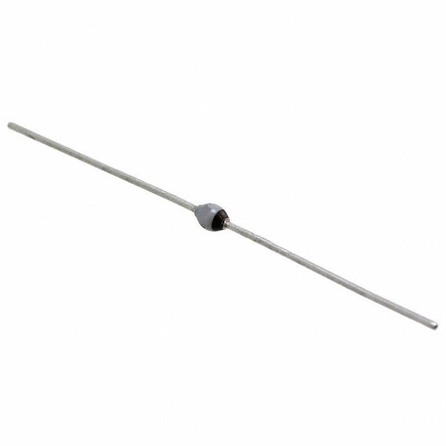
| 描述 | TVS DIODE 128VWM 207VC SMBTVS 二极管 - 瞬态电压抑制器 150V 600W Unidirectional |
| 产品分类 | |
| 品牌 | ON Semiconductor |
| 产品手册 | |
| 产品图片 |
|
| rohs | 符合RoHS无铅 / 符合限制有害物质指令(RoHS)规范要求 |
| 产品系列 | 二极管与整流器,TVS二极管,TVS 二极管 - 瞬态电压抑制器,ON Semiconductor P6SMB150AT3G- |
| 数据手册 | |
| 产品型号 | P6SMB150AT3G |
| PCN组件/产地 | |
| 不同频率时的电容 | 150pF @ 1MHz |
| 产品种类 | Diodes- TVS |
| 供应商器件封装 | SMB |
| 其它名称 | P6SMB150AT3GOS |
| 击穿电压 | 150 V |
| 功率-峰值脉冲 | 600W |
| 包装 | 带卷 (TR) |
| 单向通道 | 1 |
| 双向通道 | - |
| 商标 | ON Semiconductor |
| 安装类型 | 表面贴装 |
| 安装风格 | SMD/SMT |
| 封装 | Reel |
| 封装/外壳 | DO-214AA,SMB |
| 封装/箱体 | DO-214AA |
| 尺寸 | 3.56 mm W x 4.32 mm L |
| 峰值浪涌电流 | 2.9 A |
| 峰值脉冲功率耗散 | 600 W |
| 工作温度 | -65°C ~ 150°C (TJ) |
| 工作电压 | 128 V |
| 工厂包装数量 | 2500 |
| 应用 | 通用 |
| 最大工作温度 | + 150 C |
| 最小工作温度 | - 65 C |
| 极性 | Unidirectional |
| 标准包装 | 2,500 |
| 电压-击穿(最小值) | 143V |
| 电压-反向关态(典型值) | 128V |
| 电压-箝位(最大值)@Ipp | 207V |
| 电流-峰值脉冲(10/1000µs) | 2.9A (8/20µs) |
| 电源线路保护 | 无 |
| 端接类型 | SMD/SMT |
| 类型 | 齐纳 |
| 系列 | P6SMB6.8AT3G |
| 钳位电压 | 207 V |


- 商务部:美国ITC正式对集成电路等产品启动337调查
- 曝三星4nm工艺存在良率问题 高通将骁龙8 Gen1或转产台积电
- 太阳诱电将投资9.5亿元在常州建新厂生产MLCC 预计2023年完工
- 英特尔发布欧洲新工厂建设计划 深化IDM 2.0 战略
- 台积电先进制程称霸业界 有大客户加持明年业绩稳了
- 达到5530亿美元!SIA预计今年全球半导体销售额将创下新高
- 英特尔拟将自动驾驶子公司Mobileye上市 估值或超500亿美元
- 三星加码芯片和SET,合并消费电子和移动部门,撤换高东真等 CEO
- 三星电子宣布重大人事变动 还合并消费电子和移动部门
- 海关总署:前11个月进口集成电路产品价值2.52万亿元 增长14.8%


PDF Datasheet 数据手册内容提取
P6SMB6.8AT3G Series, SZP6SMB6.8AT3G Series 600 Watt Peak Power Zener Transient Voltage Littelfuse.com Suppressors Unidirectional* PLASTIC SURFACE MOUNT The SMB series is designed to protect voltage sensitive ZENER OVERVOLTAGE components from high voltage, high energy transients. They have TRANSIENT SUPPRESSORS excellent clamping capability, high surge capability, low zener impedance and fast response time. The SMB series is supplied in 5.8−171 VOLTS the Littelfuse exclusive, cost-effective, highly reliable 600 WATT PEAK POWER package and is ideally suited for use in communication systems, automotive, numerical controls, process controls, medical equipment, business machines, power supplies and many other industrial/consumer applications. SMB CASE 403A Specification Features: PLASTIC • Working Peak Reverse Voltage Range − 5.8 to 171 V • Standard Zener Breakdown Voltage Range − 6.8 to 200 V • Peak Power − 600 W @ 1 ms Cathode Anode • ESD Rating of Class 3 (> 16 kV) per Human Body Model • MARKING DIAGRAM Maximum Clamp Voltage @ Peak Pulse Current • Low Leakage < 5 (cid:2)A Above 10 V • UL 497B for Isolated Loop Circuit Protection • Response Time is Typically < 1 ns AYWW • xx (cid:2) SZ Prefix for Automotive and Other Applications Requiring Unique (cid:2) Site and Control Change Requirements; AEC−Q101 Qualified and PPAP Capable • These Devices are Pb−Free and are RoHS Compliant A = Assembly Location Y = Year Mechanical Characteristics: WW = Work Week CASE: Void-free, transfer-molded, thermosetting plastic xx = Device Code (Refer to page 3) FINISH: All external surfaces are corrosion resistant and leads are (cid:2) = Pb−Free Package readily solderable (Note: Microdot may be in either location) MAXIMUM CASE TEMPERATURE FOR SOLDERING PURPOSES: 260°C for 10 Seconds ORDERING INFORMATION LEADS: Modified L−Bend providing more contact area to bond pads Device Package Shipping POLARITY: Cathode indicated by polarity band MOUNTING POSITION: Any P6SMBxxxAT3G SMB 2,500 / (Pb−Free) Tape & Reel SZP6SMBxxxAT3G SMB 2,500 / (Pb−Free) Tape & Reel *Please see P6SMB11CAT3 to P6SMB91CAT3 for Bidirectional devices. Specifications subject to change without notice. © 2016 Littelfuse, Inc. 1 Publication Order Number: September 19, 2016 − Rev. 14 P6SMB6.8AT3/D
P6SMB6.8AT3G Series, SZP6SMB6.8AT3G Series MAXIMUM RATINGS Rating Symbol Value Unit Peak Power Dissipation (Note 1) @ TL = 25°C, Pulse Width = 1 ms PPK 600 W DC Power Dissipation @ TL = 75°C Measured Zero Lead Length (Note 2) PD 3.0 W Derate Above 75°C 40 mW/°C Thermal Resistance from Junction−to−Lead R(cid:3)JL 25 °C/W DC Power Dissipation (Note 3) @ TA = 25°C PD 0.55 W Derate Above 25°C 4.4 mW/°C Thermal Resistance from Junction−to−Ambient R(cid:3)JA 226 °C/W Forward Surge Current (Note 4) @ TA = 25°C IFSM 100 A Operating and Storage Temperature Range TJ, Tstg −65 to +150 °C Stresses exceeding those listed in the Maximum Ratings table may damage the device. If any of these limits are exceeded, device functionality should not be assumed, damage may occur and reliability may be affected. 1. 10 X 1000 (cid:2)s, non−repetitive 2. 1″ square copper pad, FR−4 board 3. FR−4 board, using Littelfuse minimum recommended footprint, as shown in 403A case outline dimensions spec. 4. 1/2 sine wave (or equivalent square wave), PW = 8.3 ms, duty cycle = 4 pulses per minute maximum. ELECTRICAL CHARACTERISTICS (TA = 25°C unless otherwise noted, VF = 3.5 V Max. @ IF (Note 4) = 30 A, VF = 1.3 V Max. @ IF (Note 4) = 3 A) (Note 5) Symbol Parameter I IPP Maximum Reverse Peak Pulse Current IF VC Clamping Voltage @ IPP VRWM Working Peak Reverse Voltage IR Maximum Reverse Leakage Current @ VRWM VCVBRVRWM V VBR Breakdown Voltage @ IT IR VF IT IT Test Current (cid:4)VBR Maximum Temperature Coefficient of VBR IF Forward Current IPP VF Forward Voltage @ IF 5. 1/2 sine wave or equivalent, PW = 8.3 ms, non−repetitive Uni−Directional TVS duty cycle Specifications subject to change without notice. © 2016 Littelfuse, Inc. 2 Publication Order Number: September 19, 2016 − Rev. 14 P6SMB6.8AT3/D
P6SMB6.8AT3G Series, SZP6SMB6.8AT3G Series ELECTRICAL CHARACTERISTICS VRWM IR @ Breakdown Voltage VC @ IPP (Note 8) Ctyp Device (Note 6) VRWM VBR V (Note 7) @ IT VC IPP (cid:2)VBR (Note 9) Device* Marking V (cid:2)A Min Nom Max mA V A %/°C pF P6SMB6.8AT3G 6V8A 5.8 1000 6.45 6.8 7.14 10 10.5 57 0.057 2380 P6SMB7.5AT3G 7V5A 6.4 500 7.13 7.51 7.88 10 11.3 53 0.061 2180 P6SMB8.2AT3G 8V2A 7.02 200 7.79 8.2 8.61 10 12.1 50 0.065 2015 P6SMB9.1AT3G 9V1A 7.78 50 8.65 9.1 9.55 1 13.4 45 0.068 1835 P6SMB10AT3G 10A 8.55 10 9.5 10 10.5 1 14.5 41 0.073 1690 P6SMB12AT3G 12A 10.2 5 11.4 12 12.6 1 16.7 36 0.078 1435 P6SMB13AT3G 13A 11.1 5 12.4 13.05 13.7 1 18.2 33 0.081 1335 P6SMB15AT3G 15A 12.8 5 14.3 15.05 15.8 1 21.2 28 0.084 1175 P6SMB16AT3G 16A 13.6 5 15.2 16 16.8 1 22.5 27 0.086 1110 P6SMB18AT3G 18A 15.3 5 17.1 18 18.9 1 25.2 24 0.088 1000 P6SMB20AT3G 20A 17.1 5 19 20 21 1 27.7 22 0.09 910 P6SMB22AT3G 22A 18.8 5 20.9 22 23.1 1 30.6 20 0.092 835 P6SMB24AT3G 24A 20.5 5 22.8 24 25.2 1 33.2 18 0.094 775 P6SMB27AT3G 27A 23.1 5 25.7 27.05 28.4 1 37.5 16 0.096 700 P6SMB30AT3G 30A 25.6 5 28.5 30 31.5 1 41.4 14.4 0.097 635 P6SMB33AT3G 33A 28.2 5 31.4 33.05 34.7 1 45.7 13.2 0.098 585 P6SMB36AT3G 36A 30.8 5 34.2 36 37.8 1 49.9 12 0.099 540 P6SMB39AT3G 39A 33.3 5 37.1 39.05 41 1 53.9 11.2 0.1 500 P6SMB43AT3G 43A 36.8 5 40.9 43.05 45.2 1 59.3 10.1 0.101 460 P6SMB47AT3G 47A 40.2 5 44.7 47.05 49.4 1 64.8 9.3 0.101 425 P6SMB51AT3G 51A 43.6 5 48.5 51.05 53.6 1 70.1 8.6 0.102 395 P6SMB56AT3G 56A 47.8 5 53.2 56 58.8 1 77 7.8 0.103 365 P6SMB62AT3G 62A 53 5 58.9 62 65.1 1 85 7.1 0.104 335 P6SMB68AT3G 68A 58.1 5 64.6 68 71.4 1 92 6.5 0.104 305 P6SMB75AT3G 75A 64.1 5 71.3 75.05 78.8 1 103 5.8 0.105 280 P6SMB91AT3G 91A 77.8 5 86.5 91 95.5 1 125 4.8 0.106 235 P6SMB100AT3G 100A 85.5 5 95 100 105 1 137 4.4 0.106 215 P6SMB120AT3G 120A 102 5 114 120 126 1 165 3.6 0.107 185 P6SMB130AT3G 130A 111 5 124 130.5 137 1 179 3.3 0.107 170 P6SMB150AT3G 150A 128 5 143 150.5 158 1 207 2.9 0.108 150 P6SMB160AT3G 160A 136 5 152 160 168 1 219 2.7 0.108 140 P6SMB180AT3G 180A 154 5 171 180 189 1 246 2.4 0.108 130 P6SMB200AT3G 200A 171 5 190 200 210 1 274 2.2 0.108 115 6. A transient suppressor is normally selected according to the working peak reverse voltage (VRWM), which should be equal to or greater than the DC or continuous peak operating voltage level. 7. VBR measured at pulse test current IT at an ambient temperature of 25°C. 8. Surge current waveform per Figure 2 and derate per Figure 3. 9. Bias Voltage = 0 V, F = 1 MHz, TJ = 25°C *Include SZ-prefix devices where applicable. Specifications subject to change without notice. © 2016 Littelfuse, Inc. 3 Publication Order Number: September 19, 2016 − Rev. 14 P6SMB6.8AT3/D
P6SMB6.8AT3G Series, SZP6SMB6.8AT3G Series 100 PULSE WIDTH (tP) IS DEFINED AS NPUOLNSREE WPEATVIETFIVOERM tr(cid:2)≤ 10 (cid:2)s TCHUARTR PEONTIN DTE WCHAEYRS ET OTH 5E0 %PE OAFK kW) SHOWN IN FIGURE 2 100 IPP. ER ( 10 PEAK VALUE - IPP W %) PO E ( PEAK VALU HALF VALUE - IP2P P , P 1 50 tP 0.1 0 0.1 (cid:2)s 1 (cid:2)s 10 (cid:2)s 100 (cid:2)s 1 ms 10 ms 0 1 2 3 4 5 tP, PULSE WIDTH t, TIME (ms) Figure 1. Pulse Rating Curve Figure 2. Pulse Waveform 160 10,000 C °5 140 OF= 2 P6SMB6.8AT3G N % @ TA 120 pF)1000 TING IRENT 100 NCE ( P6SMB18AT3G PEAK PULSE DERAK POWER OR CUR 864000 C, CAPACITA 11000 TJ = 25°C P6SMPB65S1MABT32G00AT3G EA 20 f = 1 MHz P 0 1 0 25 50 75 100 125 150 1 10 100 1000 TA, AMBIENT TEMPERATURE (°C) BIAS VOLTAGE (VOLTS) Figure 3. Pulse Derating Curve Figure 4. Typical Junction Capacitance vs. Bias Voltage TYPICAL PROTECTION CIRCUIT Zin Vin LOAD VL Specifications subject to change without notice. © 2016 Littelfuse, Inc. 4 Publication Order Number: September 19, 2016 − Rev. 14 P6SMB6.8AT3/D
P6SMB6.8AT3G Series, SZP6SMB6.8AT3G Series APPLICATION NOTES Response Time minimum lead lengths and placing the suppressor device as In most applications, the transient suppressor device is close as possible to the equipment or components to be placed in parallel with the equipment or component to be protected will minimize this overshoot. protected. In this situation, there is a time delay associated Some input impedance represented by Z is essential to in with the capacitance of the device and an overshoot prevent overstress of the protection device. This impedance condition associated with the inductance of the device and should be as high as possible, without restricting the circuit the inductance of the connection method. The capacitive operation. effect is of minor importance in the parallel protection scheme because it only produces a time delay in the Duty Cycle Derating transition from the operating voltage to the clamp voltage as The data of Figure 1 applies for non-repetitive conditions shown in Figure 5. and at a lead temperature of 25°C. If the duty cycle increases, The inductive effects in the device are due to actual the peak power must be reduced as indicated by the curves turn-on time (time required for the device to go from zero of Figure 7. Average power must be derated as the lead or current to full current) and lead inductance. This inductive ambient temperature rises above 25°C. The average power effect produces an overshoot in the voltage across the derating curve normally given on data sheets may be equipment or component being protected as shown in normalized and used for this purpose. Figure 6. Minimizing this overshoot is very important in the At first glance the derating curves of Figure 7 appear to be application, since the main purpose for adding a transient in error as the 10 ms pulse has a higher derating factor than suppressor is to clamp voltage spikes. The SMB series have the 10 (cid:2)s pulse. However, when the derating factor for a a very good response time, typically < 1 ns and negligible given pulse of Figure 7 is multiplied by the peak power value inductance. However, external inductive effects could of Figure 1 for the same pulse, the results follow the produce unacceptable overshoot. Proper circuit layout, expected trend. Vin (TRANSIENT) OVERSHOOT DUE TO V Vin (TRANSIENT) V INDUCTIVE EFFECTS VL VL Vin td tD = TIME DELAY DUE TO CAPACITIVE EFFECT t t Figure 5. Figure 6. 1 0.7 0.5 R 0.3 O CT 0.2 A PULSE WIDTH F G 0.1 10 ms N TI 0.07 A R 0.05 E 1 ms D 0.03 0.02 100 (cid:2)s 10 (cid:2)s 0.01 0.1 0.2 0.5 1 2 5 10 20 50 100 D, DUTY CYCLE (%) Figure 7. Typical Derating Factor for Duty Cycle Specifications subject to change without notice. © 2016 Littelfuse, Inc. 5 Publication Order Number: September 19, 2016 − Rev. 14 P6SMB6.8AT3/D
P6SMB6.8AT3G Series, SZP6SMB6.8AT3G Series UL RECOGNITION The entire series has Underwriters Laboratory including Strike Voltage Breakdown test, Endurance Recognition for the classification of protectors (QVGQ2) Conditioning, Temperature test, Dielectric under the UL standard for safety 497B and File #E128662. Voltage-Withstand test, Discharge test and several more. Many competitors only have one or two devices recognized Whereas, some competitors have only passed a or have recognition in a non-protective category. Some flammability test for the package material, we have been competitors have no recognition at all. With the UL497B recognized for much more to be included in their Protector recognition, our parts successfully passed several tests category. Specifications subject to change without notice. © 2016 Littelfuse, Inc. 6 Publication Order Number: September 19, 2016 − Rev. 14 P6SMB6.8AT3/D
P6SMB6.8AT3G Series, SZP6SMB6.8AT3G Series PACKAGE DIMENSIONS SMB CASE 403A−03 ISSUE J HE NOTES: 1. DIMENSIONING AND TOLERANCING PER ANSI Y14.5M, 1982. E 2. CONTROLLING DIMENSION: INCH. 3. DIMENSION b SHALL BE MEASURED WITHIN DIMENSION L1. MILLIMETERS INCHES DIM MIN NOM MAX MIN NOM MAX A 1.95 2.30 2.47 0.077 0.091 0.097 b D A1 0.05 0.10 0.20 0.002 0.004 0.008 b 1.96 2.03 2.20 0.077 0.080 0.087 c 0.15 0.23 0.31 0.006 0.009 0.012 DD 3.30 3.56 3.95 0.130 0.140 0.156 E 4.06 4.32 4.60 0.160 0.170 0.181 POOPLTAIORNITAYL IANSD INCEAETDOERD HE 5.21 5.44 5.60 0.205 0.214 0.220 L 0.76 1.02 1.60 0.030 0.040 0.063 L1 0.51 REF 0.020 REF A A1 L L1 c SOLDERING FOOTPRINT 2.261 0.089 2.743 0.108 2.159 (cid:2) (cid:3) 0.085 mm SCALE 8:1 inches Littelfuse products are not designed for, and shall not be used for, any purpose (including, without limitation, automotive, military, aerospace, medical, life-saving, life-sustaining or nuclear facility applications, devices intended for surgical implant into the body, or any other application in which the failure or lack of desired operation of the product may result in personal injury, death, or property damage) other than those expressly set forth in applicable Littelfuse product documentation. Warranties granted by Littelfuse shall be deemed void for products used for any purpose not expressly set forth in applicable Littelfuse documentation. Littelfuse shall not be liable for any claims or damages arising out of products used in applications not expressly intended by Littelfuse as set forth in applicable Littelfuse documentation. The sale and use of Littelfuse products is subject to Littelfuse Terms and Conditions of Sale, unless otherwise agreed by Littelfuse. Specifications subject to change without notice. © 2016 Littelfuse, Inc. 7 Publication Order Number: September 19, 2016 − Rev. 14 P6SMB6.8AT3/D
Mouser Electronics Authorized Distributor Click to View Pricing, Inventory, Delivery & Lifecycle Information: L ittelfuse: SZP6SMB62AT3G P6SMB75AT3G SZP6SMB22AT3G SZP6SMB75AT3G SZP6SMB16AT3G P6SMB22AT3G SZP6SMB120AT3G SZP6SMB160AT3G P6SMB16AT3G SZP6SMB15AT3G SZP6SMB82AT3G SZP6SMB33AT3G P6SMB56AT3G P6SMB82AT3G P6SMB43AT3G P6SMB150AT3G SZP6SMB56AT3G P6SMB13AT3G SZP6SMB91AT3G P6SMB91AT3G P6SMB7.5AT3G P6SMB27AT3G SZP6SMB24AT3G P6SMB160AT3G P6SMB62AT3G SZP6SMB20AT3G P6SMB120AT3G SZP6SMB150AT3G SZP6SMB39AT3G P6SMB130AT3G SZP6SMB100AT3G P6SMB9.1AT3G P6SMB30AT3G SZP6SMB36AT3G SZP6SMB12AT3G P6SMB68AT3G P6SMB180AT3G P6SMB20AT3G P6SMB36AT3G SZP6SMB130AT3G P6SMB100AT3G P6SMB12AT3G P6SMB15AT3G P6SMB51AT3G SZP6SMB51AT3G SZP6SMB200AT3G P6SMB200AT3G P6SMB8.2AT3G P6SMB24AT3G P6SMB39AT3G P6SMB6.8AT3G SZP6SMB30AT3G SZP6SMB18AT3G P6SMB33AT3G SZP6SMB180AT3G P6SMB47AT3G SZP6SMB13AT3G P6SMB10AT3G SZP6SMB6.8AT3G P6SMB18AT3G SZP6SMB47AT3G SZP6SMB27AT3G SZP6SMB43AT3G SZP6SMB10AT3G SZP6SMB68AT3G SZP6SMB8.2AT3G SZP6SMB9.1AT3G SZP6SMB7.5AT3G