ICGOO在线商城 > 隔离器 > 光隔离器 - 晶体管,光电输出 > OPI1264B
 Datasheet下载
- 型号: OPI1264B
- 制造商: OPTEK
- 库位|库存: xxxx|xxxx
- 要求:
| 数量阶梯 | 香港交货 | 国内含税 |
| +xxxx | $xxxx | ¥xxxx |
查看当月历史价格
查看今年历史价格
OPI1264B产品简介:
ICGOO电子元器件商城为您提供OPI1264B由OPTEK设计生产,在icgoo商城现货销售,并且可以通过原厂、代理商等渠道进行代购。 OPI1264B价格参考。OPTEKOPI1264B封装/规格:光隔离器 - 晶体管,光电输出, 光隔离器 晶体管 输出 10000VDC 1 通道 轴向。您可以下载OPI1264B参考资料、Datasheet数据手册功能说明书,资料中有OPI1264B 详细功能的应用电路图电压和使用方法及教程。
TT Electronics/Optek Technology 的 OPI1264B 是一款光隔离器,属于光电晶体管输出类型。它主要用于需要电气隔离和信号传输的应用场景中,特别适用于工业控制、通信设备以及电力电子系统等领域。

应用场景:

1. 工业自动化与控制:
   - 在工业控制系统中,OPI1264B 可以用于隔离输入/输出信号,防止噪声干扰和高电压对敏感电路的影响。例如,在PLC(可编程逻辑控制器)中,它可以隔离传感器信号或执行器的控制信号,确保系统的稳定性和可靠性。

2. 电源管理与转换:
   - 在电源管理系统中,该光隔离器可以用于隔离初级侧和次级侧的信号,确保安全隔离的同时实现高效的信号传递。例如,在开关电源(SMPS)设计中,它可以用于反馈回路,监测输出电压并调整输入端的工作状态。

3. 通信接口保护:
   - 用于RS-232、RS-485等通信接口时,OPI1264B 能够提供有效的电气隔离,防止雷击、浪涌或其他异常情况对通信线路造成损害。这在长距离通信或恶劣环境下尤为重要。

4. 医疗设备:
   - 在医疗设备中,电气隔离是至关重要的安全措施。OPI1264B 可用于隔离患者接触部分与设备内部电路之间的信号,确保患者和操作人员的安全,同时保持数据传输的准确性。

5. 汽车电子:
   - 汽车电子系统中,如发动机控制单元(ECU)、车身控制模块(BCM)等,OPI1264B 可以隔离各种传感器信号和控制命令,提高系统的抗干扰能力和安全性。

总之,OPI1264B 光隔离器凭借其出色的电气隔离性能和稳定的信号传输能力,广泛应用于多种需要电气隔离的场合,为各类系统提供了可靠的安全保障和高效的数据传输。
| 参数 | 数值 |
| 产品目录 | |
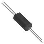
| 描述 | OPTOISOLATOR 10KV TRANS AXIAL晶体管输出光电耦合器 Output Photosensor Input Diode |
| 产品分类 | |
| 品牌 | TT Electronics/Optek Technology |
| 产品手册 | |
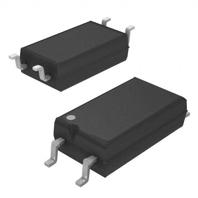
| 产品图片 |
|
| rohs | 符合RoHS无铅 / 符合限制有害物质指令(RoHS)规范要求 |
| 产品系列 | 光耦合器/光电耦合器,晶体管输出光电耦合器,Optek / TT Electronics OPI1264B- |
| 数据手册 | |
| 产品型号 | OPI1264B |
| Vce饱和值(最大值) | 400mV |
| 上升/下降时间(典型值) | - |
| 产品培训模块 | http://www.digikey.cn/PTM/IndividualPTM.page?site=cn&lang=zhs&ptm=6071 |
| 产品目录页面 | |
| 产品种类 | 晶体管输出光电耦合器 |
| 供应商器件封装 | 轴向 |
| 其它名称 | 365-1032 |
| 包装 | 散装 |
| 商标 | Optek / TT Electronics |
| 安装类型 | 通孔 |
| 封装 | Bulk |
| 封装/外壳 | 径向 - 4 引线 |
| 工作温度 | -40°C ~ 85°C |
| 工厂包装数量 | 25 |
| 打开/关闭时间(典型值) | - |
| 最大功率耗散 | 100 mW |
| 最大反向二极管电压 | 2 V |
| 最大工作温度 | + 85 C |
| 最大正向二极管电压 | 1.6 V |
| 最大输入二极管电流 | 40 mA |
| 最大集电极/发射极电压 | 30 V |
| 最大集电极/发射极饱和电压 | 0.4 V |
| 最小工作温度 | - 40 C |
| 标准包装 | 25 |
| 正向电流 | 10 mA |
| 每芯片的通道数量 | 1 Channel |
| 电压-正向(Vf)(典型值) | 1.6V (最小值) |
| 电压-输出(最大值) | 30V |
| 电压-隔离 | 10000VDC |
| 电流-DC正向(If) | 40mA |
| 电流-输出/通道 | 44mA |
| 电流传输比(最大值) | 125% @ 10mA |
| 电流传输比(最小值) | 50% @ 10mA |
| 电流传递比 | 50 % |
| 绝缘电压 | 10000 Vrms |
| 输入类型 | DC |
| 输出类型 | 晶体管 |
| 输出设备 | NPN Phototransistor |
| 通道数 | 1 |


.jpg)
(B)(TU)-VG.jpg)


- 商务部:美国ITC正式对集成电路等产品启动337调查
- 曝三星4nm工艺存在良率问题 高通将骁龙8 Gen1或转产台积电
- 太阳诱电将投资9.5亿元在常州建新厂生产MLCC 预计2023年完工
- 英特尔发布欧洲新工厂建设计划 深化IDM 2.0 战略
- 台积电先进制程称霸业界 有大客户加持明年业绩稳了
- 达到5530亿美元!SIA预计今年全球半导体销售额将创下新高
- 英特尔拟将自动驾驶子公司Mobileye上市 估值或超500亿美元
- 三星加码芯片和SET,合并消费电子和移动部门,撤换高东真等 CEO
- 三星电子宣布重大人事变动 还合并消费电子和移动部门
- 海关总署:前11个月进口集成电路产品价值2.52万亿元 增长14.8%
.jpg)

.jpg)

PDF Datasheet 数据手册内容提取
Optically Coupled Isolator OPI110, OPI1264 Series Features: 15 kV electrical isolation Choice of phototransistor Low-cost plastic housing UL recognized File No. E58730 Description: Each Optoisolator in this data sheet contains an infrared Light Emitting Diode (LED) and a NPN silicon Photosensor. The OPI110 and OPI1264 devices have 890 nm Light Emitting Diode (LED) and NPN phototransistor sensor. The devices are sealed in a precast opaque housing with a optically transmissive path between the LED and the photosensor. The Optoisolators in this data sheet are UL recognised under E58730. This series is designed for transmission of information between one power supply voltage and another where the potentials during surge conditions are not greater than the guaranteed isolation voltage. Custom electrical, wire and cabling and connectors are available. Contact your local representative or OPTEK for more information. Applications: High voltage isolation between input and output Electrical isolation in dirty environments Industrial equipment Medical equipment Ordering Information LED Isolation CTR V Lead Part I (mA) CE Peak Sensor Voltage Min / F (Volts) Length / Number Typ / Max Wavelength (,000) Max Max Spacing OPI110 12.5 / NA OPI110A 25 / NA Transistor 10 / 40 OPI110B 50 / 125 OPI110C 100 / NA 890 nm 15 30 0 . 5 0 " / 0.55" OPI1264 12.5 / NA OPI1264A 25 / NA Transistor 10 / 40 OPI1264B 50 / 125 OPI1264C 100 / NA General Note TT Electronics | OPTEK Technology TT Electronics reserves the right to make changes in product specification without 1645 Wallace Drive, Carrollton, TX 75006|Ph: +1 972 323 2200 notice or liability. All information is subject to TT Electronics’ own data and is www.ttelectronics.com | sensors@ttelectronics.com considered accurate at time of going to print. © TT electronics plc Issue C 11/2017 Page 1
Optically Coupled Isolator OPI110, OPI1264 Series Absolute Maximum Ratings (T = 25o C unless otherwise noted) A Storage Temperature -40° C to +100° C Operating Temperature -40° C to +85° C Input-to-Output Isolation Voltage(1)(2) ± 15 kVDC Lead Soldering Temperature (1/16” (1.6 mm) from case for 5 seconds with soldering iron)(3) 260° C Input Diode Forward DC Current 40 mA Reverse DC Voltage 2 V Power Dissipation(4) 50 mW Output Photosensor Collector-Emitter Voltage 30 OPI110, OPI1264 Emitter-Collector Voltage 5 Power Dissipation(5) 100 mW Notes: (1) Measured with input and output leads shorted. Typical input/output capacitance is 0.06 pF. (2) UL recognition is for 15kV dc for one minute. (3) RMA flux is recommended. The duration can be extended to 10 seconds maximum when flow soldering. (4) Derate linearly 0.83 mW/°C above 25°C. (5) Derate linearly 1.67 mW/°C above 25°C. OPI110 OPI1264 1 4 1 4 2 3 2 3 General Note TT Electronics | OPTEK Technology TT Electronics reserves the right to make changes in product specification without 1645 Wallace Drive, Carrollton, TX 75006|Ph: +1 972 323 2200 notice or liability. All information is subject to TT Electronics’ own data and is www.ttelectronics.com | sensors@ttelectronics.com considered accurate at time of going to print. © TT electronics plc Issue C 11/2017 Page 2
Optically Coupled Isolator OPI110, OPI1264 Series Electrical Characteristics (T = 25o C unless otherwise noted) A SYMBOL PARAMETER MIN TYP MAX UNITS TEST CONDITIONS Input Diode (See OP265 for additional information - for reference only) V Forward Voltage - - 1.6 V I = 20 mA F F I Reverse Current - - 100 µA V = 2 V R R Output Photosensor (See OP505 for additional information - for reference only) Collector-Emitter Breakdown Voltage V (BR)CEO OPI110, OPI1264 30 - - V I = 100 µA C Emitter-Collector Breakdown Voltage V OPI110 5 - - V I = 100 µA, I = 0 (BR)ECO E F OPI1264 - - - I = 100 µA E Collector-Emitter Dark Current I nA CEO OPI110, OPI1264 - - 100 V = 15 V, E = 0 CE E Coupled Coupled “ON” Current I 1.25 - 44 mA I = 10mA V = 5V C(ON) OPI110, OPI1264 F CE DC Current Transfer Ratio OPI110, OPI1264 12.5 - - I = 10 mA, V = 5 V F CE I I OPI110A, OPI1264A 25.0 - - % I = 10 mA, V = 5 V C/F F CE OPI110B, OPI1264B 50.0 - 125 I = 10 mA, V = 5 V F CE OPI110C, OPI1264C 100.0 - - I = 10 mA, V = 5 V F CE Collector Saturation Voltage V V CE(SAT) OPI110, OPI1264 - - 0.4 I = 10 mA, I = 1.6 mA F C Collector-Emitter Dark Current I nA CEO OPI110, OPI1264 - - 200 V = 20 V, I = 0 CE F V Isolation Voltage 15 - - kVDC See Note 1. ISO Notes: (1) Measured with input and output leads shorted. Typical input/output capacitance is 0.06 pF. General Note TT Electronics | OPTEK Technology TT Electronics reserves the right to make changes in product specification without 1645 Wallace Drive, Carrollton, TX 75006|Ph: +1 972 323 2200 notice or liability. All information is subject to TT Electronics’ own data and is www.ttelectronics.com | sensors@ttelectronics.com considered accurate at time of going to print. © TT electronics plc Issue C 11/2017 Page 3
Mouser Electronics Authorized Distributor Click to View Pricing, Inventory, Delivery & Lifecycle Information: T T Electronics: OPI1264A OPI1264B OPI110C OPI110 OPI110A OPI110B OPI1264 OPI1264C