ICGOO在线商城 > 传感器,变送器 > 光学传感器 - 光断续器 - 槽型 - 晶体管输出 > OPB840W11Z
 Datasheet下载
- 型号: OPB840W11Z
- 制造商: OPTEK
- 库位|库存: xxxx|xxxx
- 要求:
| 数量阶梯 | 香港交货 | 国内含税 |
| +xxxx | $xxxx | ¥xxxx |
查看当月历史价格
查看今年历史价格
OPB840W11Z产品简介:
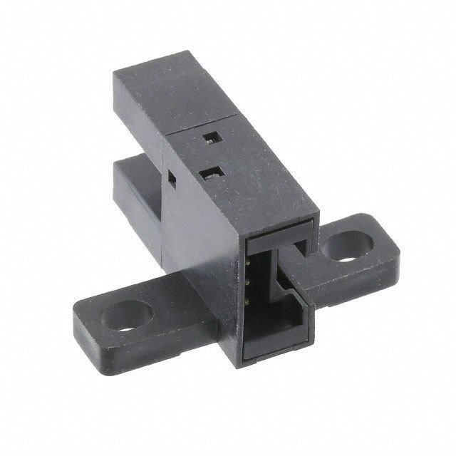
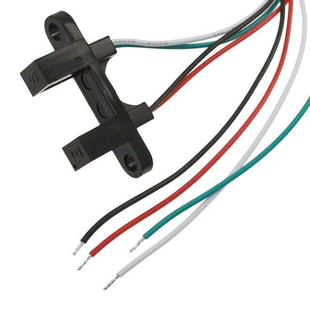
ICGOO电子元器件商城为您提供OPB840W11Z由OPTEK设计生产,在icgoo商城现货销售,并且可以通过原厂、代理商等渠道进行代购。 OPB840W11Z价格参考。OPTEKOPB840W11Z封装/规格:光学传感器 - 光断续器 - 槽型 - 晶体管输出, Optical Sensor Transmissive 0.125" (3.18mm) Phototransistor Module, Pre-Wired。您可以下载OPB840W11Z参考资料、Datasheet数据手册功能说明书,资料中有OPB840W11Z 详细功能的应用电路图电压和使用方法及教程。
TT Electronics/Optek Technology的OPB840W11Z是一款光学传感器,具体属于光断续器(也称作光电开关或槽型光电传感器),采用晶体管输出设计。这种类型的传感器广泛应用于各种自动化和工业控制领域,其主要功能是通过检测物体的通过或位置变化来触发信号输出。

 应用场景:

1. 自动化生产线:
   - 在自动化生产线中,OPB840W11Z可以用于检测传送带上的物品是否到达特定位置。例如,在包装线上,它可以检测到每个包装盒的位置,确保它们按顺序进行下一步操作。

2. 计数与测量:
   - 该传感器可以用于计数通过的物体数量。例如,在物流分拣系统中,它可以精确地统计经过的包裹数量,帮助提高工作效率和准确性。

3. 限位与定位:
   - 在机械设备中,OPB840W11Z可以用作限位开关,检测机械臂或其他运动部件是否到达预定位置。这有助于防止设备超程或发生碰撞,确保安全运行。

4. 编码器反馈:
   - 在电机控制系统中,该传感器可以作为编码器的一部分,提供旋转角度或线性位移的反馈信号,从而实现精确的速度和位置控制。

5. 纸张、标签检测:
   - 在印刷、包装等行业中,OPB840W11Z可以用于检测纸张或标签的存在与否,确保在正确的时间进行裁切或粘贴操作。

6. 电梯门检测:
   - 在电梯系统中,该传感器可以安装在电梯门的边缘,检测是否有物体或人阻碍门的关闭,从而防止夹伤事故的发生。

7. 自动门控制:
   - 在商场、办公楼等场所的自动门系统中,OPB840W11Z可以用于检测是否有行人接近,从而自动打开或关闭门,提升通行效率和安全性。

8. 液位检测:
   - 在一些液体容器中,OPB840W11Z可以用于检测液位高度,确保容器内的液体不会溢出或过低,适用于化工、制药等行业。

总之,OPB840W11Z凭借其高精度、可靠性和广泛应用范围,成为许多自动化和工业应用中的理想选择。
| 参数 | 数值 |
| 产品目录 | |
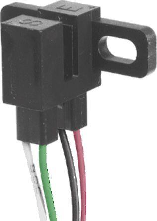
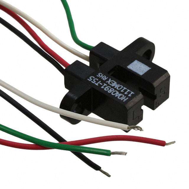
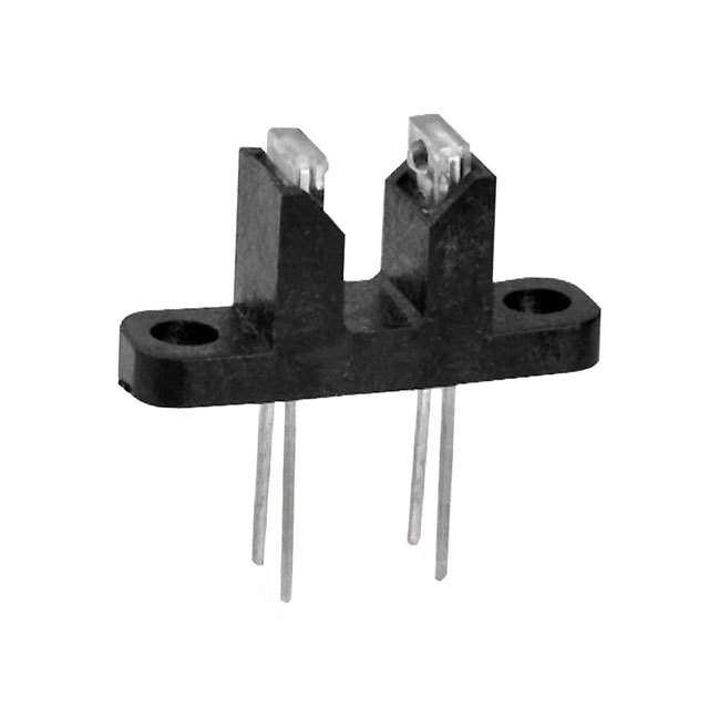
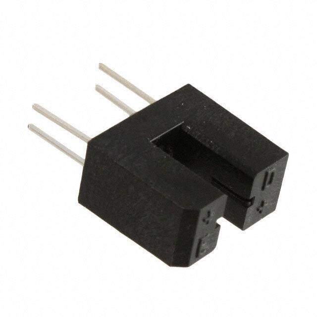
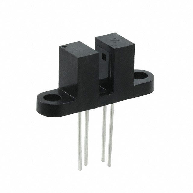
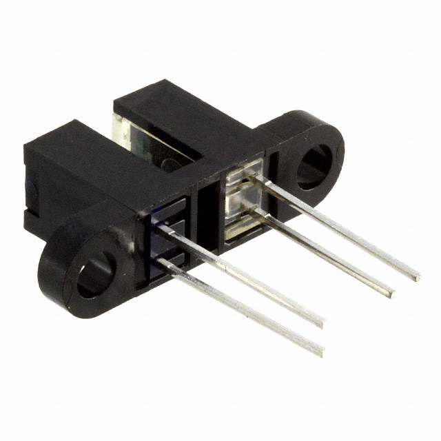
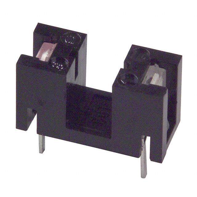
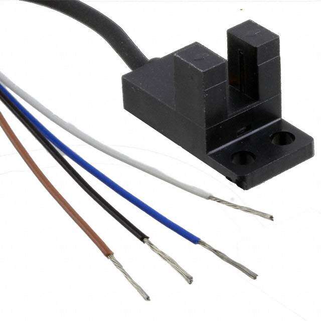
| 描述 | SENS OPTO SLOT 3.18MM TRANS C-MT光学开关(透射型,光电晶体管输出) Output Phototranstr Input Diode |
| 产品分类 | |
| 品牌 | Optek / TT Electronics |
| 产品手册 | |
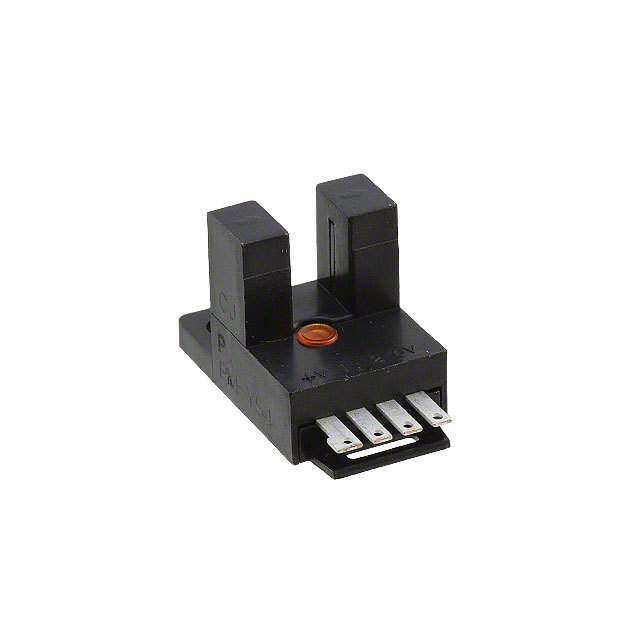
| 产品图片 |
|
| rohs | 符合RoHS无铅 / 符合限制有害物质指令(RoHS)规范要求 |
| 产品系列 | 光学开关(透射型,光电晶体管输出),Optek / TT Electronics OPB840W11Z- |
| 数据手册 | |
| 产品型号 | OPB840W11Z |
| 产品培训模块 | http://www.digikey.cn/PTM/IndividualPTM.page?site=cn&lang=zhs&ptm=6246 |
| 产品目录页面 | |
| 产品种类 | 光学开关(透射型,光电晶体管输出) |
| 光圈宽度 | 0.254 mm |
| 其它名称 | 365-1337 |
| 功率耗散 | 100 mW |
| 包装 | 散装 |
| 响应时间 | - |
| 商标 | Optek / TT Electronics |
| 安装类型 | 底座安装 |
| 封装 | Bulk |
| 封装/外壳 | 模块,预接线 |
| 工作温度 | -40°C ~ 80°C |
| 工厂包装数量 | 25 |
| 感应方式 | Transmissive, Slotted |
| 感应方法 | 可传导的 |
| 感应距离 | 0.125" (3.18mm) |
| 最大工作温度 | + 80 C |
| 最大集电极电流 | 30 mA |
| 最小工作温度 | - 40 C |
| 标准包装 | 25 |
| 槽宽 | 3.18 mm |
| 正向电流 | 50 mA |
| 波长 | 880 nm |
| 电压-集射极击穿(最大值) | 30V |
| 电流-DC正向(If) | 50mA |
| 电流-集电极(Ic)(最大值) | 30mA |
| 类型 | 无放大 |
| 输出设备 | Phototransistor |
| 输出配置 | 光电晶体管 |
| 集电极—发射极最大电压VCEO | 30 V |


- 商务部:美国ITC正式对集成电路等产品启动337调查
- 曝三星4nm工艺存在良率问题 高通将骁龙8 Gen1或转产台积电
- 太阳诱电将投资9.5亿元在常州建新厂生产MLCC 预计2023年完工
- 英特尔发布欧洲新工厂建设计划 深化IDM 2.0 战略
- 台积电先进制程称霸业界 有大客户加持明年业绩稳了
- 达到5530亿美元!SIA预计今年全球半导体销售额将创下新高
- 英特尔拟将自动驾驶子公司Mobileye上市 估值或超500亿美元
- 三星加码芯片和SET,合并消费电子和移动部门,撤换高东真等 CEO
- 三星电子宣布重大人事变动 还合并消费电子和移动部门
- 海关总署:前11个月进口集成电路产品价值2.52万亿元 增长14.8%
PDF Datasheet 数据手册内容提取
Slotted Optical Switch OPB830 and OPB840 (L and W) Features: 0.125” (3.18 mm) wide slot L Package Choice of electrical output parameters Choice of aperture Choice of opaque or IR transmissive shell material Side mount configuration Choice of lead spacing (L Series) W Package 24” [610 mm] 26 AWG wire leads (W Series) Description: OPB830 and OPB840 series provide the design engineer with the flexibility of a custom device from a standard product line. The L Series offers a choice of PCBoard mount lead spacing, while the W Series offers 24” (610mm) 26AWG wire leads. Building from a standard housing that utilizes a .375” (9.5 mm) wide slot, a user can specify the electrical output parameters, choice of aperture, discrete shell material, side mount configuration, and a choice of lead spacing (for the L Series) or 24” [610 mm] UL approved 26 AWG wire leads (W Series). Housings are made from an opaque grade of injection-molded plastic that minimizes the assembly’s sensitivity to visible and near-infrared ambient radiation. Discrete shells (exposed on the parallel faces inside the device throat) are made of either IR transmissive plastic (for applications where aperture contamination may occur) or of opaque plastic with aperture openings (for maximum protection against ambient light). Switching of the phototransistor occurs whenever an opaque object passes through the slot and interrupts the beam. Applications: Non-contact interruptive object sensing Assembly line automation Machine automation Equipment security Machine safety General Note TT Electronics | Optek Technology, Inc. TT Electronics reserves the right to make changes in product specification without 1645 Wallace Drive, Ste. 130, Carrollton, TX USA 75006 |Ph: +1 972 323 2200 notice or liability. All information is subject to TT Electronics’ own data and is www.ttelectronics.com | sensors@ttelectronics.com considered accurate at time of going to print. © TT electronics plc Issue A 11/2016 Page 1
Slotted Optical Switch OPB830 and OPB840 (L and W) Electrical Specifications Absolute Maximum Ratings (T =25°C unless otherwise noted) A Storage and Operating Temperature L Series(1) -40° C to +85°C W Series(1) -40° C to +80°C Lead Soldering Temperature [1/16 inch (1.6mm) from the case for 5 sec. with soldering iron](2) 260°C Input Diode Forward DC Current 50 mA Peak Forward Current (1 µs pulse width, 300 pps) 1 A Reverse DC Voltage 2 V Power Dissipation(1) 100 mW Output Phototransistor Collector-Emitter Voltage 30 V Emitter-Collector Voltage 5 V Collector DC Current 30 mA Power Dissipation(1) 100 mW Electrical Characteristics (T = 25°C unless otherwise noted) A SYMBOL PARAMETER MIN TYP MAX UNITS TEST CONDITIONS Input Diode LED (See OP240 for additional information—for reference only) V Forward Voltage - - 1.7 V I = 20 mA F F I Reverse Current - - 100 µA V = 2 V R R Output Transistor (See OP550 for additional information—for reference only) V Collector-Emitter Breakdown Voltage 30 - - V I = 1 mA (BR)CEO C V Emitter-Collector Breakdown Voltage 5 - - V I = 100 µA (BR)ECO E I Collector-Emitter Dark Current - - 100 nA V = 10 V CEO CE Notes: (1) Derate linearly 1.67 mW/° C above 25° C for L Series. (2) RMA flux is recommended. Duration can be extended to 10 seconds maximum when flow soldering. (3) Methanol or isopropanol are recommended as cleaning agents. Plastic housing is soluble in chlorinated hydrocarbons and ketones. (4) The W Series includes wire terminations of 24” (610 mm) 7-strand, 26 AWG UL insulated wire on each terminal. Each device incorporates a wire strain relief at the housing surface. The insulation functions and colors are: anode (red), cathode (black), phototransistor collector (white) and phototransistor emitter (green). (5) All parameters tested using pulse technique. General Note TT Electronics | Optek Technology, Inc. TT Electronics reserves the right to make changes in product specification without 1645 Wallace Drive, Ste. 130, Carrollton, TX USA 75006 |Ph: +1 972 323 2200 notice or liability. All information is subject to TT Electronics’ own data and is www.ttelectronics.com | sensors@ttelectronics.com considered accurate at time of going to print. © TT electronics plc Issue A 11/2016 Page 2
Slotted Optical Switch OPB830 and OPB840 (L and W) Electrical Characteristics (T = 25°C unless otherwise noted) A SYMBOL PARAMETER MIN TYP MAX UNITS TEST CONDITIONS Combined Collector-Emitter Saturation Voltage Parameter A (OPB830L,OPB840L) (OPB835L, OPB845L) - - 0.4 V I = 400 µA, I = 20 mA (OPB830W,OPB840W) C F (OPB835W, OPB845W) Parameter B (OPB831L,OPB841L) V (OPB836L,OPB846L) CE(SAT) - - 0.4 V I = 800 µA, I = 10 mA (OPB831W,OPB841W) C F (OPB836W,OPB846W) Parameter C (OPB832L,OPB842L) (OPB837L,OPB847L) - - 0.6 V I = 1800 µA, I = 20 mA (OPB832W,OPB842W) C F (OPB837W,OPB847W) On-State Collector Current Parameter A (OPB830L,OPB840L) (OPB835L, OPB845L) - - 0.625 mA V = 10 V, I = 20 mA (OPB830W,OPB840W) CE F (OPB835W, OPB845W) Parameter B (OPB831L,OPB841L) I (OPB836L,OPB846L) C(ON) 1.250 - - mA V = 5 V, I = 10 mA (OPB831W,OPB841W) CE F (OPB836W,OPB846W) Parameter C (OPB832L,OPB842L) (OPB837L,OPB847L) mA 2.250 - - V = .6 V, I = 20 mA (OPB832W,OPB842W) CE F (OPB837W,OPB847W) General Note TT Electronics | Optek Technology, Inc. TT Electronics reserves the right to make changes in product specification without 1645 Wallace Drive, Ste. 130, Carrollton, TX USA 75006 |Ph: +1 972 323 2200 notice or liability. All information is subject to TT Electronics’ own data and is www.ttelectronics.com | sensors@ttelectronics.com considered accurate at time of going to print. © TT electronics plc Issue A 11/2016 Page 3
Slotted Optical Switch OPB830 and OPB840 (L and W) OPOBP8B_3 _70 LT1111 -- FFllaagg NNeexxt tt oto E Emmittiettrer OPOBP8B_3 _7 0LT1111 -- FFllaagg NNeexxtt t too S Seennsosror 1.20 1.20 Top to Bottom Top to Bottom 1.00 1.00 A) A) m0.80 m0.80 se ( Left to Right Right to Left se ( Left to Right Right to Left n n o o p p s s Re0.60 Re0.60 N) N) O O C( C( al I al I c c pi0.40 pi0.40 y y T T 0.20 0.20 0.00 0.00 0.00 0.05 0.10 0.15 0.20 0.25 0.00 0.05 0.10 0.15 0.20 0.25 Displacement Distance (inches) Displacement Distance (inches) OPOBPB83_7 _0 TL1111 - -F Flalga gin i nM iMddidled olef Solfo Stlot 1.20 Top to Bottom 1.00 Top to Bottom 0 A) m 0.80 se ( Left to Right Right to Left n o p s Re 0.60 N) Emitter O C( al I Left to Right Right to Left c pi 0.40 y T Sensor 0.20 0 Width 0.00 0.00 0.05 0.10 0.15 0.20 0.25 Diisplacement Distance (inches) General Note TT Electronics | Optek Technology, Inc. TT Electronics reserves the right to make changes in product specification without 1645 Wallace Drive, Ste. 130, Carrollton, TX USA 75006 |Ph: +1 972 323 2200 notice or liability. All information is subject to TT Electronics’ own data and is www.ttelectronics.com | sensors@ttelectronics.com considered accurate at time of going to print. © TT electronics plc Issue A 11/2016 Page 4
Slotted Optical Switch OPB830 and OPB840 (L and W) OPOBP8B_3 7_0 LN5511 -- FFllaagg i nN eMxidt dtole E omf Sitltoetr OPOBP8B_3 _7 0LN5511 - - FFllaagg NNeexxtt ttoo SSeennssoorr 1.20 1.20 Top to Bottom Top to Bottom 1.00 1.00 A) A) m 0.80 m 0.80 se ( se ( Left to Right Right to Left n Left to Right Right to Left n o o p p s s Re 0.60 Re 0.60 N) N) O O C( C( al I al I c c pi 0.40 pi 0.40 y y T T 0.20 0.20 0.00 0.00 0.00 0.05 0.10 0.15 0.20 0.25 0.00 0.05 0.10 0.15 0.20 0.25 Displacement Distance (inches) Displacement Distance (inches) OOPPBB83_7 _0 NL5511 - - F Flalagg i nin M Mididdlde loef oSfl oStlot 1.20 Top to Bottom 1.00 Top to Bottom 0 A) m 0.80 e ( s n Left to Right Right to Left o p s e 0.60 R Emitter N) O C( Left to Right Right to Left al I c pi 0.40 y T Sensor 0 Width 0.20 0.00 0.00 0.05 0.10 0.15 0.20 0.25 Displacement Distance (inches) General Note TT Electronics | Optek Technology, Inc. TT Electronics reserves the right to make changes in product specification without 1645 Wallace Drive, Ste. 130, Carrollton, TX USA 75006 |Ph: +1 972 323 2200 notice or liability. All information is subject to TT Electronics’ own data and is www.ttelectronics.com | sensors@ttelectronics.com considered accurate at time of going to print. © TT electronics plc Issue A 11/2016 Page 5
Slotted Optical Switch OPB830 and OPB840 (L and W) OPBO8P_B 3_8 L0T5555 - - FFllaagg NNeexxtt t oto E Emmittiettrer OPBO8P_B 3_8 L0T5555 - -F Fllaagg NNeexxtt ttoo S Seennsosror 1.20 1.20 Top to Bottom Top to Bottom 1.00 1.00 A) A) m 0.80 m 0.80 e ( e ( s s pon Left to Right Right to Left pon Left to Right Right to Left s s Re 0.60 Re 0.60 al I C(ON) al I C(ON) c c pi 0.40 pi 0.40 y y T T 0.20 0.20 0.00 0.00 0.00 0.05 0.10 0.15 0.20 0.25 0.00 0.05 0.10 0.15 0.20 0.25 Displacement Distance (inches) Displacement Distance (inches) OPOBP8B_3 8_0 TL5555 -- F Flalagg in i nM Mididdled loef oSflo Stlot 1.20 Top to Bottom 1.00 Top to Bottom 0 A) m e ( 0.80 s n po Left to Right Right to Left s Re 0.60 N) Emitter O al IC( Left to Right Right to Left pic 0.40 y T Sensor 0 Width 0.20 0.00 0.00 0.05 0.10 0.15 0.20 0.25 Displacement Distance (inches) General Note TT Electronics | Optek Technology, Inc. TT Electronics reserves the right to make changes in product specification without 1645 Wallace Drive, Ste. 130, Carrollton, TX USA 75006 |Ph: +1 972 323 2200 notice or liability. All information is subject to TT Electronics’ own data and is www.ttelectronics.com | sensors@ttelectronics.com considered accurate at time of going to print. © TT electronics plc Issue A 11/2016 Page 6
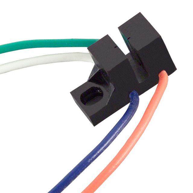
Slotted Optical Switch OPB830 and OPB840 (L and W) Packaging OPB830/840L Series 1 3 2 4 Pin # / Color Description 1 / Black Cathode 2 / Red Anode OPB830/840W Series 3 / White Collector 4 / Green Emitter DIMENSIONS ARE IN: [ MILLIMETERS] INCHES General Note TT Electronics | Optek Technology, Inc. TT Electronics reserves the right to make changes in product specification without 1645 Wallace Drive, Ste. 130, Carrollton, TX USA 75006 |Ph: +1 972 323 2200 notice or liability. All information is subject to TT Electronics’ own data and is www.ttelectronics.com | sensors@ttelectronics.com considered accurate at time of going to print. © TT electronics plc Issue A 11/2016 Page 7
Slotted Optical Switch OPB830 and OPB840 (L and W) Part Number Guide — OPB8XX OPB 8 X X L X X Optek Assembly Sensor Aperture: 1 — 0.010” (0.25 mm) 5 — 0.050” (1.27 mm) Phototransistor Output Family Emitter Aperture: 1 — 0.010” (0.25 mm) 5 — 0.050” (1.27 mm) Discrete Shell Material: Mounting configurations: 3 — Side mount IR transmissive L — Solder lead termination Plastic discrete shell 4 — Side mount opaque Electrical Specification Variations: Plastic discrete shell 0 = Electrical Parameter A - (0.320” lead spacing) 1 = Electrical Parameter B - (0.320” lead spacing) 2 = Electrical Parameter C - (0.320” lead spacing) 5 = Electrical Parameter A - (0.220” lead spacing) 6 = Electrical Parameter B - (0.220” lead spacing) 7 = Electrical Parameter C - (0.220” lead spacing) Notes: Assemblies with dual 0.010” apertures are currently available with electrical parameter “A” only. Part Number Guide — OPB8XX OPB 8 X X W X X Z Optek Assembly Sensor Aperture: 1 — 0.010” (0.25 mm) 5 — 0.050” (1.27 mm) Phototransistor Output Family Emitter Aperture: 1 — 0.010” (0.25 mm) 5 — 0.050” (1.27 mm) Discrete Shell Material: Mounting configurations: 3 — Side mount IR transmissive W — Wire termination Plastic discrete shell • Parts ending with “Z” meet 4 — Side mount opaque Electrical Specification Variations: RoHS requirements Plastic discrete shell 0 = Electrical Parameter A • Wires = 26 AWG—24” Long 1 = Electrical Parameter B 2 = Electrical Parameter C Notes: Assemblies with dual 0.010” apertures are currently available with electrical parameter “A” only. General Note TT Electronics | Optek Technology, Inc. TT Electronics reserves the right to make changes in product specification without 1645 Wallace Drive, Ste. 130, Carrollton, TX USA 75006 |Ph: +1 972 323 2200 notice or liability. All information is subject to TT Electronics’ own data and is www.ttelectronics.com | sensors@ttelectronics.com considered accurate at time of going to print. © TT electronics plc Issue A 11/2016 Page 8