ICGOO在线商城 > 集成电路(IC) > 线性 - 放大器 - 仪表,运算放大器,缓冲器放大器 > OPA552FAKTWT
 Datasheet下载
- 型号: OPA552FAKTWT
- 制造商: Texas Instruments
- 库位|库存: xxxx|xxxx
- 要求:
| 数量阶梯 | 香港交货 | 国内含税 |
| +xxxx | $xxxx | ¥xxxx |
查看当月历史价格
查看今年历史价格
OPA552FAKTWT产品简介:
ICGOO电子元器件商城为您提供OPA552FAKTWT由Texas Instruments设计生产,在icgoo商城现货销售,并且可以通过原厂、代理商等渠道进行代购。 OPA552FAKTWT价格参考¥25.45-¥47.28。Texas InstrumentsOPA552FAKTWT封装/规格:线性 - 放大器 - 仪表,运算放大器,缓冲器放大器, 通用 放大器 1 电路 DDPAK/TO-263-7。您可以下载OPA552FAKTWT参考资料、Datasheet数据手册功能说明书,资料中有OPA552FAKTWT 详细功能的应用电路图电压和使用方法及教程。
| 参数 | 数值 |
| -3db带宽 | - |
| 产品目录 | 集成电路 (IC)半导体 |
| 描述 | IC OPAMP GP 12MHZ DDPAK运算放大器 - 运放 High-Volt High-Crnt Oper Amplifier |
| 产品分类 | Linear - Amplifiers - Instrumentation, OP Amps, Buffer Amps集成电路 - IC |
| 品牌 | Texas Instruments |
| 产品手册 | |
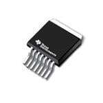
| 产品图片 |
|
| rohs | 符合RoHS无铅 / 符合限制有害物质指令(RoHS)规范要求 |
| 产品系列 | 放大器 IC,运算放大器 - 运放,Texas Instruments OPA552FAKTWT- |
| 数据手册 | |
| 产品型号 | OPA552FAKTWT |
| 产品种类 | 运算放大器 - 运放 |
| 供应商器件封装 | DDPAK/TO-263-7 |
| 共模抑制比—最小值 | 92 dB |
| 关闭 | Shutdown |
| 其它名称 | 296-15970-1 |
| 包装 | 剪切带 (CT) |
| 压摆率 | 24 V/µs |
| 商标 | Texas Instruments |
| 增益带宽生成 | 12 MHz |
| 增益带宽积 | 12MHz |
| 安装类型 | 表面贴装 |
| 安装风格 | SMD/SMT |
| 封装 | Reel |
| 封装/外壳 | TO-263-8,D²Pak(7 引线+接片),TO-263CA |
| 封装/箱体 | TO-263-7 |
| 工作温度 | -40°C ~ 125°C |
| 工作电源电压 | +/- 4 V to +/- 30 V |
| 工厂包装数量 | 50 |
| 放大器类型 | 通用 |
| 最大双重电源电压 | +/- 30 V |
| 最大工作温度 | + 125 C |
| 最小双重电源电压 | +/- 4 V |
| 最小工作温度 | - 40 C |
| 标准包装 | 1 |
| 电压-电源,单/双 (±) | 8 V ~ 60 V, ±4 V ~ 30 V |
| 电压-输入失调 | 1mV |
| 电流-电源 | 7mA |
| 电流-输入偏置 | 20pA |
| 电流-输出/通道 | 200mA |
| 电源电流 | 8.5 mA |
| 电路数 | 1 |
| 系列 | OPA552 |
| 设计资源 | http://www.digikey.com/product-highlights/cn/zh/texas-instruments-webench-design-center/3176 |
| 转换速度 | 24 V/us |
| 输入偏压电流—最大 | 100 pA |
| 输入参考电压噪声 | 14 nV |
| 输入补偿电压 | 3 mV |
| 输出电流 | 200 mA |
| 输出类型 | - |
| 通道数量 | 1 Channel |


- 商务部:美国ITC正式对集成电路等产品启动337调查
- 曝三星4nm工艺存在良率问题 高通将骁龙8 Gen1或转产台积电
- 太阳诱电将投资9.5亿元在常州建新厂生产MLCC 预计2023年完工
- 英特尔发布欧洲新工厂建设计划 深化IDM 2.0 战略
- 台积电先进制程称霸业界 有大客户加持明年业绩稳了
- 达到5530亿美元!SIA预计今年全球半导体销售额将创下新高
- 英特尔拟将自动驾驶子公司Mobileye上市 估值或超500亿美元
- 三星加码芯片和SET,合并消费电子和移动部门,撤换高东真等 CEO
- 三星电子宣布重大人事变动 还合并消费电子和移动部门
- 海关总署:前11个月进口集成电路产品价值2.52万亿元 增长14.8%


PDF Datasheet 数据手册内容提取
Product Sample & Technical Tools & Support & Folder Buy Documents Software Community OPA551,OPA552 SBOS100B–JULY1999–REVISEDJANUARY2016 OPA55x High-Voltage, High-Current Operational Amplifiers 1 Features 3 Description • WideSupplyRange:±4Vto ±30V The OPA551x devices are low-cost operational 1 amplifiers with high-voltage (60-V) and high-current • HighOutputCurrent:200mAContinuous (200-mA)capability. • LowNoise:14nV/√Hz The OPA551 is unity-gain stable and features high • FullyProtected: slew rate (15 V/µs) and wide bandwidth (3 MHz). The – ThermalShutdown OPA552 is optimized for gains of 5 or greater, and – OutputCurrent-Limited offers higher speed with a slew rate of 24 V/µs and a bandwidth of 12 MHz. Both devices are suitable for • ThermalShutdownIndicator telephony,audio,servo,andtestapplications. • WideOutputSwing:2VfromRail These laser-trimmed, monolithic integrated circuits • FastSlewRate: provide excellent low-level accuracy along with high – OPA551:15V/µs output swing. High performance is maintained as the – OPA552:24V/µs amplifierswingstoitsspecifiedlimits. • WideBandwidth: The OPA55x devices are internally protected against – OPA551:3MHz overtemperature conditions and current overloads. The thermal shutdown indicator flag provides a – OPA552:12MHz current output to alert the user when thermal • Packages:PDIP-8,SOIC-8,orDDPAK/TO-263-7 shutdownhasoccurred. The OPA55x devices are available in PDIP-8 and 2 Applications SOIC-8 packages, as well as a DDPAK-7/TO-263 • Telephony surface-mount plastic power package. They are • TestEquipment specified for operation over the extended industrial temperaturerange,–40°Cto+125°C. • AudioAmplifiers • TransducerExcitation DeviceInformation(1) • ServoDrivers PARTNUMBER PACKAGE BODYSIZE(NOM) PDIP(8) 9.81mm×6.35mm OPA55x SOIC(8) 4.9mm×3.91mm DDPAK/TO-263(7) 10.1mm×8.99mm (1) For all available packages, see the orderable addendum at theendofthedatasheet. SimplifiedFunctionalDiagram V+ V–IN – OPA551 VO V+IN + Flag V– 1 An IMPORTANT NOTICE at the end of this data sheet addresses availability, warranty, changes, use in safety-critical applications, intellectualpropertymattersandotherimportantdisclaimers.PRODUCTIONDATA.
OPA551,OPA552 SBOS100B–JULY1999–REVISEDJANUARY2016 www.ti.com Table of Contents 1 Features.................................................................. 1 8.1 ApplicationInformation............................................13 2 Applications........................................................... 1 8.2 TypicalApplication .................................................13 3 Description............................................................. 1 9 PowerSupplyRecommendations...................... 17 4 RevisionHistory..................................................... 2 9.1 PowerSupplies.......................................................17 5 PinConfigurationandFunctions......................... 3 10 Layout................................................................... 18 10.1 LayoutGuidelines.................................................18 6 Specifications......................................................... 4 10.2 LayoutExample....................................................18 6.1 AbsoluteMaximumRatings......................................4 10.3 PowerDissipation.................................................18 6.2 ESDRatings ............................................................4 10.4 SafeOperatingArea.............................................19 6.3 RecommendedOperatingConditions.......................4 10.5 HeatSinking.........................................................20 6.4 ThermalInformation..................................................4 11 DeviceandDocumentationSupport................. 21 6.5 ElectricalCharacteristics:V =±30V.......................5 S 6.6 TypicalCharacteristics..............................................7 11.1 DeviceSupport......................................................21 11.2 DocumentationSupport .......................................21 7 DetailedDescription............................................ 11 11.3 CommunityResources..........................................21 7.1 Overview.................................................................11 11.4 Trademarks...........................................................21 7.2 FunctionalBlockDiagram.......................................11 11.5 ElectrostaticDischargeCaution............................21 7.3 FeatureDescription.................................................11 11.6 Glossary................................................................21 7.4 DeviceFunctionalModes........................................12 12 Mechanical,Packaging,andOrderable 8 ApplicationandImplementation........................ 13 Information........................................................... 22 4 Revision History NOTE:Pagenumbersforpreviousrevisionsmaydifferfrompagenumbersinthecurrentversion. ChangesfromRevisionA(October2003)toRevisionB Page • AddedESDRatingtable,FeatureDescriptionsection,DeviceFunctionalModes,ApplicationandImplementation section,PowerSupplyRecommendationssection,Layoutsection,DeviceandDocumentationSupportsection,and Mechanical,Packaging,andOrderableInformationsection. ................................................................................................ 1 • Changedpackagereferencesthroughoutdocument:SO-8toSOIC-8andDDPAK-7toDDPAK-7/TO-263 .......................1 • DeletedleadtemperaturespecificationsfromAbsoluteMaximumRatingstable ................................................................. 4 • Deletedcharged-devicemodel(CDM)specificationfromESDRatingstable ...................................................................... 4 2 SubmitDocumentationFeedback Copyright©1999–2016,TexasInstrumentsIncorporated ProductFolderLinks:OPA551 OPA552
OPA551,OPA552 www.ti.com SBOS100B–JULY1999–REVISEDJANUARY2016 5 Pin Configuration and Functions OPA551,OPA552PPackage 8-PinPDIP OPA551,OPA552DPackage TopView 8-PinSOIC TopView NC 1 8 Flag V– 1 8 Flag –In 2 7 V+ –In 2 7 V+ +In 3 6 Out +In 3 6 Out V– 4 5 NC V– 4 5 V– OPA551,OPA552KTWPackage 7-PinDDPAK/TO-263Surface-Mount TopView 1 2 3 4 5 6 7 +In NC V+ Flag –In V– Out NOTE: TabisconnectedtoV–supply. PinFunctions PIN DDPAK/ I/O DESCRIPTION NAME SOIC PDIP TO-263 Flag 8 8 7 O Thermalshutdownindicator +IN 3 3 1 I Noninvertinginput –IN 2 2 2 I Invertinginput NC — 1,5 3 — Nointernalconnection(canbeleftfloating) Out 6 6 6 O Output Tab — — Tab — ConnecttoV–supply V+ 7 7 5 — Positive(highest)powersupply V– 1,4,5 4 4 — Negative(lowest)powersupply Copyright©1999–2016,TexasInstrumentsIncorporated SubmitDocumentationFeedback 3 ProductFolderLinks:OPA551 OPA552
OPA551,OPA552 SBOS100B–JULY1999–REVISEDJANUARY2016 www.ti.com 6 Specifications 6.1 Absolute Maximum Ratings(1) overoperatingfree-airtemperaturerange(unlessotherwisenoted) MIN MAX UNIT Supply,V =(V+)to(V–) 60 V S Inputvoltagerange,V (V–)–0.5 (V+)+0.5 V IN Output SeeSOACurve(SafeOperatingArea) Operatingtemperature,T –55 125 °C A Junctiontemperature,T 150 °C J Storagetemperature,T –65 150 °C stg (1) StressesbeyondthoselistedunderAbsoluteMaximumRatingsmaycausepermanentdamagetothedevice.Thesearestressratings only,whichdonotimplyfunctionaloperationofthedeviceattheseoranyotherconditionsbeyondthoseindicatedunderRecommended OperatingConditions.Exposuretoabsolute-maximum-ratedconditionsforextendedperiodsmayaffectdevicereliability. 6.2 ESD Ratings VALUE UNIT V Electrostaticdischarge Human-bodymodel(HBM),perANSI/ESDA/JEDECJS-001(1) ±3000 V (ESD) (1) JEDECdocumentJEP155statesthat500-VHBMallowssafemanufacturingwithastandardESDcontrolprocess. 6.3 Recommended Operating Conditions overoperatingfree-airtemperaturerange(unlessotherwisenoted) MIN MAX UNIT V Supplyvoltage 8(±4) 60(±30) V S Specifiedtemperature –40 125 °C 6.4 Thermal Information OPA551,OPA552 THERMALMETRIC(1) D P KTW UNIT (SOIC) (PDIP) (DDPAK/TO-263) 8PINS 8PINS 7PINS R Junction-to-ambientthermalresistance 96.7 44.1 22.7 °C/W θJA R Junction-to-case(top)thermalresistance 38.7 31.8 34.7 °C/W θJC(top) R Junction-to-boardthermalresistance 38.2 21.4 7.7 °C/W θJB ψ Junction-to-topcharacterizationparameter 3.7 9.1 3.3 °C/W JT ψ Junction-to-boardcharacterizationparameter 37.5 21.2 7.7 °C/W JB R Junction-to-case(bottom)thermalresistance — — 0.6 °C/W θJC(bot) (1) Formoreinformationabouttraditionalandnewthermalmetrics,seetheSemiconductorandICPackageThermalMetricsapplication report,SPRA953. 4 SubmitDocumentationFeedback Copyright©1999–2016,TexasInstrumentsIncorporated ProductFolderLinks:OPA551 OPA552
OPA551,OPA552 www.ti.com SBOS100B–JULY1999–REVISEDJANUARY2016 6.5 Electrical Characteristics: V = ±30 V S AtT =25°C(1),R =3kΩconnectedtoground,andV =0V,unlessotherwisenoted. J L OUT PARAMETER TESTCONDITIONS MIN TYP MAX UNIT OFFSETVOLTAGE VCM=0V,IO=0mA ±1 ±3 VOS Inputoffsetvoltage mV TJ=–40°Cto125°C ±5 dVOS/dT Inputoffsetvoltagevstemperature TJ=–40°Cto125°C ±7 µV/°C PSRR Inputoffsetvoltagevspowersupply VS=±4Vto±30V,VCM=0V 10 30 µV/V INPUTBIASCURRENT IB Inputbiascurrent ±20 ±100 pA IOS Inputoffsetcurrent ±3 ±100 pA NOISE en Inputvoltagenoisedensity f=1kHz 14 nV/√Hz in Currentnoisedensity f=1kHz 3.5 fA/√Hz INPUTVOLTAGERANGE VCM Common-modevoltagerange (V–)+2.5 (V+)–2.5 V CMRR Common-moderejectionratio –27.5V<VCM<+27.5V 92 102 dB INPUTIMPEDANCE Differential 1013||2 Ω||pF Common-mode 1013||6 Ω||pF OPEN-LOOPGAIN RL=3kΩ,–28V<VO<+28V 110 126 AOL Open-loopvoltagegain RTJL==–34k0Ω°C,–to2812V5<°CVO<+28V, 100 dB RL=300Ω,–27V<VO<+27V 120 OPA551FREQUENCYRESPONSE GBW Gain-bandwidthproduct 3 MHz SR Slewrate G=1 ±15 V/µs 0.1% G=1,CL=100pF,10-VStep 1.3 Settlingtime µs 0.01% G=1,CL=100pF,10-VStep 2 f=1kHz,VO=15VRMS,RL=3kΩ, 0.0005% G=3 THD+N Totalharmonicdistortion+noise f=1kHz,VO=15VRMS,RL=300kΩ, 0.0005% G=3 Overloadrecoverytime VIN×Gain=VS 1 µs OPA552FREQUENCYRESPONSE GBW Gain-bandwidthproduct 12 MHz SR Slewrate G=5 ±24 V/µs 0.1% G=5,CL=100pF,10-VStep 2.2 Settlingtime µs 0.01% G=5,CL=100pF,10-VStep 3 f=1kHz,VO=15VRMS,RL=3kΩ, 0.0005% G=5 THD+N Totalharmonicdistortion+noise f=1kHz,VO=15VRMS,RL=300kΩ, 0.0005% G=5 Overloadrecoverytime VIN×Gain=VS 1 µs (1) Alltestsarehigh-speedtestedat25°Cambienttemperature.Effectivejunctiontemperatureis25°Cunlessotherwisenoted. Copyright©1999–2016,TexasInstrumentsIncorporated SubmitDocumentationFeedback 5 ProductFolderLinks:OPA551 OPA552
OPA551,OPA552 SBOS100B–JULY1999–REVISEDJANUARY2016 www.ti.com Electrical Characteristics: V = ±30 V (continued) S AtT =25°C(1),R =3kΩconnectedtoground,andV =0V,unlessotherwisenoted. J L OUT PARAMETER TESTCONDITIONS MIN TYP MAX UNIT OUTPUT IO=200mA (V–)+3 (V+)–3 IO=200mA (V–)+3.5 (V+)–3.5 TJ=–40°Cto125°C VOUT Voltageoutput V IO=10mA (V–)+2 (V+)–2 IO=10mA (V–)+2.5 (V+)–2.7 TJ=–40°Cto125°C Packagedependent—seePower IO Maximumcontinuouscurrentoutput:DC Dissipationsection ±200 mA ISC Short-circuitcurrent ±380 mA CLOAD Capacitiveloaddrive Stableoperation SeeFigure19 SHUTDOWNFLAG Normaloperation,sourcing 0.05 1 µA Thermalshutdownstatusoutput Thermalshutdown,sourcing 80 120 160 Voltagecompliancerange V– (V+)–1.5 V Shutdown 160 Junctiontemperature °C Resetfromshutdown 140 POWERSUPPLY VS Specifiedvoltage ±30 V Operatingvoltagerange ±4 ±30 V IO=0mA ±7 ±8.5 IQ Quiescentcurrent mA TJ=–40°Cto125°C ±10 TEMPERATURERANGE Specifiedrange –40 125 TJ °C Operatingrange –55 125 6 SubmitDocumentationFeedback Copyright©1999–2016,TexasInstrumentsIncorporated ProductFolderLinks:OPA551 OPA552
OPA551,OPA552 www.ti.com SBOS100B–JULY1999–REVISEDJANUARY2016 6.6 Typical Characteristics AtT =25°C,V =±30VandR =3kΩ,unlessotherwisenoted. J S L 140 0 140 0 OPA551 OPA552 120 –20 120 –20 Gain Gain 100 –40 100 –40 80 –60 80 –60 Gain (dB) 6400 Phase ––81000 Phase (°) Gain (dB) 6400 Phase ––81000 Phase (°) 20 –120 20 –120 0 –140 0 –140 –20 –160 –20 –160 –40 –180 –40 –180 1 10 100 1k 10k 100k 1M 10M 1 10 100 1k 10k 100k 1M 10M Frequency (Hz) Frequency (Hz) Figure1.Open-LoopGainandPhasevsFrequency Figure2.Open-LoopGainandPhasevsFrequency (OPA551) (OPA552) 120 120 100 100 –PSRR 80 80 B) B) d d ( ( R 60 R 60 R R CM PS +PSRR 40 40 20 20 0 0 1 10 100 1k 10k 100k 1M 10M 1 10 100 1k 10k 100k 1M 10M Frequency (Hz) Frequency (Hz) Figure3.Common-ModeRejectionRatiovsFrequency Figure4.Power-SupplyRejectionRatiovsFrequency 10k 0.1 V = 15Vrms O R = 3kΩ, 300Ω L G = 3(OPA551) Hz)Hz) 1k G = 5(OPA552) √√ 0.01 ge Noise (nV/ent Noise (fA/ 100 in THD+N(%) 0.001 VoltaCurr 10 en 1 0.0001 10 100 1k 10k 100k 1M 1 100 1k 10k 100k Frequency (Hz) Frequency (Hz) Figure5.InputVoltageandCurrentNoiseSpectralDensity Figure6.TotalHarmonicDistortion+NoisevsFrequency vsFrequency Copyright©1999–2016,TexasInstrumentsIncorporated SubmitDocumentationFeedback 7 ProductFolderLinks:OPA551 OPA552
OPA551,OPA552 SBOS100B–JULY1999–REVISEDJANUARY2016 www.ti.com Typical Characteristics (continued) AtT =25°C,V =±30VandR =3kΩ,unlessotherwisenoted. J S L ±30 (V+) ut Voltage (V) ±±2250 OPA552 e Swing (V) (((VVV+++)))–––123 –55°+C85°C +25°C p ±15 g mum Out ±10 OPA551 put Volta ((VV––))++32 –55°C +25°C xi ut a O M ±5 WithoutSlew-Induced (V–)+1 Distortion +85°C 0 (V–) 1 10 100 1k 10k 100k 1M 10M 0 50 100 150 200 250 300 350 400 Frequency (Hz) Output Current (mA) Figure7.MaximumOutputVoltageSwingvsFrequency Figure8.OutputVoltageSwingvsOutputCurrent 130 100k 125 A OL 120 10k 115 Gain (dB) 111100050 CPMSRRRR Current (pA) 1010k +IB 95 –I 90 10 B 85 –I OS 80 1 –75 –25 25 75 125 –75 –50 –25 0 25 50 75 100 125 AmbientTemperature (°C) AmbientTemperature (°C) Figure9.Open-LoopGain,Power-SupplyRejectionRatio, Figure10.InputBiasCurrentandInputOffsetCurrent andCommon-ModeRejectionRatiovsTemperature vsTemperature 9 450 100 8 430 z) H I(mA)Q 7654 –ISC +ISIQC 433319750000 (mA)ISC width Product (M 10 OPA552 d 3 330 an OPA551 B 2 310 n ai G 1 290 0 270 1 –75 –50 –25 0 25 50 75 100 125 150 –80 –60 –40 –20 0 20 40 60 80 100 120 140 Temperature (°C) Temperature (°C) Figure11.QuiescentCurrentandShort-CircuitCurrent Figure12.GainBandwidthProductvsTemperature vsTemperature 8 SubmitDocumentationFeedback Copyright©1999–2016,TexasInstrumentsIncorporated ProductFolderLinks:OPA551 OPA552
OPA551,OPA552 www.ti.com SBOS100B–JULY1999–REVISEDJANUARY2016 Typical Characteristics (continued) AtT =25°C,V =±30VandR =3kΩ,unlessotherwisenoted. J S L 35 30 30 25 +I B 25 20 w Rate (V/µs) 2105 OPA551OPA552 urrent (pA) 1150 –IB e C Sl 10 5 5 0 IOS 0 –5 –60 –40 –20 0 20 40 60 80 100 120 140 –30 –20 –10 0 10 20 30 JunctionTemperature (°C) Common-Mode Voltage (V) Figure13.SlewRatevsTemperature Figure14.InputBiasCurrentandInputOffsetCurrent vsCommon-ModeVoltage 7.6 405 18 Typical production distribution of Quiescent Current (mA) 766...284 –ISC +ISIQC 333987555 hort-Circuit Current (mA) cent ofAmplifiers (%) 119652 packaged units. S er P 3 6.0 365 0 5 10 15 20 25 30 35 0 Supply Voltage (V) 0 4 8 2 6 0 6 2 8 4 0 3. 2. 1. 1. 0. 0. 0. 1. 1. 2. 3. – – – – – < < < < < < < < < < < Offset Voltage (mV) Figure15.QuiescentCurrentandShort-CircuitCurrent Figure16.OffsetVoltageProductionDistribution vsSupplyVoltage 18 100 Typical production 16 distribution of OPA551 packaged units. 0.01% %) 14 ers ( 12 µs) OPA551 mplifi 10 me ( 0.1% A 8 Ti 10 Percent of 64 Settling OPA552 O0P.0A15%52 2 0.1% 0 1 0 5 0 0 0 5 0 5 0 5 0 1 10 100 < 0. < 1. < 3. < 4.5 < 6. < 7. < 9. < 10. < 12. < 13. < 15. Gain (V/V) Offset Drift µV/°C Figure17.OffsetVoltageDriftProductionDistribution Figure18.SettlingTimevsClosed-LoopGain Copyright©1999–2016,TexasInstrumentsIncorporated SubmitDocumentationFeedback 9 ProductFolderLinks:OPA551 OPA552
OPA551,OPA552 SBOS100B–JULY1999–REVISEDJANUARY2016 www.ti.com Typical Characteristics (continued) AtT =25°C,V =±30VandR =3kΩ,unlessotherwisenoted. J S L 60 OPA551,G = 1 OPA551 OPA552 50 G =–4 OPA551 %) 40 G =–1 shoot ( 30 OGP A=5–562 V/div er 5 v O 20 OPA551 10 G =–2 OPA552,G =–8 0 0.01 0.1 1 10 Time(1µs/div) Load Capacitance (nF) G=1,CL=100pF Figure19.Small-SignalOvershoot Figure20.Large-SignalStepResponse vsLoadCapacitance OPA551 OPA552 OPA551 v di V/div 5mV/ 5 2 Time(1µs/div) Time(1µs/div) G=1,CL=100pF G=1,CL=100pF Figure21.Large-SignalStepResponse Figure22.Small-SignalStepResponse OPA552 OPA551 OPA552 OPA551 v V/di div m V/ 00 5 1 Time(1µs/div) Time(1µs/div) G=1,C =100pF G=1,C =1000pF L L Figure23.Small-SignalStepResponse Figure24.Small-SignalStepResponse OPA552 OPA551 10 SubmitDocumentationFeedback Copyright©1999–2016,TexasInstrumentsIncorporated ProductFolderLinks:OPA551 OPA552
OPA551,OPA552 www.ti.com SBOS100B–JULY1999–REVISEDJANUARY2016 7 Detailed Description 7.1 Overview The OPA55x devices are low-cost, laser-trimmed, operational amplifiers that feature outstanding low-level accuracycoupledwithhighoutputswing.Highdeviceperformanceismaintainedastheseamplifiersswingtothe specified device limits in a wide range of applications. The OPA551 is unity-gain stable while the OPA552 is optimizedforgainsof5orgreater. 7.2 Functional Block Diagram V+ V-IN Differential Voltage High Current Amplifier Amplifier Output Stage VO Thermal V+IN Shutdown and Flag Output V- Flag 7.3 Feature Description 7.3.1 ThermalShutdown Internal thermal shutdown circuitry shuts down the output when the die temperature reaches approximately 160°Candresetswhenthediehascooledto140°C.Theflagpincanbemonitoredtodetermineifshutdownhas occurred. During normal operation, the current source from the flag pin is less than 50 nA. During shutdown, the flagpinsources120µA(typical). 7.3.2 CurrentLimit The OPA55x devices are designed with internal current-limiting circuitry that limits the output current to approximately 380 mA. The current limit varies with increasing junction temperature as shown in (Figure 11). This feature, in combination with the thermal protection circuitry, provides protection from many types of overload conditions,includingshort-circuittoground. 7.3.3 InputProtection The OPA55x features internal clamp diodes to protect the inputs when voltages beyond the supply rails are encountered. However, input current must be limited to 5 mA. In some cases, an external series resistor may be required. Many input signals are inherently current-limited; therefore, a limiting resistor may not be required. Considerthatalargeseriesresistor,inconjunctionwiththeinputcapacitance,canaffectstability. Copyright©1999–2016,TexasInstrumentsIncorporated SubmitDocumentationFeedback 11 ProductFolderLinks:OPA551 OPA552
OPA551,OPA552 SBOS100B–JULY1999–REVISEDJANUARY2016 www.ti.com Feature Description (continued) 7.3.4 ThermalProtection The OPA55x has thermal shutdown circuitry that protects the amplifier from damage caused by overload conditions. The thermal protection circuitry disables the output when the junction temperature reaches approximately 160°C, allowing the device to cool. When the junction temperature cools to approximately 140°C, theoutputcircuitryisautomaticallyre-enabled. The thermal shutdown function is not intended to replace proper heat sinking. Activation of the thermal shutdown circuitry is an indication of excessive power dissipation or an inadequate heat sink. Continuously running the amplifierintothermalshutdowncandegradereliability. The thermal shutdown indicator (flag) pin can be monitored to determine if shutdown is occurring. During normal operation, the current output from the flag pin is typically 50 nA. During shutdown, the current output from the flag pin increases to 120 μA (typical). This current output allows for easy interfacing to external logic. Refer to Figure25andFigure26fortwoexamplesthatimplementthisfunction. OPA551 VOUT Flag 80µAto +5V 160µA HCT 27kΩ Logic Ground HCTlogichasrelativelywell-controlledlogiclevel.Aproperlychosenresistorvaluecanensureproperlogichighlevel throughoutthefullrangeofflagoutputcurrent. Figure25. InterfacingWithHCTLogic OPA551 V OUT V LOGIC HP5082-2835 CMOS 47kΩ Logic Ground InterfacetovirtuallyanyCMOSlogicgatebychoosingresistorvaluethatprovidesaguaranteedlogichighvoltage withtheminimum(80µA)flagcurrent.AdiodeclamptothelogicsupplyvoltageassuresthattheCMOSisnot damagedbyoverdrive. Figure26. InterfacingWithCMOSLogic 7.4 Device Functional Modes The OPA551 and OPA552 have a single functional mode. The device is operational when the power supply is above8Vandthejunctiontemperatureisbelow160°C. 12 SubmitDocumentationFeedback Copyright©1999–2016,TexasInstrumentsIncorporated ProductFolderLinks:OPA551 OPA552
OPA551,OPA552 www.ti.com SBOS100B–JULY1999–REVISEDJANUARY2016 8 Application and Implementation NOTE Information in the following applications sections is not part of the TI component specification, and TI does not warrant its accuracy or completeness. TI’s customers are responsible for determining suitability of components for their purposes. Customers should validateandtesttheirdesignimplementationtoconfirmsystemfunctionality. 8.1 Application Information Figure 27 shows the OPA551 connected as a basic noninverting amplifier. The OPA551 can be used in virtually any operational amplifier configuration. The OPA552 is designed for use in configurations with gains of 5 or greater. Power-supply terminals must be bypassed with 0.1-µF capacitors, or greater, near the power-supply pins. Be sure that the capacitors are appropriately rated for the power-supply voltage used. The OPA55x can supplyoutputcurrentsupto200mAwithexcellentperformance. 8.2 Typical Application V+ 10µF R G = 1+ 2 + R 1 0.1µF R R 2 1 OPA551 V O VIN Flag ZL (optional) 0.1µF 10µF + V– Figure27. BasicCircuitConnections 8.2.1 DesignRequirements • Operatefrompowersuppliesbetween±15Vto±30V • Drivepassiveandreactiveloadsupto1A • Drivelargecapacitiveloads • Operateupto125°C Copyright©1999–2016,TexasInstrumentsIncorporated SubmitDocumentationFeedback 13 ProductFolderLinks:OPA551 OPA552
OPA551,OPA552 SBOS100B–JULY1999–REVISEDJANUARY2016 www.ti.com Typical Application (continued) 8.2.2 DetailedDesignProcedure 8.2.2.1 CapacitiveLoads The dynamic characteristics of the OPA55x have been optimized for commonly-encountered gains, loads, and operating conditions. The combination of low closed-loop gain and capacitive load decreases the phase margin and may lead to gain peaking or oscillations. Figure 28 shows a circuit that preserves phase margin with a 10-nF capacitiveload.Figure33showsthesmall-signalstepresponseforthecircuitinFigure28.ConsultSBOA015for moreinformation. +30V OPA551 10nF R R G F 4kΩ 4kΩ V I C C S F 1.8nF 220pF –30V Figure28. DrivingLargeCapacitiveLoads 8.2.2.2 IncreasingOutputCurrent In those applications where the 200 mA of output current is not sufficient to drive the desired load, output current canincreasebyconnectingtwoormoreOPA551sorOPA552sinparallel,asshowninFigure29.AmplifierA1is the master amplifier and may be configured in virtually an operational amplifier circuit. Amplifier A2, the slave, is configured as a unity-gain buffer. Alternatively, external output transistors can be used to boost output current. The circuit in Figure 30 is capable of supplying output currents up to 1 A. Alternatively, consider the OPA547, OPA548,andOPA549seriespoweroperationalamplifiersforhighoutputcurrentdrive,alongwithprogrammable currentlimitandoutputdisablecapability. R R 1 2 “MASTER” RS(1) 10Ω OPA551 V IN R (1) S 10Ω OPA551 “SLAVE” RL NOTE: (1) R resistors minimize the circulating S current that can flow between the two devices due to V errors. OS Figure29. ParallelAmplifiersIncreaseOutputCurrentCapability 14 SubmitDocumentationFeedback Copyright©1999–2016,TexasInstrumentsIncorporated ProductFolderLinks:OPA551 OPA552
OPA551,OPA552 www.ti.com SBOS100B–JULY1999–REVISEDJANUARY2016 Typical Application (continued) R R 1 2 +30V TIP29C C F R 4 0.2Ω R(1) 3 100Ω OPA551 V O V IN R 4 0.2Ω LOAD TIP30C –30V NOTE: (1) R provides current limit and allows the amplifier to 3 drive the load when the output is between 0.7V and–0.7V. Figure30. ExternalOutputTransistorsBoostOutputCurrentUpto1A 8.2.2.3 UsingtheOPA552inLowGains The OPA552 family is intended for applications with signal gains of 5 or greater, but it is possible to take advantage of the high slew rate in lower gains using an external compensation technique in an inverting configuration. This technique maintains low-noise characteristics of the OPA552 architecture at low frequencies. Depending on the application, a small increase in high-frequency noise may result. This technique shapes the loopgainforgoodstabilitywhilegivinganeasily-controlled,second-order,lowpassfrequencyresponse. Considering only the noise gain (noninverting signal gain) for the circuit of Figure 31, the low-frequency noise gain (NG ) is set by the resistor ratios, while the high-frequency noise gain (NG ) is set by the capacitor ratios. 1 2 The capacitor values set both the transition frequencies and the high-frequency noise gain. If this noise gain, determined by NG = 1 + C / C , is set to a value greater than the recommended minimum stable gain for the 2 S F operational amplifier and the noise gain pole, set by 1 / R C , is placed correctly, a very well-controlled, second- F F order,lowpassfrequencyresponseistheresult. To choose the values for both C and C , two parameters and only three equations must be solved. First, the S F target for the high-frequency noise gain (NG ) must be greater than the minimum stable gain for the OPA552. In 2 the circuit shown in Figure 31, a target NG of 10 is used. Second, the signal gain of –1 shown in Figure 31 sets 2 thelowfrequencynoisegaintoNG =1+R /R (=2inthisexample).Usingthesetwogains,knowingthegain 1 F G bandwidth product (GBP) for the OPA552 (12 MHz), and targeting a maximally flat, second-order, lowpass Butterworthfrequencyresponse(Q=0.707),thekeyfrequencyinthecompensationcanbefound. For the values shown in Figure 31, the f is approximately 956 kHz. This frequency is less than that predicted –3dB by simply dividing the GBP by NG . The compensation network controls the bandwidth to a lower value while 1 providing the full slew rate at the output and an exceptional distortion performance as a result of increased loop gain at frequencies below NG × Z . The capacitor values shown in Figure 31 are calculated for NG = 2 and 1 0 1 NG =10withnoadjustmentforparasitics. 2 Optimize the actual circuit values by checking the small-signal step response with actual load conditions. Figure 32 shows the small-signal step response of this OPA552, G = –1 circuit with a 500-pF load. It is well- behavedwithnotendencytooscillate.IfC andC areremoved,thecircuitbecomesunstable. S F SPACER Copyright©1999–2016,TexasInstrumentsIncorporated SubmitDocumentationFeedback 15 ProductFolderLinks:OPA551 OPA552
OPA551,OPA552 SBOS100B–JULY1999–REVISEDJANUARY2016 www.ti.com Typical Application (continued) +30V OPA552 OPA552 V OUT div V/ m R R 0 G F 2 1kΩ 1kΩ V IN C C S F 1.88nF 208pF –30V Time(1µs/div) NG = 1 + R /R = 2 1 F G NG = 1 + C /C = 10 2 S F Figure31.CompensationoftheOPA552forG=1 Figure32.Small-SignalStepResponsefor Figure31 8.2.2.4 OffsetVoltageErrorCalculation The offset voltage (V ) of the OPA51 and OPA552 is specified with a ±30-V power supply and the common- OS mode voltage centered between the supplies (V / 2 = 0 V). Additional specifications for power-supply rejection S and common-mode rejection are provided to allow the user to easily calculate worst-case excepted offset under theconditionsofagivenapplication. Power-supply rejection ratio (PSRR) is specified in µV/V. For the OPA55x, worst-case PSRR is 30 µV/V, which means for each volt of change in total power-supply voltage, the offset may shift by up to 30 µV/V. Common- moderejectionratio(CMRR)isspecifiedindB,whichcanbeconvertedto µV/VusingEquation1: CMRRin(V/V)=10[(CMRRindB)/–20] (1) For the OPA55x, the worst-case CMRR at ±30-mV supply over the full common-mode range is 96 dB, or approximately 15.8 µV/V. This result means that for every volt of change in common-mode, the offset may shift up to 15.8 µV. These numbers can be used to calculate excursions from the specified offset voltage under different applications conditions. For example, a common application might configure the amplifier with a –48-V single supply with –6-V common-mode. This configuration represents a 12-V variation in power supply: ±30 V or 60 V in the offset specification versus 48 V in the application. In addition, this configuration has an 18-V variation in common-mode voltage: V / 2 = –24 V is the specification for these power supplies, but the common-mode S voltageis–6Vintheapplication. Calculationoftheworst-caseexpectedoffsetforthisexampleiscalculatedbyEquation2 andEquation3. Worst-caseV =maximumspecifiedV +(power-supplyvariation×PSRR)+(common-modevariation×CMRR) (2) OS OS V =5mV+(12V×30µV/V)+(18V×15.8µV/V)=±5.64mV (3) OSwc 16 SubmitDocumentationFeedback Copyright©1999–2016,TexasInstrumentsIncorporated ProductFolderLinks:OPA551 OPA552
OPA551,OPA552 www.ti.com SBOS100B–JULY1999–REVISEDJANUARY2016 Typical Application (continued) 8.2.3 ApplicationCurve Figure33showsthesmall-signalstepresponseforthecircuitinFigure28.ConsultAB-028formoreinformation. OPA551 v di V/ m 0 2 Time(2.5µs/div) Figure33. Small-SignalStepResponseforDrivingLargeCapacitiveLoads 9 Power Supply Recommendations 9.1 Power Supplies The OPA55x may be operated from power supplies of ±4 V to ±30 V, or a total of 60 V with excellent performance. Most behavior remains unchanged throughout the full operating voltage range. Parameters that varysignificantlywithoperatingvoltageareshownintheTypicalCharacteristics. For applications that do not require symmetrical output voltage swing, power-supply voltages do not need to be equal. The OPA55x can operate with as little as 8 V between the supplies or with up to 60 V between the supplies.Forexample,thepositivesupplycouldbesetto50Vwiththenegativesupplyat –10V,orvice-versa. The SOIC-8 package outline shows three negative supply (V–) pins. These pins are internally connected for improvedthermalperformance. NOTE Pin 4 must be used as the primary current carrier for the negative supply. It is recommended that pins 1 and 5 are not directly connected to V–. Instead, connect pins 1 and 5 to a thermal mass. DO NOT lay out the printed-circuit-board (PCB) to use pins 1 and 5 as feedthroughs to the negative supply. Such a configuration results in a performancereduction. The tab of the DDPAK/TO-263 package is electrically connected to the negative supply (V–). However, this connection must not be used to carry current. For best thermal performance, solder the tab directly to the PCB copperarea(seetheHeatSinkingsection). Copyright©1999–2016,TexasInstrumentsIncorporated SubmitDocumentationFeedback 17 ProductFolderLinks:OPA551 OPA552
OPA551,OPA552 SBOS100B–JULY1999–REVISEDJANUARY2016 www.ti.com 10 Layout 10.1 Layout Guidelines The circuit board must have as much ground plane area as possible. Power supply and output traces must be sizedtohandletherequiredcurrent.Keepinputandoutputterminalsseparatedasmuchaspossible. 10.2 Layout Example PDIP-8 and SOIC-8 DDPAK-7 Flag Gain Resistor Gain Resistor V- V+ 0.01 µF GND Grey area is bypass ground layer 0.1 µF - bypasses VIN V+ Output VIN VOUT Flag + R1 R2 Bypass VIN Capacitor V- Figure34. LayoutExample(OPA551) 10.3 Power Dissipation Internal power dissipation of these operational amplifiers can be quite large. Many of the specifications for the OPA55x are for a specified junction temperature. If the device is not subjected to internal self-heating, the junction temperature is the same as the ambient. However, in practical applications, the device self-heats and the junction temperature becomes significantly higher than ambient. After junction temperature has been established, performance parameters that vary with junction temperature can be determined from the performance curves. The following calculation can be performed to establish junction temperature as a function ofambienttemperatureandtheconditionsoftheapplication. Consider the OPA551 in a circuit configuration where the load is 600 Ω and the output voltage is 15 V. The suppliesareat±30Vandtheambienttemperature(T )is40°C.Theθ forthe8-pinPDIPpackageis100°C/W. A JA First,theinternalheatingoftheoperationalamplifierisinEquation4: P =I ×V =7.2mA×60V=432mW (4) D(internal) Q S Theoutputcurrent(I )canbecalculatedinEquation5: O I =V R =15V/600Ω=25mA (5) O OUT/ L The power being dissipated (P ) in the output transistor of the amplifier can be calculated in Equation 6 and D Equation7: P =I ×(V ––V )=25mA×(30–15)=375mW (6) D(outputstage) O S O P =P +P =432mW+375mW=807mW (7) D(total) D(internal) D(outputstage) TheresultingjunctiontemperaturecanbecalculatedinEquation8 andEquation9: T =T +P θ (8) J A D JA T =40°C+807mW×100°C/W=120.7°C J where • T =junctiontemperature(°C) J • T =ambienttemperature(°C) A • θ =junction-to-airthermalresistance(°C/W) (9) JA For the DDPAK/TO-263 package, the θ is 65°C/W with no heat sinking, resulting in a junction temperature of JA 92.5°C. 18 SubmitDocumentationFeedback Copyright©1999–2016,TexasInstrumentsIncorporated ProductFolderLinks:OPA551 OPA552
OPA551,OPA552 www.ti.com SBOS100B–JULY1999–REVISEDJANUARY2016 Power Dissipation (continued) To estimate the margin of safety in a complete design (including heatsink), increase the ambient temperature until the thermal protection is activated. Use worst-case load and signal conditions. For good reliability, the thermal protection must trigger more than 35°C above the maximum expected ambient condition of a given application. This limit ensures a maximum junction temperature of 125°C at the maximum expected ambient condition. If the OPA551 or OPA552 is to be used in an application requiring more than 0.5-W continuous power dissipation, TI recommends that the DDPAK/TO-263 package option be used. The DDPAK/TO-263 has superior thermaldissipationcharacteristicsandismoreeasilyadaptedtoaheatsink. Operation from a single power supply (or unbalanced power supplies) can produce even larger power dissipation because a larger voltage can be impressed across the conducting output transistor. Consult SBOA022 for further informationonhowtocalculateormeasurepowerdissipation. Power dissipation can be minimized by using the lowest possible supply voltage. For example, with a 200-mA load, the output swings to within 3.5 V of the power-supply rails. Set the power supplies to no more than 3.5 V abovethemaximumoutputvoltageswingrequiredbytheapplicationtominimizethepowerdissipation. 10.4 Safe Operating Area The Safe Operating Area (SOA) curves Figure 35, Figure 36, and Figure 37 show the permissible range of voltage and current. These curves shown represent devices soldered to a circuit board with no heatsink. The safe output current decreases as the voltage across the output transistor (V – V ) increases. For further insight S O onSOA,consultAB-039. Output short circuits are a very demanding case for SOA. A short-circuit to ground forces the full power-supply voltage (V+ or V–) across the conducting transistor and produces a typical output current of 380 mA. With ±30-V power supplies, this configuration creates an internal dissipation of 11.4 W. This dissipation far exceeds the maximum rating and is not recommended. If operation in this region is unavoidable, use the DDPAK/TO-263 packagewithaheatsink. 1000 1000 25°C 25°C 100 100 125°C 125°C A) A) m 10 m 10 ( ( O 85°C O 85°C I I 1 1 0.1 0.1 1 10 100 1 10 100 | V |–| V | (V) | V |–| V | (V) S O S O Figure35.PDIP-8SafeOperatingArea Figure36.SOIC-8SafeOperatingArea 1000 25°C 25°C 1" Copper 100 125°C A) m 10 125°C ( IO 1" Copper 85°C 1 0.1 1 10 100 | V |–| V | (V) S O Figure37. DDPAK-7/TO-263SafeOperatingArea Copyright©1999–2016,TexasInstrumentsIncorporated SubmitDocumentationFeedback 19 ProductFolderLinks:OPA551 OPA552
OPA551,OPA552 SBOS100B–JULY1999–REVISEDJANUARY2016 www.ti.com 10.5 Heat Sinking Power dissipated in the OPA551 or OPA552 causes the junction temperature to rise. For reliable operation, limit the junction temperature to 125°C. Many applications require a heatsink to assure that the maximum operating junction temperature is not exceeded. The heatsink required depends on the power dissipated and on ambient conditions. For heatsinking purposes, the tab of the DDPAK/TO-263 is typically soldered directly to the PCB copper area. Increasing the copper area improves heat dissipation. Figure 38 shows typical thermal resistance from junction- to-ambientasafunctionofcopperarea. Depending on conditions, additional heatsinking may be required. Aavid Thermal Products Inc. manufactures surface-mountable heatsinks designed specifically for use with DDPAK/TO-263 packages. Further information is availableontheAavidwebsite,www.aavid.com. To estimate the margin of safety in a complete design (including heatsink), increase the ambient temperature until the thermal protection is activated. Use worst-case load and signal conditions. For good reliability, the thermal protection must trigger more than 25°C above the maximum expected ambient condition of your application.Thislevelproducesajunctiontemperatureof125°Catthemaximumexpectedambientcondition. 50 W) OPA551, OPA552 C/ 40 Surface-Mount Package (° 1oz. copper A θJ e, 30 c n a st si 20 e R al m er 10 h T 0 0 1 2 3 4 5 CopperArea (inches2) Figure38. ThermalResistancevsCircuitBoardCopperArea Circuit Board CopperArea Figure39. OPA551,OPA552Surface-MountPackageCircuitBoardCopperArea 20 SubmitDocumentationFeedback Copyright©1999–2016,TexasInstrumentsIncorporated ProductFolderLinks:OPA551 OPA552
OPA551,OPA552 www.ti.com SBOS100B–JULY1999–REVISEDJANUARY2016 11 Device and Documentation Support 11.1 Device Support 11.1.1 Third-PartyProductsDisclaimer TI'S PUBLICATION OF INFORMATION REGARDING THIRD-PARTY PRODUCTS OR SERVICES DOES NOT CONSTITUTE AN ENDORSEMENT REGARDING THE SUITABILITY OF SUCH PRODUCTS OR SERVICES OR A WARRANTY, REPRESENTATION OR ENDORSEMENT OF SUCH PRODUCTS OR SERVICES, EITHER ALONEORINCOMBINATIONWITHANYTIPRODUCTORSERVICE. 11.2 Documentation Support 11.2.1 RelatedLinks Table 1 lists quick access links. Categories include technical documents, support and community resources, toolsandsoftware,andquickaccesstosampleorbuy. Table1.RelatedLinks TECHNICAL TOOLS& SUPPORT& PARTS PRODUCTFOLDER SAMPLE&BUY DOCUMENTS SOFTWARE COMMUNITY OPA551 Clickhere Clickhere Clickhere Clickhere Clickhere OPA552 Clickhere Clickhere Clickhere Clickhere Clickhere 11.2.2 RelatedDocumentation Forrelateddocumentation,pleaseseethefollowing: • HeatSinking —TO-3ThermalMode(SBOA021) • ApplicationbulletinAB-028:FeedbackPlotsDefineOpAmpACPerformance (SBOA015) • ApplicationbulletinAB-039:PowerAmplifierStressandPowerHandlingLimitations (SBOA022) 11.3 Community Resources The following links connect to TI community resources. Linked contents are provided "AS IS" by the respective contributors. They do not constitute TI specifications and do not necessarily reflect TI's views; see TI's Terms of Use. TIE2E™OnlineCommunity TI'sEngineer-to-Engineer(E2E)Community.Createdtofostercollaboration amongengineers.Ate2e.ti.com,youcanaskquestions,shareknowledge,exploreideasandhelp solveproblemswithfellowengineers. DesignSupport TI'sDesignSupport QuicklyfindhelpfulE2Eforumsalongwithdesignsupporttoolsand contactinformationfortechnicalsupport. 11.4 Trademarks E2EisatrademarkofTexasInstruments. Allothertrademarksarethepropertyoftheirrespectiveowners. 11.5 Electrostatic Discharge Caution Thesedeviceshavelimitedbuilt-inESDprotection.Theleadsshouldbeshortedtogetherorthedeviceplacedinconductivefoam duringstorageorhandlingtopreventelectrostaticdamagetotheMOSgates. 11.6 Glossary SLYZ022—TIGlossary. Thisglossarylistsandexplainsterms,acronyms,anddefinitions. Copyright©1999–2016,TexasInstrumentsIncorporated SubmitDocumentationFeedback 21 ProductFolderLinks:OPA551 OPA552
OPA551,OPA552 SBOS100B–JULY1999–REVISEDJANUARY2016 www.ti.com 12 Mechanical, Packaging, and Orderable Information The following pages include mechanical, packaging, and orderable information. This information is the most current data available for the designated devices. This data is subject to change without notice and revision of thisdocument.Forbrowser-basedversionsofthisdatasheet,refertotheleft-handnavigation. (1) Forimprovedthermalperformance,increasefootprintarea. (2) Mean dimensions in inches. Refer to the mechanical drawings or www.ti.com for tolerances and detailed package drawings. Figure40. TO-220andDDPAKSolderFootprints 22 SubmitDocumentationFeedback Copyright©1999–2016,TexasInstrumentsIncorporated ProductFolderLinks:OPA551 OPA552
PACKAGE OPTION ADDENDUM www.ti.com 6-Feb-2020 PACKAGING INFORMATION Orderable Device Status Package Type Package Pins Package Eco Plan Lead/Ball Finish MSL Peak Temp Op Temp (°C) Device Marking Samples (1) Drawing Qty (2) (6) (3) (4/5) OPA551FA/500 ACTIVE DDPAK/ KTW 7 500 Green (RoHS Call TI | SN Level-2-260C-1 YEAR -40 to 125 OPA551FA TO-263 & no Sb/Br) OPA551FA/500G3 ACTIVE DDPAK/ KTW 7 500 Green (RoHS SN Level-2-260C-1 YEAR -40 to 125 OPA551FA TO-263 & no Sb/Br) OPA551FAKTWT ACTIVE DDPAK/ KTW 7 250 Green (RoHS Call TI | SN Level-2-260C-1 YEAR -40 to 125 OPA551FA TO-263 & no Sb/Br) OPA551FAKTWTG3 ACTIVE DDPAK/ KTW 7 250 Green (RoHS SN Level-2-260C-1 YEAR -40 to 125 OPA551FA TO-263 & no Sb/Br) OPA551PA ACTIVE PDIP P 8 50 Green (RoHS NIPDAU N / A for Pkg Type -40 to 125 OPA551PA & no Sb/Br) OPA551PAG4 ACTIVE PDIP P 8 50 Green (RoHS NIPDAU N / A for Pkg Type -40 to 125 OPA551PA & no Sb/Br) OPA551UA ACTIVE SOIC D 8 75 Green (RoHS NIPDAU Level-3-260C-168 HR -40 to 125 OPA & no Sb/Br) 551UA OPA551UA/2K5 ACTIVE SOIC D 8 2500 Green (RoHS NIPDAU Level-3-260C-168 HR -40 to 125 OPA & no Sb/Br) 551UA OPA551UAE4 ACTIVE SOIC D 8 75 Green (RoHS NIPDAU Level-3-260C-168 HR -40 to 125 OPA & no Sb/Br) 551UA OPA552FA/500 ACTIVE DDPAK/ KTW 7 500 Green (RoHS Call TI | SN Level-2-260C-1 YEAR -40 to 125 OPA552FA TO-263 & no Sb/Br) OPA552FAKTWT ACTIVE DDPAK/ KTW 7 250 Green (RoHS Call TI | SN Level-2-260C-1 YEAR OPA552FA TO-263 & no Sb/Br) OPA552FAKTWTG3 ACTIVE DDPAK/ KTW 7 250 Green (RoHS SN Level-2-260C-1 YEAR OPA552FA TO-263 & no Sb/Br) OPA552PA ACTIVE PDIP P 8 50 Green (RoHS NIPDAU N / A for Pkg Type OPA552PA & no Sb/Br) OPA552UA ACTIVE SOIC D 8 75 Green (RoHS NIPDAU Level-3-260C-168 HR OPA & no Sb/Br) 552UA OPA552UA/2K5 ACTIVE SOIC D 8 2500 Green (RoHS NIPDAU Level-3-260C-168 HR OPA & no Sb/Br) 552UA (1) The marketing status values are defined as follows: ACTIVE: Product device recommended for new designs. LIFEBUY: TI has announced that the device will be discontinued, and a lifetime-buy period is in effect. NRND: Not recommended for new designs. Device is in production to support existing customers, but TI does not recommend using this part in a new design. Addendum-Page 1
PACKAGE OPTION ADDENDUM www.ti.com 6-Feb-2020 PREVIEW: Device has been announced but is not in production. Samples may or may not be available. OBSOLETE: TI has discontinued the production of the device. (2) RoHS: TI defines "RoHS" to mean semiconductor products that are compliant with the current EU RoHS requirements for all 10 RoHS substances, including the requirement that RoHS substance do not exceed 0.1% by weight in homogeneous materials. Where designed to be soldered at high temperatures, "RoHS" products are suitable for use in specified lead-free processes. TI may reference these types of products as "Pb-Free". RoHS Exempt: TI defines "RoHS Exempt" to mean products that contain lead but are compliant with EU RoHS pursuant to a specific EU RoHS exemption. Green: TI defines "Green" to mean the content of Chlorine (Cl) and Bromine (Br) based flame retardants meet JS709B low halogen requirements of <=1000ppm threshold. Antimony trioxide based flame retardants must also meet the <=1000ppm threshold requirement. (3) MSL, Peak Temp. - The Moisture Sensitivity Level rating according to the JEDEC industry standard classifications, and peak solder temperature. (4) There may be additional marking, which relates to the logo, the lot trace code information, or the environmental category on the device. (5) Multiple Device Markings will be inside parentheses. Only one Device Marking contained in parentheses and separated by a "~" will appear on a device. If a line is indented then it is a continuation of the previous line and the two combined represent the entire Device Marking for that device. (6) Lead/Ball Finish - Orderable Devices may have multiple material finish options. Finish options are separated by a vertical ruled line. Lead/Ball Finish values may wrap to two lines if the finish value exceeds the maximum column width. Important Information and Disclaimer:The information provided on this page represents TI's knowledge and belief as of the date that it is provided. TI bases its knowledge and belief on information provided by third parties, and makes no representation or warranty as to the accuracy of such information. Efforts are underway to better integrate information from third parties. TI has taken and continues to take reasonable steps to provide representative and accurate information but may not have conducted destructive testing or chemical analysis on incoming materials and chemicals. TI and TI suppliers consider certain information to be proprietary, and thus CAS numbers and other limited information may not be available for release. In no event shall TI's liability arising out of such information exceed the total purchase price of the TI part(s) at issue in this document sold by TI to Customer on an annual basis. Addendum-Page 2
PACKAGE MATERIALS INFORMATION www.ti.com 21-Nov-2016 TAPE AND REEL INFORMATION *Alldimensionsarenominal Device Package Package Pins SPQ Reel Reel A0 B0 K0 P1 W Pin1 Type Drawing Diameter Width (mm) (mm) (mm) (mm) (mm) Quadrant (mm) W1(mm) OPA551FA/500 DDPAK/ KTW 7 500 330.0 24.4 10.6 15.6 4.9 16.0 24.0 Q2 TO-263 OPA551FAKTWT DDPAK/ KTW 7 250 330.0 24.4 10.6 15.6 4.9 16.0 24.0 Q2 TO-263 OPA551UA/2K5 SOIC D 8 2500 330.0 12.4 6.4 5.2 2.1 8.0 12.0 Q1 OPA552FA/500 DDPAK/ KTW 7 500 330.0 24.4 10.6 15.6 4.9 16.0 24.0 Q2 TO-263 OPA552FAKTWT DDPAK/ KTW 7 250 330.0 24.4 10.6 15.6 4.9 16.0 24.0 Q2 TO-263 OPA552UA/2K5 SOIC D 8 2500 330.0 12.4 6.4 5.2 2.1 8.0 12.0 Q1 PackMaterials-Page1
PACKAGE MATERIALS INFORMATION www.ti.com 21-Nov-2016 *Alldimensionsarenominal Device PackageType PackageDrawing Pins SPQ Length(mm) Width(mm) Height(mm) OPA551FA/500 DDPAK/TO-263 KTW 7 500 367.0 367.0 45.0 OPA551FAKTWT DDPAK/TO-263 KTW 7 250 367.0 367.0 45.0 OPA551UA/2K5 SOIC D 8 2500 367.0 367.0 35.0 OPA552FA/500 DDPAK/TO-263 KTW 7 500 367.0 367.0 45.0 OPA552FAKTWT DDPAK/TO-263 KTW 7 250 367.0 367.0 45.0 OPA552UA/2K5 SOIC D 8 2500 367.0 367.0 35.0 PackMaterials-Page2
MECHANICAL DATA MPSF015 – AUGUST 2001 KTW (R-PSFM-G7) PLASTIC FLANGE-MOUNT 0.304 (7,72) 0.410 (10,41) –A– 0.385 (9,78) 0.006 0.296 (7,52) –B– 0.303 (7,70) 0.300 (7,62) 0.0625 (1,587) H 0.297 (7,54) 0.055 (1,40) 0.252 (6,40) 0.064 (1,63) 0.0585 (1,485) 0.045 (1,14) 0.056 (1,42) 0.370 (9,40) 0.187 (4,75) 0.330 (8,38) 0.179 (4,55) H A 0.605 (15,37) 0.595 (15,11) 0.012 (0,305) C 0.000 (0,00) 0.104 (2,64) 0.019 (0,48) 0.096 (2,44) H 0.017 (0,43) 0.050 (1,27) 0.026 (0,66) C 0.034 (0,86) 0.014 (0,36) 0°~3° C F 0.022 (0,57) 0.010 (0,25) M B AM C M 0.183 (4,65) 0.170 (4,32) 4201284/A 08/01 NOTES: A. All linear dimensions are in inches (millimeters). B. This drawing is subject to change without notice. C. Lead width and height dimensions apply to the plated lead. D. Leads are not allowed above the Datum B. E. Stand–off height is measured from lead tip with reference to Datum B. F. Lead width dimension does not include dambar protrusion. Allowable dambar protrusion shall not cause the lead width to exceed the maximum dimension by more than 0.003”. G. Cross–hatch indicates exposed metal surface. H. Falls within JEDEC MO–169 with the exception of the dimensions indicated. • POST OFFICE BOX 655303 DALLAS, TEXAS 75265
PACKAGE OUTLINE D0008A SOIC - 1.75 mm max height SCALE 2.800 SMALL OUTLINE INTEGRATED CIRCUIT C SEATING PLANE .228-.244 TYP [5.80-6.19] .004 [0.1] C A PIN 1 ID AREA 6X .050 [1.27] 8 1 2X .189-.197 [4.81-5.00] .150 NOTE 3 [3.81] 4X (0 -15 ) 4 5 8X .012-.020 B .150-.157 [0.31-0.51] .069 MAX [3.81-3.98] .010 [0.25] C A B [1.75] NOTE 4 .005-.010 TYP [0.13-0.25] 4X (0 -15 ) SEE DETAIL A .010 [0.25] .004-.010 0 - 8 [0.11-0.25] .016-.050 [0.41-1.27] DETAIL A (.041) TYPICAL [1.04] 4214825/C 02/2019 NOTES: 1. Linear dimensions are in inches [millimeters]. Dimensions in parenthesis are for reference only. Controlling dimensions are in inches. Dimensioning and tolerancing per ASME Y14.5M. 2. This drawing is subject to change without notice. 3. This dimension does not include mold flash, protrusions, or gate burrs. Mold flash, protrusions, or gate burrs shall not exceed .006 [0.15] per side. 4. This dimension does not include interlead flash. 5. Reference JEDEC registration MS-012, variation AA. www.ti.com
EXAMPLE BOARD LAYOUT D0008A SOIC - 1.75 mm max height SMALL OUTLINE INTEGRATED CIRCUIT 8X (.061 ) [1.55] SYMM SEE DETAILS 1 8 8X (.024) [0.6] SYMM (R.002 ) TYP [0.05] 5 4 6X (.050 ) [1.27] (.213) [5.4] LAND PATTERN EXAMPLE EXPOSED METAL SHOWN SCALE:8X SOLDER MASK SOLDER MASK METAL OPENING OPENING METAL UNDER SOLDER MASK EXPOSED METAL EXPOSED METAL .0028 MAX .0028 MIN [0.07] [0.07] ALL AROUND ALL AROUND NON SOLDER MASK SOLDER MASK DEFINED DEFINED SOLDER MASK DETAILS 4214825/C 02/2019 NOTES: (continued) 6. Publication IPC-7351 may have alternate designs. 7. Solder mask tolerances between and around signal pads can vary based on board fabrication site. www.ti.com
EXAMPLE STENCIL DESIGN D0008A SOIC - 1.75 mm max height SMALL OUTLINE INTEGRATED CIRCUIT 8X (.061 ) [1.55] SYMM 1 8 8X (.024) [0.6] SYMM (R.002 ) TYP [0.05] 5 4 6X (.050 ) [1.27] (.213) [5.4] SOLDER PASTE EXAMPLE BASED ON .005 INCH [0.125 MM] THICK STENCIL SCALE:8X 4214825/C 02/2019 NOTES: (continued) 8. Laser cutting apertures with trapezoidal walls and rounded corners may offer better paste release. IPC-7525 may have alternate design recommendations. 9. Board assembly site may have different recommendations for stencil design. www.ti.com
None
IMPORTANTNOTICEANDDISCLAIMER TI PROVIDES TECHNICAL AND RELIABILITY DATA (INCLUDING DATASHEETS), DESIGN RESOURCES (INCLUDING REFERENCE DESIGNS), APPLICATION OR OTHER DESIGN ADVICE, WEB TOOLS, SAFETY INFORMATION, AND OTHER RESOURCES “AS IS” AND WITH ALL FAULTS, AND DISCLAIMS ALL WARRANTIES, EXPRESS AND IMPLIED, INCLUDING WITHOUT LIMITATION ANY IMPLIED WARRANTIES OF MERCHANTABILITY, FITNESS FOR A PARTICULAR PURPOSE OR NON-INFRINGEMENT OF THIRD PARTY INTELLECTUAL PROPERTY RIGHTS. These resources are intended for skilled developers designing with TI products. You are solely responsible for (1) selecting the appropriate TI products for your application, (2) designing, validating and testing your application, and (3) ensuring your application meets applicable standards, and any other safety, security, or other requirements. These resources are subject to change without notice. TI grants you permission to use these resources only for development of an application that uses the TI products described in the resource. Other reproduction and display of these resources is prohibited. No license is granted to any other TI intellectual property right or to any third party intellectual property right. TI disclaims responsibility for, and you will fully indemnify TI and its representatives against, any claims, damages, costs, losses, and liabilities arising out of your use of these resources. TI’s products are provided subject to TI’s Terms of Sale (www.ti.com/legal/termsofsale.html) or other applicable terms available either on ti.com or provided in conjunction with such TI products. TI’s provision of these resources does not expand or otherwise alter TI’s applicable warranties or warranty disclaimers for TI products. Mailing Address: Texas Instruments, Post Office Box 655303, Dallas, Texas 75265 Copyright © 2020, Texas Instruments Incorporated