ICGOO在线商城 > 集成电路(IC) > 线性 - 放大器 - 视频放大器和频缓冲器 > OPA361AIDCKTG4
- 型号: OPA361AIDCKTG4
- 制造商: Texas Instruments
- 库位|库存: xxxx|xxxx
- 要求:
| 数量阶梯 | 香港交货 | 国内含税 |
| +xxxx | $xxxx | ¥xxxx |
查看当月历史价格
查看今年历史价格
OPA361AIDCKTG4产品简介:
ICGOO电子元器件商城为您提供OPA361AIDCKTG4由Texas Instruments设计生产,在icgoo商城现货销售,并且可以通过原厂、代理商等渠道进行代购。 OPA361AIDCKTG4价格参考。Texas InstrumentsOPA361AIDCKTG4封装/规格:线性 - 放大器 - 视频放大器和频缓冲器, Video Amp, 1 General Purpose SC-70-6。您可以下载OPA361AIDCKTG4参考资料、Datasheet数据手册功能说明书,资料中有OPA361AIDCKTG4 详细功能的应用电路图电压和使用方法及教程。
| 参数 | 数值 |
| -3db带宽 | - |
| 3dB带宽 | - |
| 产品目录 | 集成电路 (IC)半导体 |
| 描述 | IC VIDEO AMP 3V SC70-6视频放大器 3V Video w/Internal Gain & Filter |
| 产品分类 | |
| 品牌 | Texas Instruments |
| 产品手册 | http://www.ti.com/lit/gpn/opa361 |
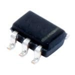
| 产品图片 |
|
| rohs | 符合RoHS无铅 / 符合限制有害物质指令(RoHS)规范要求 |
| 产品系列 | 放大器 IC,视频放大器,Texas Instruments OPA361AIDCKTG4- |
| 数据手册 | |
| 产品型号 | OPA361AIDCKTG4 |
| 产品 | Video Amplifiers |
| 产品目录页面 | |
| 产品种类 | 视频放大器 |
| 供应商器件封装 | SC-70-6 |
| 其它名称 | 296-18696-6 |
| 包装 | Digi-Reel® |
| 压摆率 | - |
| 商标 | Texas Instruments |
| 安装类型 | 表面贴装 |
| 安装风格 | SMD/SMT |
| 封装 | Reel |
| 封装/外壳 | 6-TSSOP,SC-88,SOT-363 |
| 封装/箱体 | SC-70-6 |
| 工作温度范围 | - 40 C to + 125 C |
| 工作电源电压 | 2.5 V to 3.6 V |
| 工厂包装数量 | 250 |
| 应用 | 通用 |
| 最大工作温度 | + 125 C |
| 最小工作温度 | - 40 C |
| 标准包装 | 1 |
| 电压-电源,单/双 (±) | 2.5 V ~ 3.3 V |
| 电流-电源 | 5.3mA |
| 电流-输出/通道 | 80mA |
| 电源电压-最大 | 3.3 V |
| 电源电压-最小 | 2.5 V |
| 电源电流 | 5.3 mA |
| 电源类型 | Single |
| 电路数 | 1 |
| 系列 | OPA361 |
| 输出类型 | 满摆幅 |
| 通道数量 | 1 Channel |


- 商务部:美国ITC正式对集成电路等产品启动337调查
- 曝三星4nm工艺存在良率问题 高通将骁龙8 Gen1或转产台积电
- 太阳诱电将投资9.5亿元在常州建新厂生产MLCC 预计2023年完工
- 英特尔发布欧洲新工厂建设计划 深化IDM 2.0 战略
- 台积电先进制程称霸业界 有大客户加持明年业绩稳了
- 达到5530亿美元!SIA预计今年全球半导体销售额将创下新高
- 英特尔拟将自动驾驶子公司Mobileye上市 估值或超500亿美元
- 三星加码芯片和SET,合并消费电子和移动部门,撤换高东真等 CEO
- 三星电子宣布重大人事变动 还合并消费电子和移动部门
- 海关总署:前11个月进口集成电路产品价值2.52万亿元 增长14.8%



PDF Datasheet 数据手册内容提取
OPA361 SBOS334A − SEPTEMBER 2005 − REVISED JANUARY 2006 3V VIDEO AMPLIFIER with Internal Gain and Filter in SC70 FEATURES DESCRIPTION (cid:1) EXCELLENT VIDEO PERFORMANCE The OPA361 high-speed amplifier is optimized for 3V (cid:1) INTERNAL GAIN: 5.2V/V portable video applications. It is specifically designed to be (cid:1) compatible with the video encoders embedded in Texas SUPPORTS TV-DETECTION (cid:1) Instruments’ OMAP2420 and DaVinci processors or other COMPATIBLE WITH OMAP242x and application processors with 0.5V video output. The input DAVINCI(cid:1) PROCESSORS PP common-mode range includes GND, which allows a (cid:1) 2-POLE RECONSTRUCTION FILTER video-DAC (digital-to-analog converter) to be DC-coupled (cid:1) to the OPA361. The TV-detection feature simplifies the INPUT RANGE INCLUDES GROUND end-user interface significantly by facilitating the − DC-Coupled Input (cid:1) automatic start/stop of video transmission. INTEGRATED LEVEL SHIFTER − DC-Coupled Output(1) The output swings within 5mV of GND and 250mV to V+ − No Output Capacitors Needed with a standard back-terminated video load (150Ω). An (cid:1) internal level shift circuit prevents the output from RAIL-TO-RAIL OUTPUT saturating with 0V input, thus preventing sync-pulse (cid:1) LOW QUIESCENT CURRENT: 5.3mA clipping in common video circuits. Therefore, the OPA361 (cid:1) SHUTDOWN CURRENT: 1.5(cid:1)A is ideally suited for DC-coupling to the video load. (cid:1) SINGLE-SUPPLY: 2.5V to 3.3V The OPA361 has been optimized for space-sensitive (cid:1) SC70-6 PACKAGE: 2.0mm x 2.1mm applications by integrating internal gain setting resistors (cid:1) (G = 5.2V/V) and a 2-pole video-DAC reconstruction filter. RoHS COMPLIANT (1)Internal circuitry avoids output saturation, even with 0V sync tip In shutdown mode, the quiescent current is reduced to level at the input video signal. < 1.5µA, dramatically reducing power consumption and prolonging battery life. APPLICATIONS The OPA361 is available in the tiny 2mm x 2.1mm SC70-6 (cid:1) package. CAMERA PHONES V+ RELATED LOW VOLTAGE VIDEO AMPS OPA361 10mV FEATURES PRODUCT +In 2F−iPlteorle 75Ω 2.7V to 3.3V, 70MHz, 6mA IQ, 5µA Sleep, SC70 OPA358 500Ω Out 2.7V to 3.3V, Filter, SAG, G = 2, 5µA Sleep, SC70 OPA360 2.7V to 5.5V, 200MHz, 300V/µs, 6µA Sleep, SOT23 OPA355 R 2.7V to 5.5V, 100MHz, 150V/µs, 6µA Sleep, SOT23 OPA357 SET 4kΩ G=5.2V/V Shutdown (seenote1) Enable Control GND (1)Closedwhenenabledduringnormaloperation;openwhenshutdown. Please be aware that an important notice concerning availability, standard warranty, and use in critical applications of TexasInstruments semiconductor products and disclaimers thereto appears at the end of this data sheet. DAVINCI is a registered trademark of Texas Instruments. All other trademarks are the property of their respective owners. (cid:1)(cid:2)(cid:3)(cid:4)(cid:5)(cid:6)(cid:7)(cid:8)(cid:3)(cid:9) (cid:4)(cid:10)(cid:7)(cid:10) (cid:11)(cid:12)(cid:13)(cid:14)(cid:15)(cid:16)(cid:17)(cid:18)(cid:11)(cid:14)(cid:12) (cid:11)(cid:19) (cid:20)(cid:21)(cid:15)(cid:15)(cid:22)(cid:12)(cid:18) (cid:17)(cid:19) (cid:14)(cid:13) (cid:23)(cid:21)(cid:24)(cid:25)(cid:11)(cid:20)(cid:17)(cid:18)(cid:11)(cid:14)(cid:12) (cid:26)(cid:17)(cid:18)(cid:22)(cid:27) (cid:1)(cid:15)(cid:14)(cid:26)(cid:21)(cid:20)(cid:18)(cid:19) Copyright 2005, Texas Instruments Incorporated (cid:20)(cid:14)(cid:12)(cid:13)(cid:14)(cid:15)(cid:16) (cid:18)(cid:14) (cid:19)(cid:23)(cid:22)(cid:20)(cid:11)(cid:13)(cid:11)(cid:20)(cid:17)(cid:18)(cid:11)(cid:14)(cid:12)(cid:19) (cid:23)(cid:22)(cid:15) (cid:18)(cid:28)(cid:22) (cid:18)(cid:22)(cid:15)(cid:16)(cid:19) (cid:14)(cid:13) (cid:7)(cid:22)(cid:29)(cid:17)(cid:19) (cid:8)(cid:12)(cid:19)(cid:18)(cid:15)(cid:21)(cid:16)(cid:22)(cid:12)(cid:18)(cid:19) (cid:19)(cid:18)(cid:17)(cid:12)(cid:26)(cid:17)(cid:15)(cid:26) (cid:30)(cid:17)(cid:15)(cid:15)(cid:17)(cid:12)(cid:18)(cid:31)(cid:27) (cid:1)(cid:15)(cid:14)(cid:26)(cid:21)(cid:20)(cid:18)(cid:11)(cid:14)(cid:12) (cid:23)(cid:15)(cid:14)(cid:20)(cid:22)(cid:19)(cid:19)(cid:11)(cid:12)! (cid:26)(cid:14)(cid:22)(cid:19) (cid:12)(cid:14)(cid:18) (cid:12)(cid:22)(cid:20)(cid:22)(cid:19)(cid:19)(cid:17)(cid:15)(cid:11)(cid:25)(cid:31) (cid:11)(cid:12)(cid:20)(cid:25)(cid:21)(cid:26)(cid:22) (cid:18)(cid:22)(cid:19)(cid:18)(cid:11)(cid:12)! (cid:14)(cid:13) (cid:17)(cid:25)(cid:25) (cid:23)(cid:17)(cid:15)(cid:17)(cid:16)(cid:22)(cid:18)(cid:22)(cid:15)(cid:19)(cid:27) www.ti.com
(cid:3)(cid:1)(cid:10)"#$ www.ti.com SBOS334A − SEPTEMBER 2005 − REVISED JANUARY 2006 ORDERING INFORMATION(1) PRODUCT PACKAGE PACKAGE DESIGNATOR PACKAGE MARKING OOPPAA336611 SSCC7700--66 DDCCKK AAUUYY (1)For the most current package and ordering information, see the Package Option Addendum at the end of this datasheet, or see the TI website at www.ti.com. This integrated circuit can be damaged by ESD. Texas Instruments recommends that all integrated circuits be handled with appropriate precautions. Failure to observe proper handling and installation procedures can cause damage. ESD damage can range from subtle performance degradation to complete device failure. Precision integrated circuits may be more susceptible to damage because very small parametric changes could cause the device not to meet its published specifications. ABSOLUTE MAXIMUM RATINGS(1) PIN CONFIGURATION Supply Voltage, V+ to V− . . . . . . . . . . . . . . . . . . . . . . . . . . . . . +3.6V Top View SC70 Signal Input Terminals, Voltage(2) . . . . . . . . −0.5V to (V+) + 0.5V Current(2) . . . . . . . . . . . . . . . . . . . ±10mA Output Short-Circuit through 75Ω to GND(3) . . . . . . . Continuous Operating Temperature . . . . . . . . . . . . . . . . . . . . . −40°C to +125°C Storage Temperature . . . . . . . . . . . . . . . . . . . . . . . −65°C to +150°C Junction Temperature. . . . . . . . . . . . . . . . . . . . . . . . . . . . . . . +160°C ESD Rating: +In 1 6 V+ A Human Body Model. . . . . . . . . . . . . . . . . . . . . . . . . . . . . . . 5000V GND 2 U 5 Enable Machine Model. . . . . . . . . . . . . . . . . . . . . . . . . . . . . . . . . . . . . 400V Y R 3 4 Out Charged Device Model . . . . . . . . . . . . . . . . . . . . . . . . . . . . 2000V SET (1)Stresses above these ratings may cause permanent damage. Exposure to absolute maximum conditions for extended periods may degrade device reliability. These are stress ratings only, and functional operation of the device at these or any other conditions beyond those specified is not implied. (2)Input terminals are diode-clamped to the power-supply rails. NOTE: The location of pin 1 on the OPA361 is determined by orienting Input signals that can swing more than 0.5V beyond the supply the package marking as shown in the diagram above. rails should be current-limited to 10mA or less. (3)Short-circuit to ground. 2
(cid:3)(cid:1)(cid:10)"#$ www.ti.com SBOS334A − SEPTEMBER 2005 − REVISED JANUARY 2006 ELECTRICAL CHARACTERISTICS: V = +2.5V to +3.3V S Boldface limits apply over the temperature range, T = −40°C to +125°C. A At TA = +25°C, RL = 150Ω connected to GND, unless otherwise noted. OPA361 PARAMETER CONDITIONS MIN TYP MAX UNITS OFFSET LEVEL-SHIFT VOLTAGE Output Level-Shift Voltage(1) VOLS VS = +2.8V, VIN = GND −3 11 55 mV Over Temperature 20 mV vs Power Supply PSRR VS = +2.5V to +3.3V ±80 µV/V INPUT VOLTAGE RANGE Input Voltage Range(2) VCM VS = 2.5V GND 0.42 V VS = 2.8V GND 0.48 V VS = 3.3V GND 0.55 V Input Resistance (+In) RIN 450 510 550 Ω RSET Resistance RSET 3600 4070 4400 Ω Matching of RIN and RSET 2 0.5 % VOLTAGE GAIN ∆VOUT/∆VIN, VS = +2.5V, VINMIN = 0V, VINMAX = 0.42V 5.06 5.17 5.28 V/V ∆VOUT/∆VIN, VS = +2.8V, VINMIN = 0V, VINMAX = 0.48V 5.06 5.17 5.28 V/V ∆VOUT/∆VIN, VS = +3.3V, VINMIN = 0V, VINMAX = 0.55V 5.06 5.17 5.28 V/V FREQUENCY RESPONSE Filter Response Cutoff Frequency f−3dB 9 MHz Normalized Gain: fIN = 4.5MHz VO = 2VPP −0.1 dB fIN = 27MHz VO = 2VPP −18 dB fIN = 54MHz VO = 2VPP −23 dB Differential Gain Error RL = 150Ω 1.2 % Differential Phase Error RL = 150Ω 1.6 degrees Group Delay Variation 100kHz, 4.5MHz 26 ns Signal-to-Noise Ratio SNR 100% White Signal 65 dB OUTPUT Positive Voltage Output Swing from Rail VS = +2.8V, VIN = 0.7V, RL = 150Ω to GND 130 250 mV Negative Voltage Output Swing from Rail VS = +2.8V, VIN = −0.05V, RL = 150Ω to GND 0.15 5 mV Positive Voltage Output Swing from Rail VS = +2.8V, VIN = 0.7V, RL = 75Ω to GND 260 mV Negative Voltage Output Swing from Rail VS = +2.8V, VIN = −0.05V, RL = 75Ω to GND 2 mV Output Leakage VS = +2.8V, Disabled, VO = 2V 0.3 100 nA Output Current(3) IO VS = +2.8V ±80 mA POWER SUPPLY Specified Voltage Range VS 2.5 3.3 V Quiescent Current IQ VS = +2.8V, Enabled, IO = 0, VOUT = 1.4V 5.3 7.5 mA Over Temperature Specified Temperature Range 9 mA ENABLE/SHUTDOWN FUNCTION Disabled (logic-LOW threshold) 0 0.35 V Enabled (logic-HIGH threshold) 1.3 VS V Enable Time 1.5 µs Disable Time 50 ns Shutdown Current VS = +2.8V, Disabled 1.5 3 µA TEMPERATURE RANGE Specified/Operating Range −40 +125 °C Storage Range −65 +150 °C Thermal Resistance (cid:1)JA SC70 250 °C/W (1) Output referred. (2) Limited by output swing and internal G = 5.2V/V. (3) See typical characteristics Output Voltage Swing vs Output Current. 3
(cid:3)(cid:1)(cid:10)"#$ www.ti.com SBOS334A − SEPTEMBER 2005 − REVISED JANUARY 2006 TYPICAL CHARACTERISTICS: V = 2.8V S At TA = +25°C and RL = 150Ω, unless otherwise noted. R vsTEMPERATURE R vsTEMPERATURE IN SET 535 4250 530 4200 525 4150 520 Ω) Ω) (N515 (ET4100 RI RS 510 4050 505 4000 500 495 3950 −50 −25 0 +25 +50 +75 +100 +125 +150 −50 −25 0 +25 +50 +75 +100 +125 +150 Temperature((cid:2)C) Temperature((cid:2)C) R /R RATIO GAIN SET IN vsTEMPERATURE vsTEMPERATURE 8.5 5.5 8.4 8.3 5.4 8.2 o RRatiIN 88..10 n(V/V) 5.3 /SET 7.9 Gai 5.2 R 7.8 7.7 5.1 7.6 7.5 5.0 −50 −25 0 +25 +50 +75 +100 +125 +150 −50 −25 0 +25 +50 +75 +100 +125 +150 Temperature((cid:2)C) Temperature((cid:2)C) OUTPUTVOLTAGE OUTPUTVOLTAGE vsTEMPERATURE vsTEMPERATURE 0.005 2.80 VIN=−50mV VIN=700mV VS=2.8V 2.75 VS=2.8V 0.004 (V) (V) 2.70 ge 0.003 ge a a olt olt 2.65 V V ut 0.002 ut p p ut ut 2.60 O O 0.001 2.55 0 2.50 −50 −25 0 +25 +50 +75 +100 +125 +150 −50 −25 0 +25 +50 +75 +100 +125 +150 Temperature((cid:2)C) Temperature((cid:2)C) 4
(cid:3)(cid:1)(cid:10)"#$ www.ti.com SBOS334A − SEPTEMBER 2005 − REVISED JANUARY 2006 TYPICAL CHARACTERISTICS: V = 2.8V (continued) S At TA = +25°C and RL = 150Ω, unless otherwise noted. V LEVELSHIFT QUIESCENTCURRENT OUT vsTEMPERATURE vsTEMPERATURE 0.05 9 V =2.8V S V =0V 0.04 IN 8 A) V) m ( 0.03 ( 7 hift ent elS 0.02 Curr 6 v Le ent UT0.01 sc 5 O e V ui Q 0 4 −0.01 3 −50 −25 0 +25 +50 +75 +100 +125 +150 −50 −25 0 +25 +50 +75 +100 +125 +150 Temperature((cid:2)C) Temperature((cid:2)C) OUTPUTLEAKAGECURRENT OUTPUTLEAKAGE vsTEMPERATURE INSHUTDOWN 1000000 400 Enable=0V Enable=0V pA) 100000 VPULLUP=1.8V pA) 335000 ( ( nt 10000 nt 250 e e urr urr 200 C 1000 C ge ge 150 aka 100 aka 100 e e L L ut 10 ut 50 p p ut ut 0 O 1 O −50 0.1 −100 −50 −25 0 +25 +50 +75 +100 +125 +150 0 0.5 1 1.5 2 2.5 3 Temperature((cid:2)C) V (V) PULLUP SHUTDOWNQUIESCENTCURRENTHYSTERESIS ACRESPONSE vsTEMPERATURE ATVARIOUSTEMPERATURES 10000 3 0 −3 (mA)SHDN1010000 +−2450(cid:2)(cid:2)CC esponse(dB) −−−−116925 +125(cid:2)C IQ +125(cid:2)C ACR −−1281 10 +85(cid:2)C −24 +25(cid:2)C −27 −40(cid:2)C 1 −30 0.7 0.75 0.8 0.85 0.9 0.95 1 100k 1M 10M 100M V (V) Frequency(Hz) SHDN 5
(cid:3)(cid:1)(cid:10)"#$ www.ti.com SBOS334A − SEPTEMBER 2005 − REVISED JANUARY 2006 TYPICAL CHARACTERISTICS: V = 2.8V (continued) S At TA = +25°C and RL = 150Ω, unless otherwise noted. TURN−ONTIME TURN−OFFTIME v) v) di di V/ V/ m m 0 0 0 0 5 5 ( ( e e g g a a olt olt V V Time(1µs/div) Time(25ns/div) OUTPUTVOLTAGE GROUPDELAY vsOUTPUTCURRENT vsFREQUENCY 3.0 100 90 2.5 80 2.0 ns) 70 V) ay( 60 (UT 1.5 Del 50 VO up 40 o 1.0 Gr 30 +125(cid:2)C +85(cid:2)C +25(cid:2)C 0(cid:2)C −25(cid:2)C −40(cid:2)C 20 0.5 10 0 0 0 1 2 3 4 5 6 7 8 9 0 1 2 3 4 5 100k 1M 10M 100M 0 0 0 0 0 0 0 0 0 1 1 1 1 1 1 0. 0. 0. 0. 0. 0. 0. 0. 0. 0. 0. 0. 0. 0. 0. Frequency(Hz) I (A) OUT DIFFERENTIALGAIN INP = A − C SYNC = INT MTIME = 10s LINE = 330 −5 0 +5 DG1 −0.6 %1 DG2 −1.0 %. DG3 −1.1 %. DG4 −1.2 %. DG5 −0.8 %5 STEPS ZOOM MODE 4 5 0 1 2 1 DIFFERENTIALPHASE INP = A − C SYNC = INT MTIME = 10s LINE = 330 −5 0 +5 DP1 1.1 dg1 DP2 1.6 dg. DP3 1.6 dg. DP4 1.5 dg. DP5 1.1 dg5 STEPS ZOOM MODE 4 5 0 1 2 1 6
(cid:3)(cid:1)(cid:10)"#$ www.ti.com SBOS334A − SEPTEMBER 2005 − REVISED JANUARY 2006 APPLICATIONS INFORMATION helps to automate start/stop operation of the TV-out function and minimizes power consumption. The OPA361 video amplifier has been optimized to fit (cid:1) A 2-pole filter is incorporated for DAC signal seamlessly with Texas Instruments’ OMAP242x reconstruction. Multimedia processor. The following features have been (cid:1) integrated to provide excellent video performance. The OPA361 employs an internal level shift circuit (cid:1) that avoids sync pulse clipping and allows Internal gain setting resistors (G = 5.2V/V) reduce DC-coupled output. the number of external components needed in the (cid:1) video circuit. A shutdown feature reduces quiescent current to (cid:1) Integration of the 500Ω video encoder load resistor less than 1.5µA—crucial for portable applications and 4kΩ R resistor used by the OMAP242x Although OPA361 is optimized for the OMAP242x SET helps minimize the number of external components processor, it is also suitable to interface with any digital and also ensures excellent ratio and temperature media processor that outputs a video signal on the order tracking. This feature helps to keep the overall gain of 0.4VPP to 0.5VPP. accurate and stable over temperature. Figure 1 shows a typical application drawing with the (cid:1) TV-detection support in connection with an OMAP242x processor and the TWL92230 Energy OMAP242x multimedia processor. This feature Management Chip. TWL92230 1.8VDAC 0.5VV RegulatorV REF AUX V+ 2.8V 1.8V OMAP2420 OPA361 Pull−Up 10mV 10kΩ Video +In 2−Pole 75Ω DAC Filter Out + 500Ω 75Ω R SET 4kΩ G=5.2V/V Enable Shutdown (seenote1) TVDetect Control GPIO(3) GND 100kΩ(2) TVDetect GPIO (1)Closedwhenenabledduringnormaloperation;openwhenshutdown. (2)ProtectsGPIOagainstovervoltageconditionsduringactivevideotransmission. (3)GPIOmustbeabletogenerateaninterrupt. Figure 1. Typical Application using the OMAP242x and the TWL92230 7
(cid:3)(cid:1)(cid:10)"#$ www.ti.com SBOS334A − SEPTEMBER 2005 − REVISED JANUARY 2006 OPERATING VOLTAGE The Enable logic input voltage is referenced to the OPA361 GND pin. A logic level HIGH applied to the enable The OPA361 is fully specified from 2.5V to 3.3V over a pin enables the op amp. The logic levels are compatible temperature range of −40(cid:2)C to +125(cid:2)C. Parameters that with 1.8V CMOS logic levels. A valid logic HIGH is defined vary significantly with operating voltages or temperature as > 1.3V above GND. A valid logic LOW is defined as are shown in the Typical Characteristics. Power-supply < 0.35V above GND. If the Enable pin is not connected, pins should be bypassed with 100nF ceramic capacitors. internal pull-up circuitry will enable the amplifier. When disabling the OPA361, internal circuitry also INPUT VOLTAGE disconnects the internal gain setting feedback. This feature is in support of the TV-detection function. See the The input common-mode range of the OPA361 series TV-Detect Function section for more detailed information. extends from GND to 0.55V on a 3.3V supply. The input range is limited by the internal gain in conjunction with the maximum output swing capability and the power-supply INTERNAL 2-POLE FILTER voltage. The OPA361 filter is a Sallen-Key topology with a 9MHz cutoff frequency. Figure 2 shows a detailed drawing of the INPUT OVERVOLTAGE PROTECTION filter components. This filter allows video signals to pass without any visible distortion, as shown in Figure 3 through All OPA361 pins are static-protected with internal ESD Figure 6. The video encoder embedded in the OMAP242x protection diodes connected to the supplies. These diodes processor typically samples at 54MHz. At this frequency, will provide input overdrive protection if the current is the attenuation is typically 23dB, which effectively externally limited to 10mA. attenuates the sampling aliases. The internal 500Ω resistor on the input to GND converts ENABLE/SHUTDOWN the output current of the OMAP2420 internal video DAC into a voltage. It is also part of the Sallen-Key filter. Using The OPA361 has a shutdown feature that disables the an external resistor to adjust the input voltage range will output and reduces the quiescent current to less than also alter the filter characteristics. 1.5µA. This feature is especially useful for portable video applications, where the device is infrequently connected to a television (TV) or other video device. OPA361 3.6pF 2.2kΩ 2.2kΩ Television ( ) V 75Ω O 500Ω 12.5pF 75Ω 4.22kΩ 1kΩ Figure 2. Filter Structure of the OPA361 8
(cid:3)(cid:1)(cid:10)"#$ www.ti.com SBOS334A − SEPTEMBER 2005 − REVISED JANUARY 2006 Video Performance The multiburst test patterns have different sine-wave burst sections with the following frequencies: 0.5MHz, 1MHz, The color bar signal in Figure 3 shows excellent amplitude 2MHz, 4MHz, 4.8MHz and 5.8MHz with 420mV . There PP characteristics and no attenuation of colors with respect to is no visible attenuation even at the highest frequencies, the luminance signal. which indicates a very flat frequency response of the OPA361. As shown in Figure 5 and Figure 6, the top line illustrates the full signal and the bottom line is a more detailed view of the last three sine wave bursts. ∆: 2.02V @: 30.0mV Figure 3. 100/75 Color Bar Signal at Output of OPA361 Figure 5. Multiburst Signal (CCIR 18/1) Shows The CCIR330/5 test pattern requires one of the greatest Very Flat Frequency Response dynamic ranges, and therefore tests the OPA361 output voltage swing capability. The scope plot shown in Figure 4 has been taken with a 2.8V supply and shows no clipping The CCIR17 test pattern contains a 2T and a 20T pulse, on the top side of the signal. as shown in Figure 6. The 2T pulse is used to check for pulse distortion and reflection, and the 20T pulse is used to check for amplitude and group delay between chrominance and luminance. Neither pulse exhibits any ∆:2.30V distortion or group delay artifacts. @:2.31mV Figure 4. CCIR330/5: No Clipping, Even On 2.8V Supply Figure 6. CCIR 17 2T and 20T Pulses Show No Visible Distortion 9
(cid:3)(cid:1)(cid:10)"#$ www.ti.com SBOS334A − SEPTEMBER 2005 − REVISED JANUARY 2006 INTERNAL LEVEL SHIFT voltage level is pulled LOW if the TV (or other video equipment) is connected, or HIGH if nothing is connected. Many common video DACs embedded in digital media A GPIO in the processor can be used to read this logic level processors, like the new OMAP242x processors, operate and decide if a video load is connected. Figure 8 shows a on a single supply (no negative supply). Typically, the scope plot with the TV disconnected and Figure 9 shows lowest point of the sync pulse output by these video DACs a scope plot with the TV connected; the upper line in both is close to 0V. With a 0V input, the output of a common figures is the disable pulse. Figure 10 shows a circuit single-supply op amp saturates at a voltage > 0V. This drawing using the TV-detect signal to disable or enable the effect would clip the sync pulse, and therefore degrade the OPA361. video signal integrity. The OPA361 employs an internal level shift circuit to avoid clipping. The input signal is typically shifted by approximately 11mV. This shift is well within the linear output voltage range of the OPA361 with a standard 150Ω video load. OPA361DisablePulse ∆: 1.84V Output Swing Capability @: 1.84V Figure 7 shows the true output swing capability of the OPA361 by taking the tip of the input sync pulse to a OPA361Ouput PulledHIGH; slightly negative voltage. Even when the output sync tip is NoVideoLoad at 3mV, the output after the 75Ω series termination still Connected shows no clipping of the sync pulse. EquilizationPulses 1stVerticalSyncPulse VerticalSyncPulses ∆: 305mV @: 3.00mV Figure 8. Output of OPA361 Pulled Up To 1.8V During Disable: TV Disconnected OPA361DisablePulse Figure 7. No Clipping of the Sync Pulse OPA361OuputPulledLOW DuetoVideoLoad TV-Detect Function The TV-detection feature of the OPA361 works in EquilizationPulses 1stVerticalSyncPulse conjunction with the OMAP242x (or other processors) to VerticalSyncPulses detect if a television is connected to the video output of the device. In order to detect a TV load, the OPA361 is briefly turned off, ideally during the first vertical sync pulse. For Figure 9. Output of OPA361 Pulled Down: the detection, a simple pull-up resistor to the processor TV Connected. logic supply is used on the output of the OPA361. The 10
(cid:3)(cid:1)(cid:10)"#$ www.ti.com SBOS334A − SEPTEMBER 2005 − REVISED JANUARY 2006 TWL92230 1.8VDAC 0.5VV RegulatorV REF AUX V+ 2.5Vor2.8V 1.8V OMAP2420 OPA361 Pull−Up 10mV 10kΩ Video +In 2−Pole 75Ω DAC Filter Out + 500Ω 75Ω R SET 4kΩ G=5.2V/V Enable Shutdown (seenote1) TVDetect Control GPIO(3) GND 100kΩ(2) TVDetect GPIO (1)Closedwhenenabledduringnormaloperation;openwhenshutdown. (2)ProtectsGPIOagainstovervoltageconditionsduringactivevideotransmission. (3)GPIOmustbeabletogenerateinterrupt. Figure 10. Using TV-Detect Signal to Disable/Enable the OPA361 Disabling the OPA361 also disconnects the internal The following functionality can be achieved by feedback resistors’ path to GND, and therefore there is no implementing TV-detection: current flowing from the logic supply through the pull-up (cid:1) Automatic video start by polling the video line resistor to GND if no video load is connected; this helps to periodically. conserve battery life. The typical leakage when the output is pulled high and OPA361 is disabled is only about 300pA. (cid:1) Automatic video stop if the TV (or other equipment) is disconnected. Proper implementation allows to significantly simplify the user interface. For more information, see Application Report SBOA109, OPA361 and TV Detection, available for download at www.ti.com. 11
PACKAGE OPTION ADDENDUM www.ti.com 24-Aug-2018 PACKAGING INFORMATION Orderable Device Status Package Type Package Pins Package Eco Plan Lead/Ball Finish MSL Peak Temp Op Temp (°C) Device Marking Samples (1) Drawing Qty (2) (6) (3) (4/5) OPA361AIDCKR ACTIVE SC70 DCK 6 3000 Green (RoHS CU NIPDAU Level-2-260C-1 YEAR -40 to 125 AUY & no Sb/Br) OPA361AIDCKT ACTIVE SC70 DCK 6 250 Green (RoHS CU NIPDAU Level-2-260C-1 YEAR -40 to 125 AUY & no Sb/Br) OPA361AIDCKTG4 ACTIVE SC70 DCK 6 250 Green (RoHS CU NIPDAU Level-2-260C-1 YEAR -40 to 125 AUY & no Sb/Br) (1) The marketing status values are defined as follows: ACTIVE: Product device recommended for new designs. LIFEBUY: TI has announced that the device will be discontinued, and a lifetime-buy period is in effect. NRND: Not recommended for new designs. Device is in production to support existing customers, but TI does not recommend using this part in a new design. PREVIEW: Device has been announced but is not in production. Samples may or may not be available. OBSOLETE: TI has discontinued the production of the device. (2) RoHS: TI defines "RoHS" to mean semiconductor products that are compliant with the current EU RoHS requirements for all 10 RoHS substances, including the requirement that RoHS substance do not exceed 0.1% by weight in homogeneous materials. Where designed to be soldered at high temperatures, "RoHS" products are suitable for use in specified lead-free processes. TI may reference these types of products as "Pb-Free". RoHS Exempt: TI defines "RoHS Exempt" to mean products that contain lead but are compliant with EU RoHS pursuant to a specific EU RoHS exemption. Green: TI defines "Green" to mean the content of Chlorine (Cl) and Bromine (Br) based flame retardants meet JS709B low halogen requirements of <=1000ppm threshold. Antimony trioxide based flame retardants must also meet the <=1000ppm threshold requirement. (3) MSL, Peak Temp. - The Moisture Sensitivity Level rating according to the JEDEC industry standard classifications, and peak solder temperature. (4) There may be additional marking, which relates to the logo, the lot trace code information, or the environmental category on the device. (5) Multiple Device Markings will be inside parentheses. Only one Device Marking contained in parentheses and separated by a "~" will appear on a device. If a line is indented then it is a continuation of the previous line and the two combined represent the entire Device Marking for that device. (6) Lead/Ball Finish - Orderable Devices may have multiple material finish options. Finish options are separated by a vertical ruled line. Lead/Ball Finish values may wrap to two lines if the finish value exceeds the maximum column width. Important Information and Disclaimer:The information provided on this page represents TI's knowledge and belief as of the date that it is provided. TI bases its knowledge and belief on information provided by third parties, and makes no representation or warranty as to the accuracy of such information. Efforts are underway to better integrate information from third parties. TI has taken and continues to take reasonable steps to provide representative and accurate information but may not have conducted destructive testing or chemical analysis on incoming materials and chemicals. TI and TI suppliers consider certain information to be proprietary, and thus CAS numbers and other limited information may not be available for release. Addendum-Page 1
PACKAGE OPTION ADDENDUM www.ti.com 24-Aug-2018 In no event shall TI's liability arising out of such information exceed the total purchase price of the TI part(s) at issue in this document sold by TI to Customer on an annual basis. OTHER QUALIFIED VERSIONS OF OPA361 : •Automotive: OPA361-Q1 NOTE: Qualified Version Definitions: •Automotive - Q100 devices qualified for high-reliability automotive applications targeting zero defects Addendum-Page 2
PACKAGE MATERIALS INFORMATION www.ti.com 3-Aug-2017 TAPE AND REEL INFORMATION *Alldimensionsarenominal Device Package Package Pins SPQ Reel Reel A0 B0 K0 P1 W Pin1 Type Drawing Diameter Width (mm) (mm) (mm) (mm) (mm) Quadrant (mm) W1(mm) OPA361AIDCKR SC70 DCK 6 3000 179.0 8.4 2.2 2.5 1.2 4.0 8.0 Q3 OPA361AIDCKR SC70 DCK 6 3000 178.0 9.0 2.4 2.5 1.2 4.0 8.0 Q3 OPA361AIDCKT SC70 DCK 6 250 179.0 8.4 2.25 2.4 1.22 4.0 8.0 Q3 OPA361AIDCKT SC70 DCK 6 250 178.0 9.0 2.4 2.5 1.2 4.0 8.0 Q3 PackMaterials-Page1
PACKAGE MATERIALS INFORMATION www.ti.com 3-Aug-2017 *Alldimensionsarenominal Device PackageType PackageDrawing Pins SPQ Length(mm) Width(mm) Height(mm) OPA361AIDCKR SC70 DCK 6 3000 195.0 200.0 45.0 OPA361AIDCKR SC70 DCK 6 3000 180.0 180.0 18.0 OPA361AIDCKT SC70 DCK 6 250 195.0 200.0 45.0 OPA361AIDCKT SC70 DCK 6 250 180.0 180.0 18.0 PackMaterials-Page2
None
None
IMPORTANTNOTICE TexasInstrumentsIncorporated(TI)reservestherighttomakecorrections,enhancements,improvementsandotherchangestoits semiconductorproductsandservicesperJESD46,latestissue,andtodiscontinueanyproductorserviceperJESD48,latestissue.Buyers shouldobtainthelatestrelevantinformationbeforeplacingordersandshouldverifythatsuchinformationiscurrentandcomplete. TI’spublishedtermsofsaleforsemiconductorproducts(http://www.ti.com/sc/docs/stdterms.htm)applytothesaleofpackagedintegrated circuitproductsthatTIhasqualifiedandreleasedtomarket.AdditionaltermsmayapplytotheuseorsaleofothertypesofTIproductsand services. ReproductionofsignificantportionsofTIinformationinTIdatasheetsispermissibleonlyifreproductioniswithoutalterationandis accompaniedbyallassociatedwarranties,conditions,limitations,andnotices.TIisnotresponsibleorliableforsuchreproduced documentation.Informationofthirdpartiesmaybesubjecttoadditionalrestrictions.ResaleofTIproductsorserviceswithstatements differentfromorbeyondtheparametersstatedbyTIforthatproductorservicevoidsallexpressandanyimpliedwarrantiesforthe associatedTIproductorserviceandisanunfairanddeceptivebusinesspractice.TIisnotresponsibleorliableforanysuchstatements. BuyersandotherswhoaredevelopingsystemsthatincorporateTIproducts(collectively,“Designers”)understandandagreethatDesigners remainresponsibleforusingtheirindependentanalysis,evaluationandjudgmentindesigningtheirapplicationsandthatDesignershave fullandexclusiveresponsibilitytoassurethesafetyofDesigners'applicationsandcomplianceoftheirapplications(andofallTIproducts usedinorforDesigners’applications)withallapplicableregulations,lawsandotherapplicablerequirements.Designerrepresentsthat,with respecttotheirapplications,Designerhasallthenecessaryexpertisetocreateandimplementsafeguardsthat(1)anticipatedangerous consequencesoffailures,(2)monitorfailuresandtheirconsequences,and(3)lessenthelikelihoodoffailuresthatmightcauseharmand takeappropriateactions.DesigneragreesthatpriortousingordistributinganyapplicationsthatincludeTIproducts,Designerwill thoroughlytestsuchapplicationsandthefunctionalityofsuchTIproductsasusedinsuchapplications. TI’sprovisionoftechnical,applicationorotherdesignadvice,qualitycharacterization,reliabilitydataorotherservicesorinformation, including,butnotlimitedto,referencedesignsandmaterialsrelatingtoevaluationmodules,(collectively,“TIResources”)areintendedto assistdesignerswhoaredevelopingapplicationsthatincorporateTIproducts;bydownloading,accessingorusingTIResourcesinany way,Designer(individuallyor,ifDesignerisactingonbehalfofacompany,Designer’scompany)agreestouseanyparticularTIResource solelyforthispurposeandsubjecttothetermsofthisNotice. TI’sprovisionofTIResourcesdoesnotexpandorotherwisealterTI’sapplicablepublishedwarrantiesorwarrantydisclaimersforTI products,andnoadditionalobligationsorliabilitiesarisefromTIprovidingsuchTIResources.TIreservestherighttomakecorrections, enhancements,improvementsandotherchangestoitsTIResources.TIhasnotconductedanytestingotherthanthatspecifically describedinthepublisheddocumentationforaparticularTIResource. Designerisauthorizedtouse,copyandmodifyanyindividualTIResourceonlyinconnectionwiththedevelopmentofapplicationsthat includetheTIproduct(s)identifiedinsuchTIResource.NOOTHERLICENSE,EXPRESSORIMPLIED,BYESTOPPELOROTHERWISE TOANYOTHERTIINTELLECTUALPROPERTYRIGHT,ANDNOLICENSETOANYTECHNOLOGYORINTELLECTUALPROPERTY RIGHTOFTIORANYTHIRDPARTYISGRANTEDHEREIN,includingbutnotlimitedtoanypatentright,copyright,maskworkright,or otherintellectualpropertyrightrelatingtoanycombination,machine,orprocessinwhichTIproductsorservicesareused.Information regardingorreferencingthird-partyproductsorservicesdoesnotconstitutealicensetousesuchproductsorservices,orawarrantyor endorsementthereof.UseofTIResourcesmayrequirealicensefromathirdpartyunderthepatentsorotherintellectualpropertyofthe thirdparty,oralicensefromTIunderthepatentsorotherintellectualpropertyofTI. TIRESOURCESAREPROVIDED“ASIS”ANDWITHALLFAULTS.TIDISCLAIMSALLOTHERWARRANTIESOR REPRESENTATIONS,EXPRESSORIMPLIED,REGARDINGRESOURCESORUSETHEREOF,INCLUDINGBUTNOTLIMITEDTO ACCURACYORCOMPLETENESS,TITLE,ANYEPIDEMICFAILUREWARRANTYANDANYIMPLIEDWARRANTIESOF MERCHANTABILITY,FITNESSFORAPARTICULARPURPOSE,ANDNON-INFRINGEMENTOFANYTHIRDPARTYINTELLECTUAL PROPERTYRIGHTS.TISHALLNOTBELIABLEFORANDSHALLNOTDEFENDORINDEMNIFYDESIGNERAGAINSTANYCLAIM, INCLUDINGBUTNOTLIMITEDTOANYINFRINGEMENTCLAIMTHATRELATESTOORISBASEDONANYCOMBINATIONOF PRODUCTSEVENIFDESCRIBEDINTIRESOURCESOROTHERWISE.INNOEVENTSHALLTIBELIABLEFORANYACTUAL, DIRECT,SPECIAL,COLLATERAL,INDIRECT,PUNITIVE,INCIDENTAL,CONSEQUENTIALOREXEMPLARYDAMAGESIN CONNECTIONWITHORARISINGOUTOFTIRESOURCESORUSETHEREOF,ANDREGARDLESSOFWHETHERTIHASBEEN ADVISEDOFTHEPOSSIBILITYOFSUCHDAMAGES. UnlessTIhasexplicitlydesignatedanindividualproductasmeetingtherequirementsofaparticularindustrystandard(e.g.,ISO/TS16949 andISO26262),TIisnotresponsibleforanyfailuretomeetsuchindustrystandardrequirements. WhereTIspecificallypromotesproductsasfacilitatingfunctionalsafetyorascompliantwithindustryfunctionalsafetystandards,such productsareintendedtohelpenablecustomerstodesignandcreatetheirownapplicationsthatmeetapplicablefunctionalsafetystandards andrequirements.Usingproductsinanapplicationdoesnotbyitselfestablishanysafetyfeaturesintheapplication.Designersmust ensurecompliancewithsafety-relatedrequirementsandstandardsapplicabletotheirapplications.DesignermaynotuseanyTIproductsin life-criticalmedicalequipmentunlessauthorizedofficersofthepartieshaveexecutedaspecialcontractspecificallygoverningsuchuse. Life-criticalmedicalequipmentismedicalequipmentwherefailureofsuchequipmentwouldcauseseriousbodilyinjuryordeath(e.g.,life support,pacemakers,defibrillators,heartpumps,neurostimulators,andimplantables).Suchequipmentincludes,withoutlimitation,all medicaldevicesidentifiedbytheU.S.FoodandDrugAdministrationasClassIIIdevicesandequivalentclassificationsoutsidetheU.S. TImayexpresslydesignatecertainproductsascompletingaparticularqualification(e.g.,Q100,MilitaryGrade,orEnhancedProduct). Designersagreethatithasthenecessaryexpertisetoselecttheproductwiththeappropriatequalificationdesignationfortheirapplications andthatproperproductselectionisatDesigners’ownrisk.Designersaresolelyresponsibleforcompliancewithalllegalandregulatory requirementsinconnectionwithsuchselection. DesignerwillfullyindemnifyTIanditsrepresentativesagainstanydamages,costs,losses,and/orliabilitiesarisingoutofDesigner’snon- compliancewiththetermsandprovisionsofthisNotice. MailingAddress:TexasInstruments,PostOfficeBox655303,Dallas,Texas75265 Copyright©2018,TexasInstrumentsIncorporated
 Datasheet下载


