ICGOO在线商城 > OPA234E/250

 Datasheet下载
- 型号: OPA234E/250
- 制造商: Texas Instruments
- 库位|库存: xxxx|xxxx
- 要求:
| 数量阶梯 | 香港交货 | 国内含税 |
| +xxxx | $xxxx | ¥xxxx |
查看当月历史价格
查看今年历史价格
OPA234E/250产品简介:
ICGOO电子元器件商城为您提供OPA234E/250由Texas Instruments设计生产,在icgoo商城现货销售,并且可以通过原厂、代理商等渠道进行代购。 提供OPA234E/250价格参考以及Texas InstrumentsOPA234E/250封装/规格参数等产品信息。 你可以下载OPA234E/250参考资料、Datasheet数据手册功能说明书, 资料中有OPA234E/250详细功能的应用电路图电压和使用方法及教程。
| 参数 | 数值 |
| -3db带宽 | - |
| 产品目录 | 集成电路 (IC)半导体 |
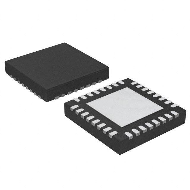
| 描述 | IC OPAMP GP 350KHZ 8VSSOP运算放大器 - 运放 Low Power Prec Sngl-Sply Oper Amp |
| 产品分类 | Linear - Amplifiers - Instrumentation, OP Amps, Buffer Amps集成电路 - IC |
| 品牌 | Texas Instruments |
| 产品手册 | |
| 产品图片 |
|
| rohs | 符合RoHS无铅 / 符合限制有害物质指令(RoHS)规范要求 |
| 产品系列 | 放大器 IC,运算放大器 - 运放,Texas Instruments OPA234E/250- |
| 数据手册 | |
| 产品型号 | OPA234E/250 |
| 产品目录页面 | |
| 产品种类 | 运算放大器 - 运放 |
| 供应商器件封装 | 8-VSSOP |
| 共模抑制比—最小值 | 91 dB |
| 关闭 | No Shutdown |
| 其它名称 | OPA234EDKR |
| 包装 | Digi-Reel® |
| 单位重量 | 26 mg |
| 压摆率 | 0.2 V/µs |
| 双重电源电压 | +/- 3 V, +/- 5 V, +/- 9 V |
| 商标 | Texas Instruments |
| 增益带宽生成 | 0.35 MHz |
| 增益带宽积 | 350kHz |
| 安装类型 | 表面贴装 |
| 安装风格 | SMD/SMT |
| 封装 | Reel |
| 封装/外壳 | 8-TSSOP,8-MSOP(0.118",3.00mm 宽) |
| 封装/箱体 | VSSOP-8 |
| 工作温度 | -40°C ~ 85°C |
| 工作电源电压 | 2.7 V to 36 V, +/- 1.35 V to +/- 18 V |
| 工厂包装数量 | 250 |
| 技术 | Bipolar |
| 放大器类型 | 通用 |
| 最大双重电源电压 | +/- 18 V |
| 最大工作温度 | + 125 C |
| 最小双重电源电压 | +/- 1.35 V |
| 最小工作温度 | - 40 C |
| 标准包装 | 1 |
| 电压-电源,单/双 (±) | 2.7 V ~ 36 V, ±1.35 V ~ 18 V |
| 电压-输入失调 | 70µV |
| 电流-电源 | 275µA |
| 电流-输入偏置 | 12nA |
| 电流-输出/通道 | 22mA |
| 电源电流 | 0.35 mA |
| 电路数 | 1 |
| 系列 | OPA234 |
| 设计资源 | http://www.digikey.com/product-highlights/cn/zh/texas-instruments-webench-design-center/3176 |
| 转换速度 | 0.2 V/us |
| 输入偏压电流—最大 | 30 nA |
| 输入参考电压噪声 | 25 nV |
| 输入补偿电压 | 150 uV |
| 输出类型 | - |
| 通道数量 | 1 Channel |


- 商务部:美国ITC正式对集成电路等产品启动337调查
- 曝三星4nm工艺存在良率问题 高通将骁龙8 Gen1或转产台积电
- 太阳诱电将投资9.5亿元在常州建新厂生产MLCC 预计2023年完工
- 英特尔发布欧洲新工厂建设计划 深化IDM 2.0 战略
- 台积电先进制程称霸业界 有大客户加持明年业绩稳了
- 达到5530亿美元!SIA预计今年全球半导体销售额将创下新高
- 英特尔拟将自动驾驶子公司Mobileye上市 估值或超500亿美元
- 三星加码芯片和SET,合并消费电子和移动部门,撤换高东真等 CEO
- 三星电子宣布重大人事变动 还合并消费电子和移动部门
- 海关总署:前11个月进口集成电路产品价值2.52万亿元 增长14.8%


PDF Datasheet 数据手册内容提取
OPA234 OPA2234 OPA234 OPA234 OPA2234 OPA4234 OPA4234 SBOS055B – MAY 1996 – REVISED APRIL 2008 Low-Power, Precision SINGLE-SUPPLY OPERATIONAL AMPLIFIERS FEATURES OPA234 (cid:1) WIDE SUPPLY RANGE: Offset Trim 1 8 NC Single Supply: V = +2.7V to +36V S ± ± –In 2 7 V+ Dual Supply: V = 1.35V to 18V S (cid:1) SPECIFIED PERFORMANCE: +In 3 6 Output ± +2.7V, +5V, and 15V V– 4 5 Offset Trim (cid:1) LOW QUIESCENT CURRENT: 250µA/amp SO-8, MSOP-8 (cid:1) LOW INPUT BIAS CURRENT: 25nA max (cid:1) LOW OFFSET VOLTAGE: 100µV max (cid:1) HIGH CMRR, PSRR, and A OL (cid:1) SINGLE, DUAL, and QUAD VERSIONS OPA2234 DESCRIPTION The OPA234 series low-cost op amps are ideal for Out A 1 8 V+ single-supply, low-voltage, low-power applications. The –In A 2 A 7 Out B series provides lower quiescent current than older B +In A 3 6 –In B “1013”-type products and comes in current industry- standard packages and pinouts. The combination of V– 4 5 +In B low offset voltage, high common-mode rejection, high power-supply rejection, and a wide supply range pro- SO-8 vides excellent accuracy and versatility. Single, dual, and quad versions have identical specifications for maximum design flexibility. These general-purpose op amps are ideal for portable and battery-powered appli- cations. OPA4234 The OPA234 series op amps operate from either single or dual supplies. In single-supply operation, the input Out A 1 14 Out D common-mode range extends below ground and the output can swing to within 50mV of ground. Excellent –In A 2 13 –In D A D phase margin makes the OPA234 series ideal for de- +In A 3 12 +In D manding applications, including high load capacitance. Dual and quad designs feature completely indepen- V+ 4 11 V– dent circuitry for lowest crosstalk and freedom from +In B 5 10 +In C interaction. B C –In B 6 9 –In C Single version packages are in an SO-8 surface-mount and a space-saving MSOP-8 surface-mount. Dual pack- Out B 7 8 Out C ages are in an SO-8 surface-mount. Quad packages SO-14 are in an SO-14 surface-mount. All are specified for –40°C to +85°C operation. Please be aware that an important notice concerning availability, standard warranty, and use in critical applications of Texas Instruments semiconductor products and disclaimers thereto appears at the end of this data sheet. All trademarks are the property of their respective owners. PRODUCTION DATA information is current as of publication date. Copyright © 1996-2008, Texas Instruments Incorporated Products conform to specifications per the terms of Texas Instruments standard warranty. Production processing does not necessarily include testing of all parameters. www.ti.com
ELECTRICAL CHARACTERISTICS: V = +5V S At T = 25°C, V = +5V, R = 10kΩ connected to V /2, and V = V /2, unless otherwise noted. A S L S OUT S OPA234UA, EA OPA234U, E OPA2234UA OPA2234U OPA4234UA, U PARAMETER CONDITION MIN TYP MAX MIN TYP MAX UNITS OFFSET VOLTAGE Input Offset Voltage V V = 2.5V ±40 ±100 ✻ ±250 µV OS CM OPA234E, EA ±100 ±150 ✻ ±350 µV vs Temperature(1) dV /dT Operating Temperature Range ±0.5 ±3 ✻ ✻ µV/°C OS vs Power Supply PSRR V = +2.7V to +30V, V = 1.7V 3 10 ✻ 20 µV/V S CM vs Time 0.2 ✻ µV/mo Channel Separation (Dual, Quad) 0.3 ✻ µV/V INPUT BIAS CURRENT Input Bias Current(2) I V = 2.5V –15 –30 ✻ –50 nA B CM Input Offset Current I V = 2.5V ±1 ±5 ✻ ✻ nA OS CM NOISE f = 1kHz Input Voltage Noise Density v 25 ✻ nV/√Hz n Current Noise Density i 80 ✻ fA/√Hz n INPUT VOLTAGE RANGE Common-Mode Voltage Range –0.1 (V+) –1 ✻ ✻ V Common-Mode Rejection CMRR V = –0.1V to 4V 91 106 86 ✻ dB CM INPUT IMPEDANCE Differential 107 || 5 ✻ Ω || pF Common-Mode V = 2.5V 1010 || 6 ✻ Ω || pF CM OPEN-LOOP GAIN V = 0.25V to 4V O Open-Loop Voltage Gain A R = 10kΩ 108 120 100 ✻ dB OL L R = 2kΩ 86 96 ✻ ✻ dB L FREQUENCY RESPONSE Gain-Bandwidth Product GBW C = 100pF 0.35 ✻ MHz L Slew Rate SR 0.2 ✻ V/µs Settling Time: 0.1% G = 1, 3V Step, C = 100pF 15 ✻ µs L 0.01% G = 1, 3V Step, C = 100pF 25 ✻ µs L Overload Recovery Time (V ) (Gain) = V 16 ✻ µs IN S OUTPUT Voltage Output: Positive R = 10kΩ to V /2 (V+) –1 (V+) –0.65 ✻ ✻ V L S Negative R = 10kΩ to V /2 0.25 0.05 ✻ ✻ V L S Positive R = 10kΩ to Ground (V+) –1 (V+) –0.65 ✻ ✻ V L Negative R = 10kΩ to Ground 0.1 0.05 ✻ ✻ V L Short-Circuit Current I ±11 ✻ mA SC Capacitive Load Drive (Stable Operation)(3) G = +1 1000 ✻ pF POWER SUPPLY Specified Operating Voltage +5 ✻ V Operating Voltage Range +2.7 +36 ✻ ✻ V Quiescent Current (per amplifier) I I = 0 250 300 ✻ ✻ µA Q O TEMPERATURE RANGE Specified Range –40 +85 ✻ ✻ °C Operating Range –40 +125 ✻ ✻ °C Storage –55 +125 ✻ ✻ °C Thermal Resistance θ JA 8-Pin DIP 100 ✻ °C/W SO-8 Surface-Mount 150 ✻ °C/W MSOP-8 Surface-Mount 220 ✻ °C/W 14-Pin DIP 80 ✻ °C/W SO-14 Surface-Mount 110 ✻ °C/W ✻ Specifications same as OPA234U, E. NOTES: (1) Wafer-level tested to 95% confidence level. (2) Positive conventional current flows into the input terminals. (3) See Small-Signal Overshoot vs Load Capacitance typical curve. OPA234, OPA2234, OPA4234 2 www.ti.com SBOS055B
ELECTRICAL CHARACTERISTICS: V = +2.7V S At T = 25°C, V = +2.7V, R = 10kΩ connected to V /2, and V = V /2, unless otherwise noted. A S L S OUT S OPA234UA, EA OPA234U, E OPA2234UA OPA2234U OPA4234UA, U PARAMETER CONDITION MIN TYP MAX MIN TYP MAX UNITS OFFSET VOLTAGE Input Offset Voltage V V = 1.35V ±40 ±100 ✻ ±250 µV OS CM OPA234E, EA ±100 ±150 ✻ ±350 µV vs Temperature(1) dV /dT Operating Temperature Range ±0.5 ±3 ✻ ✻ µV/°C OS vs Power Supply PSRR V = +2.7V to +30V, V = 1.7V 3 10 ✻ 20 µV/V S CM vs Time 0.2 ✻ µV/mo Channel Separation (Dual, Quad) 0.3 ✻ µV/V INPUT BIAS CURRENT Input Bias Current(2) I V = 1.35V –15 –30 ✻ –50 nA B CM Input Offset Current I V = 1.35V ±1 ±5 ✻ ✻ n OS CM NOISE f = 1kHz Input Voltage Noise Density v 25 ✻ nV/√Hz n Current Noise Density i 80 ✻ fA/√Hz n INPUT VOLTAGE RANGE Common-Mode Voltage Range –0.1 (V+) –1 ✻ ✻ V Common-Mode Rejection CMRR V = –0.1V to 1.7V 91 106 86 ✻ dB CM INPUT IMPEDANCE Differential 107 || 5 ✻ Ω || pF Common-Mode V = 1.35V 1010 || 6 ✻ Ω || pF CM OPEN-LOOP GAIN V = 0.25V to 1.7V O Open-Loop Voltage Gain A R = 10kΩ 108 125 100 ✻ dB OL L R = 2kΩ 86 96 86 ✻ dB L FREQUENCY RESPONSE Gain-Bandwidth Product GBW C = 100pF 0.35 ✻ MHz L Slew Rate SR 0.2 ✻ V/µs Settling Time: 0.1% G = 1, 1V Step, C = 100pF 6 ✻ µs L 0.01% G = 1, 1V Step, C = 100pF 16 ✻ µs L Overload Recovery Time (V )(Gain) = V 8 ✻ µs IN S OUTPUT Voltage Output: Positive R = 10kΩ to V /2 (V+) –1 (V+) –0.6 ✻ ✻ V L S Negative R = 10kΩ to V /2 0.25 0.05 ✻ ✻ V L S Positive R = 10kΩ to Ground (V+) –1 (V+) –0.65 ✻ ✻ V L Negative R = 10kΩ to Ground 0.1 0.05 ✻ ✻ V L Short-Circuit Current I ±8 ✻ mA SC Capacitive Load Drive (Stable Operation)(3) G = +1 1000 ✻ pF POWER SUPPLY Specified Operating Voltage +2.7 ✻ V Operating Voltage Range +2.7 +36 ✻ ✻ V Quiescent Current (per amplifier) I I = 0 250 300 ✻ ✻ µA Q O TEMPERATURE RANGE Specified Range –40 +85 ✻ ✻ °C Operating Range –40 +125 ✻ ✻ °C Storage –55 +125 ✻ ✻ °C Thermal Resistance θ JA 8-Pin DIP 100 ✻ °C/W SO-8 Surface-Mount 150 ✻ °C/W MSOP-8 Surface-Mount 220 ✻ °C/W 14-Pin DIP 80 ✻ °C/W SO-14 Surface-Mount 110 ✻ °C/W ✻ Specifications same as OPA234U, E. NOTES: (1) Wafer-level tested to 95% confidence level. (2) Positive conventional current flows into the input terminals. (3) See Small-Signal Overshoot vs Load Capacitance typical curve. OPA234, OPA2234, OPA4234 3 SBOS055B www.ti.com
± ELECTRICAL CHARACTERISTICS: V = 15V S At T = 25°C, V = ±15V, and R = 10kΩ connected to ground, unless otherwise noted. A S L OPA234UA, EA OPA234U, E OPA2234UA OPA2234U OPA4234UA, U PARAMETER CONDITION MIN TYP MAX MIN TYP MAX UNITS OFFSET VOLTAGE Input Offset Voltage V V = 0V ±70 ±250 ✻ ±500 µV OS CM OPA4234U Model ±70 ±250 µV vs Temperature(1) dV /dT Operating Temperature Range ±0.5 ±5 ✻ ✻ µV/°C OS vs Power Supply PSRR V = ±1.35V to ±18V, V = 0V 3 10 ✻ 20 µV/V S CM vs Time 0.2 ✻ µV/mo Channel Separation (Dual, Quad) 0.3 ✻ µV/V INPUT BIAS CURRENT Input Bias Current(2) I V = 0V –12 –25 ✻ –50 nA B CM Input Offset Current I V = 0V ±1 ±5 ✻ ✻ nA OS CM NOISE f = 1kHz Input Voltage Noise Density v 25 ✻ nV/√Hz n Current Noise Density i 80 ✻ fA/√Hz n INPUT VOLTAGE RANGE Common-Mode Voltage Range (V–) (V+) –1 ✻ ✻ V Common-Mode Rejection CMRR V = –15V to 14V 91 106 86 ✻ dB CM INPUT IMPEDANCE Differential 107 || 5 ✻ Ω || pF Common-Mode V = 0V 1010 || 6 ✻ Ω || pF CM OPEN-LOOP GAIN Open-Loop Voltage Gain A V = –14.5V to 14V 110 120 100 ✻ dB OL O FREQUENCY RESPONSE Gain-Bandwidth Product GBW C = 100pF 0.35 ✻ MHz L Slew Rate SR 0.2 ✻ V/µs Settling Time: 0.1% G = 1, 10V Step, C = 100pF 41 ✻ µs L 0.01% G = 1, 10V Step, C = 100pF 47 ✻ µs L Overload Recovery Time (V ) (Gain) = V 22 ✻ µs IN S OUTPUT Voltage Output: Positive (V+) –1 (V+) –0.7 ✻ ✻ V Negative (V–) +0.5 (V–) +0.15 ✻ ✻ V Short-Circuit Current I ±22 ✻ mA SC Capacitive Load Drive (Stable Operation)(3) G = +1 1000 ✻ pF POWER SUPPLY Specified Operating Voltage ±15 ✻ V Operating Voltage Range ±1.35 ±18 ✻ ✻ V Quiescent Current (per amplifier) I I = 0 ±275 ±350 ✻ ✻ µA Q O TEMPERATURE RANGE Specified Range –40 +85 ✻ ✻ °C Operating Range –40 +125 ✻ ✻ °C Storage –55 +125 ✻ ✻ °C Thermal Resistance θ JA 8-Pin DIP 100 ✻ °C/W SO-8 Surface-Mount 150 ✻ °C/W MSOP-8 Surface-Mount 220 ✻ °C/W 14-Pin DIP 80 ✻ °C/W SO-14 Surface-Mount 110 ✻ °C/W ✻ Specifications same as OPA234U, E. NOTES: (1) Wafer-level tested to 95% confidence level. (2) Positive conventional current flows into the input terminals. (3) See Small-Signal Overshoot vs Load Capacitance typical curve. OPA234, OPA2234, OPA4234 4 www.ti.com SBOS055B
ELECTROSTATIC ABSOLUTE MAXIMUM RATINGS DISCHARGE SENSITIVITY Supply Voltage, V+ to V–....................................................................36V Input Voltage.....................................................(V–) –0.7V to (V+) +0.7V Output Short-Circuit(1)..............................................................Continuous This integrated circuit can be damaged by ESD. Texas Operating Temperature..................................................–40°C to +125°C Instruments recommends that all integrated circuits be handled Storage Temperature.....................................................–55°C to +125°C Junction Temperature......................................................................150°C with appropriate precautions. Failure to observe proper han- Lead Temperature (soldering, 10s).................................................300°C dling and installation procedures can cause damage. NOTE: (1) Short-circuit to ground, one amplifier per package. ESD damage can range from subtle performance degrada- tion to complete device failure. Precision integrated circuits may be more susceptible to damage because very small parametric changes could cause the device not to meet its published specifications. PACKAGE INFORMATION PACKAGE PRODUCT PACKAGE MARKING Single OPA234EA MSOP-8 Surface-Mount A34 OPA234E " " OPA234UA SO-8 Surface-Mount OPA234UA OPA234U " OPA234U Dual OPA2234UA SO-8 Surface-Mount OPA2234UA OPA2234U " OPA2234U Quad OPA4234UA SO-8 Surface-Mount OPA4234UA OPA4234U " OPA4234U NOTE: (1) For the most current package and ordering information, see the Package Option Addendum located at the end of this data sheet. OPA234, OPA2234, OPA4234 5 SBOS055B www.ti.com
TYPICAL CHARACTERISTIC CURVES At T = +25°C and R = 10kΩ, unless otherwise noted. A L POWER-SUPPLY AND COMMON-MODE REJECTION OPEN-LOOP GAIN/PHASE vs FREQUENCY vs FREQUENCY 140 120 VS = +2.7V 110 +PSR 120 0 100 C = 100pF L 100 VS = +5V –30 90 B) ±15V B) 80 Gain (d 8600 φ ––6900 °se () CMR (d 7600 CMR oltage 40 –120 Pha PSR, 5400 V 20 VO = 0.25V G –150 30 V S = o +r 2±.175VV, +5V 0 VO = V2S –180 2100 VVSS == ±+125.7VV or +5V –PSR 0 –20 0.1 1 10 100 1k 10k 100k 1M 10 100 1k 10k 100k 1M Frequency (Hz) Frequency (Hz) INPUT NOISE AND CURRENT NOISE SPECTRAL DENSITY vs FREQUENCY CHANNEL SEPARATION vs FREQUENCY 1k 160 R = 10kΩ L Hz)Hz) dB) 140 √Voltage Noise (nV/√Current Noise (fA/ 100 Current Noise hannel Separation ( 112000 DGQu u=aa ld1 a ,m n adel laq csuhuaarden dnd eeclvhsia.cnens.el C A to D or B to C—other Voltage Noise combinations yield improved rejection. 10 80 1 10 100 1k 10k 100k 10 100 1k 10k 100k Frequency (Hz) Frequency (Hz) INPUT BIAS AND INPUT OFFSET CURRENT INPUT BIAS CURRENT vs TEMPERATURE vs INPUT COMMON-MODE VOLTAGE –17 –20 nA) VS = +2.7V, +5V –16 VS = +5V put Offset Current ( ––11–505 VS = ±15V IB Bias Current (nA) –––111543 VS = +2.7V s, In IOS put –12 VS = ±15V a n Bi 0 I ut –11 p n I +5 –10 –75 –50 –25 0 25 50 75 100 125 –15 –10 –5 0 5 10 15 Ambient Temperature (°C) Common-Mode Voltage (V) OPA234, OPA2234, OPA4234 6 www.ti.com SBOS055B
TYPICAL CHARACTERISTIC CURVES (Cont.) At T = +25°C and R = 10kΩ, unless otherwise noted. A L OFFSET VOLTAGE OFFSET VOLTAGE PRODUCTION DISTRIBUTION PRODUCTION DISTRIBUTION 25 30 Typical production V = +2.7V, +5V Typical production V = ±15V S S distribution of packaged distribution of packaged 25 s (%) 20 uqnuiatsd. uSninitgs lein,c dluudael,d a.nd s (%) 20 uannidts q. uSaindg ulen,i tdsu inacl,luded. plifier 15 plifier m m 15 A A of 10 of nt nt 10 ce ce 0.7% Per 5 0.1% 0.3% 0.1% Per 5 0.1% 0.5% 0.03.%2% 0 0 0 5 0 5 0 5 0 5 0 5 0 5 0 5 0 5 0 0 0 0 0 0 0 0 0 0 0 0 0 7 5 2 0 7 5 2 2 5 7 0 2 5 7 0 0 0 0 0 0 0 0 0 0 0 2 1 1 1 1 1 1 1 1 2 5 4 3 2 1 1 2 3 4 5 – – – – – Offset Voltage (µV) Offset Voltage (µV) OFFSET VOLTAGE DRIFT OFFSET VOLTAGE DRIFT PRODUCTION DISTRIBUTION PRODUCTION DISTRIBUTION 35 35 VS = +2.7V Typical production VS = +5V Typical production 30 distribution of packaged 30 distribution of packaged %) units. Single, dual, %) units. Single, dual, ers ( 25 and quad units included. ers ( 25 and quad units included. plifi 20 plifi 20 m m A A of 15 of 15 nt nt Perce 10 0.3% Perce 10 0.5%0.3%0.2% 0.1% 0.1% 5 0.2% 0.1% 0.1% 0.1% 5 0 0 5 1 5 2 5 3 5 4 5 5 5 1 5 2 5 3 5 4 5 5 0. 1. 2. 3. 4. 0. 1. 2. 3. 4. Offset Voltage Drift (µV/°C) Offset Voltage Drift (µV/°C) OFFSET VOLTAGE DRIFT PRODUCTION DISTRIBUTION AOL, CMR, AND PSR vs TEMPERATURE 30 140 Typical production VS = +2.7V s (%) 2250 VS = ±15V duainnsidttrs iqb. uuSatiindog nul eno,if t dspu ainacclk,laugdeedd. dB) 113200 PSR AOL VVSS == +±155VV Amplifier 15 R, PSR ( 111000 CMR ercent of 10 0.4% 0.3% 0.2% A, CMOL 9800 P 5 0.1% 0.1% 0.1% 0.1% 70 V = (V–) –0.02V to (V+) –1V CM 0 60 0.5 1 1.5 2 2.5 3 3.5 4 4.5 5 5.5 6 6.5 7 7.5 8 –75 –50 –25 0 25 50 75 100 125 Offset Voltage Drift (µV/°C) Ambient Temperature (°C) OPA234, OPA2234, OPA4234 7 SBOS055B www.ti.com
TYPICAL CHARACTERISTIC CURVES (Cont.) At T = +25°C and R = 10kΩ, unless otherwise noted. A L SMALL-SIGNAL STEP RESPONSE SMALL-SIGNAL STEP RESPONSE G = 1, C = 100pF, V = +5V G = 1, C = 10,000pF, V = +5V L S L S div div V/ V/ m m 0 0 2 2 2µs/div 20µs/div LARGE-SIGNAL STEP RESPONSE G = 1, C = 100pF, V = +5V SETTLING TIME vs CLOSED-LOOP GAIN L S 1000 C = 100pF L V = ±15V, S 10V Step s)100 µ 1V/div g Time ( n ettli 10 S VS1 V= +S2te.7pV, V3SV = S +te5pV, 00..10%1% 1 10µs/div ±1 ±10 ±100 Gain (V/V) SMALL-SIGNAL OVERSHOOT OUTPUT VOLTAGE SWING vs OUTPUT CURRENT vs LOAD CAPACITANCE V+ 70 (V+) –0.5 25°C (V+) –1.0 60 g (V) ((VV++)) ––12..50 125°C –55°C 50 VO = 100mVp-p G = –2 Voltage Swin ((((VVVV++––)))) ++––2323....0550 8855°°CC –40°C–40°C vershoot (%) 4300 G = +GG1 ,== –+12, Output ((VV––)) ++21..05 125°C 25°C Hig–h5 o5u°tpCut current may O 20 G = +1,VS = ±15V G = ±10 (V–) +1.0 not be available at low 10 VS = +2.7, +5V supply voltages due to (V–) +0.5 output swing limitations. V– 0 0 ±5 ±10 ±15 10pF 100pF 1nF 10nF 100nF Output Current (mA) Load Capacitance OPA234, OPA2234, OPA4234 8 www.ti.com SBOS055B
TYPICAL CHARACTERISTIC CURVES (Cont.) At T = +25°C and R = 10kΩ, unless otherwise noted. A L MAXIMUM OUTPUT VOLTAGE QUIESCENT CURRENT AND SHORT-CIRCUIT CURRENT vs FREQUENCY vs TEMPERATURE 30 525 70 V = +2.7V S Output Voltage (Vp-p) 22115050 V = +5VVS = ±15V Mwdiisathtxooimrutituo smnl.e owu-trpautet vinodltuacgeed µQuiescent Current (A) 433215702505050 ±IQ VVV±SSSI S===C ++±1525V.7VV or +5V 6543200000 Short-Circuit Current (mA) 5 S 75 10 V = ±2.7V S 0 0 0 1k 10k 100k –75 –50 –25 0 25 50 75 100 125 Frequency (Hz) Temperature (°C) APPLICATIONS INFORMATION V+ The OPA234 series op amps are unity-gain stable and 10nF OPA234 single op amp only. suitable for a wide range of general-purpose applications. Use offset adjust pins only to null Power-supply pins should be bypassed with 10nF ceramic 7 offset voltage of op amp—see text. 2 capacitors. 6 OPA234 3 5 OPERATING VOLTAGE 1 The OPA234 series op amps operate from single (+2.7V to 10nF 4 100kΩ +36V) or dual (±1.35V to ±18V) supplies with excellent Trim Range: ±4mV typ performance. Specifications are production tested with +2.7V, +5V, and ±15V supplies. Most behavior remains unchanged (V–) = 0V for single supply operation. V– throughout the full operating voltage range. Parameters which vary significantly with operating voltage are shown in the Typical Characterisitc curves. FIGURE 1. OPA234 Offset Voltage Trim Circuit. OFFSET VOLTAGE TRIM Offset voltage of the OPA234 series amplifiers is laser trimmed and usually requires no user adjustment. The OPA234 (single op amp version) provides offset voltage trim connections on pins 1 and 5. Offset voltage can be adjusted by connecting a potentiometer, as shown in Fig- ure 1. This adjustment should be used only to null the offset of the op amp, not to adjust system offset or offset pro- duced by the signal source. Nulling offset could degrade the offset drift behavior of the op amp. While it is not possible to predict the exact change in drift, the effect is usually small. OPA234, OPA2234, OPA4234 9 SBOS055B www.ti.com
PACKAGE OPTION ADDENDUM www.ti.com 6-Feb-2020 PACKAGING INFORMATION Orderable Device Status Package Type Package Pins Package Eco Plan Lead/Ball Finish MSL Peak Temp Op Temp (°C) Device Marking Samples (1) Drawing Qty (2) (6) (3) (4/5) OPA2234U LIFEBUY SOIC D 8 75 Green (RoHS NIPDAU-DCC Level-3-260C-168 HR -40 to 85 OPA & no Sb/Br) 2234U OPA2234U/2K5 LIFEBUY SOIC D 8 2500 Green (RoHS NIPDAU-DCC Level-3-260C-168 HR -40 to 85 OPA & no Sb/Br) 2234U OPA2234UA LIFEBUY SOIC D 8 75 Green (RoHS NIPDAU-DCC Level-3-260C-168 HR -40 to 85 OPA & no Sb/Br) 2234U A OPA2234UA/2K5 LIFEBUY SOIC D 8 2500 Green (RoHS NIPDAU-DCC Level-3-260C-168 HR -40 to 85 OPA & no Sb/Br) 2234U A OPA2234UA/2K5G4 LIFEBUY SOIC D 8 2500 Green (RoHS NIPDAU-DCC Level-3-260C-168 HR -40 to 85 OPA & no Sb/Br) 2234U A OPA2234UG4 LIFEBUY SOIC D 8 75 Green (RoHS NIPDAU-DCC Level-3-260C-168 HR -40 to 85 OPA & no Sb/Br) 2234U OPA234E/250 LIFEBUY VSSOP DGK 8 250 Green (RoHS Call TI | NIPDAU Level-3-260C-168 HR -40 to 125 A34 & no Sb/Br) OPA234E/250G4 LIFEBUY VSSOP DGK 8 250 Green (RoHS Call TI Level-3-260C-168 HR -40 to 125 A34 & no Sb/Br) OPA234E/2K5 LIFEBUY VSSOP DGK 8 2500 Green (RoHS Call TI | NIPDAU Level-3-260C-168 HR -40 to 125 A34 & no Sb/Br) OPA234EA/250 LIFEBUY VSSOP DGK 8 250 Green (RoHS Call TI | NIPDAU Level-3-260C-168 HR -40 to 125 A34 & no Sb/Br) OPA234EA/250G4 LIFEBUY VSSOP DGK 8 250 Green (RoHS Call TI Level-3-260C-168 HR -40 to 125 A34 & no Sb/Br) OPA234EA/2K5 LIFEBUY VSSOP DGK 8 2500 Green (RoHS Call TI | NIPDAU Level-3-260C-168 HR -40 to 125 A34 & no Sb/Br) OPA234U LIFEBUY SOIC D 8 75 Green (RoHS NIPDAU-DCC Level-3-260C-168 HR -40 to 125 OPA & no Sb/Br) 234U OPA234U/2K5 LIFEBUY SOIC D 8 2500 Green (RoHS NIPDAU-DCC Level-3-260C-168 HR -40 to 125 OPA & no Sb/Br) 234U OPA234UA LIFEBUY SOIC D 8 75 Green (RoHS NIPDAU-DCC Level-3-260C-168 HR -40 to 125 OPA & no Sb/Br) 234U A Addendum-Page 1
PACKAGE OPTION ADDENDUM www.ti.com 6-Feb-2020 Orderable Device Status Package Type Package Pins Package Eco Plan Lead/Ball Finish MSL Peak Temp Op Temp (°C) Device Marking Samples (1) Drawing Qty (2) (6) (3) (4/5) OPA234UA/2K5 LIFEBUY SOIC D 8 2500 Green (RoHS NIPDAU-DCC Level-3-260C-168 HR -40 to 125 OPA & no Sb/Br) 234U A OPA4234U LIFEBUY SOIC D 14 50 Green (RoHS NIPDAU-DCC Level-3-260C-168 HR -40 to 85 OPA4234U & no Sb/Br) OPA4234U/2K5 LIFEBUY SOIC D 14 2500 Green (RoHS NIPDAU-DCC Level-3-260C-168 HR -40 to 85 OPA4234U & no Sb/Br) OPA4234UA LIFEBUY SOIC D 14 50 Green (RoHS NIPDAU-DCC Level-3-260C-168 HR -40 to 85 OPA4234U & no Sb/Br) A OPA4234UA/2K5 LIFEBUY SOIC D 14 2500 Green (RoHS NIPDAU-DCC Level-3-260C-168 HR -40 to 85 OPA4234U & no Sb/Br) A OPA4234UA/2K5G4 LIFEBUY SOIC D 14 2500 Green (RoHS NIPDAU-DCC Level-3-260C-168 HR -40 to 85 OPA4234U & no Sb/Br) A OPA4234UAG4 LIFEBUY SOIC D 14 50 Green (RoHS NIPDAU-DCC Level-3-260C-168 HR -40 to 85 OPA4234U & no Sb/Br) A OPA4234UG4 LIFEBUY SOIC D 14 50 Green (RoHS NIPDAU-DCC Level-3-260C-168 HR -40 to 85 OPA4234U & no Sb/Br) (1) The marketing status values are defined as follows: ACTIVE: Product device recommended for new designs. LIFEBUY: TI has announced that the device will be discontinued, and a lifetime-buy period is in effect. NRND: Not recommended for new designs. Device is in production to support existing customers, but TI does not recommend using this part in a new design. PREVIEW: Device has been announced but is not in production. Samples may or may not be available. OBSOLETE: TI has discontinued the production of the device. (2) RoHS: TI defines "RoHS" to mean semiconductor products that are compliant with the current EU RoHS requirements for all 10 RoHS substances, including the requirement that RoHS substance do not exceed 0.1% by weight in homogeneous materials. Where designed to be soldered at high temperatures, "RoHS" products are suitable for use in specified lead-free processes. TI may reference these types of products as "Pb-Free". RoHS Exempt: TI defines "RoHS Exempt" to mean products that contain lead but are compliant with EU RoHS pursuant to a specific EU RoHS exemption. Green: TI defines "Green" to mean the content of Chlorine (Cl) and Bromine (Br) based flame retardants meet JS709B low halogen requirements of <=1000ppm threshold. Antimony trioxide based flame retardants must also meet the <=1000ppm threshold requirement. (3) MSL, Peak Temp. - The Moisture Sensitivity Level rating according to the JEDEC industry standard classifications, and peak solder temperature. (4) There may be additional marking, which relates to the logo, the lot trace code information, or the environmental category on the device. Addendum-Page 2
PACKAGE OPTION ADDENDUM www.ti.com 6-Feb-2020 (5) Multiple Device Markings will be inside parentheses. Only one Device Marking contained in parentheses and separated by a "~" will appear on a device. If a line is indented then it is a continuation of the previous line and the two combined represent the entire Device Marking for that device. (6) Lead/Ball Finish - Orderable Devices may have multiple material finish options. Finish options are separated by a vertical ruled line. Lead/Ball Finish values may wrap to two lines if the finish value exceeds the maximum column width. Important Information and Disclaimer:The information provided on this page represents TI's knowledge and belief as of the date that it is provided. TI bases its knowledge and belief on information provided by third parties, and makes no representation or warranty as to the accuracy of such information. Efforts are underway to better integrate information from third parties. TI has taken and continues to take reasonable steps to provide representative and accurate information but may not have conducted destructive testing or chemical analysis on incoming materials and chemicals. TI and TI suppliers consider certain information to be proprietary, and thus CAS numbers and other limited information may not be available for release. In no event shall TI's liability arising out of such information exceed the total purchase price of the TI part(s) at issue in this document sold by TI to Customer on an annual basis. OTHER QUALIFIED VERSIONS OF OPA2234 : •Military: OPA2234M NOTE: Qualified Version Definitions: •Military - QML certified for Military and Defense Applications Addendum-Page 3
PACKAGE MATERIALS INFORMATION www.ti.com 8-Mar-2019 TAPE AND REEL INFORMATION *Alldimensionsarenominal Device Package Package Pins SPQ Reel Reel A0 B0 K0 P1 W Pin1 Type Drawing Diameter Width (mm) (mm) (mm) (mm) (mm) Quadrant (mm) W1(mm) OPA2234U/2K5 SOIC D 8 2500 330.0 12.4 6.4 5.2 2.1 8.0 12.0 Q1 OPA2234UA/2K5 SOIC D 8 2500 330.0 12.4 6.4 5.2 2.1 8.0 12.0 Q1 OPA234E/250 VSSOP DGK 8 250 180.0 12.4 5.3 3.4 1.4 8.0 12.0 Q1 OPA234E/2K5 VSSOP DGK 8 2500 330.0 12.4 5.3 3.4 1.4 8.0 12.0 Q1 OPA234EA/250 VSSOP DGK 8 250 180.0 12.4 5.3 3.4 1.4 8.0 12.0 Q1 OPA234EA/2K5 VSSOP DGK 8 2500 330.0 12.4 5.3 3.4 1.4 8.0 12.0 Q1 OPA234U/2K5 SOIC D 8 2500 330.0 12.4 6.4 5.2 2.1 8.0 12.0 Q1 OPA234UA/2K5 SOIC D 8 2500 330.0 12.4 6.4 5.2 2.1 8.0 12.0 Q1 OPA4234U/2K5 SOIC D 14 2500 330.0 16.4 6.5 9.0 2.1 8.0 16.0 Q1 OPA4234UA/2K5 SOIC D 14 2500 330.0 16.4 6.5 9.0 2.1 8.0 16.0 Q1 PackMaterials-Page1
PACKAGE MATERIALS INFORMATION www.ti.com 8-Mar-2019 *Alldimensionsarenominal Device PackageType PackageDrawing Pins SPQ Length(mm) Width(mm) Height(mm) OPA2234U/2K5 SOIC D 8 2500 367.0 367.0 35.0 OPA2234UA/2K5 SOIC D 8 2500 367.0 367.0 35.0 OPA234E/250 VSSOP DGK 8 250 210.0 185.0 35.0 OPA234E/2K5 VSSOP DGK 8 2500 367.0 367.0 35.0 OPA234EA/250 VSSOP DGK 8 250 210.0 185.0 35.0 OPA234EA/2K5 VSSOP DGK 8 2500 367.0 367.0 35.0 OPA234U/2K5 SOIC D 8 2500 367.0 367.0 35.0 OPA234UA/2K5 SOIC D 8 2500 367.0 367.0 35.0 OPA4234U/2K5 SOIC D 14 2500 367.0 367.0 38.0 OPA4234UA/2K5 SOIC D 14 2500 367.0 367.0 38.0 PackMaterials-Page2
None
None
PACKAGE OUTLINE D0008A SOIC - 1.75 mm max height SCALE 2.800 SMALL OUTLINE INTEGRATED CIRCUIT C SEATING PLANE .228-.244 TYP [5.80-6.19] .004 [0.1] C A PIN 1 ID AREA 6X .050 [1.27] 8 1 2X .189-.197 [4.81-5.00] .150 NOTE 3 [3.81] 4X (0 -15 ) 4 5 8X .012-.020 B .150-.157 [0.31-0.51] .069 MAX [3.81-3.98] .010 [0.25] C A B [1.75] NOTE 4 .005-.010 TYP [0.13-0.25] 4X (0 -15 ) SEE DETAIL A .010 [0.25] .004-.010 0 - 8 [0.11-0.25] .016-.050 [0.41-1.27] DETAIL A (.041) TYPICAL [1.04] 4214825/C 02/2019 NOTES: 1. Linear dimensions are in inches [millimeters]. Dimensions in parenthesis are for reference only. Controlling dimensions are in inches. Dimensioning and tolerancing per ASME Y14.5M. 2. This drawing is subject to change without notice. 3. This dimension does not include mold flash, protrusions, or gate burrs. Mold flash, protrusions, or gate burrs shall not exceed .006 [0.15] per side. 4. This dimension does not include interlead flash. 5. Reference JEDEC registration MS-012, variation AA. www.ti.com
EXAMPLE BOARD LAYOUT D0008A SOIC - 1.75 mm max height SMALL OUTLINE INTEGRATED CIRCUIT 8X (.061 ) [1.55] SYMM SEE DETAILS 1 8 8X (.024) [0.6] SYMM (R.002 ) TYP [0.05] 5 4 6X (.050 ) [1.27] (.213) [5.4] LAND PATTERN EXAMPLE EXPOSED METAL SHOWN SCALE:8X SOLDER MASK SOLDER MASK METAL OPENING OPENING METAL UNDER SOLDER MASK EXPOSED METAL EXPOSED METAL .0028 MAX .0028 MIN [0.07] [0.07] ALL AROUND ALL AROUND NON SOLDER MASK SOLDER MASK DEFINED DEFINED SOLDER MASK DETAILS 4214825/C 02/2019 NOTES: (continued) 6. Publication IPC-7351 may have alternate designs. 7. Solder mask tolerances between and around signal pads can vary based on board fabrication site. www.ti.com
EXAMPLE STENCIL DESIGN D0008A SOIC - 1.75 mm max height SMALL OUTLINE INTEGRATED CIRCUIT 8X (.061 ) [1.55] SYMM 1 8 8X (.024) [0.6] SYMM (R.002 ) TYP [0.05] 5 4 6X (.050 ) [1.27] (.213) [5.4] SOLDER PASTE EXAMPLE BASED ON .005 INCH [0.125 MM] THICK STENCIL SCALE:8X 4214825/C 02/2019 NOTES: (continued) 8. Laser cutting apertures with trapezoidal walls and rounded corners may offer better paste release. IPC-7525 may have alternate design recommendations. 9. Board assembly site may have different recommendations for stencil design. www.ti.com
None
IMPORTANTNOTICEANDDISCLAIMER TI PROVIDES TECHNICAL AND RELIABILITY DATA (INCLUDING DATASHEETS), DESIGN RESOURCES (INCLUDING REFERENCE DESIGNS), APPLICATION OR OTHER DESIGN ADVICE, WEB TOOLS, SAFETY INFORMATION, AND OTHER RESOURCES “AS IS” AND WITH ALL FAULTS, AND DISCLAIMS ALL WARRANTIES, EXPRESS AND IMPLIED, INCLUDING WITHOUT LIMITATION ANY IMPLIED WARRANTIES OF MERCHANTABILITY, FITNESS FOR A PARTICULAR PURPOSE OR NON-INFRINGEMENT OF THIRD PARTY INTELLECTUAL PROPERTY RIGHTS. These resources are intended for skilled developers designing with TI products. You are solely responsible for (1) selecting the appropriate TI products for your application, (2) designing, validating and testing your application, and (3) ensuring your application meets applicable standards, and any other safety, security, or other requirements. These resources are subject to change without notice. TI grants you permission to use these resources only for development of an application that uses the TI products described in the resource. Other reproduction and display of these resources is prohibited. No license is granted to any other TI intellectual property right or to any third party intellectual property right. TI disclaims responsibility for, and you will fully indemnify TI and its representatives against, any claims, damages, costs, losses, and liabilities arising out of your use of these resources. TI’s products are provided subject to TI’s Terms of Sale (www.ti.com/legal/termsofsale.html) or other applicable terms available either on ti.com or provided in conjunction with such TI products. TI’s provision of these resources does not expand or otherwise alter TI’s applicable warranties or warranty disclaimers for TI products. Mailing Address: Texas Instruments, Post Office Box 655303, Dallas, Texas 75265 Copyright © 2020, Texas Instruments Incorporated