ICGOO在线商城 > 集成电路(IC) > 线性 - 放大器 - 仪表,运算放大器,缓冲器放大器 > OPA1641AIDGKT

 Datasheet下载
- 型号: OPA1641AIDGKT
- 制造商: Texas Instruments
- 库位|库存: xxxx|xxxx
- 要求:
| 数量阶梯 | 香港交货 | 国内含税 |
| +xxxx | $xxxx | ¥xxxx |
查看当月历史价格
查看今年历史价格
OPA1641AIDGKT产品简介:
ICGOO电子元器件商城为您提供OPA1641AIDGKT由Texas Instruments设计生产,在icgoo商城现货销售,并且可以通过原厂、代理商等渠道进行代购。 OPA1641AIDGKT价格参考。Texas InstrumentsOPA1641AIDGKT封装/规格:线性 - 放大器 - 仪表,运算放大器,缓冲器放大器, 音频 放大器 1 电路 满摆幅 8-VSSOP。您可以下载OPA1641AIDGKT参考资料、Datasheet数据手册功能说明书,资料中有OPA1641AIDGKT 详细功能的应用电路图电压和使用方法及教程。
| 参数 | 数值 |
| -3db带宽 | - |
| 产品目录 | 集成电路 (IC)半导体 |
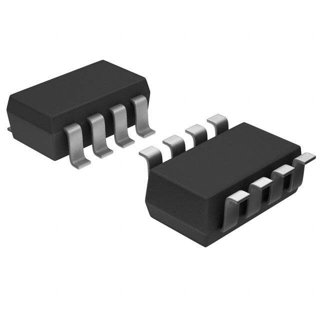
| 描述 | IC OPAMP AUDIO 11MHZ RRO 8VSSOP音频放大器 Sound-Plus High-Perf JFET-In Audio Op Amp |
| 产品分类 | Linear - Amplifiers - Instrumentation, OP Amps, Buffer Amps集成电路 - IC |
| 品牌 | Texas Instruments |
| 产品手册 | http://www.ti.com/litv/sbos484b |
| 产品图片 |
|
| rohs | 符合RoHS无铅 / 符合限制有害物质指令(RoHS)规范要求 |
| 产品系列 | 音频 IC,音频放大器,Texas Instruments OPA1641AIDGKTSoundPlus™ |
| 数据手册 | 点击此处下载产品Datasheethttp://www.ti.com/lit/pdf/slyb174 |
| 产品型号 | OPA1641AIDGKT |
| PCN设计/规格 | |
| THD+噪声 | 0.00005 % |
| 产品 | General Purpose Audio Amplifiers |
| 产品种类 | 音频放大器 |
| 供应商器件封装 | 8-VSSOP |
| 共模抑制比—最小值 | 126 dB |
| 其它名称 | 296-28059-1 |
| 包装 | 剪切带 (CT) |
| 压摆率 | 20 V/µs |
| 商标 | Texas Instruments |
| 增益带宽生成 | 11 MHz |
| 增益带宽积 | 11MHz |
| 安装类型 | 表面贴装 |
| 安装风格 | SMD/SMT |
| 封装 | Reel |
| 封装/外壳 | 8-TSSOP,8-MSOP(0.118",3.00mm 宽) |
| 封装/箱体 | VSSOP-8 |
| 工作温度 | -40°C ~ 85°C |
| 工作电源电压 | 4.5 V to 36 V |
| 工厂包装数量 | 250 |
| 放大器类型 | 音频 |
| 最大工作温度 | + 85 C |
| 最小工作温度 | - 40 C |
| 标准包装 | 1 |
| 电压-电源,单/双 (±) | 4.5 V ~ 36 V, ±2.25 V ~ 18 V |
| 电压-输入失调 | 1mV |
| 电流-电源 | 1.8mA |
| 电流-输入偏置 | 2pA |
| 电流-输出/通道 | 36mA |
| 电源电压-最大 | 18 V |
| 电源电压-最小 | 2.25 V |
| 电源电流 | 1.8 mA |
| 电路数 | 1 |
| 类型 | 1-Channel Rail-to-Rail |
| 系列 | OPA1641 |
| 设计资源 | http://www.digikey.com/product-highlights/cn/zh/texas-instruments-webench-design-center/3176 |
| 输入补偿电压 | 3.5 mV |
| 输出功率 | - |
| 输出类型 | 满摆幅 |


PDF Datasheet 数据手册内容提取
Product Sample & Technical Tools & Support & Reference Folder Buy Documents Software Community Design OPA1641,OPA1642,OPA1644 SBOS484D–DECEMBER2009–REVISEDAPRIL2016 OPA164x SoundPlus™ High-Performance, JFET-Input Audio Operational Amplifiers 1 Features 3 Description • SuperiorSoundQuality The OPA1641 (single), OPA1642 (dual), and 1 OPA1644 (quad) series are JFET-input, ultralow • TrueJFETInputOperationalAmplifier distortion, low-noise operational amplifiers fully WithLowInputBiasCurrent specifiedforaudioapplications. • LowNoise:5.1nV/√Hzat1kHz The OPA1641, OPA1642, and OPA1644 rail-to-rail • UltralowDistortion:0.00005%at1kHz output swing allows increased headroom, making • HighSlewRate:20V/μs these devices ideal for use in any audio circuit. Features include 5.1-nV/√Hz noise, low THD+N • UnityGainStable (0.00005%), a low input bias current of 2 pA, and low • NoPhaseReversal quiescentcurrentof1.8mAperchannel. • LowQuiescentCurrent: These devices operate over a very wide supply 1.8mAperChannel voltage range of ±2.25 V to ±18 V. The OPA1641, • Rail-to-railOutput OPA1642, and OPA1644 series of operational • WideSupplyRange:±2.25Vto ±18V amplifiers are unity-gain stable and provide excellent dynamic behavior over a wide range of load • Single,Dual,andQuadVersionsAvailable conditions. 2 Applications The dual and quad versions feature completely independent circuitry for lowest crosstalk and • ProfessionalAudioEquipment freedom from interactions between channels, even • AnalogandDigitalMixingConsoles whenoverdrivenoroverloaded. • BroadcastStudioEquipment The OPA1641, OPA1642, and OPA1644 are • High-EndA/VReceivers specifiedfrom–40°Cto+85°C. SoundPlus™ • High-EndBlu-ray™Players DeviceInformation(1) PARTNUMBER PACKAGE BODYSIZE(NOM) SOIC(8) 4.90mm×3.90mm OPA1641 VSSOP(8) 3.00mm×3.00mm SOIC(8) 4.90mm×3.90mm OPA1642 VSSOP(8) 3.00mm×3.00mm SOIC(14) 8.65mm×3.90mm OPA1644 TSSOP(14) 5.00mm×4.40mm (1) For all available packages, see the orderable addendum at theendofthedatasheet. space SimplifiedInternalSchematic ExtremelyStableInputCapacitance 7.5 V+ F) 7 p e ( Traditional JFET-Input Amplifier nc6.5 a cit pa 6 OPA164x Family a C Pre-Output Driver OUT de 5.5 o M n- 5 IN- IN+ o m m o4.5 C 4 V- –10 –8 –6 –4 –2 0 2 4 6 8 10 Common-Mode Voltage (V) C004 1 An IMPORTANT NOTICE at the end of this data sheet addresses availability, warranty, changes, use in safety-critical applications, intellectualpropertymattersandotherimportantdisclaimers.PRODUCTIONDATA.
OPA1641,OPA1642,OPA1644 SBOS484D–DECEMBER2009–REVISEDAPRIL2016 www.ti.com Table of Contents 1 Features.................................................................. 1 8 ApplicationandImplementation........................ 18 2 Applications........................................................... 1 8.1 ApplicationInformation............................................18 3 Description............................................................. 1 8.2 TypicalApplication .................................................25 4 RevisionHistory..................................................... 2 9 PowerSupplyRecommendations...................... 27 5 PinConfigurationandFunctions......................... 4 10 Layout................................................................... 28 6 Specifications......................................................... 6 10.1 LayoutGuidelines.................................................28 6.1 AbsoluteMaximumRatings .....................................6 10.2 LayoutExample....................................................29 6.2 ESDRatings ............................................................6 11 DeviceandDocumentationSupport................. 30 6.3 RecommendedOperatingConditions.......................6 11.1 DeviceSupport ....................................................30 6.4 ThermalInformation..................................................6 11.2 DocumentationSupport .......................................30 6.5 ElectricalCharacteristics...........................................7 11.3 RelatedLinks........................................................31 6.6 TypicalCharacteristics..............................................9 11.4 CommunityResources..........................................31 7 DetailedDescription............................................ 14 11.5 Trademarks...........................................................31 7.1 Overview.................................................................14 11.6 ElectrostaticDischargeCaution............................31 7.2 FunctionalBlockDiagram.......................................14 11.7 Glossary................................................................31 7.3 FeatureDescription.................................................15 12 Mechanical,Packaging,andOrderable Information........................................................... 31 7.4 DeviceFunctionalModes........................................17 4 Revision History NOTE:Pagenumbersforpreviousrevisionsmaydifferfrompagenumbersinthecurrentversion. ChangesfromRevisionC(December2015)toRevisionD Page • AddedTIDesign .................................................................................................................................................................... 1 • ChangedMSOPtoVSSOPthroughoutdocument ................................................................................................................ 1 • ChangedSupplyvoltageparameterinRecommendedOperatingConditionstabletosplitsingleanddualsupply specificationsintoseparaterowsforclarity............................................................................................................................ 6 • ChangedlastcolumnheaderinThermalInformationtablefromDGK(VSSOP)toPW(TSSOP)........................................ 6 • ChangedNoisesubsectionofElectricalCharacteristicstable:changedInputvoltagenoiseparametertypical specificationandchangedfirsttwoe parametertypicalspecifications................................................................................. 7 n • ChangedInputBiasCurrentsubsectionofElectricalCharacteristicstable........................................................................... 7 • ChangedV parametertestconditionsinElectricalCharacteristicstable ............................................................................ 8 O • AddedI parameterspecificationstoElectricalCharacteristicstable ................................................................................. 8 SC • ChangedTemperatureRangesubsectionofElectricalCharacteristicstable ....................................................................... 8 • ChangedthirdparagraphofPowerDissipationandThermalProtectionsectionforclarity ................................................ 23 • ChangedsecondparagraphofElectricalOverstresssectionforclarity............................................................................... 23 • AddedtextreferenceforEquation5.................................................................................................................................... 27 ChangesfromRevisionB(August2010)toRevisionC Page • AddedPinConfigurationandFunctionssection,ESDRatingstable,FeatureDescriptionsection,DeviceFunctional Modes,ApplicationandImplementationsection,PowerSupplyRecommendationssection,Layoutsection,Device andDocumentationSupportsection,andMechanical,Packaging,andOrderableInformationsection .............................. 1 • AddedtexttolastbulletofLayoutGuidelinessection.......................................................................................................... 28 ChangesfromRevisionA(April2010)toRevisionB Page • Removedproduct-previewinformationforMSOP-8packageversionofOPA1641............................................................... 1 2 SubmitDocumentationFeedback Copyright©2009–2016,TexasInstrumentsIncorporated ProductFolderLinks:OPA1641 OPA1642 OPA1644
OPA1641,OPA1642,OPA1644 www.ti.com SBOS484D–DECEMBER2009–REVISEDAPRIL2016 ChangesfromOriginal(December2009)toRevisionA Page • Removedproduct-previewinformationforOPA1644devicepackagesthroughoutdocument.............................................. 1 Copyright©2009–2016,TexasInstrumentsIncorporated SubmitDocumentationFeedback 3 ProductFolderLinks:OPA1641 OPA1642 OPA1644
OPA1641,OPA1642,OPA1644 SBOS484D–DECEMBER2009–REVISEDAPRIL2016 www.ti.com 5 Pin Configuration and Functions OPA1641:DandDGKPackages 8-PinSOICandVSSOP TopView (1) (1) NC 1 8 NC -In 2 7 V+ +In 3 6 Out V- 4 5 NC(1) (1) NC denotes no internal connection. PinFunctions:OPA1641 PIN I/O DESCRIPTION NO. NAME 1 NC — Noconnection 2 –IN I Invertinginput 3 +IN I Noninvertinginput 4 V– — Negative(lowest)powersupply 5 NC — Noconnection 6 OUT O Output 7 V+ — Positive(highest)powersupply 8 NC — Noconnection OPA1642:DandDGKPackages 8-PinSOICandVSSOP TopView OUT A 1 8 V+ -In A 2 A 7 Out B +In A 3 B 6 -In B V- 4 5 +In B PinFunctions:OPA1642 PIN I/O DESCRIPTION NO. NAME 1 OUTA O Output,channelA 2 –INA I Invertinginput,channelA 3 +INA I Noninvertinginput,channelA 4 V– — Negative(lowest)powersupply 5 +INB I Noninvertinginput,channelB 6 –INB I Invertinginput,channelB 7 OUTB O Output,channelB 8 V+ — Positive(highest)powersupply 4 SubmitDocumentationFeedback Copyright©2009–2016,TexasInstrumentsIncorporated ProductFolderLinks:OPA1641 OPA1642 OPA1644
OPA1641,OPA1642,OPA1644 www.ti.com SBOS484D–DECEMBER2009–REVISEDAPRIL2016 OPA1644:DandPWPackages 14-PinSOICandTSSOP TopView Out A 1 14 Out D -In A 2 13 -In D A D +In A 3 12 +In D V+ 4 11 V- + In B 5 10 + In C B C -In B 6 9 -In C Out B 7 8 Out C PinFunctions:OPA1644 PIN I/O DESCRIPTION NO. NAME 1 OUTA O Output,channelA 2 –INA I Invertinginput,channelA 3 +INA I Noninvertinginput,channelA 4 V+ — Positive(highest)powersupply 5 +INB I Noninvertinginput,channelB 6 –INB I Invertinginput,channelB 7 OUTB O Output,channelB 8 OUTC O Output,channelC 9 –INC I Invertinginput,channelC 10 +INC I Noninvertinginput,channelC 11 V– — Negative(lowest)powersupply 12 +IND I Noninvertinginput,channelD 13 –IND I Invertinginput,channelD 14 OUTD O Output,channelD Copyright©2009–2016,TexasInstrumentsIncorporated SubmitDocumentationFeedback 5 ProductFolderLinks:OPA1641 OPA1642 OPA1644
OPA1641,OPA1642,OPA1644 SBOS484D–DECEMBER2009–REVISEDAPRIL2016 www.ti.com 6 Specifications 6.1 Absolute Maximum Ratings overoperatingfree-airtemperaturerange(unlessotherwisenoted)(1) MIN MAX UNIT V Supplyvoltage 40 V S V Inputvoltage(2) (V–)–0.5 (V+)+0.5 V IN I Inputcurrent(2) ±10 mA IN V Differentialinputvoltage ±VS V IN(DIFF) I Outputshort-circuit(3) Continuous O T Operatingtemperature –55 125 °C A T Junctiontemperature –65 150 °C J T Storagetemperature –65 150 °C stg (1) StressesbeyondthoselistedunderAbsoluteMaximumRatingsmaycausepermanentdamagetothedevice.Thesearestressratings only,whichdonotimplyfunctionaloperationofthedeviceattheseoranyotherconditionsbeyondthoseindicatedunderRecommended OperatingConditions.Exposuretoabsolute-maximum-ratedconditionsforextendedperiodsmayaffectdevicereliability. (2) Inputpinsarediode-clampedtothepower-supplyrails.Inputsignalsthatcanswingmorethan0.5Vbeyondthesupplyrailsmustbe current-limitedto10mAorless.Theinputvoltageandoutputnegative-voltageratingscanbeexceedediftheinputandoutputcurrent ratingsarefollowed. (3) Short-circuittoV /2(groundinsymmetricaldual-supplysetups),oneamplifierperpackage. S 6.2 ESD Ratings VALUE UNIT Human-bodymodel(HBM),perANSI/ESDA/JEDECJS-001(1) ±3000 V Electrostaticdischarge V (ESD) Charged-devicemodel(CDM),perJEDECspecificationJESD22-C101(2) ±1000 (1) JEDECdocumentJEP155statesthat500-VHBMallowssafemanufacturingwithastandardESDcontrolprocess. (2) JEDECdocumentJEP157statesthat250-VCDMallowssafemanufacturingwithastandardESDcontrolprocess. 6.3 Recommended Operating Conditions overoperatingfree-airtemperaturerange(unlessotherwisenoted) MIN NOM MAX UNIT Singlesupply 4.5 36 Supplyvoltage(V+,V–) V Dualsupply ±2.25 ±18 Specifiedtemperature –40 85 °C 6.4 Thermal Information OPA1641,OPA1642 OPA1644 THERMALMETRIC(1) D(SOIC) DGK(VSSOP) D(SOIC) PW(TSSOP) UNIT 8PINS 8PINS 14PINS 14PINS R Junction-to-ambientthermalresistance 160 180 97 135 °C/W θJA R Junction-to-case(top)thermalresistance 75 55 56 45 °C/W θJC(top) R Junction-to-boardthermalresistance 60 130 53 66 °C/W θJB ψ Junction-to-topcharacterizationparameter 9 n/a 19 n/a °C/W JT ψ Junction-to-boardcharacterizationparameter 50 120 46 60 °C/W JB R Junction-to-case(bottom)thermalresistance n/a n/a n/a n/a °C/W θJC(bot) (1) Formoreinformationabouttraditionalandnewthermalmetrics,seetheSemiconductorandICPackageThermalMetricsapplication report,SPRA953. 6 SubmitDocumentationFeedback Copyright©2009–2016,TexasInstrumentsIncorporated ProductFolderLinks:OPA1641 OPA1642 OPA1644
OPA1641,OPA1642,OPA1644 www.ti.com SBOS484D–DECEMBER2009–REVISEDAPRIL2016 6.5 Electrical Characteristics atT =25°C,V =4.5Vto36(±2.25Vto±18V),R =2kΩconnectedtomidsupply,andV =V =midsupply(unless A S L CM OUT otherwisenoted) PARAMETER TESTCONDITIONS MIN TYP MAX UNIT AUDIOPERFORMANCE 0.00005% THD+N Totalharmonicdistortion+noise G=+1,f=1kHz,V =3V O RMS –126 dB SMPTE/DINtwo-tone,4:1 0.00004% (60Hzand7kHz),G=+1, V =3V –128 dB O RMS DIM30(3-kHzsquarewaveand 0.00008% IMD Intermodulationdistortion 15-kHzsinewave),G=+1, V =3V –122 dB O RMS CCIFtwin-tone 0.00007% (19kHzand20kHz),G=+1, V =3V –123 dB O RMS FREQUENCYRESPONSE GBW Gain-bandwidthproduct G=1 11 MHz SR Slewrate G=1 20 V/μs Full-powerbandwidth(1) V =1V 3.2 MHz O P Overloadrecoverytime(2) G=–10 600 ns Channelseparation(dualandquad) f=1kHz –126 dB NOISE Inputvoltagenoise f=20Hzto20kHz 4.3 μV PP f=10Hz 8 e Inputvoltagenoisedensity f=100Hz 5.8 nV/√Hz n f=1kHz 5.1 I Inputcurrentnoisedensity f=1kHz 0.8 fA/√Hz n OFFSETVOLTAGE V Inputoffsetvoltage V =±18V 1 3.5 mV OS S PSRR V vspowersupply V =±2.25Vto±18V 0.14 2 μV/V OS S INPUTBIASCURRENT I Inputbiascurrent V =0V ±2 ±20 pA B CM I Inputoffsetcurrent V =0V ±2 ±20 pA OS CM INPUTVOLTAGERANGE V Common-modevoltagerange (V–)–0.1 (V+)–3.5 V CM V =(V–)–0.1Vto(V+)–3.5V, CMRR Common-moderejectionratio CM 120 126 dB V =±18V S INPUTIMPEDANCE Differential 1013||8 Ω||pF Common-mode V =(V–)–0.1Vto(V+)–3.5V 1013||6 Ω||pF CM OPEN-LOOPGAIN (V–)+0.2V≤V ≤(V+)–0.2V, O 120 134 R =10kΩ L A Open-loopvoltagegain dB OL (V–)+0.35V≤V ≤(V+)–0.35V, O 114 126 R =2kΩ L (1) Fullpowerbandwidth=SR/(2π×V ),whereSR=slewrate. P (2) SeeFigure19andFigure20. Copyright©2009–2016,TexasInstrumentsIncorporated SubmitDocumentationFeedback 7 ProductFolderLinks:OPA1641 OPA1642 OPA1644
OPA1641,OPA1642,OPA1644 SBOS484D–DECEMBER2009–REVISEDAPRIL2016 www.ti.com Electrical Characteristics (continued) atT =25°C,V =4.5Vto36(±2.25Vto±18V),R =2kΩconnectedtomidsupply,andV =V =midsupply(unless A S L CM OUT otherwisenoted) PARAMETER TESTCONDITIONS MIN TYP MAX UNIT OUTPUT R =10kΩ,A ≥120dB (V–)+0.2 (V+)–0.2 L OL V Voltageoutputswingfromrail V O R =2kΩ,A ≥114dB (V–)+0.35 (V+)–0.35 L OL I Outputcurrent SeeTypicalCharacteristics OUT Z Open-loopoutputimpedance SeeTypicalCharacteristics O Source 36 I Short-circuitcurrent mA SC Sink –30 C Capacitiveloaddrive SeeTypicalCharacteristics LOAD POWERSUPPLY V Specifiedvoltage ±2.25 ±18 V S I Quiescentcurrent(peramplifier) I =0A 1.8 2.3 mA Q OUT TEMPERATURERANGE Specifiedrange –40 85 °C Operatingrange –55 125 °C 8-pinSOICpackage 138 8-pinVSSOPpackage 180 Thermalresistance °C/W 14-pinSOICpackage 97 14-pinTSSOPpackage 135 8 SubmitDocumentationFeedback Copyright©2009–2016,TexasInstrumentsIncorporated ProductFolderLinks:OPA1641 OPA1642 OPA1644
OPA1641,OPA1642,OPA1644 www.ti.com SBOS484D–DECEMBER2009–REVISEDAPRIL2016 6.6 Typical Characteristics atT =25°C,R =2kΩconnectedtomidsupply,andV =V =midsupply(unlessotherwisenoted) A L CM OUT 100 )z H Ö V/ n y ( Densit 10 V/div Noise 100n e g a olt V 1 0.1 1 10 100 1k 10k 100k Frequency (Hz) Time (1s/div) Figure1.InputVoltageNoiseDensityvsFrequency Figure2.0.1-Hzto10-HzNoise 35 160 Output Voltage (V)PP 3221105050 VVSS==±±155VV Mvwinoidatlhtuxaoicmgueetud smr dale insowgtuo-etrrpatiutoetn n-Mode Rejection Ratio (dB)Supply Rejection Ratio (dB) 111420864000000 +PSRR -CPSMRRRR 5 VS=±2.25V CommoPower- 20 0 0 10k 100k 1M 10M 1 10 100 1k 10k 100k 1M 10M 100M Frequency (Hz) Frequency (Hz) Figure3.MaximumOutputVoltagevsFrequency Figure4.CMRRandPSRRvsFrequency (ReferredtoInput) 140 180 30 120 Gain 20 100 135 G = +10 P B) 80 has B) 10 Gain (d 6400 90 e (degre Gain (d 0 G = +1 e Phase s ) 20 45 -10 0 G =-1 -20 0 -20 50100 1k 10k 100k 1M 10M 100M 100k 1M 10M 100M Frequency (Hz) Frequency (Hz) Figure5.GainandPhasevsFrequency Figure6.Closed-LoopGainvsFrequency Copyright©2009–2016,TexasInstrumentsIncorporated SubmitDocumentationFeedback 9 ProductFolderLinks:OPA1641 OPA1642 OPA1644
OPA1641,OPA1642,OPA1644 SBOS484D–DECEMBER2009–REVISEDAPRIL2016 www.ti.com Typical Characteristics (continued) atT =25°C,R =2kΩconnectedtomidsupply,andV =V =midsupply(unlessotherwisenoted) A L CM OUT 0.001 -100 0.01 -80 Total Harmonic Distortion + Noise (%) 0.0001 VBWOU T== GR8 03L =kV=HR- 6Mz10S0W GRL == + 6100WGRL ==GR- 2L1 =k=W + 21kW -120 Total Harmonic Distortion + Noise (dB Total Harmonic Distortion + Noise (%) 0.00.000011 VBWOU T>= 5 030VkRHMzS GRL == + 610GR0WL == + 2GR1kL W==- 21kW GRL ==- 6100W --110200 Total Harmonic Distortion + Noise (dB 0.00001 -140 ) 0.00001 -140 ) 10 100 1k 10k 20k 10 100 1k 10k 100k Frequency (Hz) Frequency (Hz) Figure7.THD+NRatiovsFrequency Figure8.THD+NRatiovsFrequency 0.01 -80 0.01 -80 %) BW = 80kHz To G = +1 Total Harmonic Distortion + Noise ( 0.00.000.000000111 R1kSHOUzR SGGCiE g==n= -+a 011lW,,RRLL== 22kkWW ---111024000 tal Harmonic Distortion + Noise (dB) Intermodulation Distortion (%) 0.00.000.000000111 C(1C9IkFHST4 Tzw:Mw1 ao Pi(nn-6TTd-o0TE on2H/ne0Dzek IaHNnzd) 7kHD(a3znIkM)dH 31z05 skqHuza rsein we awvaeve) ---111024000 Intermodulation Distortion (dB) 0.1 1 10 20 0.1 1 10 20 Output Amplitude (V ) Output Amplitude (V ) RMS RMS Figure9.THD+NRatiovsOutputAmplitude Figure10. IntermodulationDistortion vsOutputAmplitude -80 V =±15V S V = 3V -90 OUT RMS B) G = +1 Output d n ( -100 atio RL= 600W Separ -110 V/div annel -120 RL= 2kW 5 +18V Ch OPA1641 -130 Output RL= 5kW 37V-PP18V -140 Sine Wave (±18.5V) 10 100 1k 10k 100k Frequency (Hz) Time (0.4ms/div) Figure11. ChannelSeparationvsFrequency Figure12.NoPhaseReversal 10 SubmitDocumentationFeedback Copyright©2009–2016,TexasInstrumentsIncorporated ProductFolderLinks:OPA1641 OPA1642 OPA1644
OPA1641,OPA1642,OPA1644 www.ti.com SBOS484D–DECEMBER2009–REVISEDAPRIL2016 Typical Characteristics (continued) atT =25°C,R =2kΩconnectedtomidsupply,andV =V =midsupply(unlessotherwisenoted) A L CM OUT G = +1 G =-1 C = 100pF C = 100pF L L v v V/di +15V V/di RI=2kW RF=2kW m m 20 OPA1641 20 +15V -15V RL CL OPA1641 -15V CL Time (100ns/div) Time (100ns/div) Figure13. Small-SignalStepResponse(100mV) Figure14. Small-SignalStepResponse(100mV) G = +1 G =-1 C = 100pF C = 100pF L L v v di di V/ V/ 2 2 Time (400ns/div) Time (400ns/div) Figure15. Large-SignalStepResponse Figure16. Large-SignalStepResponse VOUT G =-10 G =-10 V IN v v di di V/ V/ 5 20kW 5 20kW V 2kW 2kW IN VIN OPA1641 VOUT VIN OPA1641 VOUT V OUT Time (0.4ms/div) Time (0.4ms/div) Figure17.PositiveOverloadRecovery Figure18.NegativeOverloadRecovery Copyright©2009–2016,TexasInstrumentsIncorporated SubmitDocumentationFeedback 11 ProductFolderLinks:OPA1641 OPA1642 OPA1644
OPA1641,OPA1642,OPA1644 SBOS484D–DECEMBER2009–REVISEDAPRIL2016 www.ti.com Typical Characteristics (continued) atT =25°C,R =2kΩconnectedtomidsupply,andV =V =midsupply(unlessotherwisenoted) A L CM OUT 40 45 %) 332505 G = +1 ROUT= 0W OP+-A111556VV41 ROUT RL CL %) 433050 RI=2kW ORPF+-A=111 2556kVV4W1 ROUT CL RORUOTU=T 2=4 0WW hoot ( 20 ROUT= 24W hoot ( 25 s s 20 er er Ov 15 R = 51W Ov 15 ROUT= 51W OUT 10 10 5 5 G =-1 0 0 0 100 200 300 400 500 600 700 800 900 1000 0 100 200 300 400 500 600 700 800 900 1000 Capacitive Load (pF) Capacitive Load (pF) Figure19. Small-SignalOvershootvsCapacitiveLoad Figure20. Small-SignalOvershootvsCapacitiveLoad (100-mVOutputStep) (100-mVOutputStep) 0 80 70 -0.2 10kW 60 +I B 50 -0.4 A) V/V) (pS 40 A(mOL --00..68 2kW Iand IBO 321000 -IB 0 -1.0 -10 -I OS -1.2 -20 -40 -15 10 35 60 85 -40 -15 10 35 60 85 Temperature (°C) Temperature (°C) Figure21.Open-LoopGainvsTemperature Figure22. IBandIOSvsTemperature 10 2.5 V =±18V S 8 6 2.0 +I A) 4 B -IB p 2 1.5 (S A) and IO -02 IOS I(mQ 1.0 B I -4 -6 0.5 -8 Common-Mode Range -10 0 -18 -12 -6 0 6 12 18 -40 -25 -10 5 20 35 50 65 80 95 110 125 Common-Mode Voltage (V) Temperature (°C) Figure23. IBandIOSvsCommon-ModeVoltage Figure24. QuiescentCurrentvsTemperature 12 SubmitDocumentationFeedback Copyright©2009–2016,TexasInstrumentsIncorporated ProductFolderLinks:OPA1641 OPA1642 OPA1644
OPA1641,OPA1642,OPA1644 www.ti.com SBOS484D–DECEMBER2009–REVISEDAPRIL2016 Typical Characteristics (continued) atT =25°C,R =2kΩconnectedtomidsupply,andV =V =midsupply(unlessotherwisenoted) A L CM OUT 2.00 60 1.75 50 1.50 I SC-SOURCE 40 1.25 A) A) (m 1.00 (m 30 IQ 0.75 ISC ISC-SINK 20 0.50 10 V = Midsupply 0.25 Specified Supply-Voltage Range OUT (includes self-heating) 0 0 0 4 8 12 16 20 24 28 32 36 -50 -25 0 25 50 75 100 125 Supply Voltage (V) Temperature (°C) Figure25. QuiescentCurrentvsSupplyVoltage Figure26. Short-CircuitCurrentvsTemperature 18.0 1k 17.5 17.0 e (V) 1166..50 100 Voltag -40°C +25°C+85°C +125°C W()O put -16.0 Z ut 10 O -16.5 -17.0 -17.5 -18.0 1 0 10 20 30 40 50 10 100 1k 10k 100k 1M 10M 100M Output Current (mA) Frequency (Hz) Figure27.OutputVoltagevsOutputCurrent Figure28. Open-LoopOutputImpedancevsFrequency Copyright©2009–2016,TexasInstrumentsIncorporated SubmitDocumentationFeedback 13 ProductFolderLinks:OPA1641 OPA1642 OPA1644
OPA1641,OPA1642,OPA1644 SBOS484D–DECEMBER2009–REVISEDAPRIL2016 www.ti.com 7 Detailed Description 7.1 Overview The OPA164x family of operational amplifiers combine an ultra low noise JFET input stage with a rail-to-rail output stage to provide high overall performance in audio applications. The internal topology is selected specifically to deliver extremely low distortion, consume limited power, and accommodate small packages. These amplifiers are well-suited for analog signal processing applications such as active filter circuits, pre-amplifiers, and tone controls. The unique input stage design and semiconductor processes used in this device deliver extremely high performance even in applications with high source impedance and wide common-mode voltage swings. 7.2 Functional Block Diagram V+ Pre-Output Driver OUT IN- IN+ V- 14 SubmitDocumentationFeedback Copyright©2009–2016,TexasInstrumentsIncorporated ProductFolderLinks:OPA1641 OPA1642 OPA1644
OPA1641,OPA1642,OPA1644 www.ti.com SBOS484D–DECEMBER2009–REVISEDAPRIL2016 7.3 Feature Description 7.3.1 PhaseReversalProtection The OPA164x family has internal phase-reversal protection. Many op amps exhibit phase reversal when the input is driven beyond the linear common-mode range. This condition is most often encountered in noninverting circuits when the input is driven beyond the specified common-mode voltage range, causing the output to reverse into the opposite rail. The input of the OPA164x prevents phase reversal with excessive common-mode voltage.Instead,theappropriateraillimitstheoutputvoltage.ThisperformanceisshowninFigure29. Output v di V/ 5 +18V OPA1641 Output -18V 37VPP Sine Wave (±18.5V) Time (0.4ms/div) Figure29. OutputWaveformDevoidofPhaseReversalDuringanInputOverdriveCondition 7.3.2 OutputCurrentLimit The output current of the OPA164x series is limited by internal circuitry to 36 mA and –30 mA (sourcing and sinking), to protect the device if the output is accidentally shorted. This short-circuit current depends on temperature;seeFigure26. Although uncommon for most modern audio applications to require 600-Ω load drive capability, many audio operational amplifier applications continue to specify the total harmonic distortion (THD+N) at 600-Ω load for comparative purposes. Figure 7 and Figure 8 provide typical THD+N measurement curves for the OPA164x series, where the output drives a 3-V signal into a 600-Ω load. However, correct device operation cannot be RMS ensured when driving 600-Ω loads at full supply. Depending on supply voltage and temperature, this operating conditioncanpossiblytriggertheoutputcurrentlimitcircuitryofthedevice. 7.3.3 EMIRejectionRatio(EMIRR) The electromagnetic interference (EMI) rejection ratio, or EMIRR, describes the EMI immunity of operational amplifiers.Anadverseeffectthatiscommontomanyoperationalamplifiersisachangeintheoffsetvoltageasa result of RF signal rectification. An operational amplifier that is more efficient at rejecting this change in offset as a result of EMI has a higher EMIRR and is quantified by a decibel value. Measuring EMIRR can be performed in many ways, but this document provides the EMIRR IN+, which specifically describes the EMIRR performance when the RF signal is applied to the noninverting input pin of the operational amplifier. In general, only the noninvertinginputistestedforEMIRRforthefollowingthreereasons: • Operational amplifier input pins are known to be the most sensitive to EMI, and typically rectify RF signals betterthanthesupplyoroutputpins. • The noninverting and inverting operational amplifier inputs have symmetrical physical layouts and exhibit nearlymatchingEMIRRperformance. • EMIRR is easier to measure on noninverting pins than on other pins because the noninverting input pin can be isolated on a printed-circuit-board (PCB). This isolation allows the RF signal to be applied directly to the noninvertinginputpinwithnocomplexinteractionsfromothercomponentsorconnectingPCBtraces. A more formal discussion of the EMIRR IN+ definition and test method is provided in application report EMI RejectionRatioofOperationalAmplifiers (SBOA128),availablefordownloadatwww.ti.com. Copyright©2009–2016,TexasInstrumentsIncorporated SubmitDocumentationFeedback 15 ProductFolderLinks:OPA1641 OPA1642 OPA1644
OPA1641,OPA1642,OPA1644 SBOS484D–DECEMBER2009–REVISEDAPRIL2016 www.ti.com Feature Description (continued) The EMIRR IN+ of the OPA164x is plotted versus frequency in Figure 30. If available, any dual and quad operational amplifier device versions have nearly identical EMIRR IN+ performance. The OPA164x unity-gain bandwidth is 11 MHz. EMIRR performance below this frequency denotes interfering signals that fall within the operationalamplifierbandwidth. 140 120 100 B) d 80 R ( R MI 60 E 40 20 0 10M 100M 1G 10G Frequency (Hz) C003 Figure30. OPA164xEMIRRvsFrequency Table 1 lists the EMIRR IN+ values for the OPA164x at particular frequencies commonly encountered in real- world applications. Applications listed in Table 1 can be centered on or operated near the particular frequency shown. This information can be of special interest to designers working with these types of applications, or working in other fields likely to encounter RF interference from broad sources, such as the industrial, scientific, andmedical(ISM)radioband. Table1.OPA164xEMIRRIN+forFrequenciesofInterest FREQUENCY APPLICATION,ALLOCATION EMIRRIN+ 400MHz Mobileradio,mobilesatellite,spaceoperation,weather,radar,UHF 53.1dB GSM,radiocommunicationandnavigation,GPS(to1.6GHz),ISM, 900MHz 72.2dB aeronauticalmobile,UHF 1.8GHz GSM,mobilepersonalcomm.broadband,satellite,L-band 80.7dB 2.4GHz 802.11b/g/n,Bluetooth™,mobilepersonalcomm.,ISM,amateurradioandsatellite,S-band 86.8dB 3.6GHz Radiolocation,aerocomm./nav.,satellite,mobile,S-band 91.7dB 802.11a/n,aerocommunicationandnavigation,mobilecommunication, 5GHz 96.6dB spaceandsatelliteoperation,C-band 16 SubmitDocumentationFeedback Copyright©2009–2016,TexasInstrumentsIncorporated ProductFolderLinks:OPA1641 OPA1642 OPA1644
OPA1641,OPA1642,OPA1644 www.ti.com SBOS484D–DECEMBER2009–REVISEDAPRIL2016 7.3.3.1 EMIRRIN+TestConfiguration Figure 31 shows the circuit configuration for testing the EMIRR IN+. An RF source is connected to the operational amplifier noninverting input pin using a transmission line. The operational amplifier is configured in a unity-gain buffer topology with the output connected to a low-pass filter (LPF) and a digital multimeter (DMM). A large impedance mismatch at the operational amplifier input causes a voltage reflection; however, this effect is characterized and accounted for when determining the EMIRR IN+. The resulting dc offset voltage is sampled andmeasuredbythemultimeter.TheLPFisolatesthemultimeterfromresidualRFsignalsthatcaninterferewith multimeteraccuracy.SeeEMIRejectionRatioofOperationalAmplifiers (SBOA128)formoredetails. Ambient temperature: 25(cid:219)& +VS – 50 (cid:13)(cid:3) Low-Pass Filter + RF source DC Bias: 0 V -VS Sample / Modulation: None (CW) Digital Multimeter Frequency Sweep: 201 pt. Log Not shown: 0.1 µF and 10 µF Averaging supply decoupling Figure31. EMIRRIN+TestConfigurationSchematic 7.4 Device Functional Modes 7.4.1 OperatingVoltage The OPA1641, OPA1642, and OPA1644 series of operational amplifiers can be used with single or dual supplies from an operating range of V = 4.5 V (±2.25 V) and up to V = 36 V (±18 V). These devices do not require S S symmetrical supplies; only a minimum supply voltage of 4.5 V (±2.25 V) is required. For V less than ±3.5 V, the S common-mode input range does not include midsupply. Supply voltages higher than 40 V can permanently damagethedevice;seetheAbsoluteMaximumRatingstableformoreinformation.Keyparametersarespecified over the operating temperature range, T = –40°C to +85°C. Key parameters that vary over the supply voltage or A temperaturerangeareillustratedintheTypicalCharacteristicssection. Copyright©2009–2016,TexasInstrumentsIncorporated SubmitDocumentationFeedback 17 ProductFolderLinks:OPA1641 OPA1642 OPA1644
OPA1641,OPA1642,OPA1644 SBOS484D–DECEMBER2009–REVISEDAPRIL2016 www.ti.com 8 Application and Implementation NOTE Information in the following applications sections is not part of the TI component specification, and TI does not warrant its accuracy or completeness. TI’s customers are responsible for determining suitability of components for their purposes. Customers should validateandtesttheirdesignimplementationtoconfirmsystemfunctionality. 8.1 Application Information The OPA1641, OPA1642, and OPA1644 are unity-gain stable, audio operational amplifiers with very low noise, input bias current, and input offset voltage. Applications with noisy or high-impedance power supplies require decoupling capacitors placed close to the device pins. In most cases, 0.1-μF capacitors are adequate. Figure 32 showsasimplifiedschematicoftheOPA1641. V+ Pre-Output Driver OUT IN- IN+ V- Figure32. SimplifiedInternalSchematic 8.1.1 NoisePerformance Figure 33 illustrates the total circuit noise for varying source impedances with the operational amplifier in a unity- gain configuration (with no feedback resistor network and therefore no additional noise contributions). The OPA1641, OPA1642, and OPA1644 are shown with total circuit noise calculated. The operational amplifier contributes both a voltage noise component and a current noise component. The voltage noise is commonly modeled as a time-varying component of the offset voltage. The current noise is modeled as the time-varying component of the input bias current and reacts with the source resistance to create a voltage component of noise. Therefore, the lowest noise operational amplifier for a given application depends on the source impedance. For low source impedance, current noise is negligible, and voltage noise generally dominates. The OPA1641, OPA1642, and OPA1644 family has both low voltage noise and extremely low current noise because of the FET input of the operational amplifier. As a result, the current noise contribution of the OPA164x series is negligible for any practical source impedance, which makes the OPA164x series of amplifiers better choices for applicationswithhighsourceimpedance. TheequationinFigure33illustratesthecalculationofthetotalcircuitnoise,where: • e =voltagenoise n • I =currentnoise n • R =sourceimpedance S • k=Boltzmann'sconstant=1.38× 10⁻²³J/K • T=temperatureindegreesKelvin(K) Formoredetailsoncalculatingnoise,seetheBasicNoiseCalculationssection. 18 SubmitDocumentationFeedback Copyright©2009–2016,TexasInstrumentsIncorporated ProductFolderLinks:OPA1641 OPA1642 OPA1644
OPA1641,OPA1642,OPA1644 www.ti.com SBOS484D–DECEMBER2009–REVISEDAPRIL2016 Application Information (continued) 10k O E nsity, 1k EO OPA1611 De RS al ctr pe 100 S e s oi OPA1641 N Resistor Noise e 10 g a otl V 2 2 2 E = e + (i R ) + 4kTR O n n S S 1 100 1k 10k 100k 1M Source Resistance, R (W) S Figure33. NoisePerformanceoftheOPA1611andOPA1641inaUnity-GainBufferConfiguration 8.1.2 BasicNoiseCalculations Low-noise circuit design requires careful analysis of all noise sources. External noise sources can dominate in many cases; consider the effect of source resistance on overall operational amplifier noise performance. Total noiseofthecircuitistheroot-sum-squarecombinationofallnoisecomponents. The resistive portion of the source impedance produces thermal noise proportional to the square root of the resistance. This function is plotted in Figure 33. The source impedance is usually fixed; consequently, select the operationalamplifierandthefeedbackresistorstominimizetherespectivecontributionstothetotalnoise. Figure 34 illustrates both noninverting (A) and inverting (B) operational amplifier circuit configurations with gain. In circuit configurations with gain, the feedback network resistors also contribute noise. In general, the current noise of the operational amplifier reacts with the feedback resistors to create additional noise components. However, the extremely low current noise of the OPA164x means that the device current noise contribution can beneglected. The feedback resistor values can generally be chosen to make these noise sources negligible. Note that low impedance feedback resistors do load the output of the amplifier. The equations for total noise are given in Figure34forbothconfigurations. Copyright©2009–2016,TexasInstrumentsIncorporated SubmitDocumentationFeedback 19 ProductFolderLinks:OPA1641 OPA1642 OPA1644
OPA1641,OPA1642,OPA1644 SBOS484D–DECEMBER2009–REVISEDAPRIL2016 www.ti.com A) Noise in Noninverting Gain Configuration Noise at the output: R 2 2 2 2 R R R R E 2= 1 + 2 e 2+ 2 e 2+ e 2+ 1 + 2 e2 1 O R n R 1 2 R s 1 1 1 E O Where e = 4kTR = thermal noise of R R S S S S e = 4kTR = thermal noise of R 1 1 1 V S e = 4kTR = thermal noise of R 2 2 2 B) Noise in Inverting Gain Configuration Noise at the output: R2 2 2 2 R R R E 2= 1 + 2 e 2+ 2 e 2+ e 2+ 2 e2 R1 O R1+ RS n R1+ RS 1 2 R1+ RS s E R O S Where e = 4kTR = thermal noise of R S S S V S e = 4kTR = thermal noise of R 1 1 1 e = 4kTR = thermal noise of R 2 2 2 For the OPA164x series op amps at 1kHz, e = 5.1nV/ÖHz n Figure34. NoiseCalculationinGainConfigurations 20 SubmitDocumentationFeedback Copyright©2009–2016,TexasInstrumentsIncorporated ProductFolderLinks:OPA1641 OPA1642 OPA1644
OPA1641,OPA1642,OPA1644 www.ti.com SBOS484D–DECEMBER2009–REVISEDAPRIL2016 8.1.3 TotalHarmonicDistortionMeasurements The OPA164x series operational amplifiers have excellent distortion characteristics. THD + noise is below 0.00005% (G = 1, V = 3 V , BW = 80 kHz) throughout the audio frequency range, 20 Hz to 20 kHz, with a O RMS 2-kΩ load(seeFigure7). The distortion produced by the OPA164x series operational amplifiers is below the measurement limit of many commercially available distortion analyzers. However, a special test circuit (such as shown in Figure 35) can be usedtoextendthemeasurementcapabilities. Operational amplifier distortion can be considered an internal error source that can be referred to the input. Figure 35 shows a circuit that causes the operational amplifier distortion to be 101 times (or approximately 40 dB) greater than that normally produced by the operational amplifier. The addition of R to the otherwise 3 standard noninverting amplifier configuration alters the feedback factor or noise gain of the circuit. The closed- loop gain is unchanged, but the feedback available for error correction is reduced by a factor of 101, thus extending the resolution by 101. Note that the input signal and load applied to the operational amplifier are the same as with conventional feedback without R . Keep the value of R small to minimize any effect on distortion 3 3 measurements. The validity of this technique can be verified by duplicating measurements at high gain or high frequency where the distortion is within the measurement capability of the test equipment. Measurements for this document were made with an audio precision system two distortion and noise analyzer that greatly simplifies such repetitive measurements. The measurement technique can, however, be performed with manual distortion measurement instruments. space R R 1 2 SIGNAL DISTORTION GAIN GAIN R1 R2 R3 1 101 ¥ 1kW 10W R R3 OPA1641 VO= 3VRMS 11 101 100W 1kW 11W Signal Gain = 1+ 2 R 1 R Distortion Gain = 1+ 2 R II R 1 3 Generator Analyzer Output Input Audio Precision System Two(1) Load with PC Controller (1) Formeasurementbandwidth,seeFigure7throughFigure10. Figure35. DistortionTestCircuit 8.1.4 SourceImpedanceandDistortion In traditional JFET-input operational amplifiers, the impedance applied to the positive and negative inputs in noninverting applications must be matched for lowest distortion. Legacy methods for fabricating the JFETs in the FET input stage exhibit a varying input capacitance with applied common-mode input voltage. In inverting configurations, the input does not vary with input voltage because the inverting input is held at virtual ground. However, in noninverting applications, the inputs do vary, and the gate-to-source voltage is not constant. This effect produces increased distortion as a result of the varying capacitance for unmatched source impedances. However, the OPA164x family of amplifiers is designed to maintain a constant input capacitance with varying common-mode voltage to prevent this mechanism of distortion. The variation of input capacitance with common- modevoltageforatraditionalamplifieriscomparedtotheOPA164xfamilyinFigure36. Copyright©2009–2016,TexasInstrumentsIncorporated SubmitDocumentationFeedback 21 ProductFolderLinks:OPA1641 OPA1642 OPA1644
OPA1641,OPA1642,OPA1644 SBOS484D–DECEMBER2009–REVISEDAPRIL2016 www.ti.com 7.5 F) 7 p e ( Traditional JFET-Input Amplifier nc6.5 a cit pa 6 OPA164x Family a C de 5.5 o M n- 5 o m m o4.5 C 4 –10 –8 –6 –4 –2 0 2 4 6 8 10 Common-Mode Voltage (V) C004 Figure36. InputCapacitanceoftheOPA164xFamilyofAmplifiersComparedtoTraditionalJFET-input Amplifiers By stabilizing the input capacitance, the distortion performance of the amplifier is greatly improved for noninverting configurations with high source impedances. The measured performance of an OPA164x amplifier is compared to a traditional JFET-input amplifier in Figure 37. The unity-gain configuration, high source impedance,andlarge-signalamplitudeproduceadditionaldistortioninthetraditionalamplifier. 1 -40 Noise (%) 0.1 5 VRMS 10 k(cid:13) +– --6500 Noise (dB) Distortion + 0.01 Traditional JFET-Input Amplifier --8700 Distortion + Harmonic 0.001 OPA164x Amplifier --19000 Harmonic Total 0.0001 --112100 Total 10 100 1000 10000 Frequency (Hz) C005 Figure37. MeasuredTHD+NoftheOPA164xFamilyofAmplifiersComparedtoTraditionalJFET-input Amplifiers 8.1.5 CapacitiveLoadandStability The dynamic characteristics of the OPA164x are optimized for commonly encountered gains, loads, and operating conditions. The combination of low closed-loop gain and high capacitive loads decreases the phase margin of the amplifier and can lead to gain peaking or oscillations. As a result, heavier capacitive loads must be isolatedfromtheoutput.Thesimplestwaytoachievethisisolationistoaddasmallresistor(R equalto50Ω, OUT forexample)inserieswiththeoutput. Figure 19 and Figure 20 illustrate graphs of Small-Signal Overshoot vs Capacitive Load for several values of R . Also, see Applications Bulletin AB-028, Feedback Plots Define Op Amp AC Performance (SBOA015) OUT availablefordownloadatwww.ti.comfordetailsofanalysistechniquesandapplicationcircuits. 8.1.6 PowerDissipationandThermalProtection The OPA164x series of operational amplifiers are capable of driving 2-kΩ loads with power-supply voltages of up to ±18 V over the specified temperature range. In a single-supply configuration, where the load is connected to the negative supply voltage, the minimum load resistance is 2.8 kΩ at a supply voltage of 36 V. For lower supply voltages (either single-supply or symmetrical supplies), a lower load resistance can be used, as long as the outputcurrentdoesnotexceed13mA;otherwise,thedeviceshort-circuitcurrentprotectioncircuitcanactivate. 22 SubmitDocumentationFeedback Copyright©2009–2016,TexasInstrumentsIncorporated ProductFolderLinks:OPA1641 OPA1642 OPA1644
OPA1641,OPA1642,OPA1644 www.ti.com SBOS484D–DECEMBER2009–REVISEDAPRIL2016 Internal power dissipation increases when operating at high supply voltages. Copper leadframe construction used in the OPA1641, OPA1642, and OPA1644 series of devices improves heat dissipation compared to conventional materials. PCB layout can also help reduce a possible increase in junction temperature. Wide copper traces help dissipate the heat by functioning as an additional heatsink. Temperature rise can be further minimizedbysolderingthedevicesdirectlytothePCBratherthanusingasocket. Although the output current is limited by internal protection circuitry, accidental shorting one or more output channels of a device can result in excessive heating. For instance, when an output is shorted to mid-supply, the typical short-circuit current of 36 mA leads to an internal power dissipation of over 600 mW at a supply of ±18 V. In case of a dual OPA1642 in an VSSOP-8 package (thermal resistance θ = 180°C/W), such a power JA dissipation results in the die temperature to be 220°C above ambient temperature, when both channels are shorted.Thistemperatureincreasewilldestroythedevice. To prevent such excessive heating that can destroy the device, the OPA164x series has an internal thermal shutdown circuit that shuts down the device if the die temperature exceeds approximately 180°C. When this thermal shutdown circuit activates, a built-in hysteresis of 15°C ensures that the die temperature must drop to approximately165°Cbeforethedeviceswitchesonagain. 8.1.7 ElectricalOverstress Designers often ask questions about the capability of an operational amplifier to withstand electrical overstress. These questions tend to focus on the device inputs, but can involve the supply voltage pins or even the output pin. Each of these different pin functions have electrical stress limits determined by the voltage breakdown characteristics of the particular semiconductor fabrication process and specific circuits connected to the pin. Additionally, internal electrostatic discharge (ESD) protection is built into these circuits to protect them from accidentalESDeventsbothbeforeandduringproductassembly. Having a good understanding of this basic ESD circuitry and its relevance to an electrical overstress event is helpful. Figure 38 illustrates the ESD circuits contained in the OPA164x series (indicated by the dashed line area). The ESD protection circuitry involves several current-steering diodes connected from the input and output pins and routed back to the internal power-supply lines where an internal absorption device is connected. This protectioncircuitryisintendedtoremaininactiveduringnormalcircuitoperation. An ESD event produces a short duration, high-voltage pulse that is transformed into a short-duration, high- current pulse when discharging through a semiconductor device. The ESD protection circuits are designed to provide a current path around the operational amplifier core to prevent damage. The energy absorbed by the protectioncircuitryisthendissipatedasheat. When an ESD voltage develops across two or more of the amplifier device pins, current flows through one or more of the steering diodes. Depending on the path that the current takes, the absorption device can activate. The absorption device has a trigger, or threshold voltage, that is above the normal operating voltage of the OPA164x but below the device breakdown voltage level. When this threshold is exceeded, the absorption device quicklyactivatesandclampsthevoltageacrossthesupplyrailstoasafelevel. WhentheoperationalamplifierconnectsintoacircuitsuchastheoneillustratedinFigure38,theESDprotection components are intended to remain inactive and not become involved in the application circuit operation. However, circumstances can arise where an applied voltage exceeds the operating voltage range of a given pin. If this condition occurs, some of the internal ESD protection circuits can be biased on and conduct current. Any suchcurrentflowoccursthroughsteeringdiodepathsandrarelyinvolvestheabsorptiondevice. Figure 38 depicts a specific example where the input voltage, V , exceeds the positive supply voltage (+V ) by IN S 500 mV or more. Much of what happens in the circuit depends on the supply characteristics. If +V can sink the S current, one of the upper input steering diodes conducts and directs current to +V . Excessively high current S levelscanflowwithincreasinglyhigherV .Asaresult,thedatasheetspecificationsrecommendthatapplications IN limittheinputcurrentto10mA. If the supply is not capable of sinking the current, V can begin sourcing current to the operational amplifier, and IN then take over as the source of positive supply voltage. The danger in this case is that the voltage can rise to levelsthatexceedtheoperationalamplifierabsolutemaximumratings. Copyright©2009–2016,TexasInstrumentsIncorporated SubmitDocumentationFeedback 23 ProductFolderLinks:OPA1641 OPA1642 OPA1644
OPA1641,OPA1642,OPA1644 SBOS484D–DECEMBER2009–REVISEDAPRIL2016 www.ti.com Another common question involves what happens to the amplifier if an input signal is applied to the input when the power supplies +V and –V are at 0 V. The amplifier behavior depends on the supply characteristic when at S S 0V,oratalevelbelowtheinputsignalamplitude.Ifthesuppliesappearashighimpedance,thentheoperational amplifier supply current can be supplied by the input source through the current steering diodes. This state is not a normal bias condition; the amplifier most likely will not operate normally. If the supplies are low impedance, then the current through the steering diodes can become quite high. The current level depends on the ability of theinputsourcetodelivercurrent,andanyresistanceintheinputpath. If there is an uncertainty about the ability of the supply to absorb this current, external Zener diodes can be added to the supply pins, as shown in Figure 38. The Zener voltage must be selected such that the diode does not turn on during normal operation. However, the Zener voltage must be low enough so that the Zener diode conductsifthesupplypinbeginstoriseabovethesafeoperatingsupplyvoltagelevel. (2) TVS R F +V S +V OPA1641 R I -In ESD Current- Steering Diodes (3) Op-Amp Out R S +In Core Edge-Triggered ESD R I Absorption Circuit L D VIN(1) -V -V S (2) TVS (1) V =+V +500mV. IN S (2) TVS:+V >V >+V S(max) TVSBR(Min) S (3) Suggestedvalueisapproximately1kΩ. Figure38. EquivalentInternalESDCircuitryandtheRelationtoaTypicalCircuitApplication 24 SubmitDocumentationFeedback Copyright©2009–2016,TexasInstrumentsIncorporated ProductFolderLinks:OPA1641 OPA1642 OPA1644
OPA1641,OPA1642,OPA1644 www.ti.com SBOS484D–DECEMBER2009–REVISEDAPRIL2016 8.2 Typical Application The noise and distortion performance of the OPA164x family of amplifiers is exceptional in applications with high source impedances, which makes these devices an excellent choice in preamplifier circuits for moving magnet phono cartridges. The high source impedance of the cartridge, and high gain required by the RIAA playback curveatlowfrequency,requiresanamplifierwithbothlowinputcurrentnoiseandlowinputvoltagenoise. +15 V RC 1.5k(cid:13) LC 600mH ++ OPA1642 10R05 (cid:13)(cid:3) 10C05uF Output V R1 C1 - C 47k(cid:13)(cid:3) 150pF R6 -15 V 100k(cid:13)(cid:3) Moving-Magnet Phono Cartridge 11R82k(cid:13)(cid:3) 10Rk3(cid:13) (cid:3) C2 C3 27nF 7.5nF R4 127 (cid:13)(cid:3) C4 100uF Figure39. PreamplifierCircuitforVinylRecordPlaybackWithMoving-MagnetPhonoCartridges (SingleChannelShown) 8.2.1 DesignRequirements • Gain:40dB(1kHz) • RIAAAccuracy: ±0.5dB(100Hzto20kHz) • PowerSupplies:±15V 8.2.2 DetailedDesignProcedure Vinyl records are recorded using an equalization curve specified by the Recording Institute Association of America (RIAA). The purpose of this equalization curve is to decrease the amount of space occupied by a grove on the record and therefore maximize the amount of information able to be stored. Proper playback of music stored on the record requires a preamplifier circuit that applies the inverse transfer function of the recording equalization curve. The combination of the recording equalization and the playback equalization results in a flat frequencyresponseovertheaudiorange;seeFigure40. Copyright©2009–2016,TexasInstrumentsIncorporated SubmitDocumentationFeedback 25 ProductFolderLinks:OPA1641 OPA1642 OPA1644
OPA1641,OPA1642,OPA1644 SBOS484D–DECEMBER2009–REVISEDAPRIL2016 www.ti.com Typical Application (continued) 20 15 Playback Curve 10 5 B) d n ( 0 ai G Combined Response -5 -10 Recording Curve -15 -20 10 100 1000 10000 Frequency (Hz) C009 Figure40. RIAARecordingandPlaybackCurvesNormalizedat1kHz The basic RIAA playback curve implements three time constants: 75 μs, 380 μs, and 3180 μs. An IEC amendment is later added to the playback curve and implements a pole in the curve at 20 Hz with the intent of protecting loudspeakers from excessive low frequency content. Rather than strictly adhering to the IEC amendment, this design moves this pole to a lower frequency to improve low frequency response and still providingprotectionforloudspeakers. Resistor R1 and capacitor C1 are selected to provide the proper input impedance for the moving magnet cartridge. Cartridge loading is specified by the manufacturer in the cartridge datasheet and is absolutely crucial for proper response at high frequency. 47 kΩ is a common value for the input resistor, and the capacitive loading is usually specified to 200 pF to 300 pF per channel. This capacitive loading specification includes the capacitance of the cable connecting the turntable to the preamplifier, as well as any additional parasitic capacitances at the preamplifier input. Therefore, the value of C1 must be less than the loading specification to accountfortheseadditionalcapacitances. The output network consisting of R5, R6, and C5 serves to ac couple the preamplifier circuit to any subsequent electronics in the signal path. The 100-Ω resistor R5 limits in-rush current into coupling capacitor C5 and prevents parasitic capacitance from cabling from causing instability. R6 prevents charge accumulation on C5. Capacitor C5 is chosen to be the same value as C4; for simplicity however, the value of C5 must be large enoughtoavoidattenuatinglowfrequencyinformation. The feedback resistor elements must be selected to provide the correct response within the audio bandwidth. In order to achieve the correct frequency response, the passive components in Figure 39 must satisfy Equation 1, Equation2,andEquation3: R uC 3180Ps 2 2 (1) R uC 75Ps 3 3 (2) (cid:11)R ||R (cid:12)u(cid:11)C (cid:14)C (cid:12) 318Ps 2 3 2 3 (3) R2,R3,andR4mustalsobeselectedtomeetthedesignrequirementsforgain.Thegainat1kHzisdetermined bysubtracting20dBfromgainofthecircuitatverylowfrequency(neardc),asshowninEquation4: A A (cid:16)20dB 1kHz LF (4) 26 SubmitDocumentationFeedback Copyright©2009–2016,TexasInstrumentsIncorporated ProductFolderLinks:OPA1641 OPA1642 OPA1644
OPA1641,OPA1642,OPA1644 www.ti.com SBOS484D–DECEMBER2009–REVISEDAPRIL2016 Typical Application (continued) Therefore, the low frequency gain of the circuit must be 60 dB to meet the goal of 40 dB at 1 kHz and is determinedbyresistorsR2,R3,andR4asshowninEquation5: R (cid:14)R A 1(cid:14) 3 2 1000(60dB) LF R 4 (5) Because there are multiple combinations of passive components that satisfy these equations, a spreadsheet or othersoftwarecalculationtoolistheeasiestmethodtoexamineresistorandcapacitorcombinations. Capacitor C4 forces the gain of the circuit to unity at dc in order to limit the offset voltage at the output of the preamplifiercircuit.Thehigh-passcornerfrequencycreatedbythiscapacitoriscalculatedbyEquation6: 1 F HP 2SR C 4 4 (6) The circuit described in Figure 39 is constructed with 1% tolerance resistors and 5% tolerance NP0, C0G ceramic capacitors without any additional hand sorting. The large value of C4 typically requires an electrolytic type to be used. However, electrolytic capacitors have the potential to introduce distortion into the signal path. Thiscircuitisconstructedusingabipolarelectrolyticcapacitorspecificallyintendedforaudioapplications. 8.2.3 ApplicationCurves The deviation from the ideal RIAA transfer function curve is shown in Figure 41 and normalized to an ideal gain of 40 dB at 1 kHz. The measured gain at 1 kHz is 0.05 dB less than the design goal, and the maximum deviation from 100 Hz to 20 kHz is 0.18 dB. The deviation from the ideal curve can be improved by hand-sorting resistor and capacitor values to their ideal values. The value of C4 can also be increased to reduce the deviation at low frequency. A spectrum of the preamplifier output signal is shown in Figure 42 for a 10 mV , 1-kHz input signal (1-V RMS RMS output).Alldistortionharmonicsarebelowthepreamplifiernoisefloor. 0.5 0 -20 Magnitude Deviation from Ideal (dB) -0-.105 Amplitude (dBV) --11---8642000000 -140 -1.5 -160 10 100 1000 10000 10 100 1000 10000 Frequency (Hz) Frequency (Hz) C006 C010 Figure41.MeasuredDeviationfromIdealRIAAResponse Figure42.OutputSpectrumfora10mV ,1kHzInput RMS Signal 9 Power Supply Recommendations The OPA164x are specified for operation from 4.5 V to 36 V (±2.25 V to ±18 V); many specifications apply from –40°C to +125°C. Parameters that can exhibit significant variance with regard to operating voltage or temperaturearepresentedintheTypicalCharacteristicssection. Copyright©2009–2016,TexasInstrumentsIncorporated SubmitDocumentationFeedback 27 ProductFolderLinks:OPA1641 OPA1642 OPA1644
OPA1641,OPA1642,OPA1644 SBOS484D–DECEMBER2009–REVISEDAPRIL2016 www.ti.com 10 Layout 10.1 Layout Guidelines Forbestoperationalperformanceofthedevice,usegoodPCBlayoutpractices,including: • Noise can propagate into analog circuitry through the power pins of the circuit as a whole and of op amp itself. Bypass capacitors are used to reduce the coupled noise by providing low-impedance power sourceslocaltotheanalogcircuitry. – Connect low-ESR, 0.1-µF ceramic bypass capacitors between each supply pin and ground, placed as close to the device as possible. A single bypass capacitor from V+ to ground is applicable for single- supplyapplications. • Separate grounding for analog and digital portions of circuitry is one of the simplest and most-effective methods of noise suppression. One or more layers on multilayer PCBs are usually devoted to ground planes. A ground plane helps distribute heat and reduces EMI noise pickup. Make sure to physically separate digital and analog grounds, paying attention to the flow of the ground current. For more detailed information,seeCircuitBoardLayoutTechniques,SLOA089. • To reduce parasitic coupling, run the input traces as far away from the supply or output traces as possible. If these traces cannot be kept separate, crossing the sensitive trace perpendicular is much betterasopposedtoinparallelwiththenoisytrace. • Place the external components as close to the device as possible. As illustrated in Figure 43, keeping RF andRGclosetotheinvertinginputminimizesparasiticcapacitance. • Keep the length of input traces as short as possible. Always remember that the input traces are the most sensitivepartofthecircuit. • Consider a driven, low-impedance guard ring around the critical traces. A guard ring can significantly reduceleakagecurrentsfromnearbytracesthatareatdifferentpotentials. • CleaningthePCBfollowingboardassemblyisrecommendedforbestperformance. • Any precision integrated circuit can experience performance shifts resulting from moisture ingress into the plastic package. Following any aqueous PCB cleaning process, baking the PCB assembly is recommended to remove moisture introduced into the device packaging during the cleaning process. A lowtemperature,post-cleaningbakeat85°Cfor30minutesissufficientformostcircumstances. 28 SubmitDocumentationFeedback Copyright©2009–2016,TexasInstrumentsIncorporated ProductFolderLinks:OPA1641 OPA1642 OPA1644
OPA1641,OPA1642,OPA1644 www.ti.com SBOS484D–DECEMBER2009–REVISEDAPRIL2016 10.2 Layout Example VIN + RG VOUT RF (Schematic Representation) Place components Run the input traces close to device and to as far away from each other to reduce the supply lines parasitic errors VS+ RF as possible N/C N/C RG GND –IN V+ GND VIN +IN OUTPUT V– N/C Use low-ESR, ceramic bypass capacitor Use low-ESR, GND VS– VOUT ceramic bypass Ground (GND) plane on another layer capacitor Figure43. OPA1641LayoutExample Copyright©2009–2016,TexasInstrumentsIncorporated SubmitDocumentationFeedback 29 ProductFolderLinks:OPA1641 OPA1642 OPA1644
OPA1641,OPA1642,OPA1644 SBOS484D–DECEMBER2009–REVISEDAPRIL2016 www.ti.com 11 Device and Documentation Support 11.1 Device Support 11.1.1 DevelopmentSupport 11.1.1.1 TINA-TI™(FreeSoftwareDownload) TINA™ is a simple, powerful, and easy-to-use circuit simulation program based on a SPICE engine. TINA-TI is a free, fully-functional version of the TINA software, preloaded with a library of macromodels in addition to a range of both passive and active models. TINA-TI provides all the conventional dc, transient, and frequency domain analysisofSPICE,aswellasadditionaldesigncapabilities. Available as a free download from the Analog eLab Design Center, TINA-TI offers extensive post-processing capability that allows users to format results in a variety of ways. Virtual instruments offer the ability to select inputwaveformsandprobecircuitnodes,voltages,andwaveforms,creatingadynamicquick-starttool. NOTE These files require that either the TINA software (from DesignSoft™) or TINA-TI software beinstalled.DownloadthefreeTINA-TIsoftwarefromtheTINA-TIfolder. 11.1.1.2 TIPrecisionDesigns TI Precision Designs, available online at http://www.ti.com/ww/en/analog/precision-designs/, are analog solutions created by TI’s precision analog applications experts and offer the theory of operation, component selection, simulation, complete PCB schematic and layout, bill of materials, and measured performance of many useful circuits. 11.1.1.3 WEBENCH® FilterDesigner WEBENCH® Filter Designer is a simple, powerful, and easy-to-use active filter design program. The WEBENCH Filter Designer lets optimized filter designs to be created using a selection of TI operational amplifiers and passivecomponentsfromTI'svendorpartners. Available as a web based tool from the WEBENCH® Design Center, the WEBENCH® Filter Designer allows completemultistageactivefiltersolutionstobedesigned,optimized,andsimulatedwithinminutes. 11.2 Documentation Support 11.2.1 RelatedDocumentation Forrelateddocumentationseethefollowing: • CircuitBoardLayoutTechniques,SLOA089 • OpAmpsforEveryone,SLOD006 • Operationalamplifiergainstability,Part3:ACgain-erroranalysis,SLYT383 • Operationalamplifiergainstability,Part2:DCgain-erroranalysis,SLYT374 • Usinginfinite-gain,MFBfiltertopologyinfullydifferentialactivefilters,SLYT343 • OpAmpPerformanceAnalysis,SBOS054 • Single-SupplyOperationofOperationalAmplifiers,SBOA059 • TuninginAmplifiers,SBOA067 • Shelf-LifeEvaluationofLead-FreeComponentFinishes,SZZA046 30 SubmitDocumentationFeedback Copyright©2009–2016,TexasInstrumentsIncorporated ProductFolderLinks:OPA1641 OPA1642 OPA1644
OPA1641,OPA1642,OPA1644 www.ti.com SBOS484D–DECEMBER2009–REVISEDAPRIL2016 11.3 Related Links Table 2 lists quick access links. Categories include technical documents, support and community resources, toolsandsoftware,andquickaccesstosampleorbuy. Table2.RelatedLinks TECHNICAL TOOLS& SUPPORT& PARTS PRODUCTFOLDER SAMPLE&BUY DOCUMENTS SOFTWARE COMMUNITY OPA1641 Clickhere Clickhere Clickhere Clickhere Clickhere OPA1642 Clickhere Clickhere Clickhere Clickhere Clickhere OPA1644 Clickhere Clickhere Clickhere Clickhere Clickhere 11.4 Community Resources The following links connect to TI community resources. Linked contents are provided "AS IS" by the respective contributors. They do not constitute TI specifications and do not necessarily reflect TI's views; see TI's Terms of Use. TIE2E™OnlineCommunity TI'sEngineer-to-Engineer(E2E)Community.Createdtofostercollaboration amongengineers.Ate2e.ti.com,youcanaskquestions,shareknowledge,exploreideasandhelp solveproblemswithfellowengineers. DesignSupport TI'sDesignSupport QuicklyfindhelpfulE2Eforumsalongwithdesignsupporttoolsand contactinformationfortechnicalsupport. 11.5 Trademarks SoundPlus,E2EaretrademarksofTexasInstruments. TINA-TIisatrademarkofTexasInstruments,IncandDesignSoft,Inc. Blu-rayisatrademarkofBlu-RayDiscAssocation. TINA,DesignSoftaretrademarksofDesignSoft,Inc. Allothertrademarksarethepropertyoftheirrespectiveowners. 11.6 Electrostatic Discharge Caution This integrated circuit can be damaged by ESD. Texas Instruments recommends that all integrated circuits be handled with appropriateprecautions.Failuretoobserveproperhandlingandinstallationprocedurescancausedamage. ESDdamagecanrangefromsubtleperformancedegradationtocompletedevicefailure.Precisionintegratedcircuitsmaybemore susceptibletodamagebecauseverysmallparametricchangescouldcausethedevicenottomeetitspublishedspecifications. 11.7 Glossary SLYZ022—TIGlossary. Thisglossarylistsandexplainsterms,acronyms,anddefinitions. 12 Mechanical, Packaging, and Orderable Information The following pages include mechanical, packaging, and orderable information. This information is the most current data available for the designated devices. This data is subject to change without notice and revision of thisdocument.Forbrowser-basedversionsofthisdatasheet,refertotheleft-handnavigation. Copyright©2009–2016,TexasInstrumentsIncorporated SubmitDocumentationFeedback 31 ProductFolderLinks:OPA1641 OPA1642 OPA1644
PACKAGE OPTION ADDENDUM www.ti.com 6-Feb-2020 PACKAGING INFORMATION Orderable Device Status Package Type Package Pins Package Eco Plan Lead/Ball Finish MSL Peak Temp Op Temp (°C) Device Marking Samples (1) Drawing Qty (2) (6) (3) (4/5) OPA1641AID ACTIVE SOIC D 8 75 Green (RoHS NIPDAU Level-2-260C-1 YEAR -40 to 85 O1641A & no Sb/Br) OPA1641AIDGKR ACTIVE VSSOP DGK 8 2500 Green (RoHS Call TI | NIPDAUAG Level-2-260C-1 YEAR -40 to 85 1641 & no Sb/Br) OPA1641AIDGKT ACTIVE VSSOP DGK 8 250 Green (RoHS Call TI | NIPDAUAG Level-2-260C-1 YEAR -40 to 85 1641 & no Sb/Br) OPA1641AIDR ACTIVE SOIC D 8 2500 Green (RoHS NIPDAU Level-2-260C-1 YEAR -40 to 85 O1641A & no Sb/Br) OPA1642AID ACTIVE SOIC D 8 75 Green (RoHS NIPDAU Level-2-260C-1 YEAR -40 to 85 O1642A & no Sb/Br) OPA1642AIDGKR ACTIVE VSSOP DGK 8 2500 Green (RoHS NIPDAUAG Level-2-260C-1 YEAR -40 to 85 1642 & no Sb/Br) OPA1642AIDGKT ACTIVE VSSOP DGK 8 250 Green (RoHS NIPDAUAG Level-2-260C-1 YEAR -40 to 85 1642 & no Sb/Br) OPA1642AIDR ACTIVE SOIC D 8 2500 Green (RoHS NIPDAU Level-2-260C-1 YEAR -40 to 85 O1642A & no Sb/Br) OPA1644AID ACTIVE SOIC D 14 50 Green (RoHS NIPDAU Level-2-260C-1 YEAR -40 to 85 O1644A & no Sb/Br) OPA1644AIDR ACTIVE SOIC D 14 2500 Green (RoHS NIPDAU Level-2-260C-1 YEAR -40 to 85 O1644A & no Sb/Br) OPA1644AIPW ACTIVE TSSOP PW 14 90 Green (RoHS NIPDAU Level-2-260C-1 YEAR -40 to 85 O1644A & no Sb/Br) OPA1644AIPWR ACTIVE TSSOP PW 14 2000 Green (RoHS NIPDAU Level-2-260C-1 YEAR -40 to 85 O1644A & no Sb/Br) (1) The marketing status values are defined as follows: ACTIVE: Product device recommended for new designs. LIFEBUY: TI has announced that the device will be discontinued, and a lifetime-buy period is in effect. NRND: Not recommended for new designs. Device is in production to support existing customers, but TI does not recommend using this part in a new design. PREVIEW: Device has been announced but is not in production. Samples may or may not be available. OBSOLETE: TI has discontinued the production of the device. (2) RoHS: TI defines "RoHS" to mean semiconductor products that are compliant with the current EU RoHS requirements for all 10 RoHS substances, including the requirement that RoHS substance do not exceed 0.1% by weight in homogeneous materials. Where designed to be soldered at high temperatures, "RoHS" products are suitable for use in specified lead-free processes. TI may reference these types of products as "Pb-Free". RoHS Exempt: TI defines "RoHS Exempt" to mean products that contain lead but are compliant with EU RoHS pursuant to a specific EU RoHS exemption. Addendum-Page 1
PACKAGE OPTION ADDENDUM www.ti.com 6-Feb-2020 Green: TI defines "Green" to mean the content of Chlorine (Cl) and Bromine (Br) based flame retardants meet JS709B low halogen requirements of <=1000ppm threshold. Antimony trioxide based flame retardants must also meet the <=1000ppm threshold requirement. (3) MSL, Peak Temp. - The Moisture Sensitivity Level rating according to the JEDEC industry standard classifications, and peak solder temperature. (4) There may be additional marking, which relates to the logo, the lot trace code information, or the environmental category on the device. (5) Multiple Device Markings will be inside parentheses. Only one Device Marking contained in parentheses and separated by a "~" will appear on a device. If a line is indented then it is a continuation of the previous line and the two combined represent the entire Device Marking for that device. (6) Lead/Ball Finish - Orderable Devices may have multiple material finish options. Finish options are separated by a vertical ruled line. Lead/Ball Finish values may wrap to two lines if the finish value exceeds the maximum column width. Important Information and Disclaimer:The information provided on this page represents TI's knowledge and belief as of the date that it is provided. TI bases its knowledge and belief on information provided by third parties, and makes no representation or warranty as to the accuracy of such information. Efforts are underway to better integrate information from third parties. TI has taken and continues to take reasonable steps to provide representative and accurate information but may not have conducted destructive testing or chemical analysis on incoming materials and chemicals. TI and TI suppliers consider certain information to be proprietary, and thus CAS numbers and other limited information may not be available for release. In no event shall TI's liability arising out of such information exceed the total purchase price of the TI part(s) at issue in this document sold by TI to Customer on an annual basis. OTHER QUALIFIED VERSIONS OF OPA1641, OPA1642 : •Automotive: OPA1641-Q1, OPA1642-Q1 NOTE: Qualified Version Definitions: •Automotive - Q100 devices qualified for high-reliability automotive applications targeting zero defects Addendum-Page 2
PACKAGE MATERIALS INFORMATION www.ti.com 11-Mar-2016 TAPE AND REEL INFORMATION *Alldimensionsarenominal Device Package Package Pins SPQ Reel Reel A0 B0 K0 P1 W Pin1 Type Drawing Diameter Width (mm) (mm) (mm) (mm) (mm) Quadrant (mm) W1(mm) OPA1641AIDGKR VSSOP DGK 8 2500 330.0 12.4 5.3 3.4 1.4 8.0 12.0 Q1 OPA1641AIDGKT VSSOP DGK 8 250 180.0 12.4 5.3 3.4 1.4 8.0 12.0 Q1 OPA1641AIDR SOIC D 8 2500 330.0 12.4 6.4 5.2 2.1 8.0 12.0 Q1 OPA1642AIDGKR VSSOP DGK 8 2500 330.0 12.4 5.3 3.4 1.4 8.0 12.0 Q1 OPA1642AIDGKT VSSOP DGK 8 250 180.0 12.4 5.3 3.4 1.4 8.0 12.0 Q1 OPA1642AIDR SOIC D 8 2500 330.0 12.4 6.4 5.2 2.1 8.0 12.0 Q1 OPA1644AIDR SOIC D 14 2500 330.0 16.4 6.5 9.0 2.1 8.0 16.0 Q1 OPA1644AIPWR TSSOP PW 14 2000 330.0 12.4 6.9 5.6 1.6 8.0 12.0 Q1 PackMaterials-Page1
PACKAGE MATERIALS INFORMATION www.ti.com 11-Mar-2016 *Alldimensionsarenominal Device PackageType PackageDrawing Pins SPQ Length(mm) Width(mm) Height(mm) OPA1641AIDGKR VSSOP DGK 8 2500 367.0 367.0 35.0 OPA1641AIDGKT VSSOP DGK 8 250 210.0 185.0 35.0 OPA1641AIDR SOIC D 8 2500 367.0 367.0 35.0 OPA1642AIDGKR VSSOP DGK 8 2500 367.0 367.0 35.0 OPA1642AIDGKT VSSOP DGK 8 250 210.0 185.0 35.0 OPA1642AIDR SOIC D 8 2500 367.0 367.0 35.0 OPA1644AIDR SOIC D 14 2500 367.0 367.0 38.0 OPA1644AIPWR TSSOP PW 14 2000 367.0 367.0 35.0 PackMaterials-Page2
None
None
None
None
PACKAGE OUTLINE D0008A SOIC - 1.75 mm max height SCALE 2.800 SMALL OUTLINE INTEGRATED CIRCUIT C SEATING PLANE .228-.244 TYP [5.80-6.19] .004 [0.1] C A PIN 1 ID AREA 6X .050 [1.27] 8 1 2X .189-.197 [4.81-5.00] .150 NOTE 3 [3.81] 4X (0 -15 ) 4 5 8X .012-.020 B .150-.157 [0.31-0.51] .069 MAX [3.81-3.98] .010 [0.25] C A B [1.75] NOTE 4 .005-.010 TYP [0.13-0.25] 4X (0 -15 ) SEE DETAIL A .010 [0.25] .004-.010 0 - 8 [0.11-0.25] .016-.050 [0.41-1.27] DETAIL A (.041) TYPICAL [1.04] 4214825/C 02/2019 NOTES: 1. Linear dimensions are in inches [millimeters]. Dimensions in parenthesis are for reference only. Controlling dimensions are in inches. Dimensioning and tolerancing per ASME Y14.5M. 2. This drawing is subject to change without notice. 3. This dimension does not include mold flash, protrusions, or gate burrs. Mold flash, protrusions, or gate burrs shall not exceed .006 [0.15] per side. 4. This dimension does not include interlead flash. 5. Reference JEDEC registration MS-012, variation AA. www.ti.com
EXAMPLE BOARD LAYOUT D0008A SOIC - 1.75 mm max height SMALL OUTLINE INTEGRATED CIRCUIT 8X (.061 ) [1.55] SYMM SEE DETAILS 1 8 8X (.024) [0.6] SYMM (R.002 ) TYP [0.05] 5 4 6X (.050 ) [1.27] (.213) [5.4] LAND PATTERN EXAMPLE EXPOSED METAL SHOWN SCALE:8X SOLDER MASK SOLDER MASK METAL OPENING OPENING METAL UNDER SOLDER MASK EXPOSED METAL EXPOSED METAL .0028 MAX .0028 MIN [0.07] [0.07] ALL AROUND ALL AROUND NON SOLDER MASK SOLDER MASK DEFINED DEFINED SOLDER MASK DETAILS 4214825/C 02/2019 NOTES: (continued) 6. Publication IPC-7351 may have alternate designs. 7. Solder mask tolerances between and around signal pads can vary based on board fabrication site. www.ti.com
EXAMPLE STENCIL DESIGN D0008A SOIC - 1.75 mm max height SMALL OUTLINE INTEGRATED CIRCUIT 8X (.061 ) [1.55] SYMM 1 8 8X (.024) [0.6] SYMM (R.002 ) TYP [0.05] 5 4 6X (.050 ) [1.27] (.213) [5.4] SOLDER PASTE EXAMPLE BASED ON .005 INCH [0.125 MM] THICK STENCIL SCALE:8X 4214825/C 02/2019 NOTES: (continued) 8. Laser cutting apertures with trapezoidal walls and rounded corners may offer better paste release. IPC-7525 may have alternate design recommendations. 9. Board assembly site may have different recommendations for stencil design. www.ti.com
None
None
IMPORTANTNOTICEANDDISCLAIMER TI PROVIDES TECHNICAL AND RELIABILITY DATA (INCLUDING DATASHEETS), DESIGN RESOURCES (INCLUDING REFERENCE DESIGNS), APPLICATION OR OTHER DESIGN ADVICE, WEB TOOLS, SAFETY INFORMATION, AND OTHER RESOURCES “AS IS” AND WITH ALL FAULTS, AND DISCLAIMS ALL WARRANTIES, EXPRESS AND IMPLIED, INCLUDING WITHOUT LIMITATION ANY IMPLIED WARRANTIES OF MERCHANTABILITY, FITNESS FOR A PARTICULAR PURPOSE OR NON-INFRINGEMENT OF THIRD PARTY INTELLECTUAL PROPERTY RIGHTS. These resources are intended for skilled developers designing with TI products. You are solely responsible for (1) selecting the appropriate TI products for your application, (2) designing, validating and testing your application, and (3) ensuring your application meets applicable standards, and any other safety, security, or other requirements. These resources are subject to change without notice. TI grants you permission to use these resources only for development of an application that uses the TI products described in the resource. Other reproduction and display of these resources is prohibited. No license is granted to any other TI intellectual property right or to any third party intellectual property right. TI disclaims responsibility for, and you will fully indemnify TI and its representatives against, any claims, damages, costs, losses, and liabilities arising out of your use of these resources. TI’s products are provided subject to TI’s Terms of Sale (www.ti.com/legal/termsofsale.html) or other applicable terms available either on ti.com or provided in conjunction with such TI products. TI’s provision of these resources does not expand or otherwise alter TI’s applicable warranties or warranty disclaimers for TI products. Mailing Address: Texas Instruments, Post Office Box 655303, Dallas, Texas 75265 Copyright © 2020, Texas Instruments Incorporated