ICGOO在线商城 > 集成电路(IC) > 线性 - 放大器 - 仪表,运算放大器,缓冲器放大器 > OPA131UA
 Datasheet下载
- 型号: OPA131UA
- 制造商: Texas Instruments
- 库位|库存: xxxx|xxxx
- 要求:
| 数量阶梯 | 香港交货 | 国内含税 |
| +xxxx | $xxxx | ¥xxxx |
查看当月历史价格
查看今年历史价格
OPA131UA产品简介:
ICGOO电子元器件商城为您提供OPA131UA由Texas Instruments设计生产,在icgoo商城现货销售,并且可以通过原厂、代理商等渠道进行代购。 OPA131UA价格参考¥10.86-¥22.16。Texas InstrumentsOPA131UA封装/规格:线性 - 放大器 - 仪表,运算放大器,缓冲器放大器, 通用 放大器 1 电路 8-SOIC。您可以下载OPA131UA参考资料、Datasheet数据手册功能说明书,资料中有OPA131UA 详细功能的应用电路图电压和使用方法及教程。
Texas Instruments(德州仪器)的OPA131UA是一款低功耗、精密运算放大器,专为低噪声和高精度应用设计。它属于线性放大器中的仪表、运算放大器和缓冲器放大器类别,具有出色的直流性能和低输入偏置电流特性,适用于多种应用场景。

 应用场景:

1. 传感器信号调理:
   OPA131UA的低噪声和高精度特性使其非常适合用于传感器信号调理电路。例如,在温度传感器、压力传感器或应变片等微弱信号源的应用中,OPA131UA可以有效地放大这些信号,同时保持极低的噪声水平,确保信号的完整性。

2. 医疗设备:
   在医疗电子设备中,如心电图(ECG)、脑电图(EEG)和其他生物医学信号采集系统,OPA131UA的低噪声和高精度特性至关重要。它可以放大微弱的生物电信号,提供准确的测量结果,帮助医生做出更可靠的诊断。

3. 工业自动化与控制:
   在工业自动化领域,OPA131UA可用于各种控制回路和信号处理电路。例如,在过程控制系统中,它可以用于放大传感器输出信号,以便进行精确的反馈控制。其低功耗特性也使得它在电池供电的工业设备中表现出色。

4. 音频设备:
   OPA131UA的低失真和低噪声特性使其成为音频设备的理想选择。它可以用于前置放大器、耳机放大器或其他音频信号处理电路中,提供高质量的音频输出,确保声音的清晰度和保真度。

5. 测试与测量仪器:
   在精密测量仪器中,如数字万用表、示波器等,OPA131UA可以用于前端信号调理电路,确保测量结果的准确性。其高精度和低漂移特性有助于提高测量的可靠性。

6. 便携式电子产品:
   由于其低功耗特性,OPA131UA也非常适合用于便携式电子产品,如手持式测量仪器、无线传感器节点等。它可以在不影响性能的前提下延长电池寿命,提升用户体验。

总之,OPA131UA凭借其低噪声、高精度和低功耗的优势,广泛应用于需要高精度信号处理的各种场合,尤其适合对噪声敏感和要求高可靠性的应用场景。
| 参数 | 数值 |
| -3db带宽 | - |
| 产品目录 | 集成电路 (IC)半导体 |
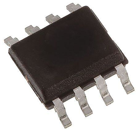
| 描述 | IC OPAMP GP 4MHZ 8SOIC运算放大器 - 运放 Gen Purp FET-Input Oper Amplifier |
| 产品分类 | Linear - Amplifiers - Instrumentation, OP Amps, Buffer Amps集成电路 - IC |
| 品牌 | Texas Instruments |
| 产品手册 | |
| 产品图片 |
|
| rohs | 符合RoHS无铅 / 符合限制有害物质指令(RoHS)规范要求 |
| 产品系列 | 放大器 IC,运算放大器 - 运放,Texas Instruments OPA131UA- |
| 数据手册 | |
| 产品型号 | OPA131UA |
| 产品目录页面 | |
| 产品种类 | 运算放大器 - 运放 |
| 供应商器件封装 | 8-SOIC |
| 共模抑制比—最小值 | 70 dB |
| 关闭 | No Shutdown |
| 包装 | 管件 |
| 单位重量 | 76 mg |
| 压摆率 | 10 V/µs |
| 双重电源电压 | +/- 15 V |
| 商标 | Texas Instruments |
| 增益带宽生成 | 4 MHz |
| 增益带宽积 | 4MHz |
| 安装类型 | 表面贴装 |
| 安装风格 | SMD/SMT |
| 封装 | Tube |
| 封装/外壳 | 8-SOIC(0.154",3.90mm 宽) |
| 封装/箱体 | SOIC-8 |
| 工作温度 | -40°C ~ 85°C |
| 工作电源电压 | 9 V to 36 V, +/- 4.5 V to +/- 18 V |
| 工厂包装数量 | 75 |
| 技术 | JFET |
| 放大器类型 | Low Noise Amplifier |
| 最大双重电源电压 | +/- 18 V |
| 最大工作温度 | + 85 C |
| 最小双重电源电压 | +/- 4.5 V |
| 最小工作温度 | - 40 C |
| 标准包装 | 75 |
| 电压-电源,单/双 (±) | 9 V ~ 36 V, ±4.5 V ~ 18 V |
| 电压-输入失调 | 200µV |
| 电流-电源 | 1.5mA |
| 电流-输入偏置 | 5pA |
| 电流-输出/通道 | 25mA |
| 电源电流 | 1.75 mA |
| 电路数 | 1 |
| 系列 | OPA131 |
| 转换速度 | 10 V/us |
| 输入偏压电流—最大 | 50 pA |
| 输入参考电压噪声 | 21 nV |
| 输入补偿电压 | 1 mV |
| 输出电流 | 25 mA |
| 输出类型 | - |
| 通道数量 | 1 Channel |


- 商务部:美国ITC正式对集成电路等产品启动337调查
- 曝三星4nm工艺存在良率问题 高通将骁龙8 Gen1或转产台积电
- 太阳诱电将投资9.5亿元在常州建新厂生产MLCC 预计2023年完工
- 英特尔发布欧洲新工厂建设计划 深化IDM 2.0 战略
- 台积电先进制程称霸业界 有大客户加持明年业绩稳了
- 达到5530亿美元!SIA预计今年全球半导体销售额将创下新高
- 英特尔拟将自动驾驶子公司Mobileye上市 估值或超500亿美元
- 三星加码芯片和SET,合并消费电子和移动部门,撤换高东真等 CEO
- 三星电子宣布重大人事变动 还合并消费电子和移动部门
- 海关总署:前11个月进口集成电路产品价值2.52万亿元 增长14.8%


PDF Datasheet 数据手册内容提取
OPA131 OPA2131 OPA131 OPA2131 OPA4131 OPA131 OPA2131 OPA4131 OPA4131 OPA4131 SBOS040A – NOVEMBER 1994 – REVISED DECEMBER 2002 General-Purpose FET-INPUT OPERATIONAL AMPLIFIERS FEATURES (cid:1) FET INPUT: I = 50pA max B (cid:1) LOW OFFSET VOLTAGE: 750µV max OPA131 (cid:1) WIDE SUPPLY RANGE: ±4.5V to ±18V Offset Trim 1 8 NC (cid:1) SLEW RATE: 10V/µs –In 2 7 V+ (cid:1) WIDE BANDWIDTH: 4MHz +In 3 6 Output (cid:1) EXCELLENT CAPACITIVE LOAD DRIVE V– 4 5 Offset Trim (cid:1) SINGLE, DUAL, QUAD VERSIONS DIP-8, SO-8 DESCRIPTION The OPA131 series of FET-input op amps provides high OPA2131 performance at low cost. Single, dual, and quad versions in industry-standard pinouts allow cost-effective design op- Out A 1 8 V+ tions. A –In A 2 7 Out B The OPA131 series offers excellent general-purpose perfor- mance, including low offset voltage, drift, and good dynamic +In A 3 B 6 –In B characteristics. V– 4 5 +In B Single, dual, and quad versions are available in DIP and SO packages. Performance grades include commercial and in- DIP-8, SO-8 dustrial temperature ranges. OPA4131 OPA4131 Out A 1 14 Out D Out A 1 16 Out D –In A 2 13 –In D –In A 2 15 –In D A D A D +In A 3 12 +In D +In A 3 14 +In D V+ 4 11 V– V+ 4 13 V– +In B 5 10 +In C +In B 5 12 +In C B C B C –In B 6 9 –In C –In B 6 11 –In C Out B 7 8 Out C Out B 7 10 Out C NC 8 9 NC DIP-14, SO-14 NC = No Connection SOL-16 Please be aware that an important notice concerning availability, standard warranty, and use in critical applications of Texas Instruments semiconductor products and disclaimers thereto appears at the end of this data sheet. PRODUCTION DATA information is current as of publication date. Copyright © 1994, Texas Instruments Incorporated Products conform to specifications per the terms of Texas Instruments standard warranty. Production processing does not necessarily include testing of all parameters. www.ti.com
ABSOLUTE MAXIMUM RATINGS(1) ELECTROSTATIC Supply Voltage, V+ to V–....................................................................36V DISCHARGE SENSITIVITY Input Voltage..................................................(V–) – 0.7V to (V+) + 0.7V Output Short-Circuit(2)..............................................................Continuous Operating Temperature..................................................–55°C to +125°C This integrated circuit can be damaged by ESD. Texas Instru- Storage Temperature.....................................................–55°C to +125°C ments recommends that all integrated circuits be handled with Junction Temperature......................................................................150°C appropriate precautions. Failure to observe proper handling Lead Temperature (soldering, 10s).................................................300°C and installation procedures can cause damage. NOTES: (1) Stresses above these ratings may cause permanent damage. Exposure to absolute maximum conditions for extended periods may degrade ESD damage can range from subtle performance degradation device reliability. (2) Short-circuit to ground, one amplifier per package. to complete device failure. Precision integrated circuits may be more susceptible to damage because very small parametric changes could cause the device not to meet its published specifications. PACKAGE/ORDERING INFORMATION SPECIFIED PACKAGE TEMPERATURE PACKAGE ORDERING TRANSPORT PRODUCT PACKAGE-LEAD DESIGNATOR(1) RANGE MARKING NUMBER MEDIA, QUANTITY Single OPA131 SO-8 D –40°C to +85°C OPA131UJ OPA131UJ Rails, 100 " " " " " OPA131UJ/2K5 Tape and Reel, 2500 OPA131 SO-8 D –40°C to +85°C OPA131UA OPA131UA Rails, 100 " " " " " OPA131UA/2K5 Tape and Reel, 2500 OPA131 SO-8 D –40°C to +85°C OPA131U OPA131U Rails, 100 " " " " " OPA131U/2K5 Tape and Reel, 2500 Dual OPA2131 SO-8 D –40°C to +85°C OPA2131UJ OPA2131UJ Rails, 100 " " " " " OPA2131UJ/2K5 Tape and Reel, 2500 OPA2131 SO-8 D –40°C to +85°C OPA2131UA OPA2131UA Rails, 100 " " " " " OPA2131UA/2K5 Tape and Reel, 2500 Quad OPA4131 DIP-14 N –40°C to +85°C OPA4131PJ OPA4131PJ Rails, 25 " " " " OPA4131PA OPA4131PA Rails, 25 OPA4131 SOL-16 DW –40°C to +85°C OPA4131UA OPA4131UA Rails, 48 " " " " " OPA4131UA/1K Tape and Reel, 1000 OPA4131 SOL-14 D –40°C to +85°C OPA4131NJ OPA4131NJ Rails, 58 " " " " OPA4131NA OPA4131NA Rails, 58 NOTE: (1) For the most current specifications and package information, refer to our web site at www.ti.com. OPA131, 2131, 4131 2 www.ti.com SBOS040A
ELECTRICAL CHARACTERISTICS At T = +25°C, V = ±15V, and R = 2kΩ, unless otherwise noted. A S L OPA131UA OPA131UJ OPA2131UA OPA2131UJ OPA4131PA, UA, NA OPA4131PJ, NJ PARAMETER CONDITION MIN TYP MAX MIN TYP MAX UNITS OFFSET VOLTAGE Input Offset Voltage ±0.2 ±1 ✻ ±1.5 mV OPA131U model only ±0.2 0.75 mV vs Temperature(1) Operating Temperature Range ±2 ±10 ✻ ✻ µV/°C vs Power Supply V = ±4.5V to ±18V 50 200 ✻ ✻ µV/V S OPA131U model only 50 100 µV/V INPUT BIAS CURRENT(2) Input Bias Current V = 0V +5 ±50 ✻ ✻ pA CM vs Temperature See Typical Characteristic ✻ Input Offset Current V = 0V ±1 ±50 ✻ ✻ pA CM NOISE Input Voltage Noise Noise Density, f = 10Hz 21 ✻ nV/√Hz f = 100Hz 16 ✻ nV/√Hz f = 1kHz 15 ✻ nV/√Hz f = 10kHz 15 ✻ nV/√Hz Current Noise Density, f = 1kHz 3 ✻ fA/√Hz INPUT VOLTAGE RANGE Common-Mode Voltage Range (V–) + 3 (V+) – 1 ✻ ✻ V Common-Mode Rejection V = –12V to +14V 70 80 ✻ ✻ dB CM OPA131U model only 80 86 dB INPUT IMPEDANCE Differential 1010 || 1 ✻ Ω || pF Common-Mode V = 0V 1012 || 3 ✻ Ω || pF CM OPEN-LOOP GAIN Open-Loop Voltage Gain V = –12V to +12V 94 110 ✻ ✻ dB O OPA131U model only 100 110 dB FREQUENCY RESPONSE Gain-Bandwidth Product 4 ✻ MHz Slew Rate 10 ✻ V/µs Settling Time 0.1% G = –1, 10V Step, C = 100pF 1.5 ✻ µs L 0.01% G = –1, 10V Step, C = 100pF 2 ✻ µs L Total Harmonic Distortion + Noise 1kHz, G = 1, V = 3.5Vrms 0.0008 ✻ % O OUTPUT Voltage Output, Positive (V+) – 3 (V+) – 2.5 ✻ ✻ V Negative (V–) + 3 (V–) + 2.5 ✻ ✻ V Short-Circuit Current ±25 ✻ mA POWER SUPPLY Specified Operating Voltage ±15 ✻ V Operating Voltage Range ±4.5 ±18 ✻ ✻ V Quiescent Current (per amplifier) I = 0 ±1.5 ±1.75 ✻ ±2 mA O TEMPERATURE RANGE Operating Range –55 +125 –55 +125 °C Storage –55 +125 ✻ ✻ °C Thermal Resistance, θ JA DIP-8 100 ✻ °C/W SO-8 150 ✻ °C/W DIP-14 80 ✻ °C/W SO-14, SOL-16 110 ✻ °C/W ✻ Specifications same as OPA131UA. NOTES: (1) Ensured by wafer test. (2) High-speed test at T = 25°C. J OPA131, 2131, 4131 3 SBOS040A www.ti.com
TYPICAL CHARACTERISTICS At T = +25°C, V = ±15V, and R = 2kΩ, unless otherwise noted. A S L POWER SUPPLY AND COMMON-MODE REJECTION OPEN-LOOP GAIN/PHASE vs FREQUENCY vs FREQUENCY 120 0 120 120 Voltage Gain (dB) 10864200000 G ∅ –––4915035°Phase Shift () wer Supply Rejection (dB) 186400000 CMR –P+SPRSR 186400000 mmon-Mode Rejection (dB) 0 –180 Po 20 20 Co –20 0 0 1 10 100 1k 10k 100k 1M 10M 10 100 1k 10k 100k 1M Frequency (Hz) Frequency (Hz) INPUT VOLTAGE AND CURRENT NOISE SPECTRAL DENSITY vs FREQUENCY CHANNEL SEPARATION vs FREQUENCY 1k 1k 160 R = ∞ L √oise (nV/Hz) 100 Voltage Noise 100 √oise (fA/Hz) eparation (dB) 114200 Voltage N 10 10 Current N Channel S 100 DGQA u ut=oaa ld1 Da ,m n oaderl laBq csu htuaoard enC dnd— eeclvhosiat.chneensre.l RL = 2kΩ combinations yield improved Current Noise rejection. 1 1 80 1 10 100 1k 10k 100k 1M 10 100 1k 10k 100k Frequency (Hz) Frequency (Hz) INPUT BIAS AND INPUT OFFSET CURRENT INPUT BIAS CURRENT vs TEMPERATURE vs INPUT COMMON-MODE VOLTAGE 10k 1k A) Input bias current is a ent (p 1k fbuentcwteioenn o tfh teh eV –v oslutapgpely Offset Curr 100 VCM = 0V IB IOS urrent (pA) 100 and the inputs. nd Input 101 ut Bias C 10 VS = ±15V a p as In Bi 0.1 put VS = ±5V In 0.01 1 –75 –50 –25 0 25 50 75 100 125 –15 –10 –5 0 5 10 15 Ambient Temperature (°C) Common-Mode Voltage (V) OPA131, 2131, 4131 4 www.ti.com SBOS040A
TYPICAL CHARACTERISTICS (Cont.) At T = +25°C, V = ±15V, and R = 2kΩ, unless otherwise noted. A S L QUIESCENT CURRENT AND SHORT-CIRCUIT CURRENT OPEN-LOOP GAIN vs TEMPERATURE vs TEMPERATURE 120 1.8 40 I 115 A) 1.6 ISC– VS = Q±15V 30 A) Voltage Gain (dB) 111005 Quiescent Current (m 11..42 ISC+ VS =IQ ±5V 2100 Short-Circuit Current (m 100 1 0 –75 –50 –25 0 25 50 75 100 125 –75 –50 –25 0 25 50 75 100 125 Ambient Temperature (°C) Temperature (°C) OFFSET VOLTAGE OFFSET VOLTAGE DRIFT PRODUCTION DISTRIBUTION PRODUCTION DISTRIBUTION 20 35 Typical production distribution Typical production distribution of packaged units. Single, 30 of packaged units. Single, dual and quad units included. dual and quad units included. 15 25 %) %) 20 Units ( 10 Units ( 15 10 5 5 0 0 0 0 0 0 0 0 0 0 0 0 0 0 0 0 0 –7 –6 –5 –4 –3 –2 –1 0 1 2 3 4 5 6 7 0 0 0 0 0 0 0 0 0 0 0 0 0 0 4 2 0 8 6 4 2 2 4 6 8 0 2 4 –1 –1 –1 – – – – 1 1 1 Offset Voltage Drift (µV/°C) Offset Voltage (µV) TOTAL HARMONIC DISTORTION + NOISE MAXIMUM OUTPUT VOLTAGE vs FREQUENCY vs FREQUENCY 1 30 Bandwidth- V = ±15V S V = 3.5Vrms Limited O 0.1 p) %) Vp- 20 Maximum output voltage + Noise ( 0.01 G = 100V/V Voltage ( wdiisthtoorutito snl.ew-rate induced HD G = 10V/V put 10 T ut V = ±5V 0.001 O S G = 1V/V 0.0001 0 10 100 1k 10k 100k 10k 100k 1M 10M Frequency (Hz) Frequency (Hz) OPA131, 2131, 4131 5 SBOS040A www.ti.com
TYPICAL CHARACTERISTICS (Cont.) At T = +25°C, V = ±15V, and R = 2kΩ, unless otherwise noted. CASE S L SMALL-SIGNAL STEP RESPONSE LARGE-SIGNAL STEP RESPONSE G =1, C = 300pF G = 1, C = 300pF L L v mV/di V/div 0 5 5 200ns/div 1µs/div SMALL-SIGNAL OVERSHOOT SETTLING TIME vs CLOSED-LOOP GAIN vs LOAD CAPACITANCE 100 50 R = 2kΩ V = 10V Step L RO = 2kΩ Higher RL value CLL = 100pF 40 goveenresrhaolloy tr.educes G = +2 G = –1 s) µTime ( 10 oot (%) 30 ettling 0.01% Oversh 20 G = 1 G = ±10 S 0.1% 10 1 0 –1 –10 –100 –1000 100pF 1nF 10nF Closed-Loop Gain (V/V) Load Capacitance OUTPUT VOLTAGE SWING vs OUTPUT CURRENT 15 V = 15V 14 IN g (V) 1132 25°C –55°C win 11 S 125°C e 10 g ut Volta ––1101 125°C 25°C utp –12 –55°C O –13 –14 V = –15V –15 IN 0 5 10 15 20 25 30 Output Current (mA) OPA131, 2131, 4131 6 www.ti.com SBOS040A
APPLICATIONS INFORMATION V+ The OPA131 series op amps are unity-gain stable and suitable for a wide range of general-purpose applications. 7 OPA131 (Single op amp only) Power-supply pins should be bypassed with 10nF ceramic 2 capacitors or larger. 6 OPA131 3 5 The OPA131 series op amps are free from unexpected 1 output phase-reversal common with FET op amps. Many 4 100kΩ FET-input op amps exhibit phase-reversal of the output when the input common-mode voltage range is exceeded. This can Trim Range: ±20mV typ occur in voltage-follower circuits, causing serious problems in control-loop applications. All circuitry is completely inde- V– pendent in dual and quad versions, assuring normal behavior when one amplifier in a package is overdriven or short- FIGURE 1. OPA131 Offset Voltage Trim Circuit. circuited. OFFSET VOLTAGE TRIM INPUT BIAS CURRENT The input bias current is approximately 5pA at room tem- The OPA131 (single op amp version) provides offset volt- perature and increases with temperature as shown in the age trim connections on pins 1 and 5. Offset voltage can be typical characteristic “Input Bias Current vs Temperature.” adjusted by connecting a potentiometer as shown in Figure 1. This adjustment should be used only to null the offset of Input bias current also varies with common-mode voltage the op amp, not system offset or offset produced by the and power supply voltage. This variation is dependent on the signal source. voltage between the negative power supply and the com- mon-mode input voltage. The effect is shown in the typical curve “Input Bias Current vs Common-Mode Voltage.” OPA131, 2131, 4131 7 SBOS040A www.ti.com
PACKAGE OPTION ADDENDUM www.ti.com 6-Feb-2020 PACKAGING INFORMATION Orderable Device Status Package Type Package Pins Package Eco Plan Lead/Ball Finish MSL Peak Temp Op Temp (°C) Device Marking Samples (1) Drawing Qty (2) (6) (3) (4/5) OPA131U ACTIVE SOIC D 8 75 Green (RoHS NIPDAU-DCC Level-3-260C-168 HR -55 to 125 OPA & no Sb/Br) 131U OPA131UA ACTIVE SOIC D 8 75 Green (RoHS NIPDAU-DCC Level-3-260C-168 HR -55 to 125 OPA & no Sb/Br) 131U A OPA131UA/2K5 ACTIVE SOIC D 8 2500 Green (RoHS NIPDAU-DCC Level-3-260C-168 HR -55 to 125 OPA & no Sb/Br) 131U A OPA131UJ ACTIVE SOIC D 8 75 Green (RoHS NIPDAU-DCC Level-3-260C-168 HR -55 to 125 OPA & no Sb/Br) 131UJ OPA131UJ/2K5 ACTIVE SOIC D 8 2500 Green (RoHS NIPDAU-DCC Level-3-260C-168 HR -55 to 125 OPA & no Sb/Br) 131UJ OPA2131UA ACTIVE SOIC D 8 75 Green (RoHS NIPDAU-DCC Level-3-260C-168 HR -55 to 125 OPA & no Sb/Br) 2131UA OPA2131UA/2K5 ACTIVE SOIC D 8 2500 Green (RoHS NIPDAU-DCC Level-3-260C-168 HR -55 to 125 OPA & no Sb/Br) 2131UA OPA2131UA/2K5G4 ACTIVE SOIC D 8 2500 Green (RoHS NIPDAU-DCC Level-3-260C-168 HR -55 to 125 OPA & no Sb/Br) 2131UA OPA2131UAE4 ACTIVE SOIC D 8 75 Green (RoHS NIPDAU-DCC Level-3-260C-168 HR -55 to 125 OPA & no Sb/Br) 2131UA OPA2131UAG4 ACTIVE SOIC D 8 75 Green (RoHS NIPDAU-DCC Level-3-260C-168 HR -55 to 125 OPA & no Sb/Br) 2131UA OPA2131UJ ACTIVE SOIC D 8 75 Green (RoHS NIPDAU-DCC Level-3-260C-168 HR OPA & no Sb/Br) 2131UJ OPA2131UJ/2K5 ACTIVE SOIC D 8 2500 Green (RoHS NIPDAU-DCC Level-3-260C-168 HR OPA & no Sb/Br) 2131UJ OPA4131NA ACTIVE SOIC D 14 50 Green (RoHS NIPDAU-DCC Level-3-260C-168 HR -40 to 85 OPA4131NA & no Sb/Br) OPA4131NAG4 ACTIVE SOIC D 14 50 Green (RoHS NIPDAU-DCC Level-3-260C-168 HR -40 to 85 OPA4131NA & no Sb/Br) OPA4131NJ ACTIVE SOIC D 14 50 Green (RoHS NIPDAU-DCC Level-3-260C-168 HR -40 to 85 OPA4131NJ & no Sb/Br) OPA4131PA ACTIVE PDIP N 14 25 Green (RoHS NIPDAU N / A for Pkg Type -40 to 85 OPA4131PA & no Sb/Br) Addendum-Page 1
PACKAGE OPTION ADDENDUM www.ti.com 6-Feb-2020 Orderable Device Status Package Type Package Pins Package Eco Plan Lead/Ball Finish MSL Peak Temp Op Temp (°C) Device Marking Samples (1) Drawing Qty (2) (6) (3) (4/5) OPA4131PAG4 ACTIVE PDIP N 14 25 Green (RoHS NIPDAU N / A for Pkg Type -40 to 85 OPA4131PA & no Sb/Br) OPA4131PJ ACTIVE PDIP N 14 25 Green (RoHS NIPDAU N / A for Pkg Type -40 to 85 OPA4131PJ & no Sb/Br) OPA4131UA ACTIVE SOIC DW 16 40 Green (RoHS NIPDAU-DCC Level-3-260C-168 HR -40 to 85 OPA4131UA & no Sb/Br) OPA4131UA/1K ACTIVE SOIC DW 16 1000 Green (RoHS NIPDAU-DCC Level-3-260C-168 HR -40 to 85 OPA4131UA & no Sb/Br) (1) The marketing status values are defined as follows: ACTIVE: Product device recommended for new designs. LIFEBUY: TI has announced that the device will be discontinued, and a lifetime-buy period is in effect. NRND: Not recommended for new designs. Device is in production to support existing customers, but TI does not recommend using this part in a new design. PREVIEW: Device has been announced but is not in production. Samples may or may not be available. OBSOLETE: TI has discontinued the production of the device. (2) RoHS: TI defines "RoHS" to mean semiconductor products that are compliant with the current EU RoHS requirements for all 10 RoHS substances, including the requirement that RoHS substance do not exceed 0.1% by weight in homogeneous materials. Where designed to be soldered at high temperatures, "RoHS" products are suitable for use in specified lead-free processes. TI may reference these types of products as "Pb-Free". RoHS Exempt: TI defines "RoHS Exempt" to mean products that contain lead but are compliant with EU RoHS pursuant to a specific EU RoHS exemption. Green: TI defines "Green" to mean the content of Chlorine (Cl) and Bromine (Br) based flame retardants meet JS709B low halogen requirements of <=1000ppm threshold. Antimony trioxide based flame retardants must also meet the <=1000ppm threshold requirement. (3) MSL, Peak Temp. - The Moisture Sensitivity Level rating according to the JEDEC industry standard classifications, and peak solder temperature. (4) There may be additional marking, which relates to the logo, the lot trace code information, or the environmental category on the device. (5) Multiple Device Markings will be inside parentheses. Only one Device Marking contained in parentheses and separated by a "~" will appear on a device. If a line is indented then it is a continuation of the previous line and the two combined represent the entire Device Marking for that device. (6) Lead/Ball Finish - Orderable Devices may have multiple material finish options. Finish options are separated by a vertical ruled line. Lead/Ball Finish values may wrap to two lines if the finish value exceeds the maximum column width. Important Information and Disclaimer:The information provided on this page represents TI's knowledge and belief as of the date that it is provided. TI bases its knowledge and belief on information provided by third parties, and makes no representation or warranty as to the accuracy of such information. Efforts are underway to better integrate information from third parties. TI has taken and continues to take reasonable steps to provide representative and accurate information but may not have conducted destructive testing or chemical analysis on incoming materials and chemicals. TI and TI suppliers consider certain information to be proprietary, and thus CAS numbers and other limited information may not be available for release. Addendum-Page 2
PACKAGE OPTION ADDENDUM www.ti.com 6-Feb-2020 In no event shall TI's liability arising out of such information exceed the total purchase price of the TI part(s) at issue in this document sold by TI to Customer on an annual basis. Addendum-Page 3
PACKAGE MATERIALS INFORMATION www.ti.com 9-Sep-2013 TAPE AND REEL INFORMATION *Alldimensionsarenominal Device Package Package Pins SPQ Reel Reel A0 B0 K0 P1 W Pin1 Type Drawing Diameter Width (mm) (mm) (mm) (mm) (mm) Quadrant (mm) W1(mm) OPA131UA/2K5 SOIC D 8 2500 330.0 12.4 6.4 5.2 2.1 8.0 12.0 Q1 OPA131UJ/2K5 SOIC D 8 2500 330.0 12.4 6.4 5.2 2.1 8.0 12.0 Q1 OPA2131UA/2K5 SOIC D 8 2500 330.0 12.4 6.4 5.2 2.1 8.0 12.0 Q1 OPA2131UJ/2K5 SOIC D 8 2500 330.0 12.4 6.4 5.2 2.1 8.0 12.0 Q1 OPA4131UA/1K SOIC DW 16 1000 330.0 16.4 10.75 10.7 2.7 12.0 16.0 Q1 PackMaterials-Page1
PACKAGE MATERIALS INFORMATION www.ti.com 9-Sep-2013 *Alldimensionsarenominal Device PackageType PackageDrawing Pins SPQ Length(mm) Width(mm) Height(mm) OPA131UA/2K5 SOIC D 8 2500 367.0 367.0 35.0 OPA131UJ/2K5 SOIC D 8 2500 367.0 367.0 35.0 OPA2131UA/2K5 SOIC D 8 2500 367.0 367.0 35.0 OPA2131UJ/2K5 SOIC D 8 2500 367.0 367.0 35.0 OPA4131UA/1K SOIC DW 16 1000 367.0 367.0 38.0 PackMaterials-Page2
GENERIC PACKAGE VIEW DW 16 SOIC - 2.65 mm max height 7.5 x 10.3, 1.27 mm pitch SMALL OUTLINE INTEGRATED CIRCUIT This image is a representation of the package family, actual package may vary. Refer to the product data sheet for package details. 4224780/A www.ti.com
PACKAGE OUTLINE DW0016A SOIC - 2.65 mm max height SCALE 1.500 SOIC C 10.63 SEATING PLANE TYP 9.97 A PIN 1 ID 0.1 C AREA 14X 1.27 16 1 10.5 2X 10.1 8.89 NOTE 3 8 9 0.51 16X 0.31 7.6 B 7.4 0.25 C A B 2.65 MAX NOTE 4 0.33 TYP 0.10 SEE DETAIL A 0.25 GAGE PLANE 0.3 0 - 8 0.1 1.27 0.40 DETAIL A (1.4) TYPICAL 4220721/A 07/2016 NOTES: 1. All linear dimensions are in millimeters. Dimensions in parenthesis are for reference only. Dimensioning and tolerancing per ASME Y14.5M. 2. This drawing is subject to change without notice. 3. This dimension does not include mold flash, protrusions, or gate burrs. Mold flash, protrusions, or gate burrs shall not exceed 0.15 mm, per side. 4. This dimension does not include interlead flash. Interlead flash shall not exceed 0.25 mm, per side. 5. Reference JEDEC registration MS-013. www.ti.com
EXAMPLE BOARD LAYOUT DW0016A SOIC - 2.65 mm max height SOIC 16X (2) SEE SYMM DETAILS 1 16 16X (0.6) SYMM 14X (1.27) 8 9 R0.05 TYP (9.3) LAND PATTERN EXAMPLE SCALE:7X METAL SOLDER MASK SOLDER MASK METAL OPENING OPENING 0.07 MAX 0.07 MIN ALL AROUND ALL AROUND NON SOLDER MASK SOLDER MASK DEFINED DEFINED SOLDER MASK DETAILS 4220721/A 07/2016 NOTES: (continued) 6. Publication IPC-7351 may have alternate designs. 7. Solder mask tolerances between and around signal pads can vary based on board fabrication site. www.ti.com
EXAMPLE STENCIL DESIGN DW0016A SOIC - 2.65 mm max height SOIC 16X (2) SYMM 1 16 16X (0.6) SYMM 14X (1.27) 8 9 R0.05 TYP (9.3) SOLDER PASTE EXAMPLE BASED ON 0.125 mm THICK STENCIL SCALE:7X 4220721/A 07/2016 NOTES: (continued) 8. Laser cutting apertures with trapezoidal walls and rounded corners may offer better paste release. IPC-7525 may have alternate design recommendations. 9. Board assembly site may have different recommendations for stencil design. www.ti.com
None
None
PACKAGE OUTLINE D0008A SOIC - 1.75 mm max height SCALE 2.800 SMALL OUTLINE INTEGRATED CIRCUIT C SEATING PLANE .228-.244 TYP [5.80-6.19] .004 [0.1] C A PIN 1 ID AREA 6X .050 [1.27] 8 1 2X .189-.197 [4.81-5.00] .150 NOTE 3 [3.81] 4X (0 -15 ) 4 5 8X .012-.020 B .150-.157 [0.31-0.51] .069 MAX [3.81-3.98] .010 [0.25] C A B [1.75] NOTE 4 .005-.010 TYP [0.13-0.25] 4X (0 -15 ) SEE DETAIL A .010 [0.25] .004-.010 0 - 8 [0.11-0.25] .016-.050 [0.41-1.27] DETAIL A (.041) TYPICAL [1.04] 4214825/C 02/2019 NOTES: 1. Linear dimensions are in inches [millimeters]. Dimensions in parenthesis are for reference only. Controlling dimensions are in inches. Dimensioning and tolerancing per ASME Y14.5M. 2. This drawing is subject to change without notice. 3. This dimension does not include mold flash, protrusions, or gate burrs. Mold flash, protrusions, or gate burrs shall not exceed .006 [0.15] per side. 4. This dimension does not include interlead flash. 5. Reference JEDEC registration MS-012, variation AA. www.ti.com
EXAMPLE BOARD LAYOUT D0008A SOIC - 1.75 mm max height SMALL OUTLINE INTEGRATED CIRCUIT 8X (.061 ) [1.55] SYMM SEE DETAILS 1 8 8X (.024) [0.6] SYMM (R.002 ) TYP [0.05] 5 4 6X (.050 ) [1.27] (.213) [5.4] LAND PATTERN EXAMPLE EXPOSED METAL SHOWN SCALE:8X SOLDER MASK SOLDER MASK METAL OPENING OPENING METAL UNDER SOLDER MASK EXPOSED METAL EXPOSED METAL .0028 MAX .0028 MIN [0.07] [0.07] ALL AROUND ALL AROUND NON SOLDER MASK SOLDER MASK DEFINED DEFINED SOLDER MASK DETAILS 4214825/C 02/2019 NOTES: (continued) 6. Publication IPC-7351 may have alternate designs. 7. Solder mask tolerances between and around signal pads can vary based on board fabrication site. www.ti.com
EXAMPLE STENCIL DESIGN D0008A SOIC - 1.75 mm max height SMALL OUTLINE INTEGRATED CIRCUIT 8X (.061 ) [1.55] SYMM 1 8 8X (.024) [0.6] SYMM (R.002 ) TYP [0.05] 5 4 6X (.050 ) [1.27] (.213) [5.4] SOLDER PASTE EXAMPLE BASED ON .005 INCH [0.125 MM] THICK STENCIL SCALE:8X 4214825/C 02/2019 NOTES: (continued) 8. Laser cutting apertures with trapezoidal walls and rounded corners may offer better paste release. IPC-7525 may have alternate design recommendations. 9. Board assembly site may have different recommendations for stencil design. www.ti.com
None
IMPORTANTNOTICEANDDISCLAIMER TI PROVIDES TECHNICAL AND RELIABILITY DATA (INCLUDING DATASHEETS), DESIGN RESOURCES (INCLUDING REFERENCE DESIGNS), APPLICATION OR OTHER DESIGN ADVICE, WEB TOOLS, SAFETY INFORMATION, AND OTHER RESOURCES “AS IS” AND WITH ALL FAULTS, AND DISCLAIMS ALL WARRANTIES, EXPRESS AND IMPLIED, INCLUDING WITHOUT LIMITATION ANY IMPLIED WARRANTIES OF MERCHANTABILITY, FITNESS FOR A PARTICULAR PURPOSE OR NON-INFRINGEMENT OF THIRD PARTY INTELLECTUAL PROPERTY RIGHTS. These resources are intended for skilled developers designing with TI products. You are solely responsible for (1) selecting the appropriate TI products for your application, (2) designing, validating and testing your application, and (3) ensuring your application meets applicable standards, and any other safety, security, or other requirements. These resources are subject to change without notice. TI grants you permission to use these resources only for development of an application that uses the TI products described in the resource. Other reproduction and display of these resources is prohibited. No license is granted to any other TI intellectual property right or to any third party intellectual property right. TI disclaims responsibility for, and you will fully indemnify TI and its representatives against, any claims, damages, costs, losses, and liabilities arising out of your use of these resources. TI’s products are provided subject to TI’s Terms of Sale (www.ti.com/legal/termsofsale.html) or other applicable terms available either on ti.com or provided in conjunction with such TI products. TI’s provision of these resources does not expand or otherwise alter TI’s applicable warranties or warranty disclaimers for TI products. Mailing Address: Texas Instruments, Post Office Box 655303, Dallas, Texas 75265 Copyright © 2020, Texas Instruments Incorporated