ICGOO在线商城 > 集成电路(IC) > 线性 - 放大器 - 仪表,运算放大器,缓冲器放大器 > OPA1013DN8
 Datasheet下载
- 型号: OPA1013DN8
- 制造商: Texas Instruments
- 库位|库存: xxxx|xxxx
- 要求:
| 数量阶梯 | 香港交货 | 国内含税 |
| +xxxx | $xxxx | ¥xxxx |
查看当月历史价格
查看今年历史价格
OPA1013DN8产品简介:
ICGOO电子元器件商城为您提供OPA1013DN8由Texas Instruments设计生产,在icgoo商城现货销售,并且可以通过原厂、代理商等渠道进行代购。 OPA1013DN8价格参考¥18.99-¥35.28。Texas InstrumentsOPA1013DN8封装/规格:线性 - 放大器 - 仪表,运算放大器,缓冲器放大器, 通用 放大器 2 电路 8-PDIP。您可以下载OPA1013DN8参考资料、Datasheet数据手册功能说明书,资料中有OPA1013DN8 详细功能的应用电路图电压和使用方法及教程。
| 参数 | 数值 |
| -3db带宽 | - |
| 产品目录 | 集成电路 (IC)半导体 |
| 描述 | IC OPAMP GP 600KHZ 8DIP运算放大器 - 运放 Precision Single Supply Dual |
| 产品分类 | Linear - Amplifiers - Instrumentation, OP Amps, Buffer Amps集成电路 - IC |
| 品牌 | Texas Instruments |
| 产品手册 | http://www.ti.com/litv/sbos005 |
| 产品图片 |
|
| rohs | 符合RoHS无铅 / 符合限制有害物质指令(RoHS)规范要求 |
| 产品系列 | 放大器 IC,运算放大器 - 运放,Texas Instruments OPA1013DN8- |
| 数据手册 | |
| 产品型号 | OPA1013DN8 |
| 产品目录页面 | |
| 产品种类 | 运算放大器 - 运放 |
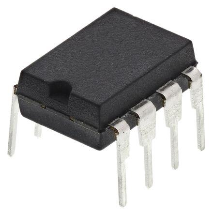
| 供应商器件封装 | 8-PDIP |
| 共模抑制比—最小值 | 97 dB |
| 关闭 | No Shutdown |
| 包装 | 管件 |
| 单位重量 | 523.200 mg |
| 压摆率 | 0.35 V/µs |
| 双重电源电压 | +/- 15 V |
| 商标 | Texas Instruments |
| 增益带宽生成 | 0.6 MHz |
| 增益带宽积 | 600kHz |
| 安装类型 | 通孔 |
| 安装风格 | Through Hole |
| 封装 | Tube |
| 封装/外壳 | 8-DIP(0.300",7.62mm) |
| 封装/箱体 | PDIP-8 |
| 工作温度 | 0°C ~ 70°C |
| 工作电源电压 | 4 V to 36 V, +/- 2 V to +/- 18 V |
| 工厂包装数量 | 50 |
| 技术 | Bipolar |
| 放大器类型 | 通用 |
| 最大双重电源电压 | +/- 18 V |
| 最大工作温度 | + 70 C |
| 最小双重电源电压 | +/- 2 V |
| 最小工作温度 | 0 C |
| 标准包装 | 50 |
| 电压-电源,单/双 (±) | 4 V ~ 36 V, ±2 V ~ 18 V |
| 电压-输入失调 | 200µV |
| 电流-电源 | 350µA |
| 电流-输入偏置 | 7nA |
| 电流-输出/通道 | - |
| 电源电流 | 0.55 mA |
| 电路数 | 2 |
| 系列 | OPA1013 |
| 转换速度 | 0.35 V/us |
| 输入偏压电流—最大 | 50 nA |
| 输入参考电压噪声 | 28 nV |
| 输入补偿电压 | 800 uV |
| 输出类型 | - |
| 通道数量 | 2 Channel |


- 商务部:美国ITC正式对集成电路等产品启动337调查
- 曝三星4nm工艺存在良率问题 高通将骁龙8 Gen1或转产台积电
- 太阳诱电将投资9.5亿元在常州建新厂生产MLCC 预计2023年完工
- 英特尔发布欧洲新工厂建设计划 深化IDM 2.0 战略
- 台积电先进制程称霸业界 有大客户加持明年业绩稳了
- 达到5530亿美元!SIA预计今年全球半导体销售额将创下新高
- 英特尔拟将自动驾驶子公司Mobileye上市 估值或超500亿美元
- 三星加码芯片和SET,合并消费电子和移动部门,撤换高东真等 CEO
- 三星电子宣布重大人事变动 还合并消费电子和移动部门
- 海关总署:前11个月进口集成电路产品价值2.52万亿元 增长14.8%


PDF Datasheet 数据手册内容提取
® OPA1013 Precision, Single-Supply DUAL OPERATIONAL AMPLIFIER FEATURES APPLICATIONS l SINGLE POWER SUPPLY OPERATION l PRECISION INSTRUMENTATION l INPUT VOLTAGE RANGE TO GROUND l BATTERY-POWERED EQUIPMENT l OUTPUT SWINGS NEAR GROUND l BRIDGE AMPLIFIERS l LOW QUIESCENT CURRENT: 550m A max l 4-20mA CURRENT TRANSMITTERS l LOW V : 300m V max l VOLTAGE COMPARATOR OS l LOW DRIFT: 2.5m V/(cid:176) C max l LOW I : 1.5nA max OS l LOW NOISE: 0.55m Vp-p, 0.1Hz to 10Hz DESCRIPTION The OPA1013 dual operational amplifier provides The OPA1013 is characterized for operation at both precision performance in single power supply and low +5V (single supply) and – 15V power supplies. When power applications. It is laser trimmed for low offset operated from a single supply, the input common-mode voltage and drift, greatly reducing the large errors range includes ground and the output can swing to common with LM324-type op amps. Input offset within 15mV of ground. Completely independent bias- current is also trimmed to reduce errors in high im- ing networks eliminate interaction between the two pedance applications. amplifiers—even when one is used as a comparator. The OPA1013 is available in an 8-pin plastic DIP specified for the 0(cid:176) C to +70(cid:176) C temperature range. V+(cid:13) 3.3µA 8 Simplified Circuit(cid:13) 3.3µA 7.5µA (Half of Dual) 2nd(cid:13) 400W 0.9V 400W SGtaagine(cid:13) 22W Out(cid:13) 1, 7 In –(cid:13) In +(cid:13) 2, 6 3, 5 22W V–(cid:13) 4 International Airport Industrial Park • Mailing Address: PO Box 11400 • Tucson, AZ 85734 • Street Address: 6730 S. Tucson Blvd. • Tucson, AZ 85706 Tel: (520) 746-1111 • Twx: 910-952-1111 • Cable: BBRCORP • Telex: 066-6491 • FAX: (520) 889-1510 • Immediate Product Info: (800) 548-6132 © 1990 Burr-Brown Corporation PDS-1059F Printed in U.S.A. December, 1994 SBOS005
SPECIFICATIONS ELECTRICAL V = – 15V, V = 0V, T = +25(cid:176)C unless otherwise noted. S CM A OPA1013CN8 OPA1013DN8 PARAMETER CONDITION MIN TYP MAX MIN TYP MAX UNITS Input Offset Voltage – 50 – 300 – 200 – 800 m V Time Stability 0.5 * m V/Mo Input Offset Current – 0.08 – 1.5 * * nA Input Bias Current 7 30 * * nA Voltage Noise, BW = 0.1 to 10Hz 0.55 * m Vp-p Noise Density, f = 10Hz 28 * nV/(cid:214) Hz f = 1kHz 25 * nV/(cid:214) Hz Current Noise Density, f = 10Hz 0.12 * pA/(cid:214) Hz Input Resistance: Differential 70 300 * * MW Input Resistance: Common-Mode 4 * GW Open-Loop Voltage Gain V = – 10V, R = 2kW 1.2 2.9 * * V/m V O L VO = – 10V, RL = 600W 0.5 1.9 * * V/m V Common-Mode Input Range +13.5 +13.8 * * V –15 –15.3 * * V Common-Mode Rejection V = +13.5 to –15V 97 114 * * dB CM Power Supply Rejection VS = – 2 to – 18V 100 117 * * dB Channel Separation V = – 10V, R = 2kW 120 137 * * dB O L Voltage Output RL = 2kW – 12.5 – 14 * * V Slew Rate 0.2 0.35 * * V/m s Quiescent Current (per amplifier) – 0.35 – 0.55 * * mA *Specification same as OPA1013CN8. VS = +5V/0V, VCM = 0V, VO = +1.4V, TA = +25(cid:176)C unless otherwise noted. OPA1013CN8 OPA1013DN8 PARAMETER CONDITION MIN TYP MAX MIN TYP MAX UNITS Input Offset Voltage – 90 – 450 – 250 – 950 m V Input Offset Current – 3.0 – 2.0 * * nA Input Bias Current 10 50 * * nA Open-Loop Voltage Gain VO = 5mV to 4V 0.1 * V/m V R = 500W L Common-Mode Input Range +3.5 +3.8 * * V 0 –0.3 * * V Voltage Output Low No Load 15 25 * * mV Low R = 600W to Ground 5 10 * * mV L Low ISINK = 1mA 200 350 * * mV High No Load 4 4.4 * * V High RL = 600W to Ground 3.4 4 * * V Quiescent Current (per amplifier) 0.33 0.5 * * mA *Specification same as OPA1013CN8. TA = 0(cid:176)C to +70(cid:176)C, VS = – 15V, VCM = 0V unless otherwise noted. OPA1013CN8 OPA1013DN8 PARAMETER CONDITION MIN TYP MAX MIN TYP MAX UNITS Input Offset Voltage – 80 – 400 – 230 – 1000 m V VS = +5/0V, VO = +1.4V – 110 – 570 – 280 – 1200 m V Input Offset Voltage Drift(1) 0.4 2.5 0.7 5 m V/(cid:176)C Input Offset Current – 0.3 – 2.8 * * nA V = +5/0V, V = +1.4V – 0.5 – 6 * * nA S O Input Bias Current 9 38 * * nA V = +5/0V, V = +1.4V 13 90 * * nA S O Open-Loop Voltage Gain VO = – 10V, RL = 2kW 0.7 2.2 * * V/m V Common-Mode Rejection V = +13 to –15V 94 113 * * dB CM Power Supply Rejection VS = – 2 to – 18V 97 116 * * dB Voltage Output R = 2kW – 12.0 – 13.9 * * V L VO Low VS = +5/0V, RL = 600W 6 13 * * mV V High V = +5/0V, R = 600W 3.2 3.9 * * V O S L Quiescent Current (per amplifier) – 0.37 – 0.6 * * mA V = +5/0V, V = +1.4V 0.34 0.55 * * mA S O *Specification same as OPA1013CN8. NOTE: (1) Guaranteed by design. This specification is established to a 98% confidence level. ® OPA1013 2
DICE INFORMATION PAD FUNCTION 1 Output A 2 –In A 3 +In A 4 V– 5 +In B 6 –In B 7 Output B 8 V+ 4 Substrate Bias: –V S MECHANICAL INFORMATION MILS (0.001") MILLIMETERS Die Size 112 x 100 – 5 2.84 x 2.54 – 0.13 Die Thickness 20 – 3 0.51 – 0.08 Min. Pad Size 4 x 4 0.10 x 0.10 Transistor Count 92 Backing Gold OPA1013 DIE TOPOGRAPHY CONNECTION DIAGRAM ABSOLUTE MAXIMUM RATINGS Power Supply Voltage.......................................................................– 22V N8 — Plastic Package — Top View Differential Input Voltage...................................................................– 30V Input Voltage......................................................................V+ to (V–) –5V Output Short Circuit (T = 25(cid:176)C).............................................Continuous A Operating Temperature:.......................................................0(cid:176)C to +70(cid:176)C Storage Temperature..........................................................–65 to +150(cid:176)C Out A(cid:13) 1(cid:13) 8(cid:13) V+(cid:13) Lead Temperature (soldering, 10s)...............................................+300(cid:176)C A – + –In A(cid:13) 2(cid:13) 7(cid:13) Out B(cid:13) B ORDERING INFORMATION + – +In A(cid:13) 3(cid:13) 6(cid:13) –In B(cid:13) MODEL PACKAGE TEMPERATURE RANGE OPA1013CN8 Plastic DIP 0(cid:176)C to +70(cid:176)C V– 4 5 +In B OPA1013DN8 Plastic DIP 0(cid:176)C to +70(cid:176)C PACKAGE INFORMATION PACKAGE DRAWING MODEL PACKAGE NUMBER(1) OPA1013CN8 Plastic DIP 006 OPA1013DN8 Plastic DIP 006 NOTE: (1) For detailed drawing and dimension table, please see end of data sheet, or Appendix D of Burr-Brown IC Data Book. The information provided herein is believed to be reliable; however, BURR-BROWN assumes no responsibility for inaccuracies or omissions. BURR-BROWN assumes no responsibility for the use of this information, and all use of such information shall be entirely at the user’s own risk. Prices and specifications are subject to change without notice. No patent rights or licenses to any of the circuits described herein are implied or granted to any third party. BURR-BROWN does not authorize or warrant any BURR-BROWN product for use in life support devices and/or systems. ® 3 OPA1013
TYPICAL PERFORMANCE CURVES T = +25(cid:176)C unless otherwise noted. A OFFSET VOLTAGE(cid:13) OFFSET VOLTAGE vs TEMPERATURE vs BALANCED SOURCE RESISTANCE 10 200(cid:13) VS = ±15V R + V) Offset Voltage (µV) –1100000(cid:13)(cid:13)(cid:13) put Offset Voltage (m 0.11 R – V S = 5V/0V, 25°CV S = ±15V, 25°C n I –200 6 Representative Devices 0.01 –50 –25 0 25 50 75 100 125 1k 3k 10k 30k 100k 300k 1M 3M 10M Temperature (°C) Balanced Source Resistor (W ) COMMON-MODE REJECTION RATIO(cid:13) OFFSET VOLTAGE vs TIME vs FREQUENCY 5(cid:13) 120(cid:13) µV) 4(cid:13) VS = ±15V o (dB) 100(cid:13) ge ( Rati V = ±15V s in Offset Volta 32(cid:13)(cid:13) Plastic DIP N8 Package Mode Rejection 864000(cid:13)(cid:13)(cid:13) V = 5V/0V ge n- Chan 1(cid:13) mmo 20(cid:13) o C 0 0 0 1 2 3 4 5 10 100 1k 10k 100k 1M Time After Power On (Minutes) Frequency (Hz) POWER SUPPLY REJECTION RATIO(cid:13) vs FREQUENCY 0.1Hz TO 10Hz NOISE 120(cid:13) B) VS = ±2V to ±18V atio (d 100(cid:13) NSeugpaptilvye(cid:13) Div) n R 80(cid:13) nV/ o 0 Rejecti 60(cid:13) PSouspitpivlye(cid:13) ge (20 pply 40(cid:13) Volta Su se wer 20(cid:13) Noi o P 0 0.1 1 10 100 1k 10k 100k 1M 0 2 4 6 8 10 Frequency (Hz) Time (s) ® OPA1013 4
TYPICAL PERFORMANCE CURVES (CONT) T = +25(cid:176)C unless otherwise noted. A NOISE DENSITY vs FREQUENCY 10Hz VOLTAGE NOISE DISTRIBUTION 1000 200(cid:13) V = ±2V to ±18V VS = ±15V(cid:13) Voltage Noise Density (nV/ Hz)(cid:13)Current Noise Density (fA/ Hz) 31003000 CNVouolritsraeegnet(cid:13)(cid:13) Number of Units 11111864208642000000000(cid:13)(cid:13)(cid:13)(cid:13)(cid:13)(cid:13)(cid:13)(cid:13)(cid:13) 3fr4o0m u tnhirtese t erustnesd.(cid:13) Noise 10 0 1 10 100 1k 10 20 30 40 50 60 Frequency (Hz) Voltage Noise Density (nV/ Hz) INPUT BIAS CURRENT(cid:13) SUPPLY CURRENT vs TEMPERATURE vs COMMON-MODE VOLTAGE Supply Current per Amplifier (µA) 443336284000000(cid:13)(cid:13)(cid:13)(cid:13)(cid:13) VS V S = =5 V±/105VV mmon-Mode Input Voltage, V = ±15V (V)S–11–1505050(cid:13)(cid:13)(cid:13)(cid:13)(cid:13)(cid:13) VS = ±15V VS = 5V/0V 543210(cid:13)(cid:13)(cid:13)(cid:13)(cid:13)(cid:13) mon-Mode Input Voltage, V = +5V, 0V (V)S 260–50 –25 0 25 50 75 100 125 Co –15 0 –5 –10 –15 –20 –25 –30 –1 Com Temperature (°C) Input Bias Current (nA) INPUT OFFSET CURRENT(cid:13) INPUT BIAS CURRENT (cid:13) vs TEMPERATURE vs TEMPERATURE –1(cid:13) –30 V = 0V CM –25 Input Offset Current (nA) ––––0000....8642(cid:13)(cid:13)(cid:13)(cid:13) VS = 5V/V0SV = ±15VV = ±2.5V Input Bias Current (nA) –––211–0505 VV S C M= =5V 0/V0V V S =V ± 2 =.5 V±15V S 0 0 –50 –25 0 25 50 75 100 125 –50 –25 0 25 50 75 100 125 Temperature (°C) Temperature (°C) ® 5 OPA1013
TYPICAL PERFORMANCE CURVES (CONT) T = +25(cid:176)C unless otherwise noted. A OUTPUT SATURATION AND SINK CURRENT(cid:13) vs TEMPERATURE OUTPUT SHORT CIRCUIT CURRENT vs TIME 10 50(cid:13) +V = 5V to 30V(cid:13) cing 40(cid:13) 0°C VS = ±15V Voltage (V) 1 –V = 0V IISSIINNKK == 51m0mAA Circuit Current Sour 3210000(cid:13)(cid:13)(cid:13)(cid:13) 2750°°CC Saturation 0.1 IISSIINNKK == 11m00AµA utput Short g –––123000(cid:13)(cid:13)(cid:13) 7205°°CC I = 10µA O n SINK nki –40(cid:13) 0°C 0.01 ISINK = 0 Si –50 –50 –25 0 25 50 75 100 125 0 1 2 3 Temperature (°C) Time (Minutes) VOLTAGE GAIN vs LOAD RESISTANCE VOLTAGE GAIN vs FREQUENCY 10M 140 V = ±10V with V = ±15V O S C = 100pF V = 20mV to 3.5V(cid:13) 120 L O V = ±15V with V = 5V/0V S S 100 B) Voltage Gain 1M (1) oltage Gain (d 864000 VS = 5V/0V V (2) 20 0 100k –20 100 1k 10k 0.01 0.1 1 10 100 1k 10k 100k 1M 10M Load Resistance to Ground (W ) Frequency (Hz) NOTES: (1) T = +25(cid:176)C, V = – 15V. (2) T = +25(cid:176)C, V = 5V/0V. A S A S GAIN AND PHASE vs FREQUENCY CHANNEL SEPARATION vs FREQUENCY 80 160 VCM = 0V(cid:13) VS = ±15V(cid:13) 20 CL = 100pF 100 VIN = 20Vp-p to 5kHz(cid:13) 140 R = 2kW Voltage Gain (dB) 100 GVaSin = 5V/0V VS = ±15V VS = 5V/0V PhasVeS = ±15V 111122468000000 Phase Shift (Degrees) hannel Separation (dB) 112000 Ltinhimteerirmtaecadtl i(cid:13)boyn(cid:13) RS =1k L RS =100W C 80 Limited by(cid:13) –10 220 pin-to-pin(cid:13) capacitance 240 60 0.1 1 10 10 100 1k 10k 100k 1M Frequency (MHz) Frequency (Hz) ® OPA1013 6
TYPICAL PERFORMANCE CURVES (CONT) SMALL SIGNAL TRANSIENT RESPONSE(cid:13) LARGE SIGNAL TRANSIENT RESPONSE(cid:13) VS = ±15V, G = +1 VS = ±15V, G = +1 +50mV +10V 0mV 0V –10V –50mV V = 5V/0V S SMALL SIGNAL TRANSIENT RESPONSE(cid:13) LARGE SIGNAL TRANSIENT RESPONSE(cid:13) VS = 5V/0V, G = +1, RL = 600W to Ground VS = 5V/0V, G = +1, RL = 4.7kV to 5V 100mV 4V FPO FPO 50mV 2V 0V 0mV Input = 0V to 4V Pulse COMPARATOR RISE RESPONSE TIME(cid:13) LARGE SIGNAL TRANSIENT RESPONSE(cid:13) 10mV, 5mV, 2mV Overdrives V = 5V/0V, G = +1, No Load S 4 4V Output (V) 2 2V 0 0V 0 Input (mV) –100 Input = 0V to 4V Pulse V = 5V/0V S ® 7 OPA1013
TYPICAL PERFORMANCE CURVES (CONT) COMPARATOR FALL RESPONSE TIME(cid:13) 10mV, 5mV, 2mV Overdrives 4 Output (V) 2 0 100 Input (mV) 0 V = 5V/0V S APPLICATIONS INFORMATION INPUT PROTECTION The circuitry of the OPA1013 is protected against overload The OPA1013 is unity-gain stable, making it easy to use and for input voltages ranging from the positive supply voltage free from oscillations in the widest range of circuitry. Follow to 5V below the negative supply voltage (below ground in good design practice by bypassing the power supplies close single supply operation). No external protection circuitry is to the op amp pins. In most cases 0.1m F ceramic capacitors required, as it is with other common single-supply op amps. are adequate. Furthermore, the OPA1013 is free from phase-reversal prob- lems common with other single-supply op amps. When the SINGLE POWER SUPPLY OPERATION inputs are driven below ground (or below the negative The OPA1013 is specified for operation from a single power power supply), the output polarity remains correct. supply. This means that linear operation continues with the input terminals at (or even somewhat below) ground poten- tial. When used in a non-inverting amplifier, 0V input must COMPARATOR OPERATION produce 0V output. In practice, the output swing is limited The OPA1013 functions well as a comparator, where high to approximately 15mV above ground with no load. Output speed is not required. Sometimes, in fact, the low offset and swing near ground can be optimized when the output load is docile characteristics of the OPA1013 may simplify the connected to ground. If the output must sink current, the design of comparator circuitry. The two op amps in the ability to swing near ground will be diminished. The output OPA1013 use completely independent bias circuitry to avoid swings to within approximately 200mV of ground when interaction when the inputs are over-driven. Driving one op sinking 1mA. amp into saturation will not affect the characteristics of the other amplifier. The outputs of the OPA1013 can drive one TTL load. Quiescent current remains stable when the inputs are overdriven. 0-4mA In +VS 0-4mA Out R + 3(cid:13) 100W 1/2 N channel enhancement MOSFET(cid:13) OPA1013 Supertex, Siliconix, Motorola, etc.(cid:13) – C1(cid:13) or(cid:13) 0.001µF 2 x 2N2222 R R 4(cid:13) R 5001W(cid:13) 500W 502W(cid:13) To Ground or –V S FIGURE 1. Precision Current Mirror. ® OPA1013 8
V+ – 7 V1– + 1/2(cid:13) 5 OPA1013 2 – 6 V O + V = V – V 3 O 2 1 1 – Input common-mode range(cid:13) INA105 extends to approximately(cid:13) V2+ + OPA1/120(cid:13)13 4V– 1b5y 0OmPVA a1b0o1v3e o Vut–p usut pswpliyn g—. limited(cid:13) FIGURE 2. Instrumentation Amplifier. V+ 7 8 REF200 100µA 1 2 5 1/2(cid:13) OPA1013 2 6 3 VO – PMI(cid:13) V = V – V InputV1 MAT03 1 O 2 1 + V2 INA105 1/2(cid:13) OPA1013 V– Input common-mode range extends(cid:13) to approximately 200mV below V– supply. FIGURE 3. Instrumentation Amplifier. V+ V I REF200 (+100mV) 100µA V+ (–100mV) Output 1/2 1kW OPA1013 Output TTL or(cid:13) CMOS 1kW 1/2 OPA1013 V I NOTE: V must sink 100µA. I FIGURE 4. Window Comparator. ® 9 OPA1013
IMPORTANT NOTICE Texas Instruments and its subsidiaries (TI) reserve the right to make changes to their products or to discontinue any product or service without notice, and advise customers to obtain the latest version of relevant information to verify, before placing orders, that information being relied on is current and complete. All products are sold subject to the terms and conditions of sale supplied at the time of order acknowledgment, including those pertaining to warranty, patent infringement, and limitation of liability. TI warrants performance of its semiconductor products to the specifications applicable at the time of sale in accordance with TI’s standard warranty. Testing and other quality control techniques are utilized to the extent TI deems necessary to support this warranty. Specific testing of all parameters of each device is not necessarily performed, except those mandated by government requirements. Customers are responsible for their applications using TI components. In order to minimize risks associated with the customer’s applications, adequate design and operating safeguards must be provided by the customer to minimize inherent or procedural hazards. TI assumes no liability for applications assistance or customer product design. TI does not warrant or represent that any license, either express or implied, is granted under any patent right, copyright, mask work right, or other intellectual property right of TI covering or relating to any combination, machine, or process in which such semiconductor products or services might be or are used. TI’s publication of information regarding any third party’s products or services does not constitute TI’s approval, warranty or endorsement thereof. Copyright 2000, Texas Instruments Incorporated