ICGOO在线商城 > 分立半导体产品 > 晶体管 - FET,MOSFET - 单 > NX2301P,215
 Datasheet下载
- 型号: NX2301P,215
- 制造商: NXP Semiconductors
- 库位|库存: xxxx|xxxx
- 要求:
| 数量阶梯 | 香港交货 | 国内含税 |
| +xxxx | $xxxx | ¥xxxx |
查看当月历史价格
查看今年历史价格
NX2301P,215产品简介:
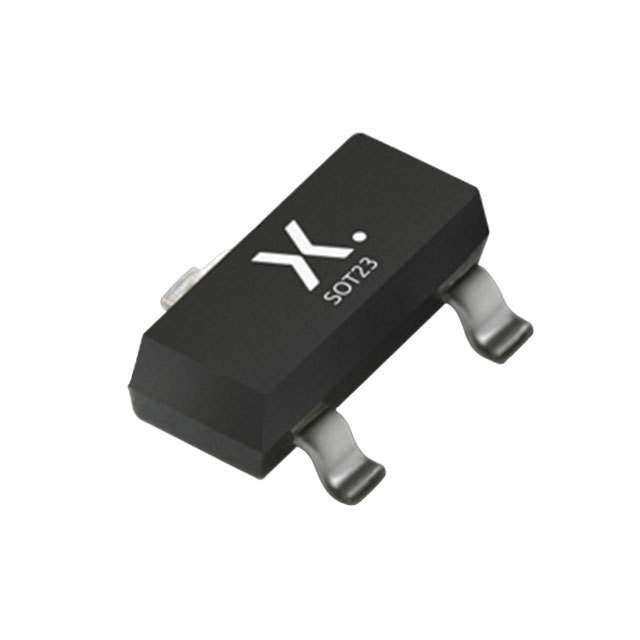
ICGOO电子元器件商城为您提供NX2301P,215由NXP Semiconductors设计生产,在icgoo商城现货销售,并且可以通过原厂、代理商等渠道进行代购。 NX2301P,215价格参考。NXP SemiconductorsNX2301P,215封装/规格:晶体管 - FET,MOSFET - 单, P-Channel 20V 2A (Ta) 400mW (Ta), 2.8W (Tc) Surface Mount TO-236AB。您可以下载NX2301P,215参考资料、Datasheet数据手册功能说明书,资料中有NX2301P,215 详细功能的应用电路图电压和使用方法及教程。
| 参数 | 数值 |
| 产品目录 | |
| 描述 | MOSFET P-CH 20V 2A TO-236ABMOSFET P-CH -20 V -2 A |
| 产品分类 | FET - 单分离式半导体 |
| FET功能 | 逻辑电平门 |
| FET类型 | MOSFET P 通道,金属氧化物 |
| Id-ContinuousDrainCurrent | - 2 A |
| Id-连续漏极电流 | - 2 A |
| 品牌 | NXP Semiconductors |
| 产品手册 | |
| 产品图片 |
|
| rohs | 符合RoHS无铅 / 符合限制有害物质指令(RoHS)规范要求 |
| 产品系列 | 晶体管,MOSFET,NXP Semiconductors NX2301P,215- |
| 数据手册 | |
| 产品型号 | NX2301P,215 |
| PCN封装 | |
| PCN设计/规格 | |
| Pd-PowerDissipation | 400 mW |
| Pd-功率耗散 | 400 mW |
| Qg-GateCharge | 6 nC |
| Qg-栅极电荷 | 6 nC |
| RdsOn-Drain-SourceResistance | 120 mOhms |
| RdsOn-漏源导通电阻 | 120 mOhms |
| Vds-Drain-SourceBreakdownVoltage | - 20 V |
| Vds-漏源极击穿电压 | - 20 V |
| 不同Id时的Vgs(th)(最大值) | 1.1V @ 250µA |
| 不同Vds时的输入电容(Ciss) | 380pF @ 6V |
| 不同Vgs时的栅极电荷(Qg) | 6nC @ 4.5V |
| 不同 Id、Vgs时的 RdsOn(最大值) | 120 毫欧 @ 1A,4.5V |
| 产品种类 | MOSFET |
| 供应商器件封装 | SOT-23 (TO-236AB) |
| 其它名称 | 568-10314-6 |
| 功率-最大值 | 400mW |
| 包装 | Digi-Reel® |
| 商标 | NXP Semiconductors |
| 安装类型 | 表面贴装 |
| 安装风格 | SMD/SMT |
| 封装 | Reel |
| 封装/外壳 | TO-236-3,SC-59,SOT-23-3 |
| 封装/箱体 | SOT-23-3 |
| 工厂包装数量 | 3000 |
| 晶体管极性 | P-Channel |
| 标准包装 | 1 |
| 正向跨导-最小值 | 4.7 S |
| 漏源极电压(Vdss) | 20V |
| 电流-连续漏极(Id)(25°C时) | 2A (Ta) |


- 商务部:美国ITC正式对集成电路等产品启动337调查
- 曝三星4nm工艺存在良率问题 高通将骁龙8 Gen1或转产台积电
- 太阳诱电将投资9.5亿元在常州建新厂生产MLCC 预计2023年完工
- 英特尔发布欧洲新工厂建设计划 深化IDM 2.0 战略
- 台积电先进制程称霸业界 有大客户加持明年业绩稳了
- 达到5530亿美元!SIA预计今年全球半导体销售额将创下新高
- 英特尔拟将自动驾驶子公司Mobileye上市 估值或超500亿美元
- 三星加码芯片和SET,合并消费电子和移动部门,撤换高东真等 CEO
- 三星电子宣布重大人事变动 还合并消费电子和移动部门
- 海关总署:前11个月进口集成电路产品价值2.52万亿元 增长14.8%

PDF Datasheet 数据手册内容提取
NX2301P 20 V, 2 A P-channel Trench MOSFET Rev. 1 — 26 October 2010 Product data sheet 1. Product profile 1.1 General description P-channel enhancement mode Field-Effect Transistor(FET) in a small SOT23(TO-236AB) Surface-Mounted Device(SMD) plastic package using TrenchMOSFET technology. 1.2 Features and benefits (cid:132) 1.8V R rated for Low Voltage Gate Drive DSon (cid:132) Very fast switching (cid:132) Trench MOSFET technology (cid:132) AEC-Q101 qualified 1.3 Applications (cid:132) Relay driver (cid:132) High-speed line driver (cid:132) High-side loadswitch (cid:132) Switching circuits 1.4 Quick reference data Table 1. Quick reference data Symbol Parameter Conditions Min Typ Max Unit V drain-source voltage T =25°C - - −20 V DS amb V gate-source voltage T =25°C - - ±8 V GS amb I drain current T =25°C; [1] - - −2 A D amb V =−4.5V GS R drain-source on-state T =25°C; [2] - 100 120 mΩ DSon j resistance V =−4.5V; GS I =−1A D [1] Device mounted on an FR4PCB, single-sided copper, tin-plated, mounting pad fordrain 6cm2, t≤ 5s. [2] Pulse test: tp≤300μs; δ≤0.01.
NX2301P Nexperia 20 V, 2 A P-channel Trench MOSFET 2. Pinning information Table 2. Pinning Pin Symbol Description Simplified outline Graphic symbol 1 G gate 3 D 2 S source 3 D drain G 1 2 S 017aaa094 3. Ordering information Table 3. Ordering information Type number Package Name Description Version NX2301P TO-236AB plastic surface-mounted package; 3leads SOT23 4. Marking Table 4. Marking codes Type number Marking code[1] NX2301P MG* [1] * = placeholder for manufacturing site code 5. Limiting values Table 5. Limiting values In accordance with the Absolute Maximum Rating System (IEC 60134). Symbol Parameter Conditions Min Max Unit V drain-source voltage T =25°C - −20 V DS amb V gate-source voltage T =25°C - ±8 V GS amb I drain current V =−4.5V [1] D GS T =25°C - −2 A amb T =100°C - −1.2 A amb I peak drain current T =25°C; - −6 A DM amb singlepulse;t ≤10μs p NX2301P All information provided in this document is subject to legal disclaimers. © Nexperia B.V. 2017. All rights reserved Product data sheet Rev. 1 — 26 October 2010 2 of 16
NX2301P Nexperia 20 V, 2 A P-channel Trench MOSFET Table 5. Limiting values …continued In accordance with the Absolute Maximum Rating System (IEC 60134). Symbol Parameter Conditions Min Max Unit P total power dissipation T =25°C [2] - 400 mW tot amb [1] - 710 mW T =25°C - 2.8 W sp T junction temperature 150 °C j T ambient temperature −55 +150 °C amb T storage temperature −65 +150 °C stg Source-drain diode I source current T =25°C [1] - −0.7 A S amb [1] Device mounted on an FR4PCB, single-sided copper, tin-plated, mounting pad fordrain 6cm2, t≤ 5s. [2] Device mounted on an FR4PCB, single-sided copper, tin-plated and standard footprint. 017aaa001 017aaa002 120 120 Pder Ider (%) (%) 80 80 40 40 0 0 −75 −25 25 75 125 175 −75 −25 25 75 125 175 Tamb (°C) Tamb (°C) P I P = ------------t-o---t--------×100% I = ----------D----------×100% der P der I tot(25°C) D(25°C) Fig 1. Normalized total power dissipation as a Fig 2. Normalized continuous drain current as a function of ambient temperature function of ambient temperature NX2301P All information provided in this document is subject to legal disclaimers. © Nexperia B.V. 2017. All rights reserved Product data sheet Rev. 1 — 26 October 2010 3 of 16
NX2301P Nexperia 20 V, 2 A P-channel Trench MOSFET −10 017aaa095 Limit RDSon = VDS/ID ID (A) (1) −1 (2) (3) −10−1 (4) (5) −10−2 −10−1 −1 −10 −102 VDS (V) I =single pulse DM (1) tp=1ms (2) tp=10ms (3) DC; Tsp=25°C (4) tp=100ms (5) DC; Tamb=25°C; drain mounting pad 6cm2 Fig 3. Safe operating area; junction to ambient; continuous and peak drain currents as a function of drain-source voltage 6. Thermal characteristics Table 6. Thermal characteristics Symbol Parameter Conditions Min Typ Max Unit R thermal resistance from in free air [1] - - 315 K/W th(j-a) junction to ambient [2] - - 175 K/W R thermal resistance from - - 45 K/W th(j-sp) junction to solder point [1] Device mounted on an FR4PCB, single-sided copper, tin-plated and standard footprint. [2] Device mounted on an FR4PCB, single-sided copper, tin-plated, mounting pad fordrain 6cm2, t≤ 5s. NX2301P All information provided in this document is subject to legal disclaimers. © Nexperia B.V. 2017. All rights reserved Product data sheet Rev. 1 — 26 October 2010 4 of 16
NX2301P Nexperia 20 V, 2 A P-channel Trench MOSFET 103 017aaa096 Zth(j-a) duty cycle = 1 (K/W) 0.75 0.5 102 0.33 0.25 0.2 0.1 0.05 10 0.02 0.01 0 1 10−3 10−2 10−1 1 10 102 103 tp (s) FR4PCB, standard footprint Fig 4. Transient thermal impedance from junction to ambient as a function of pulse duration; typical values 103 017aaa097 Zth(j-a) (K/W) duty cycle = 1 0.75 102 0.5 0.33 0.25 0.2 0.1 0.05 10 0 0.02 0.01 1 10−3 10−2 10−1 1 10 102 103 tp (s) FR4PCB, mounting pad for drain 6cm2 Fig 5. Transient thermal impedance from junction to ambient as a function of pulse duration; typical values NX2301P All information provided in this document is subject to legal disclaimers. © Nexperia B.V. 2017. All rights reserved Product data sheet Rev. 1 — 26 October 2010 5 of 16
NX2301P Nexperia 20 V, 2 A P-channel Trench MOSFET 7. Characteristics Table 7. Characteristics T =25°C unless otherwise specified. j Symbol Parameter Conditions Min Typ Max Unit Static characteristics V drain-source breakdown I =−250μA; V =0V −20 - - V (BR)DSS D GS voltage V gate-source threshold I =−250μA; V =V −0.5 −0.75 −1.1 V GS(th) D DS GS voltage I drain leakage current V =−20V; V =0V - - −1 μA DSS DS GS I gate leakage current V =±8V; V =0V - - ±100 nA GSS GS DS R drain-source on-state [1] DSon resistance V =−4.5V; I =−1A GS D T =25°C 100 120 mΩ j T =150°C - 180 mΩ j V =−2.5V; I =−1A - 155 190 mΩ GS D V =−1.8V; - 210 270 mΩ GS I =−0.2A D g forward V =−5V; I =−2A [1] - 4.7 - S fs DS D transconductance Dynamic characteristics Q total gate charge I =−2.2A; V =−6V; - 4.5 6 nC G(tot) D DS V =−4.5V Q gate-source charge GS - 1.1 - nC GS Q gate-drain charge - 0.9 - nC GD C input capacitance V =0V; V =−6V; - 380 - pF iss GS DS f=1MHz C output capacitance - 135 - pF oss C reverse transfer - 115 - pF rss capacitance t turn-on delay time V =−6V; - 7 - ns d(on) DD R =6Ω; t rise time L - 15 - ns r V =−4.5V; GS td(off) turn-off delay time RG=6Ω - 50 - ns t fall time - 25 - ns f Source-drain diode V source-drain voltage I =−1A; V =0V [1] - −0.8 −1.0 V SD S GS [1] Pulse test: tp≤300μs; δ≤0.01. NX2301P All information provided in this document is subject to legal disclaimers. © Nexperia B.V. 2017. All rights reserved Product data sheet Rev. 1 — 26 October 2010 6 of 16
NX2301P Nexperia 20 V, 2 A P-channel Trench MOSFET −3.0 017aaa098 −10−3 017aaa099 VGS = −2.0 V −1.8 V ID ID (A) (A) −2.0 −10−4 −1.6 V (1) (2) (3) −1.0 −10−5 −1.4 V −1.2 V 0.0 −10−6 0.0 −1.0 −2.0 −3.0 −4.0 −5.0 0.0 −0.5 −1.0 −1.5 VDS (V) VGS (V) Tamb=25°C Tamb=25°C; VDS=−10V (1) minimum values (2) typical values (3) maximum values Fig 6. Output characteristics: drain current as a Fig 7. Sub-threshold drain current as a function of function of drain-source voltage; typical gate-source voltage values 017aaa100 017aaa101 1.0 0.4 RDSon RDson (Ω) (Ω) (1) (2) 0.75 0.3 0.50 0.2 (3) (1) 0.25 0.1 (4) (2) 0.0 0.0 0.0 −0.5 −1.0 −1.5 −2.0 −2.5 0.0 −2.0 −4.0 −6.0 −8.0 ID (A) VGS (V) Tamb=25°C ID=−2A (1) VGS=−1.4V (1) Tamb=125°C (2) VGS=−1.6V (2) Tamb=25°C (3) VGS=−1.8V (4) VGS=−2.0V Fig 8. Drain-source on-state resistance as a function Fig 9. Drain-source on-state resistance as a function of drain current; typical values of gate-source voltage; typical values NX2301P All information provided in this document is subject to legal disclaimers. © Nexperia B.V. 2017. All rights reserved Product data sheet Rev. 1 — 26 October 2010 7 of 16
NX2301P Nexperia 20 V, 2 A P-channel Trench MOSFET −2.0 017aaa102 2.0 017aaa103 ID a (A) −1.5 1.5 (1) (2) −1.0 1.0 −0.5 0.5 0.0 0.0 0.0 −1.0 −2.0 −3.0 −60 0 60 120 180 VGS (V) Tamb (°C) VDS>ID×RDSon R a = ------------D---S---o---n-------- (1) Tamb=150°C R DSon(25°C) (2) Tamb=25°C Fig 10. Transfer characteristics: drain current as a Fig 11. Normalized drain-source on-state resistance function of gate-source voltage; typical values as a function of ambient temperature; typical values −1.5 017aaa104 103 017aaa105 VGS(th) (1) (V) C (pF) −1.0 (1) (2) 102 (3) (2) −0.5 (3) 0.0 10 −60 0 60 120 180 −10−1 −1 −10 −102 Tamb (°C) VDS (V) ID=−0.25mA; VDS=VGS f=1MHz; VGS=0V (1) maximum values (1) Ciss (2) typical values (2) Coss (3) minimum values (3) Crss Fig 12. Gate-source threshold voltage as a function of Fig 13. Input, output and reverse transfer ambient temperature capacitances as a function of drain-source voltage; typical values NX2301P All information provided in this document is subject to legal disclaimers. © Nexperia B.V. 2017. All rights reserved Product data sheet Rev. 1 — 26 October 2010 8 of 16
NX2301P Nexperia 20 V, 2 A P-channel Trench MOSFET −5.0 017aaa106 VGS (V) −4.0 VDS −3.0 ID VGS(pl) −2.0 VGS(th) −1.0 VGS QGS1 QGS2 QGS QGD 0.00.0 1.25 2.5 3.75 5.0 QG(tot) QG (nC) 003aaa508 ID=−2A; VDS=−6V; Tamb=25°C Fig 14. Gate-source voltage as a function of gate Fig 15. Gate charge waveform definitions charge; typical values −1.0 017aaa107 IS (A) −0.75 (1) (2) −0.5 −0.25 0.0 0.0 −0.25 −0.5 −0.75 −1.0 VSD (V) V =0V GS (1) Tamb=150°C (2) Tamb=25°C Fig 16. Source current as a function of source-drain voltage; typical values NX2301P All information provided in this document is subject to legal disclaimers. © Nexperia B.V. 2017. All rights reserved Product data sheet Rev. 1 — 26 October 2010 9 of 16
NX2301P Nexperia 20 V, 2 A P-channel Trench MOSFET 8. Test information P duty cycle δ = t1 t2 t2 t1 t 006aaa812 Fig 17. Duty cycle definition 8.1 Quality information This product has been qualified in accordance with the Automotive Electronics Council (AEC) standard Q101 - Stress test qualification for discrete semiconductors, and is suitable for use in automotive applications. NX2301P All information provided in this document is subject to legal disclaimers. © Nexperia B.V. 2017. All rights reserved Product data sheet Rev. 1 — 26 October 2010 10 of 16
NX2301P Nexperia 20 V, 2 A P-channel Trench MOSFET 9. Package outline Plastic surface-mounted package; 3 leads SOT23 D B E A X HE v M A 3 Q A A1 1 2 c e1 bp w M B Lp e detail X 0 1 2 mm scale DIMENSIONS (mm are the original dimensions) UNIT A mAa1x. bp c D E e e1 HE Lp Q v w 1.1 0.48 0.15 3.0 1.4 2.5 0.45 0.55 mm 0.1 1.9 0.95 0.2 0.1 0.9 0.38 0.09 2.8 1.2 2.1 0.15 0.45 OUTLINE REFERENCES EUROPEAN ISSUE DATE VERSION IEC JEDEC JEITA PROJECTION 04-11-04 SOT23 TO-236AB 06-03-16 Fig 18. Package outline SOT23(TO-236AB) NX2301P All information provided in this document is subject to legal disclaimers. © Nexperia B.V. 2017. All rights reserved Product data sheet Rev. 1 — 26 October 2010 11 of 16
NX2301P Nexperia 20 V, 2 A P-channel Trench MOSFET 10. Soldering 3.3 2.9 1.9 solder lands solder resist 3 1.7 2 solder paste 0.7 0.6 occupied area (3×) (3×) Dimensions in mm 0.5 (3×) 0.6 (3×) 1 sot023_fr Fig 19. Reflow soldering footprint SOT23(TO-236AB) 2.2 1.2 (2×) 1.4 (2×) solder lands 4.6 2.6 solder resist occupied area Dimensions in mm 1.4 preferred transport direction during soldering 2.8 4.5 sot023_fw Fig 20. Wave soldering footprint SOT23(TO-236AB) NX2301P All information provided in this document is subject to legal disclaimers. © Nexperia B.V. 2017. All rights reserved Product data sheet Rev. 1 — 26 October 2010 12 of 16
NX2301P Nexperia 20 V, 2 A P-channel Trench MOSFET 11. Revision history Table 8. Revision history Document ID Release date Data sheet status Change notice Supersedes NX2301P v.1 20101026 Product data sheet - - NX2301P All information provided in this document is subject to legal disclaimers. © Nexperia B.V. 2017. All rights reserved Product data sheet Rev. 1 — 26 October 2010 13 of 16
NX2301P Nexperia 20 V, 2 A P-channel Trench MOSFET 12. Legal information 12.1 Data sheet status Document status[1][2] Product status[3] Definition Objective [short] data sheet Development This document contains data from the objective specification for product development. Preliminary [short] data sheet Qualification This document contains data from the preliminary specification. Product [short] data sheet Production This document contains the product specification. [1] Please consult the most recently issued document before initiating or completing a design. [2] The term ‘short data sheet’ is explained in section “Definitions”. [3] The product status of device(s) described in this document may have changed since this document was published and may differ in case of multiple devices. The latest product status information is available on the Internet at URLhttp://www.nexperia.com. 12.2 Definitions malfunction of a Nexperia product can reasonably be expected to result in personal injury, death or severe property or environmental damage. Nexperia accepts no liability for inclusion and/or use of Draft — The document is a draft version only. The content is still under Nexperia products in such equipment or applications and internal review and subject to formal approval, which may result in therefore such inclusion and/or use is at the customer’s own risk. modifications or additions. Nexperia does not give any representations or warranties as to the accuracy or completeness of Applications — Applications that are described herein for any of these information included herein and shall have no liability for the consequences of products are for illustrative purposes only. Nexperia makes no use of such information. representation or warranty that such applications will be suitable for the specified use without further testing or modification. Short data sheet — A short data sheet is an extract from a full data sheet with the same product type number(s) and title. A short data sheet is intended Customers are responsible for the design and operation of their applications for quick reference only and should not be relied upon to contain detailed and and products using Nexperia products, and Nexperia full information. For detailed and full information see the relevant full data accepts no liability for any assistance with applications or customer product sheet, which is available on request via the local Nexperia sales design. It is customer’s sole responsibility to determine whether the Nexperia office. In case of any inconsistency or conflict with the short data sheet, the product is suitable and fit for the customer’s applications and full data sheet shall prevail. products planned, as well as for the planned application and use of customer’s third party customer(s). Customers should provide appropriate Product specification — The information and data provided in a Product design and operating safeguards to minimize the risks associated with their data sheet shall define the specification of the product as agreed between applications and products. Nexperia and its customer, unless Nexperia and Nexperia does not accept any liability related to any default, customer have explicitly agreed otherwise in writing. In no event however, damage, costs or problem which is based on any weakness or default in the shall an agreement be valid in which the Nexperia product is customer’s applications or products, or the application or use by customer’s deemed to offer functions and qualities beyond those described in the third party customer(s). Customer is responsible for doing all necessary Product data sheet. testing for the customer’s applications and products using Nexperia products in order to avoid a default of the applications and 12.3 Disclaimers the products or of the application or use by customer’s third party customer(s). Nexperia does not accept any liability in this respect. Limited warranty and liability — Information in this document is believed to Limiting values — Stress above one or more limiting values (as defined in be accurate and reliable. However, Nexperia does not give any the Absolute Maximum Ratings System of IEC60134) will cause permanent representations or warranties, expressed or implied, as to the accuracy or damage to the device. Limiting values are stress ratings only and (proper) completeness of such information and shall have no liability for the operation of the device at these or any other conditions above those given in consequences of use of such information. the Recommended operating conditions section (if present) or the Characteristics sections of this document is not warranted. Constant or In no event shall Nexperia be liable for any indirect, incidental, repeated exposure to limiting values will permanently and irreversibly affect punitive, special or consequential damages (including - without limitation - lost the quality and reliability of the device. profits, lost savings, business interruption, costs related to the removal or replacement of any products or rework charges) whether or not such Terms and conditions of commercial sale — Nexperia damages are based on tort (including negligence), warranty, breach of products are sold subject to the general terms and conditions of commercial contract or any other legal theory. sale, as published at http://www.nexperia.com/profile/terms, unless otherwise Notwithstanding any damages that customer might incur for any reason agreed in a valid written individual agreement. In case an individual whatsoever, Nexperia’s aggregate and cumulative liability towards agreement is concluded only the terms and conditions of the respective customer for the products described herein shall be limited in accordance agreement shall apply. Nexperia hereby expressly objects to with the Terms and conditions of commercial sale of Nexperia. applying the customer’s general terms and conditions with regard to the purchase of Nexperia products by customer. Right to make changes — Nexperia reserves the right to make changes to information published in this document, including without No offer to sell or license — Nothing in this document may be interpreted or limitation specifications and product descriptions, at any time and without construed as an offer to sell products that is open for acceptance or the grant, notice. This document supersedes and replaces all information supplied prior conveyance or implication of any license under any copyrights, patents or to the publication hereof. other industrial or intellectual property rights. Suitability for use — Nexperia products are not designed, Export control — This document as well as the item(s) described herein authorized or warranted to be suitable for use in life support, life-critical or may be subject to export control regulations. Export might require a prior safety-critical systems or equipment, nor in applications where failure or authorization from national authorities. NX2301P All information provided in this document is subject to legal disclaimers. © Nexperia B.V. 2017. All rights reserved Product data sheet Rev. 1 — 26 October 2010 14 of 16
NX2301P Nexperia 20 V, 2 A P-channel Trench MOSFET Quick reference data — The Quick reference data is an extract of the 12.4 Trademarks product data given in the Limiting values and Characteristics sections of this document, and as such is not complete, exhaustive or legally binding. Notice: All referenced brands, product names, service names and trademarks are the property of their respective owners. 13. Contact information For more information, please visit: http://www.nexperia.com For sales office addresses, please send an email to: salesaddresses@nexperia.com NX2301P All information provided in this document is subject to legal disclaimers. © Nexperia B.V. 2017. All rights reserved Product data sheet Rev. 1 — 26 October 2010 15 of 16
NX2301P Nexperia 20 V, 2 A P-channel Trench MOSFET 14. Contents 1 Product profile. . . . . . . . . . . . . . . . . . . . . . . . . . 1 1.1 General description . . . . . . . . . . . . . . . . . . . . . 1 1.2 Features and benefits. . . . . . . . . . . . . . . . . . . . 1 1.3 Applications . . . . . . . . . . . . . . . . . . . . . . . . . . . 1 1.4 Quick reference data . . . . . . . . . . . . . . . . . . . . 1 2 Pinning information. . . . . . . . . . . . . . . . . . . . . . 2 3 Ordering information. . . . . . . . . . . . . . . . . . . . . 2 4 Marking. . . . . . . . . . . . . . . . . . . . . . . . . . . . . . . . 2 5 Limiting values. . . . . . . . . . . . . . . . . . . . . . . . . . 2 6 Thermal characteristics . . . . . . . . . . . . . . . . . . 4 7 Characteristics. . . . . . . . . . . . . . . . . . . . . . . . . . 6 8 Test information. . . . . . . . . . . . . . . . . . . . . . . . 10 8.1 Quality information . . . . . . . . . . . . . . . . . . . . . 10 9 Package outline. . . . . . . . . . . . . . . . . . . . . . . . 11 10 Soldering . . . . . . . . . . . . . . . . . . . . . . . . . . . . . 12 11 Revision history. . . . . . . . . . . . . . . . . . . . . . . . 13 12 Legal information. . . . . . . . . . . . . . . . . . . . . . . 14 12.1 Data sheet status . . . . . . . . . . . . . . . . . . . . . . 14 12.2 Definitions. . . . . . . . . . . . . . . . . . . . . . . . . . . . 14 12.3 Disclaimers. . . . . . . . . . . . . . . . . . . . . . . . . . . 14 12.4 Trademarks. . . . . . . . . . . . . . . . . . . . . . . . . . . 15 13 Contact information. . . . . . . . . . . . . . . . . . . . . 15 14 Contents. . . . . . . . . . . . . . . . . . . . . . . . . . . . . . 16 © Nexperia B.V. 2017. All rights reserved For more information, please visit: http://www.nexperia.com For sales office addresses, please send an email to: salesaddresses@nexperia.com Date of release: 26 October 2010