ICGOO在线商城 > 分立半导体产品 > 晶体管 - FET,MOSFET - 单 > NVD5117PLT4G
 Datasheet下载
- 型号: NVD5117PLT4G
- 制造商: ON Semiconductor
- 库位|库存: xxxx|xxxx
- 要求:
| 数量阶梯 | 香港交货 | 国内含税 |
| +xxxx | $xxxx | ¥xxxx |
查看当月历史价格
查看今年历史价格
NVD5117PLT4G产品简介:
ICGOO电子元器件商城为您提供NVD5117PLT4G由ON Semiconductor设计生产,在icgoo商城现货销售,并且可以通过原厂、代理商等渠道进行代购。 NVD5117PLT4G价格参考。ON SemiconductorNVD5117PLT4G封装/规格:晶体管 - FET,MOSFET - 单, P-Channel 60V 11A (Ta), 61A (Tc) 4.1W (Ta), 118W (Tc) Surface Mount DPAK。您可以下载NVD5117PLT4G参考资料、Datasheet数据手册功能说明书,资料中有NVD5117PLT4G 详细功能的应用电路图电压和使用方法及教程。
| 参数 | 数值 |
| 产品目录 | |
| 描述 | MOSFET P-CH 60V 61A DPAKMOSFET 60V T1 PCH DPAK |
| 产品分类 | FET - 单分离式半导体 |
| FET功能 | 逻辑电平门 |
| FET类型 | MOSFET P 通道,金属氧化物 |
| Id-ContinuousDrainCurrent | - 61 A |
| Id-连续漏极电流 | - 61 A |
| 品牌 | ON Semiconductor |
| 产品手册 | |
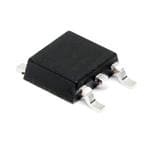
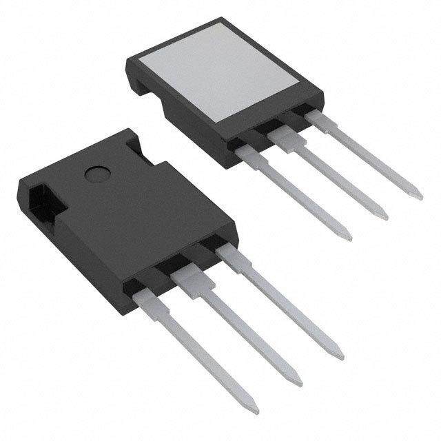
| 产品图片 |
|
| rohs | 符合RoHS无铅 / 符合限制有害物质指令(RoHS)规范要求 |
| 产品系列 | 晶体管,MOSFET,ON Semiconductor NVD5117PLT4G- |
| 数据手册 | |
| 产品型号 | NVD5117PLT4G |
| Pd-PowerDissipation | 118 W |
| Pd-功率耗散 | 118 W |
| Qg-GateCharge | 85 nC |
| Qg-栅极电荷 | 85 nC |
| RdsOn-Drain-SourceResistance | 16 mOhms |
| RdsOn-漏源导通电阻 | 16 mOhms |
| Vds-Drain-SourceBreakdownVoltage | - 60 V |
| Vds-漏源极击穿电压 | - 60 V |
| Vgs-Gate-SourceBreakdownVoltage | +/- 20 V |
| Vgs-栅源极击穿电压 | 20 V |
| 上升时间 | 195 ns |
| 下降时间 | 132 ns |
| 不同Id时的Vgs(th)(最大值) | 2.5V @ 250µA |
| 不同Vds时的输入电容(Ciss) | 4800pF @ 25V |
| 不同Vgs时的栅极电荷(Qg) | 85nC @ 10V |
| 不同 Id、Vgs时的 RdsOn(最大值) | 16 毫欧 @ 29A,10V |
| 产品种类 | MOSFET |
| 供应商器件封装 | DPAK-3 |
| 其它名称 | NVD5117PLT4GOSCT |
| 典型关闭延迟时间 | 50 ns |
| 功率-最大值 | 4.1W |
| 功率耗散 | 118 W |
| 包装 | 剪切带 (CT) |
| 商标 | ON Semiconductor |
| 安装类型 | 表面贴装 |
| 安装风格 | SMD/SMT |
| 导通电阻 | 16 mOhms |
| 封装 | Reel |
| 封装/外壳 | TO-252-3,DPak(2 引线+接片),SC-63 |
| 封装/箱体 | DPAK-4 |
| 工厂包装数量 | 2500 |
| 晶体管极性 | P-Channel |
| 最大工作温度 | + 175 C |
| 最小工作温度 | - 55 C |
| 栅极电荷Qg | 85 nC |
| 标准包装 | 1 |
| 汲极/源极击穿电压 | - 60 V |
| 漏极连续电流 | - 61 A |
| 漏源极电压(Vdss) | 60V |
| 电流-连续漏极(Id)(25°C时) | 11A (Ta), 61A (Tc) |
| 系列 | NVD5117PL |
| 配置 | Single |
| 闸/源击穿电压 | +/- 20 V |


PDF Datasheet 数据手册内容提取
NVD5117PL Power MOSFET (cid:2) −60 V, 16 m , −61 A, Single P−Channel Features • Low R to Minimize Conduction Losses DS(on) • High Current Capability • www.onsemi.com Avalanche Energy Specified • AEC−Q101 Qualified • These Devices are Pb−Free, Halogen Free/BFR Free and are RoHS V(BR)DSS RDS(on) ID Compliant 16 m(cid:4) @ −10 V −60 V −61 A 22 m(cid:4) @ −4.5 V MAXIMUM RATINGS (TJ = 25°C unless otherwise noted) S Parameter Symbol Value Unit Drain−to−Source Voltage VDSS −60 V G Gate−to−Source Voltage VGS (cid:2)20 V P−Channel Continuous Drain Cur- TC = 25°C ID −61 A rent R(cid:2)JC (Note 1) Steady TC = 100°C −43 D Power Dissipation R(cid:2)JC State TC = 25°C PD 118 W (Note 1) 4 TC = 100°C 59 Creonnt tRin(cid:2)uJoAu (sN Dotreasin 1 C &u r2-) Steady TTAA = = 1 2050°°CC ID −−181 A 1 2 3 Power Dissipation R(cid:2)JA State TA = 25°C PD 4.1 W CADSPEA 3K69C (Notes 1 & 2) TA = 100°C 2.1 STYLE 2 Pulsed Drain Current TA = 25°C, tp = 10 (cid:3)s IDM −419 A MARKING DIAGRAMS Current Limited by TA = 25°C IDmaxpkg 60 A & PIN AS4SIGNMENT Package (Note 3) Drain Operating Junction and Storage Temperature TJ, Tstg −55 to °C 175 W W G L Source Current (Body Diode) IS −118 A AY5117 Single Pulse Drain−to−Source Avalanche EAS 240 mJ Energy (TJ = 25°C, VDD = 50 V, VGS = 10 V, 2 IL(pk) = 40 A, L = 0.3 mH, RG = 25 (cid:4)) 1Drain 3 Gate Source Lead Temperature for Soldering Purposes TL 260 °C A = Assembly Location* (1/8″ from case for 10 s) Y = Year Stresses exceeding those listed in the Maximum Ratings table may damage the WW = Work Week device. If any of these limits are exceeded, device functionality should not be 5117L = Device Code assumed, damage may occur and reliability may be affected. G = Pb−Free Package THERMAL RESISTANCE MAXIMUM RATINGS * The Assembly Location Code (A) is front side Parameter Symbol Value Unit optional. In cases where the Assembly Location is stamped in the package bottom (molding ejecter Junction−to−Case − Steady State (Drain) R(cid:2)JC 1.3 °C/W pin), the front side assembly code may be blank. Junction−to−Ambient − Steady State (Note 2) R(cid:2)JA 37 ORDERING INFORMATION 1. The entire application environment impacts the thermal resistance values shown, they are not constants and are only valid for the particular conditions Device Package Shipping† noted. 2. Surface−mounted on FR4 board using a 650 mm2, 2 oz. Cu pad. NVD5117PLT4G DPAK 22550000 // TTaappee && 3. Maximum current for pulses as long as 1 second is higher but is dependent (Pb−Free) RReeeell on pulse duration and duty cycle. NVD5117PLT4G− DPAK 2500 / Tape & VF01 (Pb−Free) Reel †For information on tape and reel specifications, including part orientation and tape sizes, please refer to our Tape and Reel Packaging Specifications Brochure, BRD8011/D. © Semiconductor Components Industries, LLC, 2017 1 Publication Order Number: May, 2017 − Rev. 2 NVD5117PL/D
NVD5117PL ELECTRICAL CHARACTERISTICS (TJ = 25°C unless otherwise noted) Parameter Symbol Test Condition Min Typ Max Unit OFF CHARACTERISTICS Drain−to−Source Breakdown Voltage V(BR)DSS VGS = 0 V, ID = −250 (cid:3)A −60 V Zero Gate Voltage Drain Current IDSS VGS = 0 V, TJ = 25°C −1.0 (cid:3)A VDS = −60 V TJ = 125°C −100 Gate−to−Source Leakage Current IGSS VDS = 0 V, VGS = (cid:2)20 V (cid:2)100 nA ON CHARACTERISTICS (Note 4) Gate Threshold Voltage VGS(TH) VGS = VDS, ID = −250 (cid:3)A −1.5 −2.5 V Drain−to−Source On Resistance RDS(on) VGS = −10 V, ID = −29 A 12 16 m(cid:4) VGS = −4.5 V, ID = −29 A 16 22 Froward Transconductance gFS VDS = −15 V, ID = −15 A 30 S CHARGES AND CAPACITANCES Input Capacitance Ciss VGS = 0 V, f = 1.0 MHz, 4800 pF VDS = −25 V Output Capacitance Coss 480 Reverse Transfer Capacitance Crss 320 Total Gate Charge QG(TOT) VDS = −48 V, VGS = −4.5 V 49 nC ID = −29 A VGS = −10 V 85 Threshold Gate Charge QG(TH) 3 Gate−to−Source Charge QGS VGS = −4.5 V, VDS = −48 V, 13 Gate−to−Drain Charge QGD ID = −29 A 28 Plateau Voltage VGP 3.2 V SWITCHING CHARACTERISTICS (Notes 4) Turn−On Delay Time td(on) 22 ns Rise Time tr VGS = −4.5 V, VDS = −48 V, 195 Turn−Off Delay Time td(off) ID = −29 A, RG = 2.5 (cid:4) 50 Fall Time tf 132 DRAIN−SOURCE DIODE CHARACTERISTICS Forward Diode Voltage VSD VGS = 0 V, TJ = 25°C −0.86 −1.0 V IS = −29 A TJ = 125°C −0.74 Reverse Recovery Time tRR 36 ns Charge Time ta VGS = 0 V, dls/dt = 100 A/(cid:3)s, 19 Discharge Time tb Is = −29 A 17 Reverse Recovery Charge QRR 44 nC Product parametric performance is indicated in the Electrical Characteristics for the listed test conditions, unless otherwise noted. Product performance may not be indicated by the Electrical Characteristics if operated under different conditions. 4. Pulse Test: Pulse Width ≤ 300 (cid:3)s, Duty Cycle ≤ 2%. www.onsemi.com 2
NVD5117PL TYPICAL CHARACTERISTICS 120 120 VGS = −10 V −4.5 V −4.2 V TJ = 25°C VDS ≥ −10 V A) 100 A) 100 T ( −4 V T ( EN 80 EN 80 R −3.8 V R R R U U C 60 −3.6 V C 60 N N RAI 40 −3.4 V RAI 40 D D , D −3.2 V , D TJ = 25°C −I 20 −3 V −I 20 TJ = 125°C TJ = −55°C 0 0 0 1 2 3 4 5 2 3 4 5 6 −VDS, DRAIN−TO−SOURCE VOLTAGE (V) −VGS, GATE−TO−SOURCE VOLTAGE (V) Figure 1. On−Region Characteristics Figure 2. Transfer Characteristics (cid:4)CE () (cid:4)E () 0.024 AN 0.065 ID = −29 A NC TJ = 25°C ST TJ = 25°C TA 0.022 RESI 0.055 ESIS 0.020 VGS = −4.5 V CE 0.045 E R R C 0.018 U R SO 0.035 OU 0.016 − S O − −T 0.025 TO 0.014 N − DRAI 0.015 RAIN 0.012 VGS = −10 V , DS(on)0.0053 4 5 6 7 8 9 10, DS(on)0.01010 20 30 40 50 60 70 80 90 100 110 120 R D R −VGS, GATE−TO−SOURCE VOLTAGE (V) −ID, DRAIN CURRENT (A) Figure 3. On−Resistance vs. Gate−to−Source Figure 4. On−Resistance vs. Drain Current and D) Voltage Gate Voltage E Z LI A 2.00 100000 M R VGS = −10 V VGS = 0 V NO 1.80 ID = −29 A CE ( 1.60 A) TJ = 150°C TAN E (n10000 S 1.40 G RESI 1.20 EAKA TJ = 125°C E L URC 1.00 , DSS 1000 O −I S − 0.80 O T − N 0.60 100 AI −50 −25 0 25 50 75 100 125 150 175 5 10 15 20 25 30 35 40 45 50 55 60 R , Dn) TJ, JUNCTION TEMPERATURE (°C) −VDS, DRAIN−TO−SOURCE VOLTAGE (V) S(o Figure 5. On−Resistance Variation with Figure 6. Drain−to−Source Leakage Current RD Temperature vs. Voltage www.onsemi.com 3
NVD5117PL TYPICAL CHARACTERISTICS 6000 10 V) 55050000 VTJG S= =2 50° CV GE ( QT A 8 F) 4500 Ciss LT p O CE ( 34500000 CE V 6 N R TA 3000 U CAPACI 22050000 −TO−SO 4 Qgs Qgd C, 11050000 ATE 2 VDS = −48 V 500 Crss Coss , GGS ITDJ == −2259° CA 0 V 0 0 10 20 30 40 50 60− 0 10 20 30 40 50 60 70 80 90 −VDS, DRAIN−TO−SOURCE VOLTAGE (V) Qg, TOTAL GATE CHARGE (nC) Figure 7. Capacitance Variation Figure 8. Gate−to−Source vs. Total Charge 1000.0 120 VGS = 0 V A) 100 TJ = 25°C tr td(off) NT ( s)100.0 tf RE 80 n R E ( CU 60 TIM td(on) CE t, 10.0 UR 40 O S VDD = −48 V , S 20 ID = −29 A I VGS = −10 V 1.0 0 1 10 100 0.4 0.5 0.6 0.7 0.8 0.9 1.0 1.1 1.2 RG, GATE RESISTANCE ((cid:4)) −VSD, SOURCE−TO−DRAIN VOLTAGE (V) Figure 9. Resistive Switching Time Variation Figure 10. Diode Forward Voltage vs. Current vs. Gate Resistance 1000 250 VGS = −10 V 100 (cid:3)s 10 (cid:3)s −mJ) ID = −40 A T (A) 100 STCin g=l e2 5P°uClse 10 m1s ms AIN−TOERGY (200 N RN RRE E DE E150 N CU 10 dc PULSANCH100 AI E L R LA −I, DD 1 RThDeSr(mona) lL Limimitit , SINGSRCE AV 50 AU Package Limit EO 0.1 S 0 0.1 1 10 100 25 50 75 100 125 150 175 −VDS, DRAIN−TO−SOURCE VOLTAGE (V) TJ, STARTING JUNCTION TEMPERATURE (°C) Figure 11. Maximum Rated Forward Biased Figure 12. Maximum Avalanche Energy vs. Safe Operating Area Starting Junction Temperature www.onsemi.com 4
NVD5117PL TYPICAL CHARACTERISTICS 10 T N E SI NE AC RN E TTA 1 Duty Cycle = 0.5 VS TISI CE 0.2 ER W) EFFRMAL 0.1 0.00.51 C/HE 0.02 ° (C(t)T (cid:2)J 0.01 Single Pulse R 0.01 0.000001 0.00001 0.0001 0.001 0.01 0.1 PULSE TIME (sec) Figure 13. Thermal Response www.onsemi.com 5
NVD5117PL PACKAGE DIMENSIONS DPAK (SINGLE GAUGE) CASE 369C ISSUE F NOTES: A 1.DIMENSIONING AND TOLERANCING PER ASME Y14.5M, 1994. E C 2.CONTROLLING DIMENSION: INCHES. A 3.THERMAL PAD CONTOUR OPTIONAL WITHIN DI- b3 B MENSIONS b3, L3 and Z. c2 4.DIMENSIONS D AND E DO NOT INCLUDE MOLD FLASH, PROTRUSIONS, OR BURRS. MOLD FLASH, PROTRUSIONS, OR GATE BURRS SHALL 4 NOT EXCEED 0.006 INCHES PER SIDE. L3 Z 5.DIMENSIONS D AND E ARE DETERMINED AT THE D DETAIL A H 6.DOAUTTUEMRSM OA SATN EDX BT RAERME EDSE OTEFR TMHIEN EPDLA ASTT DICA TBUOMDY. 1 2 3 PLANE H. 7.OPTIONAL MOLD FEATURE. L4 INCHES MILLIMETERS NOTE 7 b2 c BOTTOM VIEW DIM MIN MAX MIN MAX A 0.086 0.094 2.18 2.38 e SIDE VIEW A1 0.000 0.005 0.00 0.13 b b 0.025 0.035 0.63 0.89 0.005 (0.13) M C b2 0.028 0.045 0.72 1.14 TOP VIEW b3 0.180 0.215 4.57 5.46 c 0.018 0.024 0.46 0.61 c2 0.018 0.024 0.46 0.61 H Z Z D 0.235 0.245 5.97 6.22 E 0.250 0.265 6.35 6.73 e 0.090 BSC 2.29 BSC L2 GPLAAUNGEE C SPELAATNIENG H 0.370 0.410 9.40 10.41 L 0.055 0.070 1.40 1.78 L1 0.114 REF 2.90 REF L2 0.020 BSC 0.51 BSC L A1 BOTTOM VIEW L3 0.035 0.050 0.89 1.27 L1 ALTERNATE L4 −−− 0.040 −−− 1.01 CONSTRUCTIONS Z 0.155 −−− 3.93 −−− DETAIL A ROTATED 90(cid:2) CW SOLDERING FOOTPRINT* 6.20 3.00 0.244 0.118 2.58 0.102 5.80 1.60 6.17 0.228 0.063 0.243 (cid:3) (cid:4) mm SCALE 3:1 inches *For additional information on our Pb−Free strategy and soldering details, please download the ON Semiconductor Soldering and Mounting Techniques Reference Manual, SOLDERRM/D. ON Semiconductor and are trademarks of Semiconductor Components Industries, LLC dba ON Semiconductor or its subsidiaries in the United States and/or other countries. ON Semiconductor owns the rights to a number of patents, trademarks, copyrights, trade secrets, and other intellectual property. A listing of ON Semiconductor’s product/patent coverage may be accessed at www.onsemi.com/site/pdf/Patent−Marking.pdf. ON Semiconductor reserves the right to make changes without further notice to any products herein. ON Semiconductor makes no warranty, representation or guarantee regarding the suitability of its products for any particular purpose, nor does ON Semiconductor assume any liability arising out of the application or use of any product or circuit, and specifically disclaims any and all liability, including without limitation special, consequential or incidental damages. Buyer is responsible for its products and applications using ON Semiconductor products, including compliance with all laws, regulations and safety requirements or standards, regardless of any support or applications information provided by ON Semiconductor. “Typical” parameters which may be provided in ON Semiconductor data sheets and/or specifications can and do vary in different applications and actual performance may vary over time. All operating parameters, including “Typicals” must be validated for each customer application by customer’s technical experts. ON Semiconductor does not convey any license under its patent rights nor the rights of others. ON Semiconductor products are not designed, intended, or authorized for use as a critical component in life support systems or any FDA Class 3 medical devices or medical devices with a same or similar classification in a foreign jurisdiction or any devices intended for implantation in the human body. Should Buyer purchase or use ON Semiconductor products for any such unintended or unauthorized application, Buyer shall indemnify and hold ON Semiconductor and its officers, employees, subsidiaries, affiliates, and distributors harmless against all claims, costs, damages, and expenses, and reasonable attorney fees arising out of, directly or indirectly, any claim of personal injury or death associated with such unintended or unauthorized use, even if such claim alleges that ON Semiconductor was negligent regarding the design or manufacture of the part. ON Semiconductor is an Equal Opportunity/Affirmative Action Employer. This literature is subject to all applicable copyright laws and is not for resale in any manner. PUBLICATION ORDERING INFORMATION LITERATURE FULFILLMENT: N. American Technical Support: 800−282−9855 Toll Free ON Semiconductor Website: www.onsemi.com Literature Distribution Center for ON Semiconductor USA/Canada 19521 E. 32nd Pkwy, Aurora, Colorado 80011 USA Europe, Middle East and Africa Technical Support: Order Literature: http://www.onsemi.com/orderlit Phone: 303−675−2175 or 800−344−3860 Toll Free USA/Canada Phone: 421 33 790 2910 Fax: 303−675−2176 or 800−344−3867 Toll Free USA/Canada Japan Customer Focus Center For additional information, please contact your local Email: orderlit@onsemi.com Phone: 81−3−5817−1050 Sales Representative ◊ www.onsemi.com NVD5117PL/D 6
Mouser Electronics Authorized Distributor Click to View Pricing, Inventory, Delivery & Lifecycle Information: O N Semiconductor: NVD5117PLT4G