
 Datasheet下载
- 型号: NUP4102XV6T1G
- 制造商: ON Semiconductor
- 库位|库存: xxxx|xxxx
- 要求:
| 数量阶梯 | 香港交货 | 国内含税 |
| +xxxx | $xxxx | ¥xxxx |
查看当月历史价格
查看今年历史价格
NUP4102XV6T1G产品简介:
ICGOO电子元器件商城为您提供NUP4102XV6T1G由ON Semiconductor设计生产,在icgoo商城现货销售,并且可以通过原厂、代理商等渠道进行代购。 NUP4102XV6T1G价格参考¥2.01-¥5.38。ON SemiconductorNUP4102XV6T1G封装/规格:TVS - 二极管, 。您可以下载NUP4102XV6T1G参考资料、Datasheet数据手册功能说明书,资料中有NUP4102XV6T1G 详细功能的应用电路图电压和使用方法及教程。
NUP4102XV6T1G 是一款由 ON Semiconductor(安森美半导体)生产的双通道、低电压、高速 MOSFET 驱动器。它具有高驱动能力、快速开关速度和低功耗等特点,适用于多种电源管理和信号处理应用。以下是该器件的主要应用场景:

 1. 电机驱动
NUP4102XV6T1G 可用于驱动小型直流电机或步进电机的控制电路。其双通道设计可以同时控制两个电机或用于桥式电路(如 H 桥),实现电机的正反转和调速功能。由于其低导通电阻和快速响应特性,能够有效减少能耗并提高系统效率。

 2. LED 驱动
在 LED 照明系统中,NUP4102XV6T1G 可以作为电流驱动器,控制 LED 的亮度和开关状态。尤其适用于需要精确电流控制的应用,如汽车照明、背光显示等。通过调节输入信号,可以实现 PWM(脉宽调制)调光,确保 LED 在不同亮度下的稳定工作。

 3. 电源管理
该器件常用于 DC-DC 转换器、升压/降压电路等电源管理模块中。它可以作为功率 MOSFET 的驱动器,帮助实现高效的电压转换。其低电压操作能力和快速开关特性使其特别适合低压电源系统的应用,如便携式设备、电池供电的电子产品等。

 4. 通信与接口电路
NUP4102XV6T1G 还可用于通信接口电路中的信号放大和电平转换。例如,在 RS-485、CAN 总线等工业通信协议中,它可以帮助增强信号传输的可靠性,尤其是在长距离或噪声环境下。此外,它还可以用于 USB、SPI、I2C 等接口的信号调理,确保数据传输的稳定性和完整性。

 5. 消费电子
在消费电子产品中,如智能手机、平板电脑、智能手表等,NUP4102XV6T1G 可用于内部电源管理、传感器控制、音频放大等功能模块。其紧凑的封装形式(SOT-23 封装)使得它非常适合小型化、集成度高的设计需求。

总之,NUP4102XV6T1G 凭借其高性能和灵活性,广泛应用于电机驱动、LED 控制、电源管理、通信接口以及消费电子等多个领域。
| 参数 | 数值 |
| 产品目录 | |
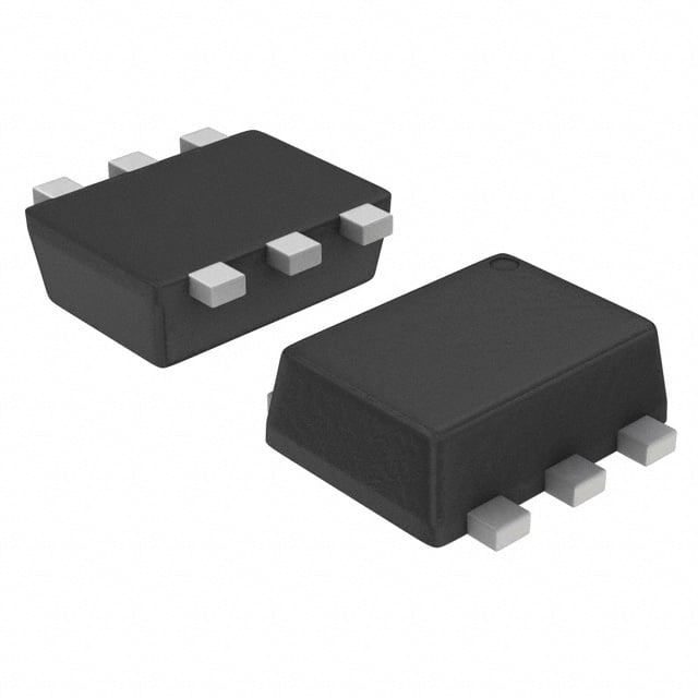
| 描述 | TVS DIODE 12VWM 25VC SOT563TVS二极管阵列 MI ZNR QUAD ARRY |
| 产品分类 | |
| 品牌 | ON Semiconductor |
| 产品手册 | |
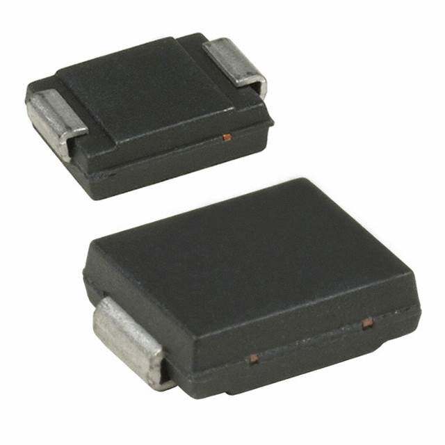
| 产品图片 |
|
| rohs | 符合RoHS无铅 / 符合限制有害物质指令(RoHS)规范要求 |
| 产品系列 | 二极管与整流器,TVS二极管,TVS二极管阵列,ON Semiconductor NUP4102XV6T1G- |
| 数据手册 | |
| 产品型号 | NUP4102XV6T1G |
| PCN设计/规格 | |
| 不同频率时的电容 | 13pF @ 1MHz |
| 产品种类 | TVS二极管阵列 |
| 供应商器件封装 | SOT-563 |
| 其它名称 | NUP4102XV6T1GOSCT |
| 击穿电压 | 17.8 V |
| 功率-峰值脉冲 | 75W |
| 包装 | 剪切带 (CT) |
| 单向通道 | - |
| 双向通道 | 4 |
| 商标 | ON Semiconductor |
| 安装类型 | 表面贴装 |
| 安装风格 | SMD/SMT |
| 封装 | Reel |
| 封装/外壳 | SOT-563,SOT-666 |
| 封装/箱体 | SOT-563 |
| 尺寸 | 1.2 mm W x 1.6 mm L |
| 峰值浪涌电流 | 3 A |
| 峰值脉冲功率耗散 | 100 W |
| 工作温度 | -40°C ~ 125°C (TJ) |
| 工作电压 | 12 V |
| 工厂包装数量 | 4000 |
| 应用 | 通用 |
| 最大工作温度 | + 125 C |
| 最小工作温度 | - 40 C |
| 极性 | Bidirectional |
| 标准包装 | 1 |
| 电压-击穿(最小值) | 13.6V |
| 电压-反向关态(典型值) | 12V (最小值) |
| 电压-箝位(最大值)@Ipp | 25V |
| 电容 | 15 pF |
| 电流-峰值脉冲(10/1000µs) | 3A (8/20µs) |
| 电源线路保护 | 无 |
| 端接类型 | SMD/SMT |
| 类型 | 齐纳 |
| 系列 | NUP4102XV6 |
| 通道 | 4 Channels |
| 钳位电压 | 25 V |


- 商务部:美国ITC正式对集成电路等产品启动337调查
- 曝三星4nm工艺存在良率问题 高通将骁龙8 Gen1或转产台积电
- 太阳诱电将投资9.5亿元在常州建新厂生产MLCC 预计2023年完工
- 英特尔发布欧洲新工厂建设计划 深化IDM 2.0 战略
- 台积电先进制程称霸业界 有大客户加持明年业绩稳了
- 达到5530亿美元!SIA预计今年全球半导体销售额将创下新高
- 英特尔拟将自动驾驶子公司Mobileye上市 估值或超500亿美元
- 三星加码芯片和SET,合并消费电子和移动部门,撤换高东真等 CEO
- 三星电子宣布重大人事变动 还合并消费电子和移动部门
- 海关总署:前11个月进口集成电路产品价值2.52万亿元 增长14.8%


PDF Datasheet 数据手册内容提取
NUP4102XV6 6−Pin Bi−Directional Quad TVS Array This 6−Pin bi−directional transient suppressor array is designed for applications requiring transient overvoltage protection capability. It is intended for use in transient voltage and ESD sensitive equipment such as computers, printers, cell phones, medical equipment, and other http://onsemi.com applications. Its integrated design provides bi−directional protection for four separate lines using a single SOT−563 package. This device is 6 ideal for situations where board space is a premium. Features • 4 Bi−directional Protection for Four Lines in a 2, 5 Single SOT−563 Package 3 • Peak Power Dissipation − 75 W (8x20 (cid:2)sec Waveform) • Low Leakage Current (100 nA @ 12 V) 1 • Low Capacitance (< 15 pF) • Provides ESD Protection for JEDEC Standards JESD22 − Machine Model = Class C − Human Body Model = Class 3B • Provides ESD Protection for IEC 61000−4−2, 15 kV (Air), SOT−563 8 kV (Contact) CASE 463A Mechanical Characteristics PLASTIC • Void Free, Transfer−Molded, Thermosetting Plastic Case • Corrosion Resistant Finish, Easily Solderable MARKING DIAGRAM • Package Designed for Optimal Automated Board Assembly • 6 5 4 Small Package Size for High Density Applications Applications RP M(cid:2) • (cid:2) GSM Handsets and Accessories • Other Telephone Sets 1 2 3 • Computers / Printers / Set−Top Boxes RP = Device Marking M = One Digit Date Code MAXIMUM RATINGS (TJ=25°C, unless otherwise specified) (cid:2) = Pb−Free Package (Note: Microdot may be in either location) Rating Symbol Value Unit Peak Power Dissipation PPK 75 W 8x20 (cid:2)sec Double Exponential Waveform, (Note 1) ORDERING INFORMATION Operating Junction Temperature Range TJ −40 to °C Device Package Shipping† 125 Storage Temperature Range TSTG −55 to °C NUP4102XV6T1G SOT−563 4000/Tape & Reel 150 (Pb−Free) Lead Solder Temperature – Maximum (10 sec) TL 260 °C †For information on tape and reel specifications, including part orientation and tape sizes, please Human Body Model ( HBM) ESD 16 kV refer to our Tape and Reel Packaging Specification Machine Model (MM) 0.4 Brochure, BRD8011/D. IEC 61000−4−2 Air (ESD) 30 IEC 61000−4−2 Contact (ESD) 30 Maximum ratings are those values beyond which device damage can occur. Maximum ratings applied to the device are individual stress limit values (not normal operating conditions) and are not valid simultaneously. If these limits are exceeded, device functional operation is not implied, damage may occur and reliability may be affected. 1. Non−repetitive current pulse per Figure 3. © Semiconductor Components Industries, LLC, 2006 1 Publication Order Number: January, 2006 − Rev. 1 NUP4102XV6/D
NUP4102XV6 ELECTRICAL CHARACTERISTICS (TJ=25°C, unless otherwise specified) Parameter Conditions Symbol Min Typ Max Unit Reverse Working Voltage (Note 2) VRWM 12 V Breakdown Voltage IT = 1 mA, (Note 3) VBR 13.6 17.8 V Reverse Leakage Current VRWM = 12 V IR 10 100 nA Clamping Voltage IPP = 3 A, (8x20 (cid:2)sec VC 25 V Waveform) Maximum Peak Pulse Current 8x20 (cid:2)sec waveform IPP 3.0 A Capacitance VR = 0 V, f=1 MHz Cj 13 15 pF (Line to GND) 2. TVS devices are normally selected according to the working peak reverse voltage (VRWM), which should be equal or greater than the DC or continuous peak operating voltage level. 3. VBR is measured at pulse test current IT; Pulse Width 1 ms. TYPICAL PERFORMANCE CURVES (TJ = 25°C unless otherwise specified) 110 110 100 WAVEFORM 100 PARAMETERS P 90 P 90 tr = 8 (cid:2)s R I PP 80 td = 20 (cid:2)s R O 80 OF I 70 c−t WE 70 T 60 O 60 N P E 50 td = IPP/2 D 50 C E R 40 T 40 E A P 30 F R 30 O 20 20 % 10 10 0 0 0 5 10 15 20 25 30 0 25 50 75 100 125 150 t, TIME ((cid:2)s) TA, AMBIENT TEMPERATURE (°C) Figure 1. Pulse Waveform Figure 2. Power Derating Curve 24 14 GE (V) 22 tPT A= =1 02 5(cid:2)°sCec E (pF) 12 A C LT N 10 O 20 A G V ACIT 8 PIN 18 AP M C 6 A N L 16 O , CP CTI 4 M N LA 14 U 2 C J V 12 0 0.1 1 10 0 1 2 3 4 5 6 7 8 9 10 11 12 13 14 IPP, SURGE CURRENT (A) VBR, REVERSE VOLTAGE (V) Figure 3. Clamping Voltage vs. Peak Pulse Figure 4. Junction Capacitance vs. Reverse Current (10 (cid:2)sec Square Wave Pulse) Voltage http://onsemi.com 2
NUP4102XV6 PACKAGE DIMENSIONS SOT−563, 6−LEAD CASE 463A−01 ISSUE O NOTES: 1. DIMENSIONING AND TOLERANCING PER ANSI Y14.5M, 1982. 2. CONTROLLING DIMENSION: MILLIMETERS A 3. MAXIMUM LEAD THICKNESS INCLUDES LEAD C −X− FINISH THICKNESS. MINIMUM LEAD THICKNESS K IS THE MINIMUM THICKNESS OF BASE MATERIAL. 6 5 4 MILLIMETERS INCHES B DIM MIN MAX MIN MAX −Y− S A 1.50 1.70 0.059 0.067 1 2 3 B 1.10 1.30 0.043 0.051 C 0.50 0.60 0.020 0.024 D 0.17 0.27 0.007 0.011 D 65 PL J G 0.50 BSC 0.020 BSC G 0.08 (0.003)M X Y KJ 00..0180 00..1380 00..000034 00..000172 S 1.50 1.70 0.059 0.067 ON Semiconductor and are registered trademarks of Semiconductor Components Industries, LLC (SCILLC). SCILLC reserves the right to make changes without further notice to any products herein. SCILLC makes no warranty, representation or guarantee regarding the suitability of its products for any particular purpose, nor does SCILLC assume any liability arising out of the application or use of any product or circuit, and specifically disclaims any and all liability, including without limitation special, consequential or incidental damages. “Typical” parameters which may be provided in SCILLC data sheets and/or specifications can and do vary in different applications and actual performance may vary over time. All operating parameters, including “Typicals” must be validated for each customer application by customer’s technical experts. SCILLC does not convey any license under its patent rights nor the rights of others. SCILLC products are not designed, intended, or authorized for use as components in systems intended for surgical implant into the body, or other applications intended to support or sustain life, or for any other application in which the failure of the SCILLC product could create a situation where personal injury or death may occur. Should Buyer purchase or use SCILLC products for any such unintended or unauthorized application, Buyer shall indemnify and hold SCILLC and its officers, employees, subsidiaries, affiliates, and distributors harmless against all claims, costs, damages, and expenses, and reasonable attorney fees arising out of, directly or indirectly, any claim of personal injury or death associated with such unintended or unauthorized use, even if such claim alleges that SCILLC was negligent regarding the design or manufacture of the part. SCILLC is an Equal Opportunity/Affirmative Action Employer. This literature is subject to all applicable copyright laws and is not for resale in any manner. PUBLICATION ORDERING INFORMATION LITERATURE FULFILLMENT: N. American Technical Support: 800−282−9855 Toll Free ON Semiconductor Website: http://onsemi.com Literature Distribution Center for ON Semiconductor USA/Canada P.O. Box 61312, Phoenix, Arizona 85082−1312 USA Order Literature: http://www.onsemi.com/litorder Phone: 480−829−7710 or 800−344−3860 Toll Free USA/Canada Japan: ON Semiconductor, Japan Customer Focus Center Fax: 480−829−7709 or 800−344−3867 Toll Free USA/Canada 2−9−1 Kamimeguro, Meguro−ku, Tokyo, Japan 153−0051 For additional information, please contact your Email: orderlit@onsemi.com Phone: 81−3−5773−3850 local Sales Representative. http://onsemi.com NUP4102XV6/D 3
Mouser Electronics Authorized Distributor Click to View Pricing, Inventory, Delivery & Lifecycle Information: O N Semiconductor: NUP4102XV6T1G