ICGOO在线商城 > 分立半导体产品 > 晶体管 - FET,MOSFET - 单 > NTR5198NLT1G
 Datasheet下载
- 型号: NTR5198NLT1G
- 制造商: ON Semiconductor
- 库位|库存: xxxx|xxxx
- 要求:
| 数量阶梯 | 香港交货 | 国内含税 |
| +xxxx | $xxxx | ¥xxxx |
查看当月历史价格
查看今年历史价格
NTR5198NLT1G产品简介:
ICGOO电子元器件商城为您提供NTR5198NLT1G由ON Semiconductor设计生产,在icgoo商城现货销售,并且可以通过原厂、代理商等渠道进行代购。 NTR5198NLT1G价格参考。ON SemiconductorNTR5198NLT1G封装/规格:晶体管 - FET,MOSFET - 单, 表面贴装 N 沟道 60V 1.7A(Ta) 900mW(Ta) SOT-23-3(TO-236)。您可以下载NTR5198NLT1G参考资料、Datasheet数据手册功能说明书,资料中有NTR5198NLT1G 详细功能的应用电路图电压和使用方法及教程。
NTR5198NLT1G 是由 ON Semiconductor(现为安森美半导体)生产的单通道 N 沟道增强型 MOSFET。该型号的应用场景广泛,适用于多种电力电子设备和电路设计中。

 1. 电源管理
NTR5198NLT1G 常用于电源管理电路中,如开关电源(SMPS)、DC-DC 转换器、线性稳压器等。其低导通电阻(Rds(on))特性有助于减少功率损耗,提高效率。在这些应用中,MOSFET 作为开关元件,能够快速响应负载变化,确保输出电压的稳定性。

 2. 电机驱动
在电机驱动应用中,NTR5198NLT1G 可以用于控制电机的启停、转向和速度调节。通过 PWM(脉宽调制)信号控制 MOSFET 的导通与关断,可以实现对电机电流的精确控制。其低导通电阻和快速开关特性使得它在电机驱动电路中表现出色,特别适合小型直流电机或步进电机的驱动。

 3. 电池管理系统
NTR5198NLT1G 还可用于电池管理系统(BMS)中,作为电池充放电路径的开关。它可以有效地防止电池过充、过放以及短路等问题。MOSFET 的低导通电阻有助于减少电池充放电过程中的能量损耗,延长电池寿命。

 4. 负载开关
在消费电子设备中,NTR5198NLT1G 可以用作负载开关,控制外围设备的供电。例如,在智能手机、平板电脑等设备中,MOSFET 可以根据需要开启或关闭某些模块的电源,从而节省电量并延长续航时间。

 5. 信号切换
在通信和数据传输领域,NTR5198NLT1G 可用于信号切换电路中。它可以作为模拟开关,选择不同的信号路径,或者在多路复用器中使用。其低电容和快速开关特性使得它在高频信号切换应用中表现出色。

 6. 保护电路
NTR5198NLT1G 还可以用于各种保护电路中,如过流保护、短路保护等。通过检测电流大小,当超过设定阈值时,MOSFET 可以迅速切断电路,防止损坏其他元器件。

总之,NTR5198NLT1G 凭借其优异的电气性能和可靠性,适用于多种应用场景,特别是在需要高效功率转换和精确电流控制的场合。
| 参数 | 数值 |
| 产品目录 | |
| 描述 | MOSFET N-CH 60V 1.7A SOT23MOSFET Pwr MOSFET 60V 2.2A 155mOhm SGL N-CH |
| 产品分类 | FET - 单分离式半导体 |
| FET功能 | 逻辑电平门 |
| FET类型 | MOSFET N 通道,金属氧化物 |
| Id-ContinuousDrainCurrent | 2.2 A |
| Id-连续漏极电流 | 2.2 A |
| 品牌 | ON Semiconductor |
| 产品手册 | |
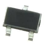
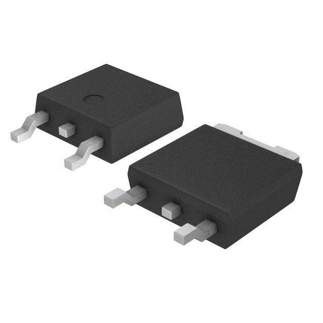
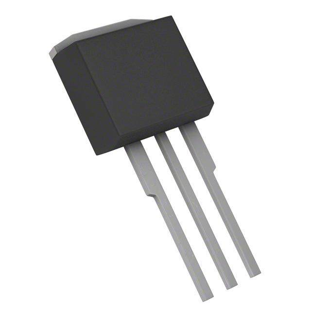
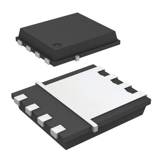
| 产品图片 |
|
| rohs | 符合RoHS无铅 / 符合限制有害物质指令(RoHS)规范要求 |
| 产品系列 | 晶体管,MOSFET,ON Semiconductor NTR5198NLT1G- |
| 数据手册 | |
| 产品型号 | NTR5198NLT1G |
| Pd-PowerDissipation | 1.5 W |
| Pd-功率耗散 | 1.5 W |
| Qg-GateCharge | 5.1 nC |
| Qg-栅极电荷 | 5.1 nC |
| RdsOn-Drain-SourceResistance | 142 mOhms |
| RdsOn-漏源导通电阻 | 142 mOhms |
| Vds-Drain-SourceBreakdownVoltage | 60 V |
| Vds-漏源极击穿电压 | 60 V |
| Vgs-Gate-SourceBreakdownVoltage | +/- 20 V |
| Vgs-栅源极击穿电压 | 20 V |
| Vgsth-Gate-SourceThresholdVoltage | 2.5 V |
| Vgsth-栅源极阈值电压 | 2.5 V |
| 上升时间 | 7 ns |
| 下降时间 | 2 ns |
| 不同Id时的Vgs(th)(最大值) | 2.5V @ 250µA |
| 不同Vds时的输入电容(Ciss) | 182pF @ 25V |
| 不同Vgs时的栅极电荷(Qg) | 2.8nC @ 4.5V |
| 不同 Id、Vgs时的 RdsOn(最大值) | 155 毫欧 @ 1A, 10V |
| 产品种类 | MOSFET |
| 供应商器件封装 | SOT-23-3(TO-236) |
| 其它名称 | NTR5198NLT1GOSDKR |
| 典型关闭延迟时间 | 13 ns |
| 功率-最大值 | 900mW |
| 包装 | Digi-Reel® |
| 商标 | ON Semiconductor |
| 安装类型 | 表面贴装 |
| 安装风格 | SMD/SMT |
| 导通电阻 | 142 mOhms |
| 封装 | Reel |
| 封装/外壳 | TO-236-3,SC-59,SOT-23-3 |
| 封装/箱体 | SOT-23-3 |
| 工厂包装数量 | 3000 |
| 晶体管极性 | N-Channel |
| 标准包装 | 1 |
| 正向跨导-最小值 | 3 S |
| 汲极/源极击穿电压 | 60 V |
| 漏极连续电流 | 2.2 A |
| 漏源极电压(Vdss) | 60V |
| 电流-连续漏极(Id)(25°C时) | 1.7A (Ta) |
| 系列 | NTR5198NL |
| 配置 | Single |


PDF Datasheet 数据手册内容提取
NTR5198NL Power MOSFET (cid:2) 60 V, 155 m , Single N−Channel Logic Level, SOT−23 Features • Small Footprint Industry Standard Surface Mount SOT−23 Package www.onsemi.com • Low R for Low Conduction Losses and Improved Efficiency DS(on) • These Devices are Pb−Free, Halogen Free/BFR Free and are RoHS V(BR)DSS RDS(on) TYP ID MAX Compliant 155 m(cid:5) @ 10 V 60 V 2.2 A MAXIMUM RATINGS (TJ = 25°C unless otherwise noted) 205 m(cid:5) @ 4.5 V Parameter Symbol Value Unit Drain−to−Source Voltage VDSS 60 V N−Channel Gate−to−Source Voltage VGS ±20 V D Continuous Drain Steady TA = 25°C ID 2.2 A C(Nuortreesn t1 R, 2(cid:2),J −3m, abnd 4) State TA = 100°C 1.6 Power Dissipation TA = 25°C PD 1.5 W G R(N(cid:2)oJt−ems b1 and 3) TA = 100°C 0.6 Continuous Drain Steady TA = 25°C ID 1.7 A S C(Nuortree n1t, R2(cid:3), J3A, and 4) State TA = 100°C 1.2 Power Dissipation R(cid:3)JA TA = 25°C PD 0.9 W 3 MARKING DIAGRAM/ (Notes 1 and 3) PIN ASSIGNMENT TA = 100°C 0.4 Pulsed Drain Current TA = 25°C, IDM 27 A 1 Drain tp =10 (cid:4)s 2 3 Operating Junction and Storage Temperature TJ, −55 to °C SOT−23 AA6(cid:2) M(cid:2) Tstg 150 CASE 318 1 2 Source Current (Body Diode) IS 1.9 A STYLE 21 Gate Source Lead Temperature for Soldering Purposes TL 260 °C (1/8” from case for 10 s) AA6 = Device Code Stresses exceeding those listed in the Maximum Ratings table may damage the M = Date Code* device. If any of these limits are exceeded, device functionality should not be (cid:2) = Pb−Free Package assumed, damage may occur and reliability may be affected. (Note: Microdot may be in either location) 1. The entire application environment impacts the thermal resistance values shown, they are not constants and are only valid for the particular conditions *Date Code orientation may vary depending noted. upon manufacturing location. 2. Psi ((cid:2)) is used as required per JESD51−12 for packages in which substantially less than 100% of the heat flows to single case surface. 3. Surface−mounted on FR4 board using a 650 mm2, 2 oz. Cu pad. ORDERING INFORMATION 4. Maximum current for pulses as long as 1 second is higher but is dependent on pulse duration and duty cycle. Device Package Shipping† NTR5198NLT1G SOT−23 3000 / (Pb−Free) Tape & Reel NTR5198NLT3G SOT−23 10000 / (Pb−Free) Tape & Reel †For information on tape and reel specifications, including part orientation and tape sizes, please refer to our Tape and Reel Packaging Specification Brochure, BRD8011/D. © Semiconductor Components Industries, LLC, 2013 1 Publication Order Number: October, 2016 − Rev. 2 NTR5198NL/D
NTR5198NL THERMAL RESISTANCE RATINGS Parameter Symbol Max Unit Junction−to−Lead #3 − Drain (Notes 2 and 3) R(cid:2)J−mb 86 °C/W Junction−to−Ambient − Steady State (Note 3) R(cid:3)JA 139 °C/W ELECTRICAL CHARACTERISTICS (TJ = 25°C unless otherwise noted) Parameter Symbol Test Conditions Min Typ Max Unit OFF CHARACTERISTICS Drain−to−Source Breakdown Voltage V(BR)DSS VGS = 0 V, ID = 250 (cid:4)A 60 V Drain−to−Source Breakdown Voltage V(BR)DSS/TJ Reference to 25°C, ID = 250 (cid:4)A 70 mV/°C Temperature Coefficient Zero Gate Voltage Drain Current IDSS VGS = 0 V, TJ = 25°C 1.0 (cid:4)A VDS = 60 V TJ = 125°C 10 Gate−to−Source Leakage Current IGSS VDS = 0 V, VGS = (cid:2)20 V (cid:2)100 nA ON CHARACTERISTICS (Note 5) Gate Threshold Voltage VGS(TH) VGS = VDS, ID = 250 (cid:4)A 1.5 2.5 V Threshold Temperature Coefficient VGS(TH)/TJ Reference to 25°C, ID = 250 (cid:4)A −6.5 mV/°C Drain−to−Source On−Resistance RDS(on) VGS = 10 V, ID = 1 A 107 155 m(cid:5) VGS = 4.5 V, ID = 1 A 142 205 Forward Transconductance gFS VDS = 5.0 V, ID = 1 A 3 S CHARGES, CAPACITANCES & GATE RESISTANCE Input Capacitance Ciss 182 pF Output Capacitance Coss VGS = V0D VS, =f =2 51 .V0 MHz, 25 Reverse Transfer Capacitance Crss 16 Total Gate Charge QG(TOT) VDS = 48 V, VGS = 4.5 V 2.8 nC ID = 1 A VGS = 10 V 5.1 Threshold Gate Charge QG(TH) 0.3 Gate−to−Source Charge QGS VDS = 48 V, ID = 1 A 0.8 Gate−to−Drain Charge QGD VGS = 10 V 1.5 Plateau Voltage VGP 3.1 V Gate Resistance RG 8 (cid:5) SWITCHING CHARACTERISTICS (Note 6) Turn−On Delay Time td(on) 5 ns Rise Time tr VDS = 30 V, VGS = 10 V, 7 Turn−Off Delay Time td(off) ID = 1 A, RG = 10(cid:6)(cid:5) 13 Fall Time tf 2 DRAIN−SOURCE DIODE CHARACTERISTICS Forward Diode Voltage VSD VGS = 0 V, TJ = 25°C 0.8 1.2 V IS = 1 A TJ = 125°C 0.6 Reverse Recovery Time trr 12 ns Charge Time ta IS = 1 Adc, VGS = 0 Vdc, 9 Discharge Time tb dIS/dt = 100 A/(cid:4)s 3 Reverse Recovery Stored Charge QRR 6 nC Product parametric performance is indicated in the Electrical Characteristics for the listed test conditions, unless otherwise noted. Product performance may not be indicated by the Electrical Characteristics if operated under different conditions. 5. Pulse Test: Pulse Width (cid:3) 300 (cid:4)s, Duty Cycle (cid:3) 2%. 6. Switching characteristics are independent of operating junction temperatures. www.onsemi.com 2
NTR5198NL TYPICAL CHARACTERISTICS 15 15 1134 VGS = 10 V VGS = 6.0 V 1134 VDS = 5 V A) 12 VGS = 5.0 V A) 12 NT ( 1101 VGS = 4.5 V NT ( 1101 E E R 9 R 9 UR 8 UR 8 C 7 VGS = 3.0 V VGS = 4.0 V C 7 RAIN 56 VGS = 3.8 V RAIN 56 TJ = 25°C I, DD 234 VVVGGGSSS === 333...426 VVV I, DD 324 TJ = 150°C 1 1 TJ = −55°C 0 0 0 1 2 3 4 5 1 2 3 4 5 VDS, DRAIN−TO−SOURCE VOLTAGE (V) VGS, GATE−TO−SOURCE VOLTAGE (V) Figure 1. On−Region Characteristics Figure 2. Transfer Characteristics (cid:5)) (cid:5)) E ( 0.50 E ( 0.50 C C SISTAN 00..4405 ITDJ == 12 5A°C SISTAN 00..4450 TJ = 25°C VGS = 4.5 V E E R 0.35 R 0.35 E E RC 0.30 RC 0.30 U U O 0.25 O 0.25 S S − − TO 0.20 TO 0.20 VGS = 10 V − − N 0.15 N 0.15 AI AI R R D 0.10 D 0.10 , n)0.05 , n) 0.05 o o S( 3 4 5 6 7 8 9 10 S( 0 1 2 3 4 5 6 7 8 9 10 11 12 13 1415 D D R R VGS, GATE VOLTAGE (V) ID, DRAIN CURRENT (A) Figure 3. On−Resistance vs. Gate−to−Source Figure 4. On−Resistance vs. Drain Current and d) Voltage Gate Voltage E (Normalize 2111....0789 VIDG =S 1= A10 V N VOLTAGE 111...111025050 ID = 250 (cid:4)A C W N 1.6 O 1.075 TA 1.5 D S K 1.050 SI 1.4 EA RE 1.3 BR 1.025 RCE 11..12 ZED 1.000 OU 1.0 ALI 0.975 AIN−TO−S 0000....6789 , NORMSS000...999025050 R −50 −25 0 25 50 75 100 125 150 D −50 −25 0 25 50 75 100 125 150 D V , n) TJ, JUNCTION TEMPERATURE (°C) B TJ, JUNCTION TEMPERATURE (°C) o DS( Figure 5. On−Resistance Variation with Figure 6. Breakdown Voltage Variation with R Temperature Temperature www.onsemi.com 3
NTR5198NL TYPICAL CHARACTERISTICS E 1.20 10,000 G TA 1.15 ID = 250 (cid:4)A OL 1.10 TJ = 150°C V D 1.05 A) 1000 HOL 1.00 E (n TJ = 125°C S 0.95 G E A R 0.90 K 100 H A T 0.85 E ED 0.80 , LS TJ = 85°C Z S ALI 0.75 ID 10 M 0.70 R O 0.65 N , S(th)0.60−50 −25 0 25 50 75 100 125 150 10 5 10 15 20 25 30 35 40 45 50 55 60 VG TJ, JUNCTION TEMPERATURE (°C) VDS, DRAIN−TO−SOURCE VOLTAGE (V) Figure 7. Threshold Voltage Variation with Figure 8. Drain−to−Source Leakage Current Temperature vs. Voltage 227550 Tf =J =1 2M5H°Cz GE (V)1121 QT 5650GE (V) pF) 220205 CISS VGS = 0 V OLTA109 4550OLTA C, CAPACITANCE ( 1111570257050505 COSS GATE−TO−SOURCE V 3572468 QGS VDSQGD VGS VITDJD =S= 1=2 5A4°8C V 12312345550000DRAIN−TO−SOURCE V 250 CRSS V, GS 01 05 V, DS 0 5 10 15 20 25 30 35 40 45 50 55 60 0 0.5 1.0 1.5 2.0 2.5 3.0 3.5 4.0 4.5 5.0 5.5 VDS, DRAIN−TO−SOURCE VOLTAGE (V) QG, TOTAL GATE CHARGE (nC) Figure 9. Capacitance Variation Figure 10. Gate−to−Source and Drain−to−Source Voltage vs. Total Charge 100 10 VDD = 30 V TJ = 150°C td(off) VIDG =S 1= A10 V T (A) TJ = 125°C s) 10 tr REN TJ = 100°C n R t, TIME ( 1 td(tofn) URCE CU 1 TJ = 85°C O S , S I TJ = 25°C TJ = −55°C 0.1 0.1 1 10 100 0.4 0.5 0.6 0.7 0.8 0.9 1.0 1.1 RG, GATE RESISTANCE ((cid:5)) VSD, SOURCE−TO−DRAIN VOLTAGE (V) Figure 11. Resistive Switching Time Variation Figure 12. Diode Forward Voltage vs. Current vs. Gate Resistance www.onsemi.com 4
NTR5198NL TYPICAL CHARACTERISTICS 100 VGS ≤ 10 V Single Pulse A) TC = 25°C 10 (cid:4)S T ( 10 N E RR 100 (cid:4)S CU 1 1 mS N AI R 10 mS D I, D 0.1 RDS(on) Limit Thermal Limit Package Limit dc 0.01 0.1 1 10 100 VDS, DRAIN−TO−SOURCE VOLTAGE (V) W) C/ Figure 13. Maximum Rated Forward Biased °E ( Safe Operating Area S N O1000 P S E R L A M R 100 50% Duty Cycle E H T T 20% N SIE 10% R(cid:3)JA Steady State = 139°C/W N 10 5% A R E T 2% CTIV 1% Single Pulse E 1 F 0.000001 0.00001 0.0001 0.001 0.01 0.1 1 10 100 1000 F E R(t), Figure 14. Thermal Imtp, eTdIMaEn c(see c(J)unction−to−Ambient) www.onsemi.com 5
NTR5198NL PACKAGE DIMENSIONS SOT−23 (TO−236) CASE 318−08 ISSUE AR D NOTES: 1.DIMENSIONING AND TOLERANCING PER ASME Y14.5M, 1994. 2.CONTROLLING DIMENSION: MILLIMETERS. 3.MAXIMUM LEAD THICKNESS INCLUDES LEAD FINISH. 0.25 MINIMUM LEAD THICKNESS IS THE MINIMUM THICKNESS OF 3 THE BASE MATERIAL. E HE T 4.DPIRMOETNRSUIOSNIOSN DS ,A ONRD GEA DTOE NBOURT RINSC.LUDE MOLD FLASH, 1 2 MILLIMETERS INCHES DIM MIN NOM MAX MIN NOM MAX L A 0.89 1.00 1.11 0.035 0.039 0.044 3Xb L1 A1 0.01 0.06 0.10 0.000 0.002 0.004 b 0.37 0.44 0.50 0.015 0.017 0.020 e VIEW C c 0.08 0.14 0.20 0.003 0.006 0.008 TOP VIEW D 2.80 2.90 3.04 0.110 0.114 0.120 E 1.20 1.30 1.40 0.047 0.051 0.055 e 1.78 1.90 2.04 0.070 0.075 0.080 L 0.30 0.43 0.55 0.012 0.017 0.022 A L1 0.35 0.54 0.69 0.014 0.021 0.027 HE 2.10 2.40 2.64 0.083 0.094 0.104 T 0(cid:3) −−− 10(cid:3) 0(cid:3) −−− 10(cid:3) A1 c SIDE VIEW SEE VIEW C STYLE 21: END VIEW PIN 1. GATE 2. SOURCE 3. DRAIN RECOMMENDED SOLDERING FOOTPRINT* 3X 2.90 0.90 3X0.80 0.95 PITCH DIMENSIONS: MILLIMETERS *For additional information on our Pb−Free strategy and soldering details, please download the ON Semiconductor Soldering and Mounting Techniques Reference Manual, SOLDERRM/D. ON Semiconductor and are trademarks of Semiconductor Components Industries, LLC dba ON Semiconductor or its subsidiaries in the United States and/or other countries. ON Semiconductor owns the rights to a number of patents, trademarks, copyrights, trade secrets, and other intellectual property. A listing of ON Semiconductor’s product/patent coverage may be accessed at www.onsemi.com/site/pdf/Patent−Marking.pdf. ON Semiconductor reserves the right to make changes without further notice to any products herein. ON Semiconductor makes no warranty, representation or guarantee regarding the suitability of its products for any particular purpose, nor does ON Semiconductor assume any liability arising out of the application or use of any product or circuit, and specifically disclaims any and all liability, including without limitation special, consequential or incidental damages. Buyer is responsible for its products and applications using ON Semiconductor products, including compliance with all laws, regulations and safety requirements or standards, regardless of any support or applications information provided by ON Semiconductor. “Typical” parameters which may be provided in ON Semiconductor data sheets and/or specifications can and do vary in different applications and actual performance may vary over time. All operating parameters, including “Typicals” must be validated for each customer application by customer’s technical experts. ON Semiconductor does not convey any license under its patent rights nor the rights of others. ON Semiconductor products are not designed, intended, or authorized for use as a critical component in life support systems or any FDA Class 3 medical devices or medical devices with a same or similar classification in a foreign jurisdiction or any devices intended for implantation in the human body. Should Buyer purchase or use ON Semiconductor products for any such unintended or unauthorized application, Buyer shall indemnify and hold ON Semiconductor and its officers, employees, subsidiaries, affiliates, and distributors harmless against all claims, costs, damages, and expenses, and reasonable attorney fees arising out of, directly or indirectly, any claim of personal injury or death associated with such unintended or unauthorized use, even if such claim alleges that ON Semiconductor was negligent regarding the design or manufacture of the part. ON Semiconductor is an Equal Opportunity/Affirmative Action Employer. This literature is subject to all applicable copyright laws and is not for resale in any manner. PUBLICATION ORDERING INFORMATION LITERATURE FULFILLMENT: N. American Technical Support: 800−282−9855 Toll Free ON Semiconductor Website: www.onsemi.com Literature Distribution Center for ON Semiconductor USA/Canada 19521 E. 32nd Pkwy, Aurora, Colorado 80011 USA Europe, Middle East and Africa Technical Support: Order Literature: http://www.onsemi.com/orderlit Phone: 303−675−2175 or 800−344−3860 Toll Free USA/Canada Phone: 421 33 790 2910 Fax: 303−675−2176 or 800−344−3867 Toll Free USA/Canada Japan Customer Focus Center For additional information, please contact your local Email: orderlit@onsemi.com Phone: 81−3−5817−1050 Sales Representative ◊ www.onsemi.com NTR5198NL/D 6
Mouser Electronics Authorized Distributor Click to View Pricing, Inventory, Delivery & Lifecycle Information: O N Semiconductor: NTR5198NLT1G NTR5198NLT3G