ICGOO在线商城 > 分立半导体产品 > 晶体管 - FET,MOSFET - 单 > NTP6412ANG

 Datasheet下载
- 型号: NTP6412ANG
- 制造商: ON Semiconductor
- 库位|库存: xxxx|xxxx
- 要求:
| 数量阶梯 | 香港交货 | 国内含税 |
| +xxxx | $xxxx | ¥xxxx |
查看当月历史价格
查看今年历史价格
NTP6412ANG产品简介:
ICGOO电子元器件商城为您提供NTP6412ANG由ON Semiconductor设计生产,在icgoo商城现货销售,并且可以通过原厂、代理商等渠道进行代购。 NTP6412ANG价格参考。ON SemiconductorNTP6412ANG封装/规格:晶体管 - FET,MOSFET - 单, 通孔 N 沟道 100V 58A(Tc) 167W(Tc) TO-220AB。您可以下载NTP6412ANG参考资料、Datasheet数据手册功能说明书,资料中有NTP6412ANG 详细功能的应用电路图电压和使用方法及教程。
安森美半导体(ON Semiconductor)的NTP6412ANG是一款N沟道增强型MOSFET,广泛应用于需要高效功率开关的场景。其主要应用场景包括:

1. 电源管理:适用于DC-DC转换器、同步整流器等电源模块,提高能效并减小体积。
2. 电机驱动:用于电动工具、风扇、泵等电机控制电路,提供高开关速度和低导通电阻。
3. 负载开关:作为高侧或低侧开关控制负载通断,如LED照明、加热元件等。
4. 电池供电设备:常见于笔记本电脑、移动电源、无人机等便携设备中,实现高效能与低功耗。
5. 工业自动化:用于PLC、工业电机控制和传感器供电系统,具备高可靠性和耐久性。

该器件具有低导通电阻(Rds(on))、高电流承载能力和优良的热性能,适合高频开关应用。
| 参数 | 数值 |
| 产品目录 | |
| 描述 | MOSFET N-CH 100V 58A TO-220ABMOSFET NFET TO220 100V 72A |
| 产品分类 | FET - 单分离式半导体 |
| FET功能 | 标准 |
| FET类型 | MOSFET N 通道,金属氧化物 |
| Id-ContinuousDrainCurrent | 58 A |
| Id-连续漏极电流 | 58 A |
| 品牌 | ON Semiconductor |
| 产品手册 | |
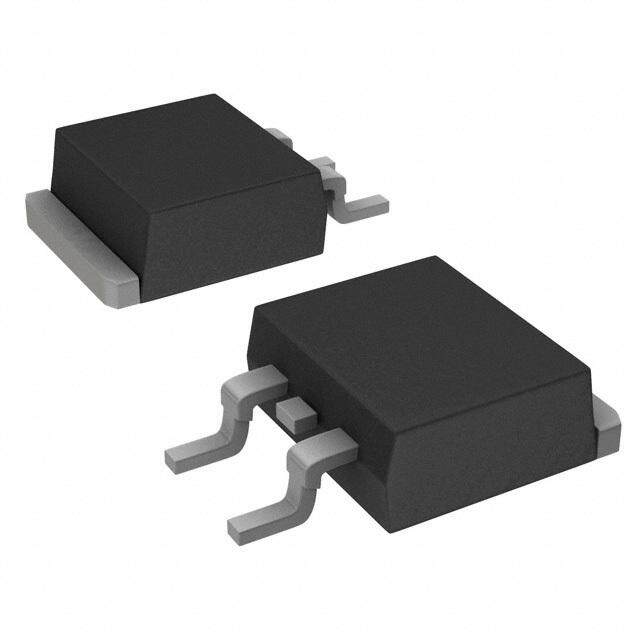
| 产品图片 |
|
| rohs | 符合RoHS无铅 / 符合限制有害物质指令(RoHS)规范要求 |
| 产品系列 | 晶体管,MOSFET,ON Semiconductor NTP6412ANG- |
| 数据手册 | |
| 产品型号 | NTP6412ANG |
| PCN设计/规格 | |
| Pd-PowerDissipation | 167 W |
| Pd-功率耗散 | 167 W |
| RdsOn-Drain-SourceResistance | 18.2 mOhms |
| RdsOn-漏源导通电阻 | 18.2 mOhms |
| Vds-Drain-SourceBreakdownVoltage | 100 V |
| Vds-漏源极击穿电压 | 100 V |
| Vgs-Gate-SourceBreakdownVoltage | +/- 20 V |
| Vgs-栅源极击穿电压 | 20 V |
| 不同Id时的Vgs(th)(最大值) | 4V @ 250µA |
| 不同Vds时的输入电容(Ciss) | 3500pF @ 25V |
| 不同Vgs时的栅极电荷(Qg) | 100nC @ 10V |
| 不同 Id、Vgs时的 RdsOn(最大值) | 18.2 毫欧 @ 58A,10V |
| 产品种类 | MOSFET |
| 供应商器件封装 | TO-220AB |
| 其它名称 | NTP6412ANG-ND |
| 功率-最大值 | 167W |
| 包装 | 管件 |
| 商标 | ON Semiconductor |
| 安装类型 | 通孔 |
| 安装风格 | SMD/SMT |
| 封装/外壳 | TO-220-3 |
| 封装/箱体 | D2PAK-2 |
| 工厂包装数量 | 50 |
| 晶体管极性 | N-Channel |
| 最大工作温度 | + 175 C |
| 最小工作温度 | - 55 C |
| 标准包装 | 50 |
| 漏源极电压(Vdss) | 100V |
| 电流-连续漏极(Id)(25°C时) | 58A (Tc) |
| 系列 | NTP6412AN |
| 配置 | Single |


PDF Datasheet 数据手册内容提取
NTB6412AN, NTP6412AN, NVB6412AN N-Channel Power MOSFET 100 V, 58 A, 18.2 m(cid:2) Features • Low R DS(on) www.onsemi.com • High Current Capability • 100% Avalanche Tested • ID MAX NVB Prefix for Automotive and Other Applications Requiring V(BR)DSS RDS(ON) MAX (Note 1) Unique Site and Control Change Requirements; AEC−Q101 100 V 18.2 m(cid:4) @ 10 V 58 A Qualified and PPAP Capable • These Devices are Pb−Free and are RoHS Compliant N−Channel D MAXIMUM RATINGS (TJ = 25°C Unless otherwise specified) Parameter Symbol Value Unit Drain−to−Source Voltage VDSS 100 V Gate−to−Source Voltage − Continuous VGS (cid:2)20 V G Continuous Drain Cur- Steady TC = 25°C ID 58 A rent R(cid:2)JC State TC = 100°C 41 S Power Dissipation Steady TC = 25°C PD 167 W 4 R(cid:2)JC State 4 Pulsed Drain Current tp = 10 (cid:3)s IDM 240 A Operating Junction and Storage Temperature TJ, Tstg −55 to °C 1 2 Range +175 3 Source Current (Body Diode) IS 58 A TO−220AB D2PAK SEinnegrlgey P (uVlDseD D= r5a0in V−tdoc−, SVoGuSrc =e 1A0v aVldacn,che EAS 300 mJ 12 CSATSYEL 2E2 15A CSATSYEL 4E1 82B IL(pk) = 44.7 A, L = 0.3 mH, RG = 25 (cid:4)) 3 LPeuarpdo Tseems,p 1e/r8a″t ufrroem fo Cr Sasoeld feorri n1g0 Seconds TL 260 °C MARKING DIAGRAM & PIN ASSIGNMENT 4 THERMAL RESISTANCE RATINGS 4 Drain Drain Parameter Symbol Max Unit Junction−to−Case (Drain) Steady State R(cid:2)JC 0.9 °C/W Junction−to−Ambient (Note 1) R(cid:2)JA 33 NTB NTP 6412ANG Stresses exceeding those listed in the Maximum Ratings table may damage the 6412ANG AYWW device. If any of these limits are exceeded, device functionality should not be AYWW assumed, damage may occur and reliability may be affected. 1. Surface mounted on FR4 board using 1 sq in pad size, 1 3 1 2 3 (Cu Area 1.127 sq in [2 oz] including traces). Gate Source Gate Drain Source 2 6412AN = Specific Device Code Drain G = Pb−Free Device A = Assembly Location Y = Year WW = Work Week ORDERING INFORMATION See detailed ordering and shipping information in the package dimensions section on page 5 of this data sheet. © Semiconductor Components Industries, LLC, 2015 1 Publication Order Number: January, 2015 − Rev. 2 NTB6412AN/D
NTB6412AN, NTP6412AN, NVB6412AN ELECTRICAL CHARACTERISTICS (TJ = 25°C Unless otherwise specified) Characteristics Symbol Test Condition Min Typ Max Unit OFF CHARACTERISTICS Drain−to−Source Breakdown Voltage V(BR)DSS VGS = 0 V, ID = 250 (cid:3)A 100 V Drain−to−Source Breakdown Voltage Temper- V(BR)DSS/TJ 103 mV/°C ature Coefficient Zero Gate Voltage Drain Current IDSS VGS = 0 V, TJ = 25°C 1.0 (cid:3)A VDS = 100 V TJ = 125°C 100 Gate−to−Source Leakage Current IGSS VDS = 0 V, VGS = (cid:2)20 V (cid:2)100 nA ON CHARACTERISTICS (Note 2) Gate Threshold Voltage VGS(th) VGS = VDS, ID = 250 (cid:3)A 2.0 4.0 V Negative Threshold Temperature Coefficient VGS(th)/TJ 9.2 mV/°C Drain−to−Source On−Resistance RDS(on) VGS = 10 V, ID = 58 A 16.8 18.2 m(cid:4) VGS = 10 V, ID = 20 A 15.6 18.2 Forward Transconductance gFS VDS = 5 V, ID = 20 A 31 S CHARGES, CAPACITANCES & GATE RESISTANCE Input Capacitance Ciss 2700 3500 pF Output Capacitance Coss VDS = f2 =5 1V ,M VHGzS = 0 V, 400 500 Reverse Transfer Capacitance Crss 150 Total Gate Charge QG(TOT) 73 100 nC Threshold Gate Charge QG(TH) 2.5 Gate−to−Source Charge QGS VGS = 1I0D V=, 5V8D AS = 80 V, 13.5 Gate−to−Drain Charge QGD 35 Plateau Voltage VGP 5.6 V Gate Resistance RG 2.2 (cid:4) SWITCHING CHARACTERISTICS, VGS = 10 V (Note 3) Turn−On Delay Time td(on) 16 ns Rise Time tr VGS = 10 V, VDD = 80 V, 140 Turn−Off Delay Time td(off) ID = 58 A, RG = 6.2(cid:5)(cid:4) 70 Fall Time tf 126 DRAIN−SOURCE DIODE CHARACTERISTICS Forward Diode Voltage VSD TJ = 25°C 0.96 1.3 V IS = 58 A TJ = 125°C 0.89 Reverse Recovery Time trr 85 ns Charge Time ta VGS = 0 V, IS = 58 A, 60 Discharge Time tb dISD/dt = 100 A/(cid:3)s 25 Reverse Recovery Charge QRR 270 nC 2. Pulse Test: Pulse Width ≤ 300 (cid:3)s, Duty Cycle ≤ 2%. 3. Switching characteristics are independent of operating junction temperatures. www.onsemi.com 2
NTB6412AN, NTP6412AN, NVB6412AN 120 120 TJ = 25°C VDS (cid:3) 10 V 7.5 V 100 6.5 V 100 A) 10 V A) T ( T ( N 80 N 80 E 6.0 V E R R R R U 60 U 60 C C N N RAI 40 5.4 V RAI 40 TJ = 125°C TJ = 25°C D D , D 5.0 V , D I 20 I 20 VGS = 4.4 V TJ = −55°C 0 0 0 1 2 3 4 5 2 3 4 5 6 7 8 VDS, DRAIN−TO−SOURCE VOLTAGE (V) VGS, GATE−TO−SOURCE VOLTAGE (V) Figure 1. On−Region Characteristics Figure 2. Transfer Characteristics (cid:4)) (cid:4)) E ( 0.04 E ( 0.06 C ID = 58 A C TAN TJ = 25°C TAN 0.05 VGS = 10 V SIS SIS TJ = 175°C E E R 0.03 R 0.04 CE CE TJ = 125°C R R U U 0.03 O O S S − − TO 0.02 TO 0.02 TJ = 25°C − − N N AI AI 0.01 TJ = −55°C R R D D , on) 0.01 , on) 0 S( 5 6 7 8 9 10 S( 10 20 30 40 50 60 D D R R VGS, GATE−TO−SOURCE VOLTAGE (V) ID, DRAIN CURRENT (A) Figure 3. On−Region versus Gate Voltage Figure 4. On−Resistance versus Drain Current and Gate Voltage 3 100000 CE ID = 58 A VGS = 0 V N VGS = 10 V A 2.5 T RESIS 2 E (nA) 10000 TJ = 150°C O−SOURCE RMALIZED)1.5 , LEAKAGSS 1000 TJ = 125°C TO D N−(N 1 I AI R D , n) 0.5 100 S(o −50 −25 0 25 50 75 100 125 150 175 10 20 30 40 50 60 70 80 90 100 D R TJ, JUNCTION TEMPERATURE (°C) VDS, DRAIN−TO−SOURCE VOLTAGE (V) Figure 5. On−Resistance Variation with Figure 6. Drain−to−Source Leakage Current Temperature versus Voltage www.onsemi.com 3
NTB6412AN, NTP6412AN, NVB6412AN 5000 TVJG =S =2 50° VC GE (V)10 QT 100GE (V) pF) 4000 OLTA 8 VDS VGS 80 OLTA C, CAPACITANCE ( 123000000000 Ciss ATE−TO−SOURCE V 246 Qgs Qgd VDS = 80 V 642000 RAIN−TO−SOURCE V 0 Crss Coss V, GGS 0 TIDJ == 2558° AC 0 V, DDS 0 10 20 30 40 50 60 70 80 90 100 0 10 20 30 40 50 60 70 VDS, DRAIN−TO−SOURCE VOLTAGE (V) Qg, TOTAL GATE CHARGE (nC) Figure 7. Capacitance Variation Figure 8. Gate−to−Source Voltage and Drain−to−Source Voltage versus Total Charge 1000 60 VDS = 80 V TJ = 25°C ID = 58 A 50 VGS = 0 V VGS = 10 V A) tf T ( s) 100 tr REN 40 ME (n td(off) CUR 30 t, TI 10 td(on) URCE 20 O S , S 10 I 1 0 1 10 100 0.5 0.6 0.7 0.8 0.9 1.0 RG, GATE RESISTANCE ((cid:4)) VSD, SOURCE−TO−DRAIN VOLTAGE (V) Figure 9. Resistive Switching Time Variation Figure 10. Diode Forward Voltage versus versus Gate Resistance Current 1000 300 ID = 44.7 A T (A) 100 10 (cid:3)s Y (mJ) N G 200 RRE 100 (cid:3)s NER AIN CU 10 11 0m mss CHE E R N 100 D dc A I, D 1 RDS(on) LIMIT VGS = 10 V VAL THERMAL LIMIT SINGLE PULSE A PACKAGE LIMIT TC = 25°C 0.1 0 1 10 100 1000 25 50 75 100 125 150 175 VDS, DRAIN−TO−SOURCE VOLTAGE (V) TJ, STARTING JUNCTION TEMPERATURE Figure 11. Maximum Rated Forward Biased Figure 12. Maximum Avalanche Energy versus Safe Operating Area Starting Junction Temperature www.onsemi.com 4
NTB6412AN, NTP6412AN, NVB6412AN 1 D = 0.5 0.2 0.1 0.1 0.05 W) C/ 0.02 ° R(t) ( 0.01 0.01 SINGLE PULSE 0.001 0.000001 0.00001 0.0001 0.001 0.01 0.1 1 10 100 1000 t, PULSE TIME (s) Figure 13. Thermal Response ORDERING INFORMATION Device Package Shipping† NTB6412ANG D2PAK 50 Units / Rail (Pb−Free) NTB6412ANT4G D2PAK 800 / Tape & Reel (Pb−Free) NTP6412ANG TO−220 50 Units / Rail (Pb−Free) NVB6412ANT4G D2PAK 800 / Tape & Reel (Pb−Free) †For information on tape and reel specifications, including part orientation and tape sizes, please refer to our Tape and Reel Packaging Specifications Brochure, BRD8011/D. www.onsemi.com 5
NTB6412AN, NTP6412AN, NVB6412AN PACKAGE DIMENSIONS D2PAK 3 CASE 418B−04 ISSUE K NOTES: C 1. DIMENSIONING AND TOLERANCING PER ANSI Y14.5M, 1982. E 2. CONTROLLING DIMENSION: INCH. V 3. 418B−01 THRU 418B−03 OBSOLETE, −B− NEW STANDARD 418B−04. W 4 INCHES MILLIMETERS DIM MIN MAX MIN MAX A 0.340 0.380 8.64 9.65 B 0.380 0.405 9.65 10.29 A C 0.160 0.190 4.06 4.83 S D 0.020 0.035 0.51 0.89 1 2 3 E 0.045 0.055 1.14 1.40 F 0.310 0.350 7.87 8.89 G 0.100 BSC 2.54 BSC −T− H 0.080 0.110 2.03 2.79 K J 0.018 0.025 0.46 0.64 SEATING W PLANE G J KL 00..009502 00..011702 21..2392 21..7893 M 0.280 0.320 7.11 8.13 H N 0.197 REF 5.00 REF D3 PL P 0.079 REF 2.00 REF R 0.039 REF 0.99 REF 0.13 (0.005) M T B M S 0.575 0.625 14.60 15.88 V 0.045 0.055 1.14 1.40 VARIABLE CONFIGURATION STYLE 2: ZONE N P PIN 1.GATE R 2.DRAIN U 3.SOURCE 4.DRAIN L L L M M M F F F VIEW W−W VIEW W−W VIEW W−W 1 2 3 SOLDERING FOOTPRINT* 10.49 8.38 16.155 2X 3.504 2X 1.016 5.080 PITCH DIMENSIONS: MILLIMETERS *For additional information on our Pb−Free strategy and soldering details, please download the ON Semiconductor Soldering and Mounting Techniques Reference Manual, SOLDERRM/D. www.onsemi.com 6
NTB6412AN, NTP6412AN, NVB6412AN PACKAGE DIMENSIONS TO−220 CASE 221A−09 ISSUE AH NOTES: 1. DIMENSIONING AND TOLERANCING PER ANSI Y14.5M, 1982. SEATING −T− PLANE 2. CONTROLLING DIMENSION: INCH. 3. DIMENSION Z DEFINES A ZONE WHERE ALL B F C BODY AND LEAD IRREGULARITIES ARE T S ALLOWED. INCHES MILLIMETERS 4 DIM MIN MAX MIN MAX A 0.570 0.620 14.48 15.75 Q A B 0.380 0.415 9.66 10.53 C 0.160 0.190 4.07 4.83 1 2 3 U D 0.025 0.038 0.64 0.96 F 0.142 0.161 3.61 4.09 H G 0.095 0.105 2.42 2.66 H 0.110 0.161 2.80 4.10 K J 0.014 0.024 0.36 0.61 Z K 0.500 0.562 12.70 14.27 L 0.045 0.060 1.15 1.52 N 0.190 0.210 4.83 5.33 L R Q 0.100 0.120 2.54 3.04 R 0.080 0.110 2.04 2.79 V J S 0.045 0.055 1.15 1.39 T 0.235 0.255 5.97 6.47 G U 0.000 0.050 0.00 1.27 D V 0.045 --- 1.15 --- Z --- 0.080 --- 2.04 N STYLE 5: PIN 1. GATE 2. DRAIN 3. SOURCE 4. DRAIN ON Semiconductor and are registered trademarks of Semiconductor Components Industries, LLC (SCILLC). SCILLC reserves the right to make changes without further notice to any products herein. SCILLC makes no warranty, representation or guarantee regarding the suitability of its products for any particular purpose, nor does SCILLC assume any liability arising out of the application or use of any product or circuit, and specifically disclaims any and all liability, including without limitation special, consequential or incidental damages. “Typical” parameters which may be provided in SCILLC data sheets and/or specifications can and do vary in different applications and actual performance may vary over time. All operating parameters, including “Typicals” must be validated for each customer application by customer’s technical experts. SCILLC does not convey any license under its patent rights nor the rights of others. SCILLC products are not designed, intended, or authorized for use as components in systems intended for surgical implant into the body, or other applications intended to support or sustain life, or for any other application in which the failure of the SCILLC product could create a situation where personal injury or death may occur. Should Buyer purchase or use SCILLC products for any such unintended or unauthorized application, Buyer shall indemnify and hold SCILLC and its officers, employees, subsidiaries, affiliates, and distributors harmless against all claims, costs, damages, and expenses, and reasonable attorney fees arising out of, directly or indirectly, any claim of personal injury or death associated with such unintended or unauthorized use, even if such claim alleges that SCILLC was negligent regarding the design or manufacture of the part. SCILLC is an Equal Opportunity/Affirmative Action Employer. This literature is subject to all applicable copyright laws and is not for resale in any manner. PUBLICATION ORDERING INFORMATION LITERATURE FULFILLMENT: N. American Technical Support: 800−282−9855 Toll Free ON Semiconductor Website: www.onsemi.com Literature Distribution Center for ON Semiconductor USA/Canada P.O. Box 5163, Denver, Colorado 80217 USA Europe, Middle East and Africa Technical Support: Order Literature: http://www.onsemi.com/orderlit Phone: 303−675−2175 or 800−344−3860 Toll Free USA/Canada Phone: 421 33 790 2910 Fax: 303−675−2176 or 800−344−3867 Toll Free USA/Canada Japan Customer Focus Center For additional information, please contact your local Email: orderlit@onsemi.com Phone: 81−3−5817−1050 Sales Representative www.onsemi.com NTB6412AN/D 7
Mouser Electronics Authorized Distributor Click to View Pricing, Inventory, Delivery & Lifecycle Information: O N Semiconductor: NTP6412ANG