ICGOO在线商城 > 分立半导体产品 > 晶体管 - FET,MOSFET - 单 > NTMS4801NR2G
 Datasheet下载
- 型号: NTMS4801NR2G
- 制造商: ON Semiconductor
- 库位|库存: xxxx|xxxx
- 要求:
| 数量阶梯 | 香港交货 | 国内含税 |
| +xxxx | $xxxx | ¥xxxx |
查看当月历史价格
查看今年历史价格
NTMS4801NR2G产品简介:
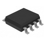
ICGOO电子元器件商城为您提供NTMS4801NR2G由ON Semiconductor设计生产,在icgoo商城现货销售,并且可以通过原厂、代理商等渠道进行代购。 NTMS4801NR2G价格参考。ON SemiconductorNTMS4801NR2G封装/规格:晶体管 - FET,MOSFET - 单, 表面贴装 N 沟道 30V 7.5A(Ta) 800mW(Ta) 8-SOIC。您可以下载NTMS4801NR2G参考资料、Datasheet数据手册功能说明书,资料中有NTMS4801NR2G 详细功能的应用电路图电压和使用方法及教程。
| 参数 | 数值 |
| 产品目录 | |
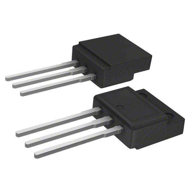
| 描述 | MOSFET N-CH 30V 7.5A 8-SOICMOSFET NFET SO8 30V 9.9A 12.5mOhm |
| 产品分类 | FET - 单分离式半导体 |
| FET功能 | 逻辑电平门 |
| FET类型 | MOSFET N 通道,金属氧化物 |
| Id-连续漏极电流 | 12 A |
| 品牌 | ON Semiconductor |
| 产品手册 | |
| 产品图片 |
|
| rohs | 符合RoHS无铅 / 符合限制有害物质指令(RoHS)规范要求 |
| 产品系列 | 晶体管,MOSFET,ON Semiconductor NTMS4801NR2G- |
| 数据手册 | |
| 产品型号 | NTMS4801NR2G |
| Pd-PowerDissipation | 2.1 W |
| Pd-功率耗散 | 2.1 W |
| RdsOn-漏源导通电阻 | 9 mOhms |
| Vds-漏源极击穿电压 | 30 V |
| Vgs-Gate-SourceBreakdownVoltage | +/- 20 V |
| Vgs-栅源极击穿电压 | 20 V |
| 上升时间 | 3.7 ns |
| 下降时间 | 9.8 ns |
| 不同Id时的Vgs(th)(最大值) | 2.5V @ 250µA |
| 不同Vds时的输入电容(Ciss) | 2201pF @ 25V |
| 不同Vgs时的栅极电荷(Qg) | 25nC @ 10V |
| 不同 Id、Vgs时的 RdsOn(最大值) | 9 毫欧 @ 12A,10V |
| 产品种类 | Logic- Inverters |
| 供应商器件封装 | 8-SOIC N |
| 其它名称 | NTMS4801NR2GOSCT |
| 典型关闭延迟时间 | 29 ns |
| 功率-最大值 | 800mW |
| 功率耗散 | 2.1 W |
| 包装 | 剪切带 (CT) |
| 商标 | ON Semiconductor |
| 安装类型 | 表面贴装 |
| 安装风格 | SMD/SMT |
| 导通电阻 | 9 mOhms |
| 封装 | Reel |
| 封装/外壳 | 8-SOIC(0.154",3.90mm 宽) |
| 封装/箱体 | SOIC-8 Narrow |
| 工厂包装数量 | 2500 |
| 晶体管极性 | N-Channel |
| 最大工作温度 | + 150 C |
| 最小工作温度 | - 55 C |
| 标准包装 | 1 |
| 汲极/源极击穿电压 | 30 V |
| 漏极连续电流 | 12 A |
| 漏源极电压(Vdss) | 30V |
| 电流-连续漏极(Id)(25°C时) | 7.5A (Ta) |
| 系列 | NTMS4801N |
| 通道模式 | Enhancement |
| 配置 | Single Quad Drain Triple Source |
| 闸/源击穿电压 | +/- 20 V |


- 商务部:美国ITC正式对集成电路等产品启动337调查
- 曝三星4nm工艺存在良率问题 高通将骁龙8 Gen1或转产台积电
- 太阳诱电将投资9.5亿元在常州建新厂生产MLCC 预计2023年完工
- 英特尔发布欧洲新工厂建设计划 深化IDM 2.0 战略
- 台积电先进制程称霸业界 有大客户加持明年业绩稳了
- 达到5530亿美元!SIA预计今年全球半导体销售额将创下新高
- 英特尔拟将自动驾驶子公司Mobileye上市 估值或超500亿美元
- 三星加码芯片和SET,合并消费电子和移动部门,撤换高东真等 CEO
- 三星电子宣布重大人事变动 还合并消费电子和移动部门
- 海关总署:前11个月进口集成电路产品价值2.52万亿元 增长14.8%


PDF Datasheet 数据手册内容提取
NTMS4801N MOSFET – Power, N-Channel, SO-8 30 V, 12 A Features • Low R to Minimize Conduction Losses http://onsemi.com DS(on) • Low Capacitance to Minimize Driver Losses • Optimized Gate Charge to Minimize Switching Losses V(BR)DSS RDS(ON) MAX ID MAX • This is a Pb−Free Device 9.0 m(cid:4) @ 10 V 30 V 12 A Applications 12.5 m(cid:4) @ 4.5 V • DC−DC Converters • Synchronous MOSFET N−Channel • Printers D MAXIMUM RATINGS (TJ = 25°C unless otherwise stated) Parameter Symbol Value Unit G Drain−to−Source Voltage VDSS 30 V Gate−to−Source Voltage VGS ±20 V Continuous Drain TA = 25°C ID 9.9 A S Current R(cid:2)JA (Note 1) TA = 70°C 7.9 MARKING DIAGRAM/ Power Dissipation R(cid:2)JA TA = 25°C PD 1.41 W PIN ASSIGNMENT (Note 1) 1 8 Continuous Drain TA = 25°C ID 7.5 A 1 Source Drain CPouwrreenr tD Ris(cid:2)sJiAp a(Ntioonte R 2(cid:2))JA SStetaatdey TTAA == 7205°°CC PD 60..08 W CSATSYSOLE−E 78 1521 SSooGuuarrccteee (cid:2)AYWW(cid:2)4801N DDDrrraaaiiinnn (Note 2) Top View Continuous Drain TA = 25°C ID 12 A Current R(cid:2)JA, t (cid:2) 10 s 4801N = Device Code (Note 1) TA = 70°C 9.6 A = Assembly Location P Ro(cid:2)wJAe,r tD (cid:2)is s1ip0a sti(oNnote 1) TA = 25°C PD 2.1 W YW(cid:2) W === PYWeboa−rrFk rWeee ePkackage Pulsed Drain Current TA = 25°C, tp = 10 (cid:3)s IDM 35 A (Note: Microdot may be in either location) Operating Junction and Storage Temperature TJ, −55 to °C Tstg 150 ORDERING INFORMATION Source Current (Body Diode) IS 2.1 A Device Package Shipping† Single Pulse Drain−to−Source Avalanche Energy EAS 98 mJ (TJ = 25°C, VDD = 30 V, VGS = 10 V, NTMS4801NR2G SO−8 2500/Tape & Reel IL = 14 Apk, L = 1.0 mH, RG = 25 (cid:4)) (Pb−Free) Lead Temperature for Soldering Purposes TL 260 °C †For information on tape and reel specifications, (1/8″ from case for 10 s) including part orientation and tape sizes, please refer to our Tape and Reel Packaging Specification Brochure, BRD8011/D. © Semiconductor Components Industries, LLC, 2009 1 Publication Order Number: June, 2019 − Rev. 2 NTMS4801N/D
NTMS4801N THERMAL RESISTANCE MAXIMUM RATINGS Parameter Symbol Value Unit Junction−to−Ambient – Steady State (Note 1) R(cid:2)JA 88.5 °C/W Junction−to−Ambient – t (cid:2) 10 s (Note 1) R(cid:2)JA 60.5 Junction−to−Foot (Drain) R(cid:2)JF 23 Junction−to−Ambient – Steady State (Note 2) R(cid:2)JA 156 Stresses exceeding Maximum Ratings may damage the device. Maximum Ratings are stress ratings only. Functional operation above the Recommended Operating Conditions is not implied. Extended exposure to stresses above the Recommended Operating Conditions may affect device reliability. 1. Surfacemounted on FR4 board using 1 in sq pad size. 2. Surfacemounted on FR4 board using the minimum recommended pad size. ELECTRICAL CHARACTERISTICS (TJ = 25°C unless otherwise specified) Parameter Symbol Test Condition Min Typ Max Unit OFF CHARACTERISTICS Drain−to−Source Breakdown Voltage V(BR)DSS VGS = 0 V, ID = 250 (cid:3)A 30 V Drain−to−Source Breakdown Voltage V(BR)DSS/TJ 7.0 mV/°C Temperature Coefficient Zero Gate Voltage Drain Current IDSS TJ = 25°C 1.0 (cid:3)A VGS = 0 V, VDS = 24 V TJ = 85°C 10 Gate−to−Source Leakage Current IGSS VDS = 0 V, VGS = ±20 V ±100 nA ON CHARACTERISTICS (Note 3) Gate Threshold Voltage VGS(TH) VGS = VDS, ID = 250 (cid:3)A 1.0 2.5 V Negative Threshold Temperature VGS(TH)/TJ 6.0 mV/°C Coefficient Drain−to−Source On Resistance RDS(on) VGS = 10 V, ID = 12 A 7.0 9.0 m(cid:4) VGS = 4.5 V, ID = 10 A 9.5 12.5 Forward Transconductance gFS VDS = 1.5 V, ID = 12 A 26 S CHARGES, CAPACITANCES AND GATE RESISTANCE Input Capacitance Ciss 1630 2201 pF Output Capacitance Coss VGS = 0 V, f = 1.0 MHz, VDS = 25 V 288 389 Reverse Transfer Capacitance Crss 150 225 Total Gate Charge QG(TOT) 12.2 14 nC Threshold Gate Charge QG(TH) 1.8 VGS = 4.5 V, VDS = 15 V, ID = 12 A Gate−to−Source Charge QGS 5.1 Gate−to−Drain Charge QGD 4.4 Total Gate Charge QG(TOT) VGS = 10 V, VDS = 15 V, ID = 12 A 25 nC SWITCHING CHARACTERISTICS (Note 4) Turn−On Delay Time td(on) 10.5 ns Rise Time tr VGS = 10 V, VDS = 15 V, 3.7 Turn−Off Delay Time td(off) ID = 1.0 A, RG = 6.0 (cid:4) 29 Fall Time tf 9.8 DRAIN−SOURCE DIODE CHARACTERISTICS Forward Diode Voltage VSD TJ = 25°C 0.73 1.0 V VGS = 0 V, IS = 2.1 A TJ = 125°C 0.6 http://onsemi.com 2
NTMS4801N ELECTRICAL CHARACTERISTICS (TJ = 25°C unless otherwise specified) Parameter Symbol Test Condition Min Typ Max Unit DRAIN−SOURCE DIODE CHARACTERISTICS Reverse Recovery Time tRR 22 ns Charge Time ta VGS = 0 V, dIS/dt = 100 A/(cid:3)s, 11 Discharge Time tb IS = 2.1 A 11 Reverse Recovery Charge QRR 13 nC PACKAGE PARASITIC VALUES Source Inductance LS 0.66 nH Drain Inductance LD TA = 25°C 0.20 nH Gate Inductance LG 1.5 nH Gate Resistance RG 1.1 1.8 (cid:4) 3. Pulse Test: pulse width = 300 (cid:3)s, duty cycle (cid:2) 2%. 4. Switching characteristics are independent of operating junction temperatures. http://onsemi.com 3
NTMS4801N TYPICAL PERFORMANCE CURVES 22 22 20 3.4 V to10V 3.2 V TJ = 25°C 20 VDS ≥ 10 V S) 18 S) 18 P P AM 16 AM 16 T ( 14 T ( 14 N N RE 12 3.0 V RE 12 R R U 10 U 10 C C N 8 N 8 DRAI 6 2.8 V DRAI 6 TJ = 100°C D, 4 D, 4 I 2 2.6 V I 2 TJ = 25°C TJ = −55°C 0 0 0 1 2 3 4 5 6 1.5 2 2.5 3 3.5 4 VDS, DRAIN−TO−SOURCE VOLTAGE (VOLTS) VGS, GATE−TO−SOURCE VOLTAGE (VOLTS) Figure 1. On−Region Characteristics Figure 2. Transfer Characteristics (cid:4)) (cid:4)) E ( 0.050 E ( 0.016 NC 0.045 TJ = 25°C NC TJ = 25°C STA 0.040 ID = 12 A STA 0.014 SI SI E 0.035 E R R 0.012 E 0.030 E VGS = 4.5 V C C R R U 0.025 U 0.01 O O S 0.020 S − − O O 0.008 T 0.015 T N− N− VGS = 10 V AI 0.010 AI 0.006 R R D 0.005 D on), 0 on), 0.004 S( 2 4 6 8 10 S( 2 4 6 8 10 12 14 16 18 20 22 D D R R VGS, GATE−TO−SOURCE VOLTAGE (VOLTS) ID, DRAIN CURRENT (AMPS) Figure 3. On−Resistance vs. Gate−to−Source Figure 4. On−Resistance vs. Drain Current and Voltage Gate Voltage 1.8 100000 VGS = 10 V VGS = 0 V ED) 1.6 ID = 12 A CE O−SOURRMALIZ 1.4 GE (nA) 10000 TJ = 150°C TO A −N 1.2 K DRAIN S(on),SISTANCE ( 1.0 I, LEADSS 1000 TJ = 125°C DE 0.8 RR 0.6 100 −50 −25 0 25 50 75 100 125 150 5 10 15 20 25 30 TJ, JUNCTION TEMPERATURE (°C) VDS, DRAIN−TO−SOURCE VOLTAGE (VOLTS) Figure 5. On−Resistance Variation with Figure 6. Drain−to−Source Leakage Current Temperature vs. Voltage http://onsemi.com 4
NTMS4801N TYPICAL PERFORMANCE CURVES 2500 10 20 TJ = 25°C OLTS) QT 18DSV E (pF) 2000 Ciss VGS = 0 V OLTAGE (V 8 VDS VGS 1164, DRAIN-TO C 1500 V 6 12- PACITAN 1000 -SOURCE 4 QGS QGD 810SOURCE V C, CA 500 Coss , GATE-TOS 2 ID = 12 A 462 OLTAGE (VO Crss VG TJ = 25°C LT 0 0 0 S ) 0 5 10 15 20 25 30 0 5 10 15 20 25 30 DRAIN−TO−SOURCE VOLTAGE (VOLTS) QG, TOTAL GATE CHARGE (nC) Figure 7. Capacitance Variation Figure 8. Gate−To−Source and Drain−To−Source Voltage vs. Total Charge 1000 4 VIDD =D 1= A15 V PS) VTJG =S =2 50° CV VGS = 10 V td(off) AM 3 100 T ( s) tf EN n R t, TIME ( 10 ttdr(on) CE CUR 2 R U O 1 S , S I 1 0 1 10 100 0.5 0.55 0.6 0.65 0.7 0.75 0.8 RG, GATE RESISTANCE (OHMS) VSD, SOURCE−TO−DRAIN VOLTAGE (VOLTS) Figure 9. Resistive Switching Time Figure 10. Diode Forward Voltage vs. Current Variation vs. Gate Resistance 100 E 100 C UR ID = 14 A S) 10 (cid:3)s O RENT (AMP 10 110 0m (cid:3)ss RAIN−TO−SNERGY (mJ) 75 R 1 DE 50 DRAIN CU 0.1 VSTCGIN S=G =2L 52E°0 CP VULSE 10 ms E PULSE LANCHE 25 I, D RTHDSE(RonM) ALILM LITIMIT dc SINGLAVA 0.01 PACKAGE LIMIT AS, 0 0.1 1 10 100 E 25 50 75 100 125 150 VDS, DRAIN−TO−SOURCE VOLTAGE (VOLTS) TJ, STARTING JUNCTION TEMPERATURE (°C) Figure 11. Maximum Rated Forward Biased Figure 12. Maximum Avalanche Energy vs. Safe Operating Area Starting Junction Temperature http://onsemi.com 5
NTMS4801N PACKAGE DIMENSIONS SOIC−8 CASE 751−07 ISSUE AJ −X− NOTES: 1. DIMENSIONING AND TOLERANCING PER A ANSI Y14.5M, 1982. 2. CONTROLLING DIMENSION: MILLIMETER. 3. DIMENSION A AND B DO NOT INCLUDE MOLD PROTRUSION. 8 5 4. MAXIMUM MOLD PROTRUSION 0.15 (0.006) PER SIDE. B S 0.25 (0.010) M Y M 5. DIMENSION D DOES NOT INCLUDE DAMBAR PROTRUSION. ALLOWABLE DAMBAR 1 PROTRUSION SHALL BE 0.127 (0.005) TOTAL −Y− 4 K IMNA EXXIMCUEMSS M OAFT ETRHIEA LD CDOIMNEDNITSIOIONN. AT 6. 751−01 THRU 751−06 ARE OBSOLETE. NEW STANDARD IS 751−07. G MILLIMETERS INCHES C NX 45(cid:3) DIM MIN MAX MIN MAX A 4.80 5.00 0.189 0.197 SEATING PLANE B 3.80 4.00 0.150 0.157 −Z− C 1.35 1.75 0.053 0.069 D 0.33 0.51 0.013 0.020 0.10 (0.004) G 1.27 BSC 0.050 BSC H D M J H 0.10 0.25 0.004 0.010 J 0.19 0.25 0.007 0.010 K 0.40 1.27 0.016 0.050 0.25 (0.010)M Z Y S X S M 0 (cid:3) 8 (cid:3) 0 (cid:3) 8 (cid:3) N 0.25 0.50 0.010 0.020 S 5.80 6.20 0.228 0.244 SOLDERING FOOTPRINT* STYLE 12: PIN 1. SOURCE 2. SOURCE 3. SOURCE 4. GATE 1.52 5. DRAIN 0.060 6. DRAIN 7. DRAIN 8. DRAIN 7.0 4.0 0.275 0.155 0.6 1.270 0.024 0.050 (cid:3) (cid:4) mm SCALE 6:1 inches *For additional information on our Pb−Free strategy and soldering details, please download the ON Semiconductor Soldering and Mounting Techniques Reference Manual, SOLDERRM/D. ON Semiconductor and are registered trademarks of Semiconductor Components Industries, LLC (SCILLC). SCILLC reserves the right to make changes without further notice to any products herein. SCILLC makes no warranty, representation or guarantee regarding the suitability of its products for any particular purpose, nor does SCILLC assume any liability arising out of the application or use of any product or circuit, and specifically disclaims any and all liability, including without limitation special, consequential or incidental damages. “Typical” parameters which may be provided in SCILLC data sheets and/or specifications can and do vary in different applications and actual performance may vary over time. All operating parameters, including “Typicals” must be validated for each customer application by customer’s technical experts. SCILLC does not convey any license under its patent rights nor the rights of others. SCILLC products are not designed, intended, or authorized for use as components in systems intended for surgical implant into the body, or other applications intended to support or sustain life, or for any other application in which the failure of the SCILLC product could create a situation where personal injury or death may occur. Should Buyer purchase or use SCILLC products for any such unintended or unauthorized application, Buyer shall indemnify and hold SCILLC and its officers, employees, subsidiaries, affiliates, and distributors harmless against all claims, costs, damages, and expenses, and reasonable attorney fees arising out of, directly or indirectly, any claim of personal injury or death associated with such unintended or unauthorized use, even if such claim alleges that SCILLC was negligent regarding the design or manufacture of the part. SCILLC is an Equal Opportunity/Affirmative Action Employer. This literature is subject to all applicable copyright laws and is not for resale in any manner. PUBLICATION ORDERING INFORMATION LITERATURE FULFILLMENT: N. American Technical Support: 800−282−9855 Toll Free ON Semiconductor Website: www.onsemi.com Literature Distribution Center for ON Semiconductor USA/Canada P.O. Box 5163, Denver, Colorado 80217 USA Europe, Middle East and Africa Technical Support: Order Literature: http://www.onsemi.com/orderlit Phone: 303−675−2175 or 800−344−3860 Toll Free USA/Canada Phone: 421 33 790 2910 Fax: 303−675−2176 or 800−344−3867 Toll Free USA/Canada Japan Customer Focus Center For additional information, please contact your local Email: orderlit@onsemi.com Phone: 81−3−5773−3850 Sales Representative http://onsemi.com NTMS4801N/D 6