ICGOO在线商城 > 分立半导体产品 > 晶体管 - FET,MOSFET - 单 > NTD3055-094-1G

 Datasheet下载
- 型号: NTD3055-094-1G
- 制造商: ON Semiconductor
- 库位|库存: xxxx|xxxx
- 要求:
| 数量阶梯 | 香港交货 | 国内含税 |
| +xxxx | $xxxx | ¥xxxx |
查看当月历史价格
查看今年历史价格
NTD3055-094-1G产品简介:
ICGOO电子元器件商城为您提供NTD3055-094-1G由ON Semiconductor设计生产,在icgoo商城现货销售,并且可以通过原厂、代理商等渠道进行代购。 NTD3055-094-1G价格参考。ON SemiconductorNTD3055-094-1G封装/规格:晶体管 - FET,MOSFET - 单, 通孔 N 沟道 60V 12A(Ta) 1.5W(Ta),48W(Tj) I-PAK。您可以下载NTD3055-094-1G参考资料、Datasheet数据手册功能说明书,资料中有NTD3055-094-1G 详细功能的应用电路图电压和使用方法及教程。
ON Semiconductor的NTD3055-094-1G是一款N沟道增强型MOSFET(金属氧化物场效应晶体管),广泛应用于多种电力电子设备中。该型号的主要应用场景包括:

 1. 电源管理
   NTD3055-094-1G常用于开关电源(SMPS)、DC-DC转换器和线性稳压器等电源管理系统中。它能够高效地控制电流的开关,减少能量损耗,提升电源转换效率。其低导通电阻(Rds(on))特性使其在高频开关应用中表现出色,特别适合需要高能效的应用场景。

 2. 电机驱动
   在电机驱动电路中,NTD3055-094-1G可以作为功率级元件,用于控制电机的启动、停止和调速。它的快速开关特性和低功耗特点使其适用于小型直流电机、步进电机和无刷直流电机(BLDC)的驱动电路中。

 3. 负载开关
   该MOSFET可以用作负载开关,控制不同负载之间的电源分配。例如,在便携式设备、消费电子产品和工业控制系统中,NTD3055-094-1G可以实现对不同模块或子系统的电源管理,确保系统在待机或关机状态下消耗尽可能少的电流。

 4. 电池保护
   在电池管理系统(BMS)中,NTD3055-094-1G可以用于电池充放电保护电路。它可以在过流、过压或短路等异常情况下迅速切断电流路径,保护电池和相关电路免受损坏。

 5. 逆变器和变频器
   在逆变器和变频器中,NTD3055-094-1G可以用于将直流电转换为交流电,或者调节输出电压和频率。其良好的热稳定性和耐压能力使其能够在这些高要求的应用中保持可靠运行。

 6. 汽车电子
   在汽车电子领域,NTD3055-094-1G可用于车载充电器、电动助力转向系统(EPS)、LED照明驱动等应用。它能够承受汽车环境中常见的温度变化和电压波动,确保系统的稳定性和安全性。

总之,NTD3055-094-1G凭借其优异的电气性能和可靠性,适用于多种电力电子应用,尤其在需要高效、低功耗和快速响应的场合中表现突出。
| 参数 | 数值 |
| 产品目录 | |
| 描述 | MOSFET N-CH 60V 12A IPAKMOSFET 60V 12A N-Channel |
| 产品分类 | FET - 单分离式半导体 |
| FET功能 | 标准 |
| FET类型 | MOSFET N 通道,金属氧化物 |
| Id-连续漏极电流 | 12 A |
| 品牌 | ON Semiconductor |
| 产品手册 | |
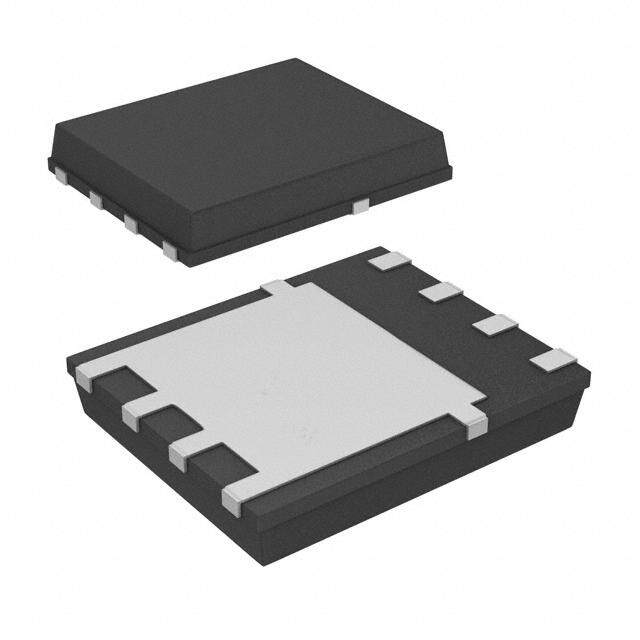
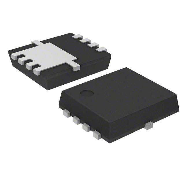
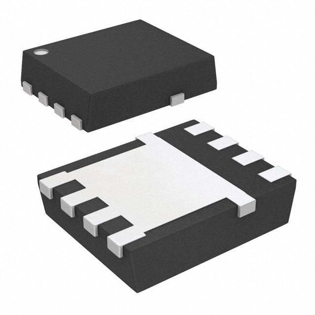
| 产品图片 |
|
| rohs | 符合RoHS无铅 / 符合限制有害物质指令(RoHS)规范要求 |
| 产品系列 | 晶体管,MOSFET,ON Semiconductor NTD3055-094-1G- |
| 数据手册 | |
| 产品型号 | NTD3055-094-1G |
| Pd-PowerDissipation | 48 W |
| Pd-功率耗散 | 48 W |
| RdsOn-漏源导通电阻 | 94 mOhms |
| Vds-漏源极击穿电压 | 60 V |
| Vgs-Gate-SourceBreakdownVoltage | +/- 20 V |
| Vgs-栅源极击穿电压 | 20 V |
| 上升时间 | 32.3 ns |
| 下降时间 | 23.9 ns |
| 不同Id时的Vgs(th)(最大值) | 4V @ 250µA |
| 不同Vds时的输入电容(Ciss) | 450pF @ 25V |
| 不同Vgs时的栅极电荷(Qg) | 20nC @ 10V |
| 不同 Id、Vgs时的 RdsOn(最大值) | 94 毫欧 @ 6A,10V |
| 产品种类 | MOSFETs- Power and Small Signal |
| 供应商器件封装 | I-Pak |
| 其它名称 | NTD3055-094-1G-ND |
| 典型关闭延迟时间 | 25.2 ns |
| 功率-最大值 | 1.5W |
| 包装 | 管件 |
| 商标 | ON Semiconductor |
| 安装类型 | 通孔 |
| 安装风格 | SMD/SMT |
| 导通电阻 | 94 mOhms |
| 封装 | Tube |
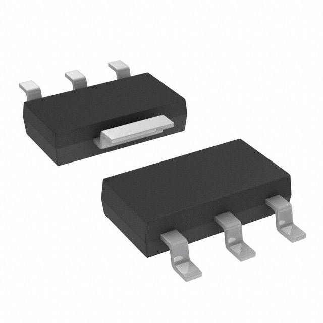
| 封装/外壳 | TO-251-3 短引线,IPak,TO-251AA |
| 封装/箱体 | DPAK-SL |
| 工厂包装数量 | 75 |
| 晶体管极性 | N-Channel |
| 最大工作温度 | + 175 C |
| 最小工作温度 | - 55 C |
| 标准包装 | 75 |
| 正向跨导-最小值 | 6.7 S |
| 汲极/源极击穿电压 | 60 V |
| 漏极连续电流 | 12 A |
| 漏源极电压(Vdss) | 60V |
| 电流-连续漏极(Id)(25°C时) | 12A (Ta) |
| 系列 | NTD3055-094 |
| 通道模式 | Enhancement |
| 配置 | Single |


- 商务部:美国ITC正式对集成电路等产品启动337调查
- 曝三星4nm工艺存在良率问题 高通将骁龙8 Gen1或转产台积电
- 太阳诱电将投资9.5亿元在常州建新厂生产MLCC 预计2023年完工
- 英特尔发布欧洲新工厂建设计划 深化IDM 2.0 战略
- 台积电先进制程称霸业界 有大客户加持明年业绩稳了
- 达到5530亿美元!SIA预计今年全球半导体销售额将创下新高
- 英特尔拟将自动驾驶子公司Mobileye上市 估值或超500亿美元
- 三星加码芯片和SET,合并消费电子和移动部门,撤换高东真等 CEO
- 三星电子宣布重大人事变动 还合并消费电子和移动部门
- 海关总署:前11个月进口集成电路产品价值2.52万亿元 增长14.8%


PDF Datasheet 数据手册内容提取
NTD3055-094, NVD3055-094 Power MOSFET 12 A, 60 V, N−Channel DPAK/IPAK Designed for low voltage, high speed switching applications in power supplies, converters and power motor controls and bridge circuits. Features • Lower R http://onsemi.com DS(on) • Lower V DS(on) • Lower and Tighter V V(BR)DSS RDS(on) TYP ID MAX SD • Lower Diode Reverse Recovery Time 60 V 94 m(cid:2) 12 A • Lower Reverse Recovery Stored Charge • D NVD Prefix for Automotive and Other Applications Requiring Unique Site and Control Change Requirements; AEC−Q101 Qualified and PPAP Capable • N−Channel These Devices are Pb−Free and are RoHS Compliant G Typical Applications • Power Supplies S • Converters 4 • Power Motor Controls • Bridge Circuits 4 MAXIMUM RATINGS (TJ = 25°C unless otherwise noted) 1 2 12 Rating Symbol Value Unit 3 3 Drain−to−Source Voltage VDSS 60 Vdc DPAK IPAK Drain−to−Gate Voltage (RGS = 10 M(cid:2)) VDGR 60 Vdc CASE 369C CASE 369D STYLE 2 STYLE 2 Gate−to−Source Voltage Vdc − Continuous VGS (cid:3)20 − Non−Repetitive (tp(cid:2)10 ms) VGS (cid:3)30 MARKING DIAGRAM & PIN ASSIGNMENTS Drain Current − Continuous @ TA = 25°C ID 12 Adc 4 4 − Continuous @ TA = 100°C ID 10 Drain Drain − Single Pulse (tp(cid:2)10 (cid:3)s) IDM 45 Apk Total Power Dissipation @ TA = 25°C PD 48 W W W G ToDtael rPaotew aebr oDvises 2ip5a°tCion @ TA = 25°C (Note 1) 02..312 WW/°C AYW55094G AYW553094 Total Power Dissipation @ TA = 25°C (Note 2) 1.5 W Operating and Storage Temperature Range TJ, Tstg −55 to °C 1 2 3 +175 Drain Gate Source 1 2 3 Single Pulse Drain−to−Source Avalanche EAS 61 mJ Energy − Starting TJ = 25°C Gate Drain Source (VDD = 25 Vdc, VGS = 10 Vdc, L = 1.0 mH A = Assembly Location* IL(pk) = 11 A, VDS = 60 Vdc) 55094 = Device Code Thermal Resistance Y = Year − Junction−to−Case R(cid:4)JC 3.13 °C/W WW = Work Week − Junction−to−Ambient (Note 1) R(cid:4)JA 71.4 G = Pb−Free Package − Junction−to−Ambient (Note 2) R(cid:4)JA 100 Maximum Lead Temperature for Soldering TL 260 °C * The Assembly Location code (A) is front side Purposes, 1/8″ from case for 10 seconds optional. In cases where the Assembly Location is stamped in the package, the front side assembly Stresses exceeding those listed in the Maximum Ratings table may damage the code may be blank. device. If any of these limits are exceeded, device functionality should not be assumed, damage may occur and reliability may be affected. 1. When surface mounted to an FR4 board using 0.5 sq in. pad size. ORDERING INFORMATION 2. When surface mounted to an FR4 board using the minimum recommended See detailed ordering and shipping information in the package pad size. dimensions section on page 7 of this data sheet. © Semiconductor Components Industries, LLC, 2014 1 Publication Order Number: July, 2014 − Rev. 9 NTD3055−094/D
NTD3055−094, NVD3055−094 ELECTRICAL CHARACTERISTICS (TJ = 25°C unless otherwise noted) Characteristic Symbol Min Typ Max Unit OFF CHARACTERISTICS Drain−to−Source Breakdown Voltage (Note 3) V(BR)DSS Vdc (VGS = 0 Vdc, ID = 250 (cid:3)Adc) 60 68 − Temperature Coefficient (Positive) − 54.4 − mV/°C Zero Gate Voltage Drain Current IDSS (cid:3)Adc (VDS = 60 Vdc, VGS = 0 Vdc) − − 1.0 (VDS = 60 Vdc, VGS = 0 Vdc, TJ = 150°C) − − 10 Gate−Body Leakage Current (VGS = ±20 Vdc, VDS = 0 Vdc) IGSS − − ±100 nAdc ON CHARACTERISTICS (Note 3) Gate Threshold Voltage (Note 3) VGS(th) Vdc (VDS = VGS, ID = 250 (cid:3)Adc) 2.0 2.9 4.0 Threshold Temperature Coefficient (Negative) − 6.3 − mV/°C Static Drain−to−Source On−Resistance (Note 3) RDS(on) m(cid:2) (VGS = 10 Vdc, ID = 6.0 Adc) − 84 94 Static Drain−to−Source On−Voltage (Note 3) VDS(on) Vdc (VGS = 10 Vdc, ID = 12 Adc) − 0.85 1.35 (VGS = 10 Vdc, ID = 6.0 Adc, TJ = 150°C) − 0.77 − Forward Transconductance (Note 3) (VDS = 7.0 Vdc, ID = 6.0 Adc) gFS − 6.7 − mhos DYNAMIC CHARACTERISTICS Input Capacitance Ciss − 323 450 pF Output Capacitance (VDS = 2f5 = V 1d.c0, MVHGSz) = 0 Vdc, Coss − 107 150 Transfer Capacitance Crss − 34 70 SWITCHING CHARACTERISTICS (Note 4) Turn−On Delay Time td(on) − 7.7 15 ns Rise Time (VDD = 48 Vdc, ID = 12 Adc, tr − 32.3 70 Turn−Off Delay Time VGS = 10 Vdc, RG = 9.1 (cid:2)) (Note 3) td(off) − 25.2 50 Fall Time tf − 23.9 50 Gate Charge QT − 10.9 20 nC (VDVSG S= =4 81 0V dVcd,c I)D ( N= o1t2e A3)dc, Q1 − 3.1 − Q2 − 4.2 − SOURCE−DRAIN DIODE CHARACTERISTICS Forward On−Voltage (IS = 12 Adc, VGS = 0 Vdc) (Note 3) VSD − 0.94 1.15 Vdc (IS = 12 Adc, VGS = 0 Vdc, TJ = 150°C) − 0.82 − Reverse Recovery Time trr − 33.1 − ns (dIISS /=d t1 =2 1A0d0c ,A V/(cid:3)GsS) =(N 0o tVed 3c), ta − 24 − tb − 8.9 − Reverse Recovery Stored Charge QRR − 0.047 − (cid:3)C Product parametric performance is indicated in the Electrical Characteristics for the listed test conditions, unless otherwise noted. Product performance may not be indicated by the Electrical Characteristics if operated under different conditions. 3. Pulse Test: Pulse Width ≤300 (cid:3)s, Duty Cycle ≤ 2%. 4. Switching characteristics are independent of operating junction temperatures. http://onsemi.com 2
NTD3055−094, NVD3055−094 TYPICAL CHARACTERISTICS 24 24 VGS = 10 V 7 V VDS ≥ 10 V PS) 20 9 V 6.5 V PS) 20 M M A 8 V A T ( 16 T ( 16 N 6 V N E E R R R 12 R 12 U 5.5 V U C C N N RAI 8 5 V RAI 8 TJ = 25°C D D I, D 4 4.5 V I, D 4 TJ = 100°C TJ = −55°C 0 0 0 1 2 3 4 5 3 3.5 4 4.5 5 5.5 6 6.5 7 7.5 8 VDS, DRAIN−TO−SOURCE VOLTAGE (VOLTS) VGS, GATE−TO−SOURCE VOLTAGE (VOLTS) Figure 1. On−Region Characteristics Figure 2. Transfer Characteristics (cid:2)) (cid:2)) CE ( 0.20 CE ( 0.20 N N TA 0.18 VGS = 10 V TA 0.18 VGS = 15 V RESIS 00..1146 TJ = 100°C RESIS 00..1164 RCE 0.12 RCE 0.12 TJ = 100°C OU 0.10 OU 0.10 O−S 0.08 TJ = 25°C O−S 0.08 TJ = 25°C T T RAIN− 00..0046 TJ = −55°C RAIN− 00..0046 TJ = −55°C D D , DS(on) 0.0020 4 8 12 16 20 24 , DS(on) 0.0020 4 8 12 16 20 24 R R ID, DRAIN CURRENT (AMPS) ID, DRAIN CURRENT (AMPS) Figure 3. On−Resistance versus Figure 4. On−Resistance versus Drain Current Gate−to−Source Voltage and Gate Voltage CE 2 1000 TAN 1.8 ID = 6 A VGS = 0 V TJ = 150°C SIS VGS = 10 V RE 1.6 A) RCE ZED)1.4 GE (n 100 N−TO−SOU(NORMALI1.12 , LEAKADSS 10 TJ = 100°C AI I R D 0.8 , n) S(o 0.6 1 RD −50 −25 0 25 50 75 100 125 150 175 0 10 20 30 40 50 60 TJ, JUNCTION TEMPERATURE (°C) VDS, DRAIN−TO−SOURCE VOLTAGE (VOLTS) Figure 5. On−Resistance Variation with Figure 6. Drain−to−Source Leakage Current Temperature versus Voltage http://onsemi.com 3
NTD3055−094, NVD3055−094 POWER MOSFET SWITCHING Switching behavior is most easily modeled and predicted The capacitance (C ) is read from the capacitance curve at iss by recognizing that the power MOSFET is charge a voltage corresponding to the off−state condition when controlled. The lengths of various switching intervals ((cid:5)t) calculating t and is read at a voltage corresponding to the d(on) are determined by how fast the FET input capacitance can on−state when calculating t . d(off) be charged by current from the generator. At high switching speeds, parasitic circuit elements complicate the analysis. The inductance of the MOSFET The published capacitance data is difficult to use for source lead, inside the package and in the circuit wiring calculating rise and fall because drain−gate capacitance which is common to both the drain and gate current paths, varies greatly with applied voltage. Accordingly, gate produces a voltage at the source which reduces the gate drive charge data is used. In most cases, a satisfactory estimate of current. The voltage is determined by Ldi/dt, but since di/dt average input current (I ) can be made from a G(AV) is a function of drain current, the mathematical solution is rudimentary analysis of the drive circuit so that complex. The MOSFET output capacitance also t = Q/I G(AV) complicates the mathematics. And finally, MOSFETs have During the rise and fall time interval when switching a finite internal gate resistance which effectively adds to the resistive load, V remains virtually constant at a level resistance of the driving source, but the internal resistance GS known as the plateau voltage, V . Therefore, rise and fall is difficult to measure and, consequently, is not specified. SGP times may be approximated by the following: The resistive switching time variation versus gate resistance (Figure 9) shows how typical switching t = Q x R /(V − V ) r 2 G GG GSP performance is affected by the parasitic circuit elements. If t = Q x R /V f 2 G GSP the parasitics were not present, the slope of the curves would where maintain a value of unity regardless of the switching speed. The circuit used to obtain the data is constructed to minimize V = the gate drive voltage, which varies from zero to V GG GG common inductance in the drain and gate circuit loops and R = the gate drive resistance G is believed readily achievable with board mounted and Q2 and VGSP are read from the gate charge curve. components. Most power electronic loads are inductive; the data in the figure is taken with a resistive load, which During the turn−on and turn−off delay times, gate current is approximates an optimally snubbed inductive load. Power not constant. The simplest calculation uses appropriate MOSFETs may be safely operated into an inductive load; values from the capacitance curves in a standard equation for however, snubbing reduces switching losses. voltage change in an RC network. The equations are: td(on) = RG Ciss In [VGG/(VGG − VGSP)] t = R C In (V /V ) d(off) G iss GG GSP 800 VDS = 0 V VGS = 0 V Ciss TJ = 25°C F) 600 p E ( C N TA 400 Crss CI A P A Ciss C C, 200 Coss 0 Crss 10 5 0 5 10 15 20 25 VGS VDS GATE−TO−SOURCE OR DRAIN−TO−SOURCE VOLTAGE (VOLTS) Figure 7. Capacitance Variation http://onsemi.com 4
NTD3055−094, NVD3055−094 S) 12 100 T OL QT V 10 GE ( VGS E VOLTA 86 Q1 Q2 ME (ns) 10 td(ottfrff) OURC 4 t, TI td(on) S TE−TO− 2 ITDJ == 1225 °AC VIVDDG =SS 1==2 31 A00 VV GA 0 1 , S 0 2 4 6 8 10 12 1 10 100 VG QG, TOTAL GATE CHARGE (nC) RG, GATE RESISTANCE (OHMS) Figure 8. Gate−To−Source and Drain−To−Source Figure 9. Resistive Switching Time Voltage versus Total Charge Variation versus Gate Resistance DRAIN−TO−SOURCE DIODE CHARACTERISTICS 16 PS) 14 VTJG =S =2 50° CV M A 12 T ( EN 10 R R U 8 C CE 6 R U O 4 S , S 2 I 0 0.6 0.68 0.76 0.84 0.92 1 VSD, SOURCE−TO−DRAIN VOLTAGE (VOLTS) Figure 10. Diode Forward Voltage versus Current SAFE OPERATING AREA The Forward Biased Safe Operating Area curves define reliable operation, the stored energy from circuit inductance the maximum simultaneous drain−to−source voltage and dissipated in the transistor while in avalanche must be less drain current that a transistor can handle safely when it is than the rated limit and adjusted for operating conditions forward biased. Curves are based upon maximum peak differing from those specified. Although industry practice is junction temperature and a case temperature (T ) of 25°C. to rate in terms of energy, avalanche energy capability is not C Peak repetitive pulsed power limits are determined by using a constant. The energy rating decreases non−linearly with an the thermal response data in conjunction with the procedures increase of peak current in avalanche and peak junction discussed in AN569, “Transient Thermal Resistance − temperature. General Data and Its Use.” Although many E−FETs can withstand the stress of Switching between the off−state and the on−state may drain−to−source avalanche at currents up to rated pulsed traverse any load line provided neither rated peak current current (I ), the energy rating is specified at rated DM (I ) nor rated voltage (V ) is exceeded and the continuous current (I ), in accordance with industry custom. DM DSS D transition time (t,t) do not exceed 10 (cid:3)s. In addition the total The energy rating must be derated for temperature as shown r f power averaged over a complete switching cycle must not in the accompanying graph (Figure 12). Maximum energy at exceed (TJ(MAX) − TC)/(R(cid:4)JC). currents below rated continuous ID can safely be assumed to A Power MOSFET designated E−FET can be safely used equal the values indicated. in switching circuits with unclamped inductive loads. For http://onsemi.com 5
NTD3055−094, NVD3055−094 SAFE OPERATING AREA 100 E 70 C PS) VSIGNSG =L 2E0 P VU LSE 10 (cid:3)s OUR 60 ID = 11 A T (AM 10 TC = 25°C TO−SmJ) 5500 EN N−Y ( RR 100 (cid:3)s RAIRG 40 U DE AIN C 1 1 ms ULSE HE EN 30 R 10 ms dc PC 20 , DD RDS(on) LIMIT LE AN I THERMAL LIMIT NGAL 10 PACKAGE LIMIT SIAV 0.1 , S 0 0.1 1 10 100 A 25 50 75 100 125 150 175 E VDS, DRAIN−TO−SOURCE VOLTAGE (VOLTS) TJ, STARTING JUNCTION TEMPERATURE (°C) Figure 11. Maximum Rated Forward Biased Figure 12. Maximum Avalanche Energy versus Safe Operating Area Starting Junction Temperature E C N A T S 1.0 SI E D = 0.5 R L A RMD) 0.2 THELIZE 0.1 NT MA 0.1 0.05 P(pk) SIENOR 0.02 RD (cid:4)CJCU(Rt)V =E rS(t )A RP(cid:4)PJLCY FOR POWER AN( PULSE TRAIN SHOWN R T 0.01 t1 READ TIME AT t1 VE SINGLE PULSE t2 TJ(pk) - TC = P(pk) R(cid:4)JC(t) TI DUTY CYCLE, D = t1/t2 C FE 0.01 F 0.00001 0.0001 0.001 0.01 0.1 1 10 E r(t), t, TIME ((cid:3)s) Figure 13. Thermal Response di/dt IS trr ta tb TIME tp 0.25 IS IS Figure 14. Diode Reverse Recovery Waveform http://onsemi.com 6
NTD3055−094, NVD3055−094 ORDERING INFORMATION Device Package Shipping† NTD3055−094−1G IPAK 75 Units / Rail (Pb−Free) NTD3055−094T4G DPAK 2500 / Tape & Reel (Pb−Free) NVD3055−094T4G* DPAK 2500 / Tape & Reel (Pb−Free) †For information on tape and reel specifications, including part orientation and tape sizes, please refer to our Tape and Reel Packaging Specifications Brochure, BRD8011/D. *NVD Prefix for Automotive and Other Applications Requiring Unique Site and Control Change Requirements; AEC−Q101 Qualified and PPAP Capable. http://onsemi.com 7
NTD3055−094, NVD3055−094 PACKAGE DIMENSIONS DPAK (SINGLE GAUGE) CASE 369C ISSUE E NOTES: A 1.DIMENSIONING AND TOLERANCING PER ASME Y14.5M, 1994. E C 2.CONTROLLING DIMENSION: INCHES. A 3.THERMAL PAD CONTOUR OPTIONAL WITHIN DI- b3 B MENSIONS b3, L3 and Z. c2 4.DIMENSIONS D AND E DO NOT INCLUDE MOLD FLASH, PROTRUSIONS, OR BURRS. MOLD FLASH, PROTRUSIONS, OR GATE BURRS SHALL 4 NOT EXCEED 0.006 INCHES PER SIDE. L3 Z Z 5.DIMENSIONS D AND E ARE DETERMINED AT THE D DETAIL A H 6.DOAUTTUEMRSM OA SATN EDX BT RAERME EDSE OTEFR TMHIEN EPDLA ASTT DICA TBUOMDY. 1 2 3 PLANE H. 7.OPTIONAL MOLD FEATURE. L4 INCHES MILLIMETERS NOTE 7 b2 c BOTTOM VIEW BOTTOM VIEW DIM MIN MAX MIN MAX A 0.086 0.094 2.18 2.38 e SIDE VIEW ALTERNATE A1 0.000 0.005 0.00 0.13 b CONSTRUCTION b 0.025 0.035 0.63 0.89 0.005 (0.13) M C H b2 0.028 0.045 0.72 1.14 TOP VIEW b3 0.180 0.215 4.57 5.46 c 0.018 0.024 0.46 0.61 L2 GPLAAUNGEE C SPELAATNIENG cD2 00..203158 00..204254 50..9476 60..2621 E 0.250 0.265 6.35 6.73 e 0.090 BSC 2.29 BSC L H 0.370 0.410 9.40 10.41 A1 L 0.055 0.070 1.40 1.78 L1 L1 0.114 REF 2.90 REF DETAIL A L2 0.020 BSC 0.51 BSC ROTATED 90(cid:2) CW L3 0.035 0.050 0.89 1.27 L4 −−− 0.040 −−− 1.01 Z 0.155 −−− 3.93 −−− STYLE 2: SOLDERING FOOTPRINT* PIN 1.GATE 2.DRAIN 3.SOURCE 6.20 3.00 4.DRAIN 0.244 0.118 2.58 0.102 5.80 1.60 6.17 0.228 0.063 0.243 (cid:4) (cid:5) mm SCALE 3:1 inches *For additional information on our Pb−Free strategy and soldering details, please download the ON Semiconductor Soldering and Mounting Techniques Reference Manual, SOLDERRM/D. http://onsemi.com 8
NTD3055−094, NVD3055−094 PACKAGE DIMENSIONS IPAK CASE 369D ISSUE C B C NOTES: 1. DIMENSIONING AND TOLERANCING PER V R E ANSI Y14.5M, 1982. 2. CONTROLLING DIMENSION: INCH. INCHES MILLIMETERS 4 Z DIM MIN MAX MIN MAX A 0.235 0.245 5.97 6.35 A S B 0.250 0.265 6.35 6.73 1 2 3 C 0.086 0.094 2.19 2.38 D 0.027 0.035 0.69 0.88 E 0.018 0.023 0.46 0.58 −T− F 0.037 0.045 0.94 1.14 SEATING G 0.090 BSC 2.29 BSC PLANE K H 0.034 0.040 0.87 1.01 J 0.018 0.023 0.46 0.58 K 0.350 0.380 8.89 9.65 R 0.180 0.215 4.45 5.45 F J S 0.025 0.040 0.63 1.01 H V 0.035 0.050 0.89 1.27 Z 0.155 −−− 3.93 −−− D 3 PL STYLE 2: G 0.13 (0.005) M T PIN 1. GATE 2. DRAIN 3. SOURCE 4. DRAIN ON Semiconductor and the are registered trademarks of Semiconductor Components Industries, LLC (SCILLC) or its subsidiaries in the United States and/or other countries. SCILLC owns the rights to a number of patents, trademarks, copyrights, trade secrets, and other intellectual property. A listing of SCILLC’s product/patent coverage may be accessed at www.onsemi.com/site/pdf/Patent−Marking.pdf. SCILLC reserves the right to make changes without further notice to any products herein. SCILLC makes no warranty, representation or guarantee regarding the suitability of its products for any particular purpose, nor does SCILLC assume any liability arising out of the application or use of any product or circuit, and specifically disclaims any and all liability, including without limitation special, consequential or incidental damages. “Typical” parameters which may be provided in SCILLC data sheets and/or specifications can and do vary in different applications and actual performance may vary over time. All operating parameters, including “Typicals” must be validated for each customer application by customer’s technical experts. SCILLC does not convey any license under its patent rights nor the rights of others. SCILLC products are not designed, intended, or authorized for use as components in systems intended for surgical implant into the body, or other applications intended to support or sustain life, or for any other application in which the failure of the SCILLC product could create a situation where personal injury or death may occur. Should Buyer purchase or use SCILLC products for any such unintended or unauthorized application, Buyer shall indemnify and hold SCILLC and its officers, employees, subsidiaries, affiliates, and distributors harmless against all claims, costs, damages, and expenses, and reasonable attorney fees arising out of, directly or indirectly, any claim of personal injury or death associated with such unintended or unauthorized use, even if such claim alleges that SCILLC was negligent regarding the design or manufacture of the part. SCILLC is an Equal Opportunity/Affirmative Action Employer. This literature is subject to all applicable copyright laws and is not for resale in any manner. PUBLICATION ORDERING INFORMATION LITERATURE FULFILLMENT: N. American Technical Support: 800−282−9855 Toll Free ON Semiconductor Website: www.onsemi.com Literature Distribution Center for ON Semiconductor USA/Canada P.O. Box 5163, Denver, Colorado 80217 USA Europe, Middle East and Africa Technical Support: Order Literature: http://www.onsemi.com/orderlit Phone: 303−675−2175 or 800−344−3860 Toll Free USA/Canada Phone: 421 33 790 2910 Fax: 303−675−2176 or 800−344−3867 Toll Free USA/Canada Japan Customer Focus Center For additional information, please contact your local Email: orderlit@onsemi.com Phone: 81−3−5817−1050 Sales Representative http://onsemi.com NTD3055−094/D 9