ICGOO在线商城 > 分立半导体产品 > 二极管 - 整流器 - 单 > NSR0240P2T5G

 Datasheet下载
- 型号: NSR0240P2T5G
- 制造商: ON Semiconductor
- 库位|库存: xxxx|xxxx
- 要求:
| 数量阶梯 | 香港交货 | 国内含税 |
| +xxxx | $xxxx | ¥xxxx |
查看当月历史价格
查看今年历史价格
NSR0240P2T5G产品简介:
ICGOO电子元器件商城为您提供NSR0240P2T5G由ON Semiconductor设计生产,在icgoo商城现货销售,并且可以通过原厂、代理商等渠道进行代购。 NSR0240P2T5G价格参考¥0.37-¥1.96。ON SemiconductorNSR0240P2T5G封装/规格:二极管 - 整流器 - 单, 肖特基 表面贴装 二极管 40V 200mA(DC) SOD-923。您可以下载NSR0240P2T5G参考资料、Datasheet数据手册功能说明书,资料中有NSR0240P2T5G 详细功能的应用电路图电压和使用方法及教程。
ON Semiconductor的NSR0240P2T5G是一款高性能的整流二极管,主要应用于需要高效、低功耗和高可靠性的电源管理场景中。该器件属于单个整流器类型,具有以下特点:

1. 低正向压降:NSR0240P2T5G的低正向压降(VF)特性使其在大电流应用中表现出色,能够有效减少功率损耗,提高系统效率。这使得它非常适合用于开关电源(SMPS)、DC-DC转换器等场合。

2. 快速恢复时间:这款二极管具备快速的反向恢复时间(trr),有助于降低开关损耗,特别适合高频开关应用,如逆变器、电机驱动和LED照明电源等。

3. 高浪涌电流能力:NSR0240P2T5G拥有较高的浪涌电流承受能力(IFSM),能够在短时间内承受较大的电流冲击而不损坏,确保了在异常情况下的可靠性,适用于汽车电子、工业控制等领域。

4. 紧凑封装:采用TO-252 (DPAK) 封装形式,不仅节省空间,还便于散热设计,适合紧凑型设备或对体积有严格要求的应用,如消费电子产品、便携式设备等。

5. 广泛的工作温度范围:该器件能够在较宽的工作温度范围内稳定运行(-55°C至+175°C),适应各种恶劣环境,例如户外设备、航空航天及军事装备中的电源模块。

综上所述,NSR0240P2T5G凭借其出色的电气性能和可靠性,成为众多领域内电源管理和功率转换应用的理想选择。它能帮助工程师实现更高效、更可靠的电路设计,同时满足不同行业对产品性能和耐用性的严格要求。
| 参数 | 数值 |
| 产品目录 | |
| 描述 | DIODE SCHOTTKY 40V 0.2A SOD923肖特基二极管与整流器 40V SCHOTTKY DIODE SOD923 |
| 产品分类 | 单二极管/整流器分离式半导体 |
| 品牌 | ON Semiconductor |
| 产品手册 | |
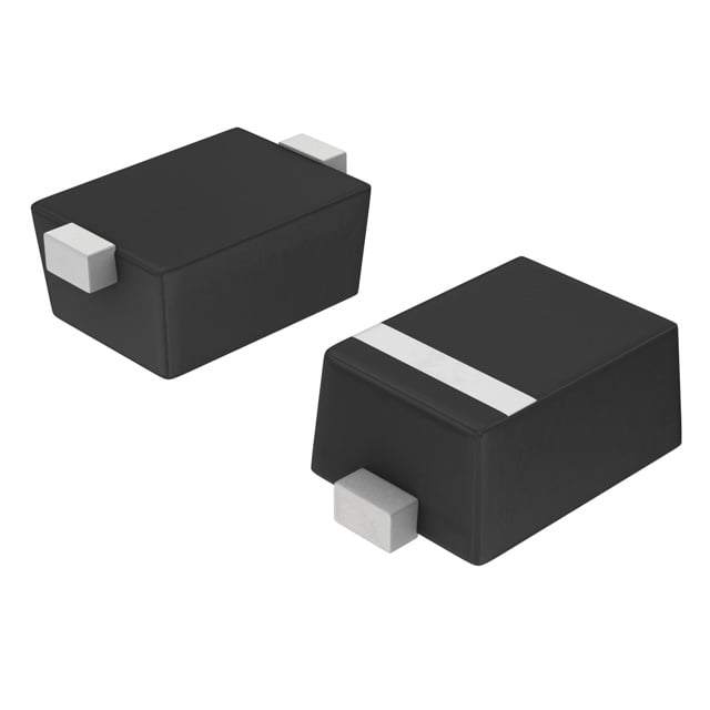
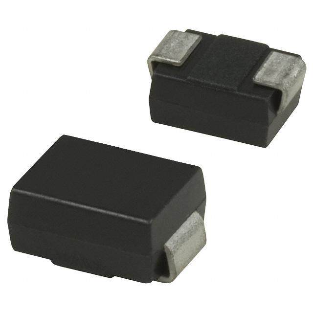
| 产品图片 |
|
| rohs | 符合RoHS无铅 / 符合限制有害物质指令(RoHS)规范要求 |
| 产品系列 | 二极管与整流器,肖特基二极管与整流器,ON Semiconductor NSR0240P2T5G- |
| 数据手册 | |
| 产品型号 | NSR0240P2T5G |
| PCN设计/规格 | |
| 不同If时的电压-正向(Vf) | 600mV @ 200mA |
| 不同 Vr、F时的电容 | 7pF @ 1V,1MHz |
| 不同 Vr时的电流-反向漏电流 | 5µA @ 40V |
| 二极管类型 | |
| 产品 | Schottky Diodes |
| 产品种类 | 肖特基二极管与整流器 |
| 供应商器件封装 | SOD-923 |
| 其它名称 | NSR0240P2T5GOSDKR |
| 包装 | Digi-Reel® |
| 反向恢复时间(trr) | - |
| 商标 | ON Semiconductor |
| 安装类型 | 表面贴装 |
| 安装风格 | SMD/SMT |
| 封装 | Reel |
| 封装/外壳 | SOD-923 |
| 封装/箱体 | SOD-923 |
| 峰值反向电压 | 40 V |
| 工作温度-结 | -55°C ~ 150°C |
| 工作温度范围 | - 55 C to + 150 C |
| 工厂包装数量 | 8000 |
| 技术 | Silicon |
| 最大反向漏泄电流 | 5 uA |
| 最大工作温度 | + 150 C |
| 最大浪涌电流 | 2 A |
| 最小工作温度 | - 55 C |
| 标准包装 | 1 |
| 正向电压下降 | 0.6 V |
| 正向连续电流 | 0.2 A |
| 热阻 | 520°C/W Ja |
| 电压-DC反向(Vr)(最大值) | 40V |
| 电流-平均整流(Io) | 200mA(DC) |
| 系列 | NSR0240P2 |
| 速度 | 小信号 =< 200mA(Io),任意速度 |
| 配置 | Single |


- 商务部:美国ITC正式对集成电路等产品启动337调查
- 曝三星4nm工艺存在良率问题 高通将骁龙8 Gen1或转产台积电
- 太阳诱电将投资9.5亿元在常州建新厂生产MLCC 预计2023年完工
- 英特尔发布欧洲新工厂建设计划 深化IDM 2.0 战略
- 台积电先进制程称霸业界 有大客户加持明年业绩稳了
- 达到5530亿美元!SIA预计今年全球半导体销售额将创下新高
- 英特尔拟将自动驾驶子公司Mobileye上市 估值或超500亿美元
- 三星加码芯片和SET,合并消费电子和移动部门,撤换高东真等 CEO
- 三星电子宣布重大人事变动 还合并消费电子和移动部门
- 海关总署:前11个月进口集成电路产品价值2.52万亿元 增长14.8%


.jpg)

PDF Datasheet 数据手册内容提取
NSR0240P2T5G Schottky Barrier Diode Schottky barrier diodes are optimized for very low forward voltage drop and low leakage current and are used in a wide range of dc−dc converter, clamping and protection applications in portable devices. NSR0240P2 in a SOD−923 miniature package enables designers to meet the challenging task of achieving higher efficiency and meeting www.onsemi.com reduced space requirements. Features • 40 V SCHOTTKY Very Low Forward Voltage Drop − 460 mV @ 100 mA • Low Reverse Current − 0.2 (cid:2)A @ 25 V VR BARRIER DIODE • 200 mA of Continuous Forward Current • Power Dissipation of 240 mW with Minimum Trace • Very High Switching Speed 1 2 • Low Capacitance − CT = 7 pF CATHODE ANODE • NSV Prefix for Automotive and Other Applications Requiring Unique Site and Control Change Requirements; AEC−Q101 MARKING Qualified and PPAP Capable • 2 DIAGRAM This is a Pb−Free Device 1 Typical Applications P M(cid:2) SOD−923 (cid:2) • LCD and Keypad Backlighting CASE 514AB 1 2 • Camera Photo Flash • Buck and Boost dc−dc Converters P = Specific Device Code • Reverse Voltage and Current Protection M = Month Code • (cid:2) = Pb−Free Package Clamping & Protection (Note: Microdot may be in either location) Markets • Mobile Handsets ORDERING INFORMATION • MP3 Players • Device Package Shipping† Digital Camera and Camcorders • Notebook PCs & PDAs NSR0240P2T5G SOD−923 8000 / Tape & Reel • (Pb−Free) GPS NSVR0240P2T5G SOD−923 8000 / Tape & Reel MAXIMUM RATINGS (Pb−Free) Rating Symbol Value Unit †For information on tape and reel specifications, Reverse Voltage VR 40 V including part orientation and tape sizes, please refer to our Tape and Reel Packaging Specifications Forward Current (DC) IF 200 mA Brochure, BRD8011/D. Non−Repetitive Peak Forward Surge Current IFSM 2.0 A ESD Rating: Human Body Model ESD Class 1C Machine Model Class A Stresses exceeding those listed in the Maximum Ratings table may damage the device. If any of these limits are exceeded, device functionality should not be assumed, damage may occur and reliability may be affected. © Semiconductor Components Industries, LLC, 2015 1 Publication Order Number: January, 2015 − Rev. 3 NSR0240P2/D
NSR0240P2T5G THERMAL CHARACTERISTICS Characteristic Symbol Min Typ Max Unit Thermal Resistance Junction−to−Ambient (Note 1) R(cid:3)JA 520 °C/W Total Power Dissipation @ TA = 25°C PD 240 mW Thermal Resistance Junction−to−Ambient (Note 2) R(cid:3)JA 175 °C/W Total Power Dissipation @ TA = 25°C PD 710 mW Junction and Storage Temperature Range TJ, Tstg −55 to +150 °C 1. Mounted onto a 4 in square FR−4 board 10 mm sq. 1 oz. Cu 0.06” thick single sided. Operating to steady state. 2. Mounted onto a 4 in square FR−4 board 1 in sq. 1 oz. Cu 0.06” thick single sided. Operating to steady state. ELECTRICAL CHARACTERISTICS (TA = 25°C unless otherwise noted) Characteristic Symbol Min Typ Max Unit Reverse Leakage IR (cid:2)A (VR = 25 V) 0.2 0.55 (VR = 40 V) 0.8 5.0 Forward Voltage (IF = 10 mA) VF 0.34 0.365 V (IF = 100 mA) 0.46 0.50 (IF = 200 mA) 0.54 0.60 Total Capacitance CT 7.0 pF (VR = 1.0 V, f = 1 MHz) 1000 1.0E−02 mA) 100 A)1.0E−03 150°C NT ( 125°C NT (1.0E−04 125°C 85°C E 10 E RR RR1.0E−05 75°C U 150°C U C 1 C1.0E−06 RD SE 25°C A R1.0E−07 W 0.1 E V OR RE1.0E−08 −40°C , FF0.01 I, r1.0E−09 I 85°C 25°C −40°C 0.001 1.0E−10 0 0.1 0.2 0.3 0.4 0.5 0.6 0 5 10 15 20 25 30 35 40 45 VF, FORWARD VOLTAGE (V) VR, REVERSE VOLTAGE (V) Figure 1. Forward Voltage Figure 2. Leakage Current 14 pF) 12 TA = 25°C E ( C 10 N A T CI 8 A P A 6 C L A T 4 O T C, T 2 0 0 5 10 15 20 25 30 35 40 45 VR, REVERSE VOLTAGE (V) Figure 3. Total Capacitance www.onsemi.com 2
NSR0240P2T5G PACKAGE DIMENSIONS SOD−923 CASE 514AB ISSUE C −X− D NOTES: 1. DIMENSIONING AND TOLERANCING PER ASME −Y− Y14.5M, 1994. 2. CONTROLLING DIMENSION: MILLIMETERS. E 3. MAXIMUM LEAD THICKNESS INCLUDES LEAD FINISH. MINIMUM LEAD THICKNESS IS THE 1 2 MINIMUM THICKNESS OF BASE MATERIAL. 2Xb 4. DIMENSIONS D AND E DO NOT INCLUDE MOLD FLASH, PROTRUSIONS, OR GATE BURRS. 0.08 X Y TOP VIEW MILLIMETERS INCHES DIM MIN NOM MAX MIN NOM MAX A A 0.34 0.37 0.40 0.013 0.015 0.016 b 0.15 0.20 0.25 0.006 0.008 0.010 c 0.07 0.12 0.17 0.003 0.005 0.007 D 0.75 0.80 0.85 0.030 0.031 0.033 E 0.55 0.60 0.65 0.022 0.024 0.026 HE 0.95 1.00 1.05 0.037 0.039 0.041 L 0.19 REF 0.007 REF c HE L2 0.05 0.10 0.15 0.002 0.004 0.006 SIDE VIEW SOLDERING FOOTPRINT* 2XL 1.20 2X 0.36 2X 0.25 2XL2 PACKAGE BOTTOM VIEW OUTLINE DIMENSIONS: MILLIMETERS See Application Note AND8455/D for more mounting details *For additional information on our Pb−Free strategy and soldering details, please download the ON Semiconductor Soldering and Mounting Techniques Reference Manual, SOLDERRM/D. ON Semiconductor and are registered trademarks of Semiconductor Components Industries, LLC (SCILLC). SCILLC owns the rights to a number of patents, trademarks, copyrights, trade secrets, and other intellectual property. A listing of SCILLC’s product/patent coverage may be accessed at www.onsemi.com/site/pdf/Patent−Marking.pdf. SCILLC reserves the right to make changes without further notice to any products herein. SCILLC makes no warranty, representation or guarantee regarding the suitability of its products for any particular purpose, nor does SCILLC assume any liability arising out of the application or use of any product or circuit, and specifically disclaims any and all liability, including without limitation special, consequential or incidental damages. “Typical” parameters which may be provided in SCILLC data sheets and/or specifications can and do vary in different applications and actual performance may vary over time. All operating parameters, including “Typicals” must be validated for each customer application by customer’s technical experts. SCILLC does not convey any license under its patent rights nor the rights of others. SCILLC products are not designed, intended, or authorized for use as components in systems intended for surgical implant into the body, or other applications intended to support or sustain life, or for any other application in which the failure of the SCILLC product could create a situation where personal injury or death may occur. Should Buyer purchase or use SCILLC products for any such unintended or unauthorized application, Buyer shall indemnify and hold SCILLC and its officers, employees, subsidiaries, affiliates, and distributors harmless against all claims, costs, damages, and expenses, and reasonable attorney fees arising out of, directly or indirectly, any claim of personal injury or death associated with such unintended or unauthorized use, even if such claim alleges that SCILLC was negligent regarding the design or manufacture of the part. SCILLC is an Equal Opportunity/Affirmative Action Employer. This literature is subject to all applicable copyright laws and is not for resale in any manner. PUBLICATION ORDERING INFORMATION LITERATURE FULFILLMENT: N. American Technical Support: 800−282−9855 Toll Free ON Semiconductor Website: www.onsemi.com Literature Distribution Center for ON Semiconductor USA/Canada P.O. Box 5163, Denver, Colorado 80217 USA Europe, Middle East and Africa Technical Support: Order Literature: http://www.onsemi.com/orderlit Phone: 303−675−2175 or 800−344−3860 Toll Free USA/Canada Phone: 421 33 790 2910 Fax: 303−675−2176 or 800−344−3867 Toll Free USA/Canada Japan Customer Focus Center For additional information, please contact your local Email: orderlit@onsemi.com Phone: 81−3−5817−1050 Sales Representative www.onsemi.com NSR0240P2/D 3
Mouser Electronics Authorized Distributor Click to View Pricing, Inventory, Delivery & Lifecycle Information: O N Semiconductor: NSR0240P2T5G