
 Datasheet下载
- 型号: NOIV1SN1300A-QDC
- 制造商: ON Semiconductor
- 库位|库存: xxxx|xxxx
- 要求:
| 数量阶梯 | 香港交货 | 国内含税 |
| +xxxx | $xxxx | ¥xxxx |
查看当月历史价格
查看今年历史价格
NOIV1SN1300A-QDC产品简介:
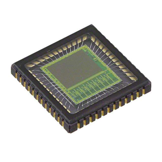
ICGOO电子元器件商城为您提供NOIV1SN1300A-QDC由ON Semiconductor设计生产,在icgoo商城现货销售,并且可以通过原厂、代理商等渠道进行代购。 NOIV1SN1300A-QDC价格参考。ON SemiconductorNOIV1SN1300A-QDC封装/规格:图像传感器,相机, CMOS Image Sensor 1280H x 1024V 4.8µm x 4.8µm 48-LCC (14.22x14.22)。您可以下载NOIV1SN1300A-QDC参考资料、Datasheet数据手册功能说明书,资料中有NOIV1SN1300A-QDC 详细功能的应用电路图电压和使用方法及教程。
| 参数 | 数值 |
| 产品目录 | |
| 描述 | IC IMAGE SENSOR 1.3MP 48LCC |
| 产品分类 | |
| 品牌 | ON Semiconductor |
| 数据手册 | |
| 产品图片 |
|
| 产品型号 | NOIV1SN1300A-QDC |
| rohs | 无铅 / 符合限制有害物质指令(RoHS)规范要求 |
| 产品系列 | - |
| 供应商器件封装 | 48-LCC(14.22x14.22) |
| 像素尺寸 | 4.8µm x 4.8µm |
| 其它名称 | NOIV1SN1300A-QDC-ND |
| 包装 | 托盘 |
| 备注 | - |
| 封装/外壳 | 48-LCC |
| 有源像素阵列 | 1280H x 1024V |
| 标准包装 | 64 |
| 每秒帧数 | 150 |
| 电压-电源 | 1.8V, 3.3V |
| 类型 | CMOS 成像 |


- 商务部:美国ITC正式对集成电路等产品启动337调查
- 曝三星4nm工艺存在良率问题 高通将骁龙8 Gen1或转产台积电
- 太阳诱电将投资9.5亿元在常州建新厂生产MLCC 预计2023年完工
- 英特尔发布欧洲新工厂建设计划 深化IDM 2.0 战略
- 台积电先进制程称霸业界 有大客户加持明年业绩稳了
- 达到5530亿美元!SIA预计今年全球半导体销售额将创下新高
- 英特尔拟将自动驾驶子公司Mobileye上市 估值或超500亿美元
- 三星加码芯片和SET,合并消费电子和移动部门,撤换高东真等 CEO
- 三星电子宣布重大人事变动 还合并消费电子和移动部门
- 海关总署:前11个月进口集成电路产品价值2.52万亿元 增长14.8%


PDF Datasheet 数据手册内容提取
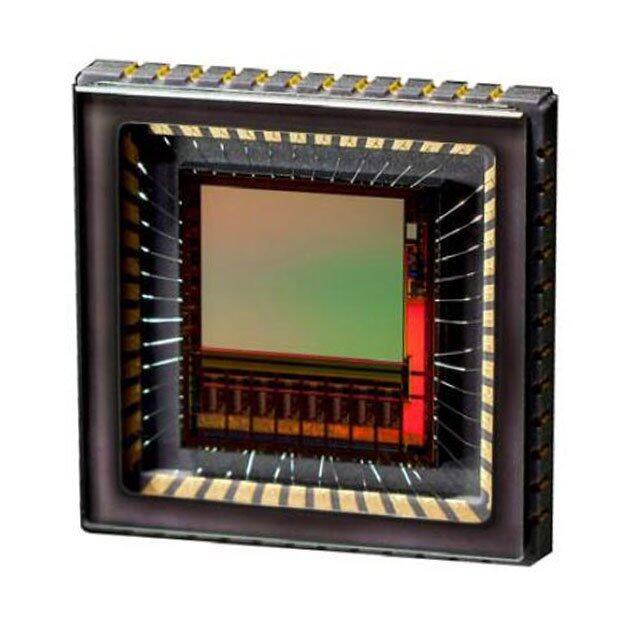
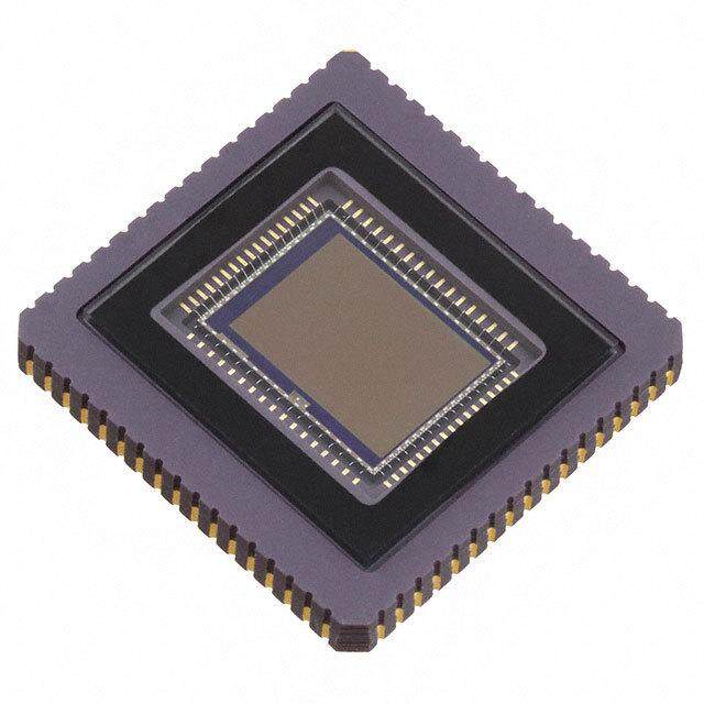
NOIV1SN1300A, NOIV2SN1300A VITA 1300 1.3 Megapixel 150 FPS Global Shutter CMOS Image Sensor www.onsemi.com Features • SXGA: 1280 x 1024 Active Pixels • 4.8 (cid:2)m x 4.8 (cid:2)m Pixel Size • 1/2 inch Optical Format • Monochrome (SN) or Color (SE) • 150 Frames per Second (fps) at Full Resolution (LVDS) • 37 Frames per Second (fps) at Full Resolution (CMOS) • On-chip 10-bit Analog-to-Digital Converter (ADC) • 8-bit or 10-bit Output Mode • Four LVDS Serial Outputs or Parallel CMOS Output • Random Programmable Region of Interest (ROI) Readout • Pipelined and Triggered Global Shutter, Rolling Shutter • On-chip Fixed Pattern Noise (FPN) Correction • Serial Peripheral Interface (SPI) • Automatic Exposure Control (AEC) • Phase Locked Loop (PLL) Figure 1. VITA 1300 Photograph • High Dynamic Range (HDR) • Dual Power Supply (3.3 V and 1.8 V) • −40°C to +85°C Operational Temperature Range Applications • • Machine Vision 48-pin LCC and Bare Die • • Motion Monitoring 475 mW Power Dissipation (LVDS) • • Security 290 mW Power Dissipation (CMOS) • • Barcode Scanning (2D) These Devices are Pb−Free and are RoHS Compliant Description The VITA 1300 is a 1/2 inch Super-eXtended Graphics Array (SXGA) CMOS image sensor with a pixel array of 1280 by 1024. The high sensitivity 4.8 (cid:2)m x 4.8 (cid:2)m pixels support pipelined and triggered global shutter readout modes and can also be operated in a low noise rolling shutter mode. In rolling shutter mode, the sensor supports correlated double sampling readout, reducing noise and increasing the dynamic range. The sensor has on-chip programmable gain amplifiers and 10-bit A/D converters. The integration time and gain parameters can be reconfigured without any visible image artifact. Optionally the on-chip automatic exposure control loop (AEC) controls these parameters dynamically. The image’s black level is either calibrated automatically or can be adjusted by adding a user programmable offset. A high level of programmability using a four wire serial peripheral interface enables the user to read out specific regions of interest. Up to 8 regions can be programmed, achieving even higher frame rates. The image data interface of the V1-SN/SE part consists of four LVDS lanes, facilitating frame rates up to 150 frames per second. Each channel runs at 620 Mbps. A separate synchronization channel containing payload information is provided to facilitate the image reconstruction at the receive end. The V2-SN/SE part provides a parallel CMOS output interface at reduced frame rate. The VITA 1300 is packaged in a 48-pin LCC package and is available in a monochrome and color version. Contact your local ON Semiconductor office for more information. © Semiconductor Components Industries, LLC, 2014 1 Publication Order Number: December, 2016 − Rev. 10 NOIV1SN1300A/D
NOIV1SN1300A, NOIV2SN1300A ORDERING INFORMATION Part Number Mono/Color Package NOIV1SN1300A-QDC LVDS Interface mono 48−pin LCC NOIV1SE1300A-QDC LVDS Interface color NOIV2SN1300A-QDC CMOS Interface mono NOIV2SE1300A-QDC CMOS Interface color NOIV1SN1300A-XXC Die sales, mono Die Sales The V1-SN/SE base part is used to reference the mono and part is used to reference the mono and color versions of the color versions of the LVDS interface; the V2-SN/SE base CMOS interface. ORDERING CODE DEFINITION PACKAGE MARK Following is the mark on the bottom side of the package with Pin 1 to the left center Line 1: NOI xxxx 1300A where xxxx denotes LVDS (V1) / CMOS (V2), mono micro lens (SN) /color micro lens (SE) option Line 2: -QDC Line 3: AWLYYWW www.onsemi.com 2
NOIV1SN1300A, NOIV2SN1300A CONTENTS Features..................................... 1 Sensor Operation ............................. 15 Applications ................................. 1 Image Sensor Timing and Readout .............. 30 Description .................................. 1 Additional Features ........................... 33 Ordering Information ......................... 2 Data Output Format .......................... 41 Ordering Code Definition ...................... 2 Register Map ................................ 50 Package Mark................................ 2 Package Information .......................... 66 Contents .................................... 3 Specifications and Useful References ............. 72 Specifications ................................ 4 Silicon Errata ................................ 73 Overview .................................... 8 Acronyms ................................... 74 Operating Modes ............................. 12 Glossary .................................... 75 www.onsemi.com 3
NOIV1SN1300A, NOIV2SN1300A SPECIFICATIONS Key Specifications Table 1. GENERAL SPECIFICATIONS Table 2. ELECTRO−OPTICAL SPECIFICATIONS Parameter Specification Parameter Specification Pixel type Global shutter pixel architecture Active pixels 1280 (H) x 1024 (V) Shutter type Pipelined and triggered global shutter, Pixel size 4.8 (cid:2)m x 4.8 (cid:2)m rolling shutter Optical format 1/2 inch Frame rate V1-SN/SE: 150 fps Conversion gain 0.072 LSB10/e- at full resolution V2-SN/SE: 37 fps 90 (cid:2)V/e- Master clock V1-SN/SE: Dark noise 2.2 LSB10, 30e- in global shutter 62 MHz when PLL is used, 0.9 LSB10, 14e-in rolling shutter 310 MHz (10-bit) / 248 MHz (8-bit) when PLL is not used Responsivity at 550 nm 24 LSB10 /nJ/cm2, 4.6 V/lux.s V2-SN/SE: 62 MHz Parasitic Light <1/450 Windowing 8 Randomly programmable windows. Sensitivity (PLS) Normal, sub-sampled and binned read- out modes Full well charge 13700 e- ADC resolution (1) 10-bit, 8-bit Quantum efficiency 53% at 550 nm LVDS outputs V1-SN/SE: 4 data + sync + clock Pixel FPN rolling shutter: 0.5 LSB10 global shutter: 1.0 LSB10 CMOS outputs V2-SN/SE: 10-bit parallel output, frame_valid, line_valid, clock PRNU < 2% of signal Data rate V1-SN/SE: MTF 60% @ 630 nm - X-dir & Y-dir 4 x 620 Mbps (10-bit) / PSNL @ 25°C 100 LSB10/s, 1360 e-/s 4 x 496 Mbps (8-bit) Dark signal @ 25°C 4.5 e-/s, 0.33 LSB10/s V2-SN/SE: 62 MHz Dynamic range 60 dB in rolling shutter mode Power dissipation 475 mW for V1-SN/SE in 10-bit mode 53 dB in global shutter mode 290 mW for V2-SN/SE Signal to Noise Ratio 41 dB Package type 48-pin LCC, bare die (SNR max) Table 3. RECOMMENDED OPERATING RATINGS (Note 2) Symbol Description Min Max Units TJ Operating temperature range −40 85 °C Table 4. ABSOLUTE MAXIMUM RATINGS (Notes 3 and 4) Symbol Parameter Min Max Units ABS (1.8 V supply group) ABS rating for 1.8 V supply group –0.5 2.2 V ABS (3.3 V supply group) ABS rating for 3.3 V supply group –0.5 4.3 V TS ABS storage temperature range −40 +150 °C ABS storage humidity range at 85°C 85 %RH Electrostatic discharge (ESD) Human Body Model (HBM): JS−001−2010 2000 V Charged Device Model (CDM): JESD22−C101 500 LU Latch-up: JESD−78 140 mA Stresses exceeding Maximum Ratings may damage the device. Maximum Ratings are stress ratings only. Functional operation above the Recommended Operating Conditions is not implied. Extended exposure to stresses above the Recommended Operating Conditions may affect device reliability. 1. The ADC is 11−bit, down−scaled to 10−bit. The VITA 1300 uses a larger word−length internally to provide 10−bit on the output. 2. Operating ratings are conditions in which operation of the device is intended to be functional. 3. ON Semiconductor recommends that customers become familiar with, and follow the procedures in JEDEC Standard JESD625−A. Refer to Application Note AN52561. Long term exposure toward the maximum storage temperature will accelerate color filter degradation. 4. Caution needs to be taken to avoid dried stains on the underside of the glass due to condensation. The glass lid glue is permeable and can absorb moisture if the sensor is placed in a high % RH environment. www.onsemi.com 4
NOIV1SN1300A, NOIV2SN1300A Table 5. ELECTRICAL SPECIFICATIONS Boldface limits apply for TJ = TMIN to TMAX, all other limits TJ = +30°C. (Notes 5, 6 and 7) Parameter Description Min Typ Max Units Power Supply Parameters - V1-SN/SE LVDS vdd_33 Supply voltage, 3.3 V 3.0 3.3 3.6 V Idd_33 Current consumption 3.3 V supply 90 110 130 mA vdd_18 Supply voltage, 1.8 V 1.6 1.8 2.0 V Idd_18 Current consumption 1.8 V supply 45 60 75 mA vdd_pix Supply voltage, pixel 3.0 3.3 3.6 V Idd_pix Current consumption pixel supply 0.8 1.8 2.5 mA Ptot Total power consumption at vdd_33 = 3.3 V, vdd_18 = 1.8 V 375 475 575 mW Pstby_lp Power consumption in low power standby mode. See Silicon Errata 50 mW on page 66 Popt Power consumption at lower pixel rates Configurable Power Supply Parameters - V2-SN/SE CMOS vdd_33 Supply voltage, 3.3 V 3.0 3.3 3.6 V Idd_33 Current consumption 3.3 V supply 70 90 110 mA vdd_18 Supply voltage, 1.8 V 1.6 1.8 2.0 V Idd_18 Current consumption 1.8 V supply 4 7 10 mA vdd_pix Supply voltage, pixel 3.0 3.3 3.6 V Idd_pix Current consumption pixel supply 0.5 1 mA Ptot Total power consumption 220 290 360 mW Pstby_lp Power consumption in low power standby mode. See Silicon Errata 50 mW on page 66 Popt Power consumption at lower pixel rates Configurable I/O - V2-SN/SE CMOS (JEDEC- JESD8C-01): Conforming to standard/additional specifications and deviations listed fpardata Data rate on parallel channels (10-bit) 62 Mbps Cout Output load (only capacitive load) 10 pF tr Rise time (10% to 90% of input signal) 2.5 4.5 6.5 ns tf Fall time (10% to 90% of input signal) 2 3.5 5 ns I/O - V1-SN/SE LVDS (EIA/TIA-644): Conforming to standard/additional specifications and deviations listed fserdata Data rate on data channels 620 Mbps DDR signaling - 4 data channels, 1 synchronization channel; fserclock Clock rate of output clock 310 MHz Clock output for mesochronous signaling Vicm LVDS input common mode level 0.3 1.25 2.2 V Tccsk Channel to channel skew (Training pattern allows per channel skew 50 ps correction) V1-SN/SE LVDS Electrical/Interface fin Input clock rate when PLL used 62 MHz fin Input clock when LVDS input used 310 MHz tidc Input clock duty cycle when PLL used 40 50 60 % tj Input clock jitter 20 ps fspi SPI clock rate when PLL used at fin = 62 MHz 10 MHz V2-SN/SE CMOS Electrical/Interface fin Input clock rate 62 MHz www.onsemi.com 5
NOIV1SN1300A, NOIV2SN1300A Table 5. ELECTRICAL SPECIFICATIONS Boldface limits apply for TJ = TMIN to TMAX, all other limits TJ = +30°C. (Notes 5, 6 and 7) Parameter Description Min Typ Max Units tj Input clock jitter 20 ps fspi SPI clock rate at fin = 62 MHz 2.5 MHz Frame Specifications (V1-SN/SE-LVDS - Global Shutter) fps Frame rate at full resolution 150 fps fps_roi1 Xres x Yres = 1024 x 1024 180 fps fps_roi2 Xres x Yres = 640 x 480 540 fps fps_roi3 Xres x Yres = 512 x 512 590 fps fps_roi4 Xres x Yres = 256 x 256 1650 fps FOT Frame Overhead Time 45 (cid:2)s ROT Row Overhead Time 1.1 (cid:2)s fpix Pixel rate (4 channels at 62 Mpix/s) 248 Mpix/s Frame Specifications (V2-SN/SE CMOS - Global Shutter) fps Frame rate at full resolution 37 fps 5. All parameters are characterized for DC conditions after thermal equilibrium is established. 6. This device contains circuitry to protect the inputs against damage due to high static voltages or electric fields. However, it is recommended that normal precautions be taken to avoid application of any voltages higher than the maximum rated voltages to this high impedance circuit. 7. Minimum and maximum limits are guaranteed through test and design. For recommendations on power supply management guidelines, refer to application note AN65463: VITA 1300 HSMC Cyclone Reference Board Design Recommenda- tions. Y Color Filter Array The V1SE and V2SE sensors are processed with a Bayer RGB color pattern as shown in Figure 2. Pixel (0,0) has a red filter situated to the bottom left. X pixel (0;0) Figure 2. Color Filter Array for the Pixel Array www.onsemi.com 6
NOIV1SN1300A, NOIV2SN1300A Spectral Response Curve Figure 3. Spectral Response Curve for Mono and Color Note that green pixels on a Green−Red (Green 1) and Green−Blue (Green 2) row have similar responsivity to wavelength trend as is depicted by the legend “Green”. www.onsemi.com 7
NOIV1SN1300A, NOIV2SN1300A OVERVIEW Figure 4 and Figure 5 give an overview of the major are fed into the data formatting block. This block adds functional blocks of the V1-SN/SE and V2-SN/SE sensor synchronization information to the data stream based on the respectively. The system clock is received by the CMOS frame timing. For the V1-SN/SE version, the data then goes clock input. A PLL generates the intenal, high speed, clocks, to the low voltage serial (LVDS) interface block which sends which are distributed to the other blocks. Optionally, the the data out through the I/O ring. The V2-SN/SE sensor does V1-SN/SE can also accept a high speed LVDS clock, in not have an LVDS interface but sends out the data through which case the PLL will be disabled. a 10-bit parallel interface. The sequencer defines the sensor timing and controls the On-chip programmability is achieved through the Serial image core. The sequencer is started either autonomously Peripheral Interface (SPI). See the Register Map on page50 (master mode) or on assertion of an external trigger (slave for register details. mode). The image core contains all pixels and readout A bias block generates bias currents and voltages for all circuits. The column structure selects pixels for readout and analog blocks on the chip. By controlling the bias current, performs correlated double sampling (CDS) or double the speed-versus-power of each block can be tuned. All sampling (DS). The data comes out sequentially and is fed biasing programmability is contained in the bias block. into the analog front end (AFE) block. The programmable The sensor can automatically control exposure and gain gain amplifier (PGA) of the AFE adds the offset and gain. by enabling the automatic exposure control block (AEC). The output is a fully differential analog signal that goes to the This block regulates the integration time along with the ADC, where the analog signal is converted to a 10-bit data analog and digital gains to reach the desired intensity. stream. Depending on the operating mode, eight or ten bits www.onsemi.com 8
NOIV1SN1300A, NOIV2SN1300A Block Diagram Image Core Image Core Bias er d(cid:2) o c(cid:2) e D Pixel Array w (1280x1024) o R Column Structure Automatic Exposure 8 analog channels Control (AEC) Analog Front End (AFE) 8 x 10 bit Control & digital channels Registers Data Formatting Clock Distribution 4 x 10 bit digital channels Serializers & LVDS Interface PLL LVDS Receiver 4 LVDS Channels 1 LVDS Sync Channel 1 LVDS Clock Channel s CMOInSp uCtlock LVDInSp Cutlock nterface Tr(cid:2)i(cid:2)gger(cid:2) Re(cid:2)set LVDS Interface PI I al(cid:2) S n er(cid:2) xt(cid:2) E Figure 4. Block Diagram − V1−SN/SE www.onsemi.com 9
NOIV1SN1300A, NOIV2SN1300A Block Diagram Image Core Image Core Bias er d(cid:2) o c(cid:2) e D Pixel Array w (1280x1024) o R Column Structure Automatic Exposure 8 analog channels Control (AEC) Analog Front End (AFE) 8 x 10 bit Control & digital channels Registers Data Formatting 4 x 10 bit Clock digital channels Distribution Output MUX PLL 10 bit Parallel Data Frame Valid Indication CMOInSp uCtlock nterface Tr(cid:2)i(cid:2)gger(cid:2)s Re(cid:2)set CMOS Interface Line Valid Indication PI I al(cid:2) S n er(cid:2) xt(cid:2) E Figure 5. Block Diagram − V2−SN/SE Image Core sequencer and can access the pixel array in global and rolling The image core consists of: shutter modes. • Pixel Array The pixel biasing block guarantees that the data on a pixel • is transferred properly to the column multiplexer when the Address Decoders and Row Drivers • row drivers select a pixel line for readout. Pixel Biasing The pixel array contains 1280 (H) x 1024 (V) readable Phase Locked Loop pixels with a pixel pitch of 4.8 (cid:2)m. Four dummy pixel rows The PLL accepts a (low speed) clock and generates the and columns are placed at every side of the pixel array to required high speed clock. Optionally this PLL can be eliminate possible edge effects. The sensor uses a 5T pixel bypassed. Typical input clock frequency is 62 MHz. architecture, which makes it possible to read out the pixel array in global shutter mode with double sampling (DS), or LVDS Clock Receiver The LVDS clock receiver receives an LVDS clock signal in rolling shutter mode with correlated double sampling and distributes the required clocks to the sensor. (CDS). Typical input clock frequency is 310 MHz in 10-bit mode The function of the row drivers is to access the image array and 248 MHz in 8-bit mode. The clock input needs to be line by line, or all lines together, to reset or read the pixel terminated with a 100 (cid:3) resistor. data. The row drivers are controlled by the on-chip www.onsemi.com 10
NOIV1SN1300A, NOIV2SN1300A Column Multiplexer Serializer and LVDS Interface (V1−SN/SE only) All pixels of one image row are stored in the column The serializer and LVDS interface block receives the sample-and-hold (S/H) stages. These stages store both the formatted (10-bit or 8-bit) data from the data formatting reset and integrated signal levels. block. This data is serialized and transmitted by the LVDS The data stored in the column S/H stages is read out output driver. through 8 parallel differential outputs operating at a In 10-bit mode, the maximum output data rate is 620 Mbps frequency of 31 MHz. per channel. In 8-bit mode, the maximum output data rate is At this stage, the reset signal and integrated signal values 496 Mbps per channel. are transferred into an FPN-corrected differential signal. In addition to the LVDS data outputs, two extra LVDS The column multiplexer also supports read-1-skip-1 and outputs are available. One of these outputs carries the output read-2-skip-2 mode. Enabling this mode can speed up the clock, which is skew aligned to the output data channels. The frame rate, with a decrease in resolution. second LVDS output contains frame format synchronization codes to serve system-level image reconstruction. Bias Generator The bias generator generates all required reference Output MUX (V2−SN/SE only) voltages and bias currents that the on-chip blocks use. An The output MUX multiplexes the four data channels to external resistor of 47 k(cid:3), connected between pin one channel and transmits the data words using a 10-bit IBIAS_MASTER and gnd_33, is required for the bias parallel CMOS interface. generator to operate properly. Frame synchronization information is communicated by means of frame and line valid strobes. Analog Front End The AFE contains 8 channels, each containing a PGA and Sequencer a 10-bit ADC. The sequencer: • For each of the 8 channels, a pipelined 10-bit ADC is used Controls the image core. Starts and stops integration in to convert the analog image data into a digital signal, which rolling and global shutter modes and control pixel is delivered to the data formatting block. A black calibration readout. loop is implemented to ensure that the black level is mapped • Operates the sensor in master or slave mode. to match the correct ADC input level. • Applies the window settings. Organizes readouts so that Data Formatting only the configured windows are read. • The data block receives data from two ADCs and Controls the column multiplexer and analog core. multiplexes this data to one data stream. A cyclic Applies gain settings and subsampling modes at the redundancy check (CRC) code is calculated on the passing correct time, without corrupting image data. data. • Starts up the sensor correctly when leaving standby A frame synchronization data block is foreseen to transmit mode. synchronization codes such as frame start, line start, frame end, and line end indications. Automatic Exposure Control The data block calculates a CRC once per line for every The AEC block implements a control system to modulate channel. This CRC code can be used for error detection at the the exposure of an image. Both integration time and gains receiving end. are controlled by this block to target a predefined illumination level. www.onsemi.com 11
NOIV1SN1300A, NOIV2SN1300A OPERATING MODES The VITA 1300 sensor is able to operate in the following shutter modes: • Global Shutter Mode ♦ Pipelined Global Shutter - Master - Slave ♦ Triggered Global Shutter - Master - Slave • Rolling Shutter Mode Global Shutter Mode In the global shutter mode, light integration takes place on all pixels in parallel, although subsequent readout is sequential. Figure 6 shows the integration and readout sequence for the synchronous shutter. All pixels are light Figure 6. Global Shutter Operation sensitive at the same period of time. The whole pixel core is reset simultaneously and after the integration time all pixel Pipelined Global Shutter values are sampled together on the storage node inside each In pipelined global shutter mode, the integration and pixel. The pixel core is read out line by line after integration. readout are done in parallel. Images are continuously read Note that the integration and readout can occur in parallel or and integration of frame N is ongoing during readout of the sequentially. previous frame N-1. The readout of every frame starts with a Frame Overhead Time (FOT), during which the analog value on the pixel diode is transferred to the pixel memory element. After the FOT, the sensor is read out line per line and the readout of each line is preceded by the Row Overhead Time (ROT). Figure 7 shows the exposure and readout time line in pipelined global shutter mode. • Master In this operation mode, the integration time is set through the register interface and the sensor integrates and reads out the images autonomously. The sensor acquires images without any user interaction. Integration Tim(cid:2)e Reset Reset Exposure Time N FOT Exposure Time N+1 FOT Handling N N+1 Readout FOT Readout Fram(cid:2)e N(cid:2)-1 FOT R(cid:2)eadout Fram(cid:2)e N FOT Handling ÉÉÉÉÉÉÉÉÉÉÉÉÉÉÉÉÉÉÉÉÉÉÉÉÉÉÉÉÉÉÉÉÉÉÉÉÉÉÉÉÉÉÉÉ ÉÉÉÉÉÉÉÉÉÉÉÉÉÉÉÉÉÉÉÉÉÉÉÉÉÉÉÉÉÉÉÉÉÉÉÉÉÉÉÉÉÉÉÉ ROT Line Readout Figure 7. Integration and Readout for Pipelined Shutter • Slave and integration starts. The integration continues until the The slave mode adds more manual control to the sensor. external pin is de-asserted by the system. Now, the image is The exposure time registers are ignored in this mode and the sampled and the readout is started. Figure 8 shows the integration time is controlled by an external pin. As soon as relation between the external trigger signal and the the control pin is asserted, the pixel array goes out of reset exposure/readout timing. www.onsemi.com 12
NOIV1SN1300A, NOIV2SN1300A External Trigger Integration Time Reset Reset Handling N Exposure Time N FOT N+1 Exposure Time N+1 FOT Readout Handling FOT Readout N−1 FOT Readout N FOT ÉÉÉÉÉÉÉÉÉÉÉÉÉÉÉÉÉÉÉÉÉÉÉÉÉÉÉÉÉÉÉÉÉÉÉÉÉÉÉÉÉÉÉÉ ÉÉÉÉÉÉÉÉÉÉÉÉÉÉÉÉÉÉÉÉÉÉÉÉÉÉÉÉÉÉÉÉÉÉÉÉÉÉÉÉÉÉÉÉ ROT Line Readout Figure 8. Pipelined Shutter Operated in Slave Mode Triggered Global Shutter The triggered global mode is also controlled in a master In this mode, manual intervention is required to control or slave mode fashion. both the integration time and the start of readout. After the • Master integration time, indicated by a user controlled pin, the In this mode, a rising edge on the synchronization pin is image core is read out. After this sequence, the sensor goes used to trigger the start of integration and readout. The to an idle mode until a new user action is detected. integration time is defined by a register setting. The sensor The three main differences with the pipelined global autonomously integrates during this predefined time, after shutter mode are which the FOT starts and the image array is readout • Upon user action, one single image is read. sequentially. A falling edge on the synchronization pin does • Integration and readout are done sequentially. However, not have any impact on the readout or integration and the user can control the sensor in such a way that two subsequent frames are started again for each rising edge. consecutive batches are overlapping, that is, having Figure 9 shows the relation between the external trigger concurrent integration and readout. signal and the exposure/readout timing. • If a rising edge is applied on the external trigger before the Integration and readout is under user control through an exposure time and FOT of the previous frame is complete, external pin. it is ignored by the sensor. This mode requires manual intervention for every frame. The pixel array is kept in reset state until requested. No effect on falling edge External Trigger Integration Tim(cid:2)e Reset Reset Exposure Tim(cid:2)e N FOT Exposure Tim(cid:2)e N(cid:2)+1 FOT Handling N N+1 Register Controlled Readout FOT Readout N(cid:2)-1 FOT Readout N FOT Handling ÉÉÉÉÉÉÉÉÉÉÉÉÉÉÉÉÉÉÉÉÉÉÉÉÉÉÉÉÉÉÉÉÉÉÉÉÉÉÉÉÉÉÉÉ ÉÉÉÉÉÉÉÉÉÉÉÉÉÉÉÉÉÉÉÉÉÉÉÉÉÉÉÉÉÉÉÉÉÉÉÉÉÉÉÉÉÉÉÉ ROT Line Readout Figure 9. Triggered Shutter Operated in Master Mode • Slave FOT starts. The analog value on the pixel diode is Integration time control is identical to the pipelined transferred to the pixel memory element and the image shutter slave mode. An external synchronization pin readout can start. A request for a new frame is started when controls the start of integration. When it is de-asserted, the the synchronization pin is asserted again. www.onsemi.com 13
NOIV1SN1300A, NOIV2SN1300A Rolling Shutter Mode Figure 10 schematically indicates the relative shift of the Another shutter mode supported by the sensor is the integration times of different lines during the rolling shutter rolling shutter mode. The shutter mechanism is an electronic operation. Each row is read and reset in a sequential way. rolling shutter and the sensor operates in a streaming mode Each row in a particular frame is integrated for the same similar to a video. This mechanism is controlled by the time, but all lines in a frame ‘see’ a different stare time. As on-chip sequencer logic. There are two Y pointers. One a consequence, fast horizontal moving objects in the field of points to the row that is to be reset for rolling shutter view give rise to motion artifacts in the image; this is an operation, the other points to the row to be read out. unavoidable property of a rolling shutter. Functionally, a row is reset first and selected for read out In rolling shutter mode, the pixel Fixed Pattern Noise sometime later. The time elapsed between these two (FPN) is corrected on-chip by using the CDS technique. operations is the exposure time. After light integration on all pixels in a row is complete, the storage node in the pixel is reset. Afterwards the integrated signal is transferred to that pixel storage node. The difference between the reset level and integrated signal is the FPN corrected signal. The advantage of this technique, compared to the DS technique used in the global shutter modes, is that the reset noise of the pixel storage node is cancelled. This results in a lower temporal noise level. Figure 10. Rolling Shutter Operation www.onsemi.com 14
NOIV1SN1300A, NOIV2SN1300A SENSOR OPERATION Flowchart Low Power Standby Figure 11 shows the sensor operation flowchart. The In low power standby state, all power supplies are on, but sensor can be in six different ‘states’. Every state is indicated internally every block is disabled. No internal clock is with the oval circle. These states are: running (PLL / LVDS clock receiver is disabled). • Power off All register settings are unchanged. • Low power standby Only a subset of the SPI registers is active for read/write • in order to be able to configure clock settings and leave the Standby (1) • low power standby state. The only SPI registers that should Standby (2) be touched are the ones required for the ‘Enable Clock • Idle Management’ action described in Enable Clock • Running Management − Part 1 on page 17 These states are ordered by power dissipation. In Standby (1) ‘power-off’ state, the power dissipation is minimal; in In standby state, the PLL/LVDS clock receiver is running, ‘running’ state the power dissipation is maximal. but the derived logic clock signal is not enabled. On the other hand, the lower the power consumption, the Standby (2) more actions (and time) are required to put the sensor in In standby state, the derived logic clock signal is running. ‘running’ state and grab images. All SPI registers are active, meaning that all SPI registers This flowchart allows the trade-off between power saving can be accessed for read or write operations. All other blocks and enabling time of the sensor. are disabled. Next to the six ‘states’ a set of ‘user actions’, indicated by arrows, are included in the flowchart. These user actions Idle make it possible to move from one state to another. In the idle state, all internal blocks are enabled, except the sequencer block. The sensor is ready to start grabbing Sensor States images as soon as the sequencer block is enabled. Power Off Running In this state, the sensor is inactive. All power supplies are In running state, the sensor is enabled and grabbing down and the power dissipation is zero. images. The sensor can be operated in different rolling/global master/slave modes. www.onsemi.com 15
NOIV1SN1300A, NOIV2SN1300A Power Off Power Down Sequence Power Up Sequence Low-Power Standby Disable Clock Management Enable Clock Management - Part 1 Part 1 Poll Lock Indication Standby (1) (only when PLL is enabled) 2 art(cid:2) et) Ps - Re nt(cid:2) d meHar Enable Clock Management - Part 2 ageer (First Pass after Hard Reset) anaft Disable Clock Management Ms Part 2 k as Intermediate Standby cP e CloFirst n Pi(cid:2)n Enabl(Not RUepqlouairded Register eset(cid:2)_ r of(cid:2) n o Sensor (re-)configuration ert(cid:2)i Standby (2) s (optional) s A Soft Power-Down Soft Power-Up Sensor (re-)configuration Idle (optional) Enable Sequencer Disable Sequencer Sensor (re-)configuration Running (optional) Figure 11. Sensor Operation Flowchart www.onsemi.com 16
NOIV1SN1300A, NOIV2SN1300A User Actions: Power Up Functional Mode Sequences Enable Clock Management − Part 1 Power Up Sequence The ‘Enable Clock Management’ action configures the Figure 12 shows the power up sequence of the sensor. The clock management blocks and activates the clock generation figure indicates that the first supply to ramp-up is the vdd_18 and distribution circuits in a pre-defined way. First, a set of supply, followed by vdd_33 and vdd_pix respectively. It is clock settings must be uploaded through the SPI register. important to comply with the described sequence. Any other These settings are dependent on the desired operation mode supply ramping sequence may lead to high current peaks of the sensor. and, as consequence, a failure of the sensor power up. Table 6 shows the SPI uploads to be executed to configure The clock input should start running when all supplies are the sensor for V1-SN/SE 8-bit serial, V1-SN/SE 10-bit stabilized. When the clock frequency is stable, the reset_n serial, or V2-SN/SE 10-bit parallel mode, with and without signal can be de-asserted. After a wait period of 10 (cid:2)s, the the PLL. power up sequence is finished and the first SPI upload can In the serial modes, if the PLL is not used, the LVDS clock be initiated. input must be running. In the V2-SN/SE10-bit parallel mode, the PLL is NOTE: The ‘clock input’ can be the CMOS PLL clock bypassed. The clk_pll clock is used as sensor clock. input (clk_pll), or the LVDS clock input It is important to follow the upload sequence listed in (lvds_clock_inn/p) in case the PLL is bypassed. Table 6. Use of Phase Locked Loop clock input If PLL is used, the PLL is started after the upload of the reset_n SPI registers. The PLL requires (dependent on the settings) some time to generate a stable output clock. A lock detect vdd_18 circuit detects if the clock is stable. When complete, this is flagged in a status register. vdd_33 NOTE: The lock detect status must not be checked for the V2-SN/SE sensor. vdd_pix Check this flag by reading the SPI register. When the flag is set, the ‘Enable Clock Management- Part 2’ action can be SPI Upload continued. When PLL is not used, this step can be bypassed as shown in Figure 11 on page 16. > 10us > 10us > 10us > 10us > 10us Figure 12. Power Up Sequence Table 6. ENABLE CLOCK MANAGEMENT REGISTER UPLOAD − PART 1 Upload # Address Data Description V1-SN/SE 8-bit mode with PLL 1 2 0x0000 Monochrome sensor 0x0001 Color sensor 2 32 0x200C Configure clock management 3 20 0x0000 Configure clock management 4 17 0X210F Configure PLL 5 26 0x1180 Configure PLL lock detector 6 27 0xCCBC Configure PLL lock detector 7 8 0x0000 Release PLL soft reset 8 16 0x0003 Enable PLL V1-SN/SE 8-bit mode without PLL 1 2 0x0000 Monochrome sensor 0x0001 Color sensor 2 32 0x2008 Configure clock management 3 20 0x0001 Enable LVDS clock input www.onsemi.com 17
NOIV1SN1300A, NOIV2SN1300A Table 6. ENABLE CLOCK MANAGEMENT REGISTER UPLOAD − PART 1 Upload # Address Data Description V1-SN/SE 10-bit mode with PLL 1 2 0x0000 Monochrome sensor 0x0001 Color sensor 2 32 0x2004 Configure clock management 3 20 0x0000 Configure clock management 4 17 0x2113 Configure PLL 5 26 0x2280 Configure PLL lock detector 6 27 0x3D2D Configure PLL lock detector 7 8 0x0000 Release PLL soft reset 8 16 0x0003 Enable PLL V1-SN/SE 10-bit mode without PLL 1 2 0x0000 Monochrome sensor 0x0001 Color sensor 2 32 0x2000 Configure clock management 3 20 0x0001 Enable LVDS clock input V2-SN/SE 10-bit mode 1 2 0x0002 Monochrome sensor parallel mode selection 0x0003 Color sensor parallel mode selection 2 32 0x200C Configure clock management 3 20 0x0000 Configure clock management 4 16 0x0007 Configure PLL bypass mode Enable Clock Management - Part 2 The required uploads are listed in Table 4. Note that it is The next step to configure the clock management consists important to follow the upload sequence listed in Table 7. of SPI uploads which enables all internal clock distribution. Table 7. ENABLE CLOCK MANAGEMENT REGISTER UPLOAD − PART 2 Upload # Address Data Description V1-SN/SE 8-bit mode with PLL 1 9 0x0000 Release clock generator soft reset 2 32 0x200E Enable logic clock 3 34 0x0001 Enable logic blocks V1-SN/SE 8-bit mode without PLL 1 9 0x0000 Release clock generator soft reset 2 32 0x200A Enable logic clock 3 34 0x0001 Enable logic blocks V1-SN/SE 10-bit mode with PLL 1 9 0x0000 Release clock generator soft reset 2 32 0x2006 Enable logic clock 3 34 0x0001 Enable logic blocks V1-SN/SE 10-bit mode without PLL 1 9 0x0000 Release clock generator soft reset 2 32 0x2002 Enable logic clock www.onsemi.com 18
NOIV1SN1300A, NOIV2SN1300A Table 7. ENABLE CLOCK MANAGEMENT REGISTER UPLOAD − PART 2 Upload # Address Data Description 3 34 0x0001 Enable logic blocks V2-SN/SE 10-bit mode 1 9 0x0000 Release clock generator soft reset 2 32 0x200E Enable logic clock 3 34 0x0001 Enable logic blocks Required Register Upload and may cause the sensor to malfunction. The required In this phase, the ‘reserved’ register settings are uploaded uploads are listed in Table 8. through the SPI register. Different settings are not allowed Table 8. REQUIRED REGISTER UPLOAD Upload # Address Data Description 1 41 0x085A Configure image core 2 129[13] 0x0 10-bit mode 0x1 8-bit mode 3 65 0x288B Configure CP biasing 4 66 0x53C5 Configure AFE biasing 5 67 0x0344 Configure MUX biasing 6 68 0x0085 Configure LVDS biasing 7 70 0x4800 Configure AFE biasing 8 128 0x4710 Configure black calibration 9 197 0x0103 Configure black calibration 10 176 0x00F5 Configure AEC 11 180 0x00FD Configure AEC 12 181 0x0144 Configure AEC 13 387 0x549F Configure sequencer 14 388 0x549F Configure sequencer 15 389 0x5091 Configure sequencer 16 390 0x1011 Configure sequencer 17 391 0x111F Configure sequencer 18 392 0x1110 Configure sequencer 19 431 0x0356 Configure sequencer 20 432 0x0141 Configure sequencer 21 433 0x214F Configure sequencer 22 434 0x214A Configure sequencer 23 435 0x2101 Configure sequencer 24 436 0x0101 Configure sequencer 25 437 0x0B85 Configure sequencer 26 438 0x0381 Configure sequencer 27 439 0x0181 Configure sequencer 28 440 0x218F Configure sequencer 29 441 0x218A Configure sequencer 30 442 0x2101 Configure sequencer www.onsemi.com 19
NOIV1SN1300A, NOIV2SN1300A Table 8. REQUIRED REGISTER UPLOAD Upload # Address Data Description 31 443 0x0100 Configure sequencer 32 447 0x0B55 Configure sequencer 33 448 0x0351 Configure sequencer 34 449 0x0141 Configure sequencer 35 450 0x214F Configure sequencer 36 451 0x214A Configure sequencer 37 452 0x2101 Configure sequencer 38 453 0x0101 Configure sequencer 39 454 0x0B85 Configure sequencer 40 455 0x0381 Configure sequencer 41 456 0x0181 Configure sequencer 42 457 0x218F Configure sequencer 43 458 0x218A Configure sequencer 44 459 0x2101 Configure sequencer 45 460 0x0100 Configure sequencer 46 469 0x2184 Configure sequencer 47 472 0x1347 Configure sequencer 48 476 0x2144 Configure sequencer 49 480 0x8D04 Configure sequencer 50 481 0x8501 Configure sequencer 51 484 0xCD04 Configure sequencer 52 485 0xC501 Configure sequencer 53 489 0x0BE2 Configure sequencer 54 493 0x2184 Configure sequencer 55 496 0x1347 Configure sequencer 56 500 0x2144 Configure sequencer 57 504 0x8D04 Configure sequencer 58 505 0x8501 Configure sequencer 59 508 0xCD04 Configure sequencer 60 509 0xC501 Configure sequencer Soft Power Up stream. This action exists of a set of SPI uploads. The soft During the soft power up action, the internal blocks are power up uploads are listed in Table 9. enabled and prepared to start processing the image data Table 9. SOFT POWER UP REGISTER UPLOADS FOR MODE DEPENDENT REGISTERS Upload # Address Data Description V1-SN/SE 8-bit mode with PLL 1 32 0x200F Enable analog clock distribution 2 10 0x0000 Release soft reset state 3 64 0x0001 Enable biasing block 4 72 0x0203 Enable charge pump 5 40 0x0003 Enable column multiplexer www.onsemi.com 20
NOIV1SN1300A, NOIV2SN1300A Table 9. SOFT POWER UP REGISTER UPLOADS FOR MODE DEPENDENT REGISTERS Upload # Address Data Description 6 48 0x0001 Enable AFE 7 112 0x0007 Enable LVDS transmitters V1-SN/SE 8-bit mode without PLL 1 32 0x200B Enable analog clock distribution 2 10 0x0000 Release soft reset state 3 64 0x0001 Enable biasing block 4 72 0x0203 Enable charge pump 5 40 0x0003 Enable column multiplexer 6 48 0x0001 Enable AFE 7 112 0x0007 Enable LVDS transmitters V1-SN/SE 10-bit mode with PLL 1 32 0x2007 Enable analog clock distribution 2 10 0x0000 Release soft reset state 3 64 0x0001 Enable biasing block 4 72 0x0203 Enable charge pump 5 40 0x0003 Enable column multiplexer 6 48 0x0001 Enable AFE 7 112 0x0007 Enable LVDS transmitters V1-SN/SE 10-bit mode without PLL 1 32 0x2003 Enable analog clock distribution 2 10 0x0000 Release soft reset state 3 64 0x0001 Enable biasing block 4 72 0x0203 Enable charge pump 5 40 0x0003 Enable column multiplexer 6 48 0x0001 Enable AFE 7 112 0x0007 Enable LVDS transmitters V2-SN/SE 10-bit mode 1 32 0x200F Enable analog clock distribution 2 10 0x0000 Release soft reset state 3 64 0x0001 Enable biasing block 4 72 0x0203 Enable charge pump 5 40 0x0003 Enable column multiplexer 6 48 0x0001 Enable AFE 7 112 0x0000 Configure I/O Enable Sequencer The ‘Enable Sequencer’ action consists of a set of register During the ‘Enable Sequencer’ action, the frame grabbing uploads. The required uploads are listed in Table 10. sequencer is enabled. The sensor starts grabbing images in the configured operation mode. Refer to Sensor States on page 15. www.onsemi.com 21
NOIV1SN1300A, NOIV2SN1300A Table 10. ENABLE SEQUENCER REGISTER UPLOAD Upload # Address Data Description 1 192[0] 0x1 Enable sequencer. Note that this address contains other configuration bits to select the opera- tion mode. User Actions: Functional Modes to Power Down Disable Sequencer Sequences During the ‘Disable Sequencer’ action, the frame Refer to Silicon Errata on page 73 for standby power grabbing sequencer is stopped. The sensor stops grabbing considerations. images and returns to the idle mode. The ’Disable Sequencer’ action consists of a set of register uploads. as listed in Table 11. Table 11. DISABLE SEQUENCER REGISTER UPLOAD Upload # Address Data Description 1 192[0] 0x0 Disable sequencer. Note that this address contains other configuration bits to select the opera- tion mode. Soft Power Down current dissipation. This action exists of a set of SPI uploads. During the soft power down action, the internal blocks are The soft power down uploads are listed in Table 12. disabled and the sensor is put in standby state to reduce the Table 12. SOFT POWER DOWN REGISTER UPLOAD Upload # Address Data Description 1 112 0x0000 Disable LVDS transmitters 2 48 0x0000 Disable AFE 3 40 0x0000 Disable column multiplexer 4 72 0x0200 Disable charge pump 5 64 0x0000 Disable biasing block 6 10 0x0999 Soft reset Disable Clock Management - Part 2 This action can be implemented with the SPI uploads as The ‘Disable Clock Management’ action stops the shown in Table 13. internal clocking to further decrease the power dissipation. Table 13. DISABLE CLOCK MANAGEMENT REGISTER UPLOAD − PART 2 Upload # Address Data Description V1-SN/SE 8-bit mode with PLL 1 34 0x0000 Disable logic blocks 2 32 0x200C Disable logic clock 3 9 0x0009 Soft reset clock generator V1-SN/SE 8-bit mode without PLL 1 34 0x0000 Disable logic blocks 2 32 0x2008 Disable logic clock 3 9 0x0009 Soft reset clock generator V1-SN/SE 10-bit mode with PLL 1 34 0x0000 Disable logic blocks www.onsemi.com 22
NOIV1SN1300A, NOIV2SN1300A Table 13. DISABLE CLOCK MANAGEMENT REGISTER UPLOAD − PART 2 Upload # Address Data Description 2 32 0x2004 Disable logic clock 3 9 0x0009 Soft reset clock generator V1-SN/SE 10-bit mode without PLL 1 34 0x0000 Disable logic blocks 2 32 0x2000 Disable logic clock 3 9 0x0009 Soft reset clock generator V2-SN/SE 10-bit mode 1 34 0x0000 Disable logic blocks 2 32 0x200C Disable logic clock 3 9 0x0009 Soft reset clock generator Disable Clock Management - Part 1 This action can be implemented with the SPI uploads as The ‘Disable Clock Management’ action stops the shown in Table 14. internal clocking to further decrease the power dissipation. Table 14. DISABLE CLOCK MANAGEMENT REGISTER UPLOAD − PART 1 Upload # Address Data Description 1 16 0x0000 Disable PLL 2 8 0x0099 Soft reset PLL 3 20 0x0000 Configure clock management Power Down Sequence Figure 13 illustrates the timing diagram of the preferred clock input power down sequence. It is important that the sensor is in reset before the clock input stops running. Otherwise, the reset_n internal PLL becomes unstable and the sensor gets into an unknown state. This can cause high peak currents. vdd_18 The same applies for the ramp down of the power supplies. The preferred order to ramp down the supplies is vdd_33 first vdd_pix, second vdd_33, and finally vdd_18. Any other sequence can cause high peak currents. vdd_pix NOTE: The ‘clock input’ can be the CMOS PLL clock input (clk_pll), or the LVDS clock input > 10us > 10us > 10us > 10us (lvds_clock_inn/p) in case the PLL is bypassed. Figure 13. Power Down Sequence www.onsemi.com 23
NOIV1SN1300A, NOIV2SN1300A Sensor Re−configuration Sensor Configuration During the standby, idle, or running state several sensor This device contains multiple configuration registers. parameters can be reconfigured. Some of these registers can only be configured while the • Frame Rate and Exposure Time: Frame rate and sensor is not acquiring images (while register 192[0] = 0), exposure time changes can occur during standby, idle, while others can be configured while the sensor is acquiring and running states. images. For the latter category of registers, it is possible to • distinguish the register set that can cause corrupted images Signal Path Gain: Signal path gain changes can occur (limited number of images containing visible artifacts) from during standby, idle, and running states. • the set of registers that are not causing corrupted images. Windowing: Changes with respect to windowing can These three categories are described here. occur during standby, idle, and running states. Refer to Static Readout Parameters Multiple Window Readout on page 33 for more Some registers are only modified when the sensor is not information. • acquiring images. Re-configuration of these registers while Subsampling: Changes of the subsampling mode can images are acquired can cause corrupted frames or even occur during standby, idle, and running states. Refer to interrupt the image acquisition. Therefore, it is Subsampling on page 34 for more information. recommended to modify these static configurations while • Shutter Mode: The shutter mode can only be changed the sequencer is disabled (register 192[0] = 0). The registers during standby or idle mode. Reconfiguring the shutter shown in Table 15 should not be reconfigured during image mode during running state is not supported. acquisition. A specific configuration sequence applies for these registers. Refer to the operation flow and startup description. Table 15. STATIC READOUT PARAMETERS Group Addresses Description Clock generator 32 Configure according to recommendation Image core 40 Configure according to recommendation AFE 48 Configure according to recommendation Bias 64–71 Configure according to recommendation LVDS 112 Configure according to recommendation Sequencer mode selection 192 [6:1] Operation modes are: •Rolling shutter enable •triggered_mode •slave_mode All reserved registers Keep reserved registers to their default state, unless otherwise described in the recommendation Dynamic Configuration Potentially Causing Image an image containing visible artifacts. A typical example of Artifacts a corrupted image is an image which is not uniformly The category of registers as shown in Table 16 consists of exposed. configurations that do not interrupt the image acquisition The effect is transient in nature and the new configuration process, but may lead to one or more corrupted images is applied after the transient effect. during and after the re-configuration. A corrupted image is Table 16. DYNAMIC CONFIGURATION POTENTIALLY CAUSING IMAGE ARTIFACTS Group Addresses Description Black level configuration 128–129 Re-configuration of these registers may have an impact on the black-level calibra- 197[8] tion algorithm. The effect is a transient number of images with incorrect black level compensation. Sync codes 129[13] Incorrect sync codes may be generated during the frame in which these registers 130–135 are modified. Datablock test configurations 144–150 Modification of these registers may generate incorrect test patterns during a transient frame. www.onsemi.com 24
NOIV1SN1300A, NOIV2SN1300A Dynamic Readout Parameters shown in Table 17. Some re-configuration may lead to one It is possible to reconfigure the sensor while it is acquiring frame being blanked. This happens when the modification images. Frame-related parameters are internally requires more than one frame to settle. The image is blanked re-synchronized to frame boundaries, such that the modified out and training patterns are transmitted on the data and sync parameter does not affect a frame that has already started. channels. However, there can be restrictions to some registers as Table 17. DYNAMIC READOUT PARAMETERS Group Addresses Description Subsampling/binning 192[7] Subsampling or binning is synchronized to a new frame start. 192[8] Black lines 197 Re-configuration of these parameters causes one frame to be blanked out in rolling shut- ter operation mode, as the reset pointers need to be recalculated for the new frame timing. No blanking in global shutter mode Dummy lines 198 Re-configuration of these parameters causes one frame to be blanked out in rolling shut- ter operation mode, as the reset pointers need to be recalculated for the new frame timing. No blanking in global shutter mode. ROI configuration 195 Optionally, it is possible to blank out one frame after re-configuration of the active ROI in 256–279 rolling shutter mode. Therefore, register 206[8] must be asserted (blank_roi_switch config- uration). A ROI switch is only detected when a new window is selected as the active window (re-configuration of register 195). Re-configuration of the ROI dimension of the active window does not lead to a frame blank and can cause a corrupted image. Exposure re-configuration 199-203 Exposure re-configuration does not cause artifact. However, a latency of one frame is observed unless reg_seq_exposure_sync_mode is set to ‘1’ in triggered global mode (master). Gain re-configuration 204 Gains are synchronized at the start of a new frame. Optionally, one frame latency can be incorporated to align the gain updates to the exposure updates (refer to register 204[13] - gain_lat_comp). Freezing Active Configurations of registers can be programmed in the sync_configuration Though the readout parameters are synchronized to frame registers, which can be found at the SPI address 206. boundaries, an update of multiple registers can still lead to Figure 14 shows a re-configuration that does not use the a transient effect in the subsequent images, as some sync_configuration option. As depicted, new SPI configurations require multiple register uploads. For configurations are synchronized to frame boundaries. example, to reconfigure the exposure time in master global With sync_configuration = ‘1’. Configurations are mode, both the fr_length and exposure registers need to be synchronized to the frame boundaries. updated. Internally, the sensor synchronizes these Figure 15 shows the usage of the sync_configuration configurations to frame boundaries, but it is still possible settings. Before uploading a set of registers, the that the re-configuration of multiple registers spans over two corresponding sync_configuration is de-asserted. After the or even more frames. To avoid inconsistent combinations, upload is completed, the sync_configuration is asserted freeze the active settings while altering the SPI registers by again and the sensor resynchronizes its set of registers to the disabling synchronization for the corresponding coming frame boundaries. As seen in the figure, this ensures functionality before re-configuration. When all registers are that the uploads performed at the end of frame N+2 and the uploaded, re-enable the synchronization. The sensor’s start of frame N+3 become active in the same frame (frame sequencer then updates its active set of registers and uses N+4). them for the coming frames. The freezing of the active set Frame N(cid:3)(cid:3)(cid:3)Frame N+1(cid:3)(cid:3) Frame N+2(cid:3)(cid:3) (cid:2)Frame N+3 Frame N+4 Time Line SPI Registers Active Registers Figure 14. Frame Synchronization of Configurations (no freezing) www.onsemi.com 25
NOIV1SN1300A, NOIV2SN1300A Frame N(cid:3)(cid:3)(cid:3)Frame N+1(cid:3)(cid:3) Frame N+2(cid:3)(cid:3) (cid:2)Frame N+3(cid:3)(cid:3) (cid:2)Frame N+4 Time Line sync_configuration This configuration is not taken into account as sync_register is inactive. SPI Registers Active Registers Figure 15. Re−configuration Using Sync_configuration NOTE: SPI updates are not taken into account while sync_configuration is inactive. The active configuration is frozen for the sensor. Table 18 lists the several sync_configuration possibilities along with the respective registers being frozen. Table 18. ALTERNATE SYNC CONFIGURATIONS Group Affected Registers Description sync_rs_x_length rs_x_length Update of x-length configuration (rolling shutter only) is not synchronized at start of frame when ’0’. The sensor continues with its previous configurations. sync_black_lines black_lines Update of black line configuration is not synchronized at start of frame when ‘0’. The sensor continues with its previous configurations. sync_dummy_lines dummy_lines Update of dummy line configuration is not synchronized at start of frame when ‘0’. The sensor continues with its previous configurations. sync_exposure mult_timer Update of exposure configurations is not synchronized at start of frame when ‘0’. The fr_length sensor continues with its previous configurations. exposure sync_gain mux_gainsw Update of gain configurations is not synchronized at start of frame when ‘0’. The sen- afe_gain sor continues with its previous configurations. sync_roi roi_active0[7:0] Update of active ROI configurations is not synchronized at start of frame when ‘0’. The subsampling sensor continues with its previous configurations. binning Note: The window configurations themselves are not frozen. Re-configuration of act- ive windows is not gated by this setting. Window Configuration window configurations. Note that switching between two Global Shutter Mode different windows might result in a corrupted frame. This is Up to 8 windows can be defined in global shutter mode inherent in the rolling shutter mechanism, where each line (pipelined or triggered). The windows are defined by must be reset sequentially before being read out. This registers 256 to 279. Each window can be activated or corrupted window can be blanked out by setting register deactivated separately using register 195. It is possible to 206[8]. In this case, a dead time is noted on the LVDS reconfigure the windows while the sensor is acquiring interface when the window-switch occurs in the sensor. images. It is also possible to reconfigure the inactive During this blank out, training patterns are sent out on the windows or to switch between predefined windows. data and sync channels for the duration of one frame. One can switch between predefined windows by Black Calibration reconfiguring the register 195. This way a minimum number The sensor automatically calibrates the black level for of registers need to be uploaded when it is necessary to switch between two or more sets of windows. As an example each frame. Therefore, the device generates a configurable of this, scanning the scene at higher frame rates using number of electrical black lines at the start of each frame. The desired black level in the resulting output interface can multiple windows and switching to full frame capture when be configured and is not necessarily targeted to ‘0’. the object is traced. Switching between the two modes only Configuring the target to a higher level yields some requires an upload of one register. information on the left side of the black level distribution, Rolling Shutter Mode while the other end of the distribution tail is clipped to ‘0’ In rolling shutter mode it is not possible to read multiple when setting the black level target to ‘0’. windows. Do not activate more than one window (register The black level is calibrated for the 8 columns contained 195). However, it is possible to configure more than one in one kernel. Configurable parameters for the black-level window and dynamically switch between the different algorithm are listed in Table 19. www.onsemi.com 26
NOIV1SN1300A, NOIV2SN1300A Table 19. Configurable Parameters for Black Level Algorithm Group Addresses Description Black Line Generation 197[7:0] black_lines This register configures the number of black lines that are generated at the start of a frame. At least one black line must be generated. The maximum number is 255. Note: When the automatic black-level calibration algorithm is enabled, make sure that this register is configured properly to produce sufficient black pixels for the black-level filtering. The number of black pixels generated per line is dependent on the operation mode and window configurations: Global Shutter - Each black line contains 160 kernels. Rolling Shutter - As the line length is fundamental for rolling shutter operation, the length of a black line is defined by the active window. 197[8] gate_first_line When asserting this configuration, the first black line of the frame is blanked out and is not used for black calibration. It is recommended to enable this functionality, because the first line can have a different behavior caused by boundary effects. When enabling, the number of black lines must be set to at least two in order to have valid black samples for the calib- ration algorithm. Black Value Filtering 129[0] auto_blackcal_enable Internal black-level calibration functionality is enabled when set to ‘1’. Required black level offset compensation is calculated on the black samples and applied to all image pixels. When set to ‘0’, the automatic black-level calibration functionality is disabled. It is possible to apply an offset compensation to the image pixels, which is defined by the registers 129[10:1]. Note: Black sample pixels are not compensated; the raw data is sent out to provide ex- ternal statistics and, optionally, calibrations. 129[9:1] blackcal_offset Black calibration offset that is added or subtracted to each regular pixel value when au- to_blackcal_enable is set to ‘0’. The sign of the offset is determined by register 129[10] (blackcal_offset_dec). Note: All channels use the same offset compensation when automatic black calibration is disabled. 129[10] blackcal_offset_dec Sign of blackcal_offset. If set to ‘0’, the black calibration offset is added to each pixel. If set to ‘1’, the black calibration offset is subtracted from each pixel. This register is not used when auto_blackcal_enable is set to ‘1’. 128[10:8] black_samples The black samples are low-pass filtered before being used for black level calculation. The more samples are taken into account, the more accurate the calibration, but more samples require more black lines, which in turn affects the frame rate. The effective number of samples taken into account for filtering is 2^ black_samples. Note: An error is reported by the device if more samples than available are requested (refer to register 136). Black Level Filtering Monitoring 136 blackcal_error0 An error is reported by the device if there are requests for more samples than are available (each bit corresponding to one data path). The black level is not compensated correctly if one of the channels indicates an error. There are three possible methods to overcome this situation and to perform a correct offset compensation: •Increase the number of black lines such that enough samples are generated at the cost of increasing frame time (refer to register 197). •Relax the black calibration filtering at the cost of less accurate black level determina- tion (refer to register 128). •Disable automatic black level calibration and provide the offset via SPI register upload. Note that the black level can drift in function of the temperature. It is thus recommended to perform the offset calibration periodically to avoid this drift. NOTE:The maximum number of samples taken into account for black level statistics is half the number of kernels. www.onsemi.com 27
NOIV1SN1300A, NOIV2SN1300A Serial Peripheral Interface indicated in Figure 16. The sensor samples this The sensor configuration registers are accessed through data on a rising edge of the sck clock (mosi needs an SPI. The SPI consists of four wires: to be driven by the system on the falling edge of • sck: Serial Clock the sck clock). • ss_n: Active Low Slave Select 3.The tenth bit sent by the master indicates the type • of transfer: high for a write command, low for a mosi: Master Out, Slave In, or Serial Data In • read command. miso: Master In, Slave Out, or Serial Data Out 4.Data transmission: The SPI is synchronous to the clock provided by the - For write commands, the master continues master (sck) and asynchronous to the sensor’s system clock. sending the 16-bit data, most significant bit first. When the master wants to write or read a sensor’s register, - For read commands, the sensor returns the it selects the chip by pulling down the Slave Select line requested address on the miso pin, most significant (ss_n). When selected, data is sent serially and synchronous bit first. The miso pin must be sampled by the to the SPI clock (sck). system on the falling edge of sck (assuming Figure 16 shows the communication protocol for read and nominal system clock frequency and maximum write accesses of the SPI registers. The VITA 1300 sensor 10MHz SPI frequency). uses 9-bit addresses and 16-bit data words. 5.When data transmission is complete, the system Data driven by the system is colored blue in Figure 16, deselects the sensor one clock period after the last while data driven by the sensor is colored yellow. The data bit transmission by pulling ss_n high. in grey indicates high-Z periods on the miso interface. Red Maximum frequency for the SPI depends on the input markers indicate sampling points for the sensor (mosi clock and type of sensor. The frequency is 1/6th of the PLL sampling); green markers indicate sampling points for the input clock or 1/30th (in 10-bit mode) and 1/24th (in 8-bit system (miso sampling during read operations). mode) of the LVDS input clock frequency. The access sequence is: At nominal input frequency (62 Mhz / 310 MHz / 1.Select the sensor for read or write by pulling down 248MHz), the maximum frequency for the SPI is 10 MHz. the ss_n line. Bursts of SPI commands can be issued by leaving at least 2.One SPI clock cycle after selecting the sensor, the two SPI clock periods between two register uploads. 9-bit data is transferred, most significant bit first. Deselect the chip between the SPI uploads by pulling the The sck clock is passed through to the sensor as ss_n pin high. SPI − WRITE ss_n t_sssck tsck t_sckss sck ts_mosi th_mosi mosi A8 A7 .. .. .. A1 A0 `1' D1(cid:2)5 D14 .. .. .. .. D1 D0 miso SPI − READ ss_n t_sssck tsck t_sckss sck ts_mosi th_mosi mosi A8 A7 .. .. .. A1 A0 `0' ts_miso th_miso miso D1(cid:2)5 D14 .. .. .. .. D1 D0 Figure 16. SPI Read and Write Timing Diagram www.onsemi.com 28
NOIV1SN1300A, NOIV2SN1300A Table 20. SPI TIMING REQUIREMENTS Group Addresses Description Units tsck sck clock period 100 (*) ns tsssck ss_n low to sck rising edge tsck ns tsckss sck falling edge to ss_n high tsck ns ts_mosi Required setup time for mosi 20 ns th_mosi Required hold time for mosi 20 ns ts_miso Setup time for miso tsck/2-10 ns th_miso Hold time for miso tsck/2-20 ns tspi Minimal time between two consecutive SPI accesses (not shown in figure) 2 x tsck ns *Value indicated is for nominal operation. The maximum SPI clock frequency depends on the sensor configuration (operation mode, input clock). tsck is defined as 1/fSPI. See text for more information on SPI clock frequency restrictions. www.onsemi.com 29
NOIV1SN1300A, NOIV2SN1300A IMAGE SENSOR TIMING AND READOUT The following sections describe the configurations for reset period, the global photodiode reset condition is single slope reset mechanism. Dual and triple slope handling abandoned. This indicates the start of the integration or during global shutter operation is similar to the single slope exposure time. The length of the exposure time is defined by operation. Extra integration time registers are available. the registers exposure and mult_timer. NOTE: The start of the exposure time is synchronized to Global Shutter Mode the start of a new line (during ROT) if the Pipelined Global Shutter (Master) exposure period starts during a frame readout. The integration time is controlled by the registers As a consequence, the effective time during fr_length[15:0] and exposure[15:0]. The mult_timer which the image core is in a reset state is configuration defines the granularity of the registers extended to the start of a new line. reset_length and exposure. It is read as number of system • Make sure that the sum of the reset time and exposure clock cycles (16.129 ns nominal at 62 MHz) for the time exceeds the time required to readout all lines. If V1-SN/SE version and 15.5 MHz cycles (64.516 ns this is not the case, the exposure time is extended until nominal) for the V2-SN/SE version. all (active) lines are read out. The exposure control for (Pipelined) Global Master mode • Alternatively, it is possible to specify the frame time is depicted in Figure 17. and exposure time. The sensor automatically calculates The pixel values are transferred to the storage node during the required reset time. This mode is enabled by the FOT, after which all photo diodes are reset. The reset state fr_mode register. The frame time is specified in the remains active for a certain time, defined by the reset_length and mult_timer registers, as shown in the figure. Note that register fr_length. meanwhile the image array is read out line by line. After this Frame N Frame N+1 Exposure State FOT Reset Integrating FOT Reset Integrating FOT Readout FOT FOT FOT Image Array Global Reset reset_length exposure = ROT x x mult_timer mult_timer = Readout = Readout Dummy Line (blanked) Figure 17. Integration Control for (Pipelined) Global Shutter Mode (Master) Triggered Global Shutter (Master) exposure and mult_timer, as in the master pipelined global In master triggered global mode, the start of integration mode. The fr_length configuration is not used. This time is controlled by a rising edge on the trigger0 pin. The operation is graphically shown in Figure 18. exposure or integration time is defined by the registers Frame N Frame N+1 Exposure State FOT Reset Integrating FOT Reset Integrating FOT (No effect on falling edge) trigger0 Readout FOT FOT FOT Image Array Global Reset exposure x mult_timer = ROT = Readout = Readout Dummy Line (blanked) Figure 18. Exposure Time Control in Triggered Shutter Mode (Master) www.onsemi.com 30
NOIV1SN1300A, NOIV2SN1300A Notes: the pixel storage node and readout of the image array. In • The falling edge on the trigger pin does not have any other words, the high time of the trigger pin indicates the impact. Note however the trigger must be asserted for integration time, the period of the trigger pin indicates the at least 100 ns. frame time. • The use of the trigger during slave mode is shown in The start of the exposure time is synchronized to the Figure 19. start of a new line (during ROT) if the exposure period starts during a frame readout. As a consequence, the Notes: effective time during which the image core is in a reset • The registers exposure, fr_length, and mult_timer are state is extended to the start of a new line. • not used in this mode. If the exposure timer expires before the end of readout, • The start of exposure time is synchronized to the start the exposure time is extended until the end of the last of a new line (during ROT) if the exposure period starts active line. • during a frame readout. As a consequence, the effective The trigger pin needs to be kept low during the FOT. time during which the image core is in a reset state is The monitor pins can be used as a feedback to the extended to the start of a new line. FPGA/controller (eg. use monitor0, indicating the very • If the trigger is de-asserted before the end of readout, first line when monitor_select = 0x5 − a new trigger can the exposure time is extended until the end of the last be initiated after a rising edge on monitor0). active line. • Triggered Global Shutter (Slave) The trigger pin needs to be kept low during the FOT. Exposure or integration time is fully controlled by means The monitor pins can be used as a feedback to the of the trigger pin in slave mode. The registers fr_length, FPGA/controller (eg. use monitor0, indicating the very exposure and mult_timer are ignored by the sensor. first line when monitor_select = 0x5 − a new trigger can A rising edge on the trigger pin indicates the start of the be initiated after a rising edge on monitor0). exposure time, while a falling edge initiates the transfer to Frame N Frame N+1 Exposure State FOT Reset Integrating FOT Reset Integrating FOT trigger0 Readout FOT FOT FOT Image Array Global Reset = ROT = Readout = Readout Dummy Line (blanked) Figure 19. Exposure Time Control in Global−Slave Mode www.onsemi.com 31
NOIV1SN1300A, NOIV2SN1300A Rolling Shutter Mode frame rate by adding so called dummy lines. A dummy line The exposure time during rolling shutter mode is always lasts for the same time as a regular line, but no pixel data is an integer multiple of line-times. The exposure time is transferred to the system. The number of dummy lines is defined by the register exposure and expressed in number of controlled by the register dummy_lines. The rolling shutter lines. The register fr_length and mult_timer are not used in exposure mechanism is graphically shown in Figure 20. this mode. The maximum exposure time is limited by the frame time. It is possible to increase the exposure time at the cost of the Figure 20. Integration Control in Rolling Shutter Mode Note: It is clear that when the number of rows and/or the length The duration of one line is the sum of the ROT and the time of a row are reduced (by windowing or subsampling), the required to read out one line (depends on the number of frame time decreases and consequently the frame rate active kernels in the window). Optionally, this readout time increases. can be extended by the configuration rs_x_length. This To be able to artificially increase the frame time, it is register, expressed in number of periods of the logic clock possible to: (16.129 ns for the V1-SN/SE version and 64.516 ns for the • add dummy clock cycles to a row time V2-SN/SE version), determines the length of the x-readout. • add dummy rows to the frame However, the minimum for rs_x_length is governed by the window size (x-size). www.onsemi.com 32
NOIV1SN1300A, NOIV2SN1300A ADDITIONAL FEATURES Multiple Window Readout Up to eight windows can be defined, possibly (partially) The VITA 1300 sensor supports multiple window overlapping, as illustrated in Figure 22. readout, which means that only the user-selected Regions Of Interest (ROI) are read out. This allows limiting data output 1280 pixels for every frame, which in turn allows increasing the frame rate. y1_end • In global shutter mode, up to eight ROIs can be configured. y0_end ROI 1 • In rolling shutter mode, only a single ROI is supported. s All multiple windowing features described further in y1_start el x this section are only valid for global shutter mode. 4 pi ROI 0 2 0 1 Window Configuration Figure 24 shows the four parameters defining a region of interest (ROI). y0_start 1280 pixels x0_start x0_end y-end x1_start x1_end Figure 22. Overlapping Multiple Window Configuration ROI 0 s el The sequencer analyses each line that need to be read out x pi for multiple windows. 4 2 0 y-start 1 Restrictions The following restrictions for each line are assumed for the user configuration: • Windows are ordered from left to right, based on their x−start address: x-start(cid:3)(cid:3)(cid:3)(cid:3)(cid:3)(cid:3)(cid:3)(cid:3)(cid:3)(cid:3) x-end x_start_roi(i) (cid:2)x_start_roi(j) AND Figure 21. Region of Interest Configuration x_end_roi(i) (cid:2)x_end_roi(j) • x−start[7:0] Where j>i x-start defines the x-starting point of the desired window. The sensor reads out 8 pixels in one single clock cycle. As a consequence, the granularity for configuring the x-start Processing Multiple Windows position is also 8 pixels for no sub sampling. The value The sequencer control block houses two sets of counters configured in the x-start register is multiplied by 8 to find the to construct the image frame. As previously described, the corresponding column in the pixel array. y-counter indicates the line that needs to be read out and is • x-end[7:0] incremented at the end of each line. For the start of the frame, This register defines the window end point on the x-axis. it is initialized to the y-start address of the first window and Similar to x-start, the granularity for this configuration is it runs until the y-end address of the last window to be read one kernel. x-end needs to be larger than x-start. out. The last window is configured by the configuration • y-start[9:0] registers and it is not necessarily window #7. The starting line of the readout window. The granularity The x-counter starts counting from the x-start address of of this setting is one line, except with color sensors where it the window with the lowest ID which is active on the needs to be an even number. addressed line. Only windows for which the current • y-address is enclosed are taken into account for scanning. y-end[9:0] Other windows are skipped. The end line of the readout window. y-end must be configured larger than y-start. This setting has the same granularity as the y-start configuration. www.onsemi.com 33
NOIV1SN1300A, NOIV2SN1300A • The x-pointer starting position is equal to the x-start configuration of the first active window on the current line addressed. This window is not necessarily window ROI 2 #0. • The x-pointer is not necessarily incremented by one ROI 4 ROI 3 each cycle. At the end of a window it can jump to the ys ROI 1 start of the next window. • Each window can be activated separately. There is no restriction on which window and how many of the 8 ROI 0 windows are active. Subsampling Subsampling is used to reduce the image resolution. This Figure 23. Scanning the Image Array with Five allows increasing the frame rate. Two subsampling modes Windows are supported: for monochrome sensors (V1/V2-SN) and Figure 23 illustrates a practical example of a configuration color sensors (V1/V2-SE). with five windows. The current position of the read pointer (ys) is indicated by a red line crossing the image array. For Monochrome Sensors this position of the read pointer, three windows need to be For monochrome sensors, the read-1-skip-1 subsampling read out. The initial start position for the x-kernel pointer is scheme is used. Subsampling occurs both in x- and y- the x-start configuration of ROI1. Kernels are scanned up to direction. the ROI3 x-end position. From there, the x-pointer jumps to the next window, which is ROI4 in this illustration. When Color Sensors reaching ROI4’s x-end position, the read pointer is For color sensors, the read-2-skip-2 subsampling scheme incremented to the next line and xs is reinitialized to the is used. Subsampling occurs both in x- and y- direction. starting position of ROI1. Figure 24 shows which pixels are read and which ones are skipped. Notes: • The starting point for the readout pointer at the start of Binning a frame is the y-start position of the first active window. Pixel binning is a technique in which different pixels are • The read pointer is not necessarily incremented by one, averaged in the analog domain. A 2x1 binning mode is but depending on the configuration, it can jump in available on the monochrome sensors (V1/V2-SN). When y-direction. In Figure 23, this is the case when reaching enabled, two neighboring pixels in the x-direction are the end of ROI0 where the read pointer jumps to the averaged while line readout happens in a read-1-skip-1 y-start position of ROI1 manner. Pixel binning is not supported on V1/V2-SE. Figure 24. Subsampling Scheme for Monochrome and Color Sensors www.onsemi.com 34
NOIV1SN1300A, NOIV2SN1300A Multiple Slope Integration To increase the dynamic range of the sensor, a second ‘Multiple Slope Integration’ is a method to increase the slope is applied in the dual slope mode (green curve). The dynamic range of the sensor. The VITA 1300 supports up to sensor has the same responsivity in the black as for a single three slopes. slope, but from ‘knee point 1’ on, the sensor is less Figure 25 shows the sensor response to light when the responsive to incoming light. The result is that the saturation sensor is used with one slope, two slopes, and three slopes. point is at a higher light power level. The X-axis represents the light power; the Y-axis shows the To further increase the dynamic range, a third slope can be sensor output signal. The kneepoint of the multiple slope applied, resulting in a second knee point. curves are adjustable in both position and voltage level. The multiple slope function is only available in global It is clear that when using only one slope (red curve), the shutter modes. Refer to section Global Shutter Mode on sensor has the same responsivity over the entire range, until page 30 for general notes applicable to the global shutter the output saturates at the point indicated with ‘single slope operation and more particular to the use of the trigger0 pin. saturation point’. output 1023 `kneepoint 2' slope 3 slope 1(cid:3)(cid:3)(cid:3)(cid:3) slope 2 `kneepoint 1' light 0 single slope dual slope triple slope saturation point saturation point saturation point Figure 25. Multiple Slope Operation Required Register Uploads 15 415 0x703F Configure sequencer Multiple slope integration requires the uploads as 16 416 0x7034 Configure sequencer described in the following table. Note that these are cumulative with the required register uploads (Table 21) 17 417 0x7030 Configure sequencer 18 423 0x705F Configure sequencer Table 21. REQUIRED UPLOADS FOR MULTIPLE 19 424 0x7054 Configure sequencer SLOPE INTEGRATION 20 425 0x7050 Configure sequencer Upload # Address Data Description 1 194[3] 0x1 Configure sequencer To disable multiple slope integration, the following uploads are required on top of disabling dual_slope_enable 2 385 0x321F Configure sequencer and triple_slope_enable. 3 386 0x321F Configure sequencer 4 387 0x321F Configure sequencer Table 22. REQUIRED UPLOADS FOR RETURNING TO SINGLE SLOPE INTEGRATION 5 388 0x321F Configure sequencer Upload # Address Data Description 6 389 0x101F Configure sequencer 1 385 0x549F Configure sequencer 7 390 0x549F Configure sequencer 2 386 0x549F Configure sequencer 8 391 0x549F Configure sequencer 3 387 0x549F Configure sequencer 9 392 0x549F Configure sequencer 4 388 0x549F Configure sequencer 10 393 0x549F Configure sequencer 5 389 0x5091 Configure sequencer 11 394 0x5091 Configure sequencer 6 390 0x1011 Configure sequencer 12 395 0x1011 Configure sequencer 7 391 0x111F Configure sequencer 13 396 0x111F Configure sequencer 8 392 0x1110 Configure sequencer 14 397 0x1110 Configure sequencer www.onsemi.com 35
NOIV1SN1300A, NOIV2SN1300A Kneepoint Configuration (Multiple Slope Reset Levels) dual_slope_enable and triple_slope_enable and their values The kneepoint reset levels are configured by means of are defined by the registers exposure_ds and exposure_ts. DAC configurations in the image core. The dual slope NOTE: Dual and triple slope sequences must start after kneepoint is configured with the dac_ds configuration, readout of the previous frame is fully completed. while the triple slope kneepoint is configured with the Figure 26 shows the frame timing for pipelined master dac_ts register setting. Both are located on address 41. mode with dual and triple slope integration and fr_mode=‘0’ (fr_length representing the reset length). Multiple Slope Integration in “Master Mode” (Pipelined or In triggered master mode, the start of integration is Triggered) initiated by a rising edge on trigger0, while the falling edge In master mode, the time stamps for the double and triple does not have any relevance. Exposure duration and slope resets are configured in a similar way as the exposure dual/triple slope points are defined by the registers. time. They are enabled through the registers Figure 26. Multiple Slope Operation in Master Mode for fr_mode = ‘0’ (Pipelined) Slave Mode initiates the triple slope reset sequence. Rising edges on In slave mode, the register settings for integration control trigger1 and trigger2 do not have any impact. are ignored. The user has full control through the trigger0, NOTE: Dual and triple slope sequences must start after trigger1 and trigger2 pins. A falling edge on trigger1 readout of the previous frame is fully completed. initiates the dual slope reset while a falling edge on trigger2 Figure 27. Multiple Slope Operation in Slave Mode www.onsemi.com 36
NOIV1SN1300A, NOIV2SN1300A Black Reference exposure time and gain are reconfigured together, as an The sensor reads out one or more black lines at the start of exposure time update always has one frame latency. every new frame. The number of black lines to be generated is programmable and is minimal equal to 1. The length of the Table 23. SIGNAL PATH GAIN STAGES black lines depends on the operation mode: for Rolling (Analog Gain Stages) Shutter mode, the length of the black line is equal to the line gain_stage1 Gain gain_stage2 Gain GAIN to- length configured in the active window. For Global Shutter Stage 1 Stage 2 tal mode, the sensor always reads out the entire line (160 0x2 1.00 0xF 1.00 1.00 kernels), independent of window configurations. 0x2 1.00 0x7 1.14 1.14 The black references are used to perform black calibration and offset compensation in the data channels. The raw black 0x2 1.00 0x3 1.33 1.33 pixel data is transmitted over the usual output interface, 0x2 1.00 0x5 1.60 1.60 while the regular image data is compensated (can be 0x2 1.00 0x1 2.00 2.00 bypassed). On the output interface, black lines can be seen as a 0x1 2.00 0x7 1.14 2.29 separate window, however without Frame Start and Ends 0x1 2.00 0x3 1.33 2.67 (only Line Start/End). The Sync code following the Line 0x1 2.00 0x5 1.60 3.20 Start and Line End indications (“window ID”) contains the 0x1 2.00 0x1 2.00 4.00 active window number for Rolling Shutter operation, while it is 0 for Snapshot Shutter operation. Black reference data 0x1 2.00 0x6 2.67 5.33 is classified by a BL code. 0x1 2.00 0x2 4.00 8.00 Signal Path Gain Digital Gain Stage Analog Gain Stages The digital gain stage allows fine gain adjustments on the Two gain steps are available in the analog data path to digitized samples. The gain configuration is an absolute 5.7 apply gain to the analog signal before it is digitized. The gain unsigned number (5 digits before and 7 digits after the amplifier can apply a gain of 1x to 8x to the analog signal. decimal point). The moment a gain re-configuration is applied and becomes valid can be controlled by the gain_lat_comp configuration. Automatic Exposure Control With ‘gain_lat_comp’ set to ‘0’, the new gain The exposure control mechanism has the shape of a configurations are applied from the very next frame. general feedback control system. Figure 28 shows the high With ‘gain_lat_comp’ set to ‘1’, the new gain settings are level block diagram of the exposure control loop. postponed by one extra frame. This feature is useful when n ai G ested ges Gain RequChan Total Requested Illumination Level AEC AEC AEC (Target) Statistics Filter Enforcer Integration Time Analog Gain (Coarse Steps) Digital Gain (Fine Steps) Image Capture Figure 28. Automatic Exposure Control Loop Three main blocks can be distinguished: before being integrated. The output of the filter is the • The statistics block compares the average of the current total requested gain in the complete signal path. • image’s samples to the configured target value for the The enforcer block accepts the total requested gain and average illumination of all pixels distributes this gain over the integration time and gain • The relative gain change request from the statistics stages (both analog and digital) block is filtered in the time domain (low pass filter) www.onsemi.com 37
NOIV1SN1300A, NOIV2SN1300A The automatic exposure control loop is enabled by Color Sensor asserting the aec_enable configuration in register 160. The weight of each color can be configured for color NOTE: Dual and Triple slope integration is not sensors by means of scale factors. Note these scale factor are only used to calculate the statistics in order to compensate supported in conjunction with the AEC. for (off-chip) white balancing and/or color matrices. The AEC Statistics Block pixel values itself are not modified. The statistics block calculates the average illumination of The scale factors are configured as 3.7 unsigned numbers the current image. Based on the difference between the (0x80 = unity). calculated illumination and the target illumination the Table 26. COLOR SCALE FACTORS statistics block requests a relative gain change. Register Name Description Statistics Subsampling and Windowing 162[9:0] red_scale_factor Red scale factor for AEC statist- For average calculation, the statistics block will ics sub-sample the current image or windows by taking every 163[9:0] green1_scale_fa- Green1 scale factor for AEC fourth sample into account. Note that only the pixels read out ctor statistics through the active windows are visible for the AEC. In the 164[9:0] green2_scale_fa- Green2 scale factor for AEC case where multiple windows are active, the samples will be ctor statistics selected from the total samples. Samples contained in a 165[9:0] blue_scale_factor Blue scale factor for AEC stat- region covered by multiple (overlapping) window will be istics taking into account only once. It is possible to define an AEC specific sub-window on Configure these factors to their default value for which the AEC will calculate it’s average. For instance, the monochrome sensors. sensor can be configured to read out a larger frame, while the AEC Filter Block illumination is measured on a smaller region of interest, e.g. The filter block low-pass filters the gain change requests center weighted. received from the statistics block. The filter can be restarted by asserting the restart_filter Table 24. AEC SAMPLE SELECTION configuration of register 160. Register Name Description 192[10] roi_aec_en- When 0x0, all active windows are se- AEC Enforcer Block able lected for statistics calculation. The enforcer block calculates the four different gain When 0x1, the AEC samples are parameters, based on the required total gain, thereby selected from the active pixels con- respecting a specific hierarchy in those configurations. tained in the region of interest defined by roi_aec Some (digital) hysteresis is added so that the (analog) sensor settings don’t need to change too often. 253-255 roi_aec These registers define a window from which the AEC samples will be selec- ted when roi_aec_enable is asserted. Exposure Control Parameters Configuration is similar to the regular The several gain parameters are described below, in the region of interests. order in which these are controlled by the AEC for large The intersection of this window with the active windows define the selec- adjustments. Small adjustments are regulated by digital gain ted pixels. It is important that this win- only. dow at least overlaps with one or • Exposure Time more active windows. In rolling shutter mode, the exposure time is the time Important note for rolling shutter operation: a minimum elapsed between resetting a particular line and reading it out. of 4 dummy lines is required when using the automatic This time is constant for all lines in a frame, lest the image exposure controller. be non-uniformly exposed. The exposure time is always an integer multiple of the line time. Target Illumination In a snapshot shutter mode, the exposure is the time The target illumination value is configured by means of between the global image array reset de-assertion and the register desired_intensity. pixel charge transfer. The granularity of the integration time steps is configured by the mult_timer register. Table 25. AEC TARGET ILLUMINATION CONFIGURATION NOTE: The exposure_time register is ignored when the AEC is enabled. The register fr_length defines Register Name Description the frame time and needs to be configured 161[9:0] desired_in Target intensity value, on 10bit scale. accordingly. tensity For 8bit mode, target value is con figured on desired_intensity[9:2] www.onsemi.com 38
NOIV1SN1300A, NOIV2SN1300A • Analog Gain 171[3:2] max_afe_gain Upper bound for the second The sensor has two analog gain stages, configurable stage analog amplifier independently from each other. Typically the AEC shall first This stage has four configura- tions with the following approx- regulate the first stage. Optionally this behavior can be imative gains: inverted by setting the amp_pri register. 0x0 = 1.00x • Digital Gain 0x1 = 1.33x The last gain stage is a gain applied on the digitized 0x2 = 2.00x samples. The digital gain is represented by a 5.7 unsigned 0x3 = 2.50x number (i.e. 7 bits after the decimal point). While the analog 171[15:4] max_digit- Upper bound for the digital gain gain steps are coarse, the digital gain stage makes it possible al_gain stage. This configuration spe- cifies the effective gain in 5.7 to achieve very fine adjustments. unsigned format AEC Control Range AEC Update Frequency The control range for each of the exposure parameters can As an integration time update has a latency of one frame, be pre-programmed in the sensor. Note that for rolling the exposure control parameters are evaluated and updated shutter operation the maximum integration time should not every other frame. exceed the number of lines read out (i.e. the sum of black Note: The gain update latency must be postpone to match lines, active window-defined lines and dummy lines). the integration time latency. This is done by asserting the Table27 lists the relevant registers. gain_lat_comp register on address 204[13]. Exposure Control Status Registers Table 27. MINIMUM AND MAXIMUM EXPOSURE Configured integration and gain parameters are reported CONTROL PARAMETERS to the user by means of status registers. The sensor provides Register Name Description two levels of reporting: the status registers reported in the 168[15:0] min_exposure Lower bound for the integration AEC address space are updated once the parameters are time applied by the AEC recalculated and requested to the internal sequencer. The 169[1:0] min_mux_gain Lower bound for the first stage status registers residing in the sequencer’s address space on analog amplifier. the other hand are updated once these parameters are taking This stage has two configura- effect on the image readout. The first set shall thus lead the tions with the following approx- second set of status registers. imative gains: 0x0 = 1x Table 28. EXPOSURE CONTROL STATUS REGISTERS 0x1 = 2x Register Name Description 169[3:2] min_afe_gain Lower bound for the second stage analog amplifier AEC Status Registers This stage has four configura- 184[15:0] total_pixels Total number of pixels taken into tions with the following approx- account for the AEC statistics. imative gains: 0x0 = 1.00x 186[9:0] average Calculated average illumination lev- 0x1 = 1.33x el for the current frame. 0x2 = 2.00x 187[15:0] exposure AEC calculated exposure. 0x3 = 2.50x Note: this parameter is updated at the frame end. 169[15:4] min_digital_gain Lower bound for the digital gain stage. This configuration spe- 188[1:0] mux_gain AEC calculated analog gain (1st cifies the effective gain in 5.7 stage) unsigned format Note: this parameter is updated at 170[15:0] max_exposure Upper bound for the integration the frame end. time applied by the AEC 188[3:2] afe_gain AEC calculated analog gain (2st 171[1:0] max_mux_gain Upper bound for the first stage stage) analog amplifier. Note: this parameter is updated at This stage has two configura- the frame end. tions with the following approx- imative gains: 0x0 = 1x 0x1 = 2x www.onsemi.com 39
NOIV1SN1300A, NOIV2SN1300A Temperature Sensor 188[15:4] digital_gain AEC calculated digital gain (5.7 un- signed format) The VITA 1300 has an on-chip temperature sensor which Note: this parameter is updated at can output a digital code (Tsensor) of the silicon junction the frame end. temperature. The Tsensor output is a 8-bit digital count Sequencer Status Registers between 0 and 255, proportional to the temperature of the silicon substrate. This reading can be translated directly to 208[15:0] mult_timer mult_timer for current frame (global shutter only). a temperature reading in °C by calibrating the 8-bit readout Note: this parameter is updated at 0°C and 85°C to achieve an output accuracy of ±2°C. The once it takes effect on the image. Tsensor output can also be calibrated using a single 209[15:0] reset_length Image array reset length for the cur- temperature point (example: room temperature or the rent frame (global shutter only). ambient temperature of the application), to achieve an Note: this parameter is updated output accuracy of ±5°C. once it takes effect on the image. The resolution of the temperature sensor in ºC / bit is made 210[15:0] exposure Exposure for the current frame. almost constant over process variations by design. Note: this parameter is updated Therefore any process variation will result in an offset in the once it takes effect on the image. bit count and this offset will remain within ±5°C over the 211[15:0] exposure_ds Dual slope exposure for the current temperature range of 0°C and 85°C. frame. Note this parameter is not Tsensor output digital code can be read out through the controlled by the AEC. SPI interface. Refer to the Register Map on page 50 Note: this parameter is updated once it takes effect on the image. The output of the temperature sensor to the SPI: tempd_reg_temp<7:0>: This is the 8-bit N count readout 212[15:0] exposure_ts Triple slope exposure for the cur- rent frame. Note this parameter is proportional to temperature. not controlled by the AEC. The input from the SPI: Note: this parameter is updated The reg_tempd_enable is a global enable and this enables once it takes effect on the image. or disables the temperature sensor when logic high or logic 213[4:0] mux_gainsw 1st stage analog gain for the current low respectively. The temperature sensor is reset or disabled frame. when the input reg_tempd_enable is set to a digital low state. Note: this parameter is updated once it takes effect on the image. Calibration using one temperature point 213[12:5] afe_gain 2st stage analog gain for the current The temperature sensor resolution is fixed for a given type frame. of package for the operating range of 0°C to +85°C and Note: this parameter is updated hence devices can be calibrated at any ambient temperature once it takes effect on the image. of the application, with the device configured in the mode of 214[11:0] db_gain Digital gain configuration for the operation. current frame (5.7 unsigned for- mat). Note: this parameter is updated Interpreting the actual temperature for the digital code once it takes effect on the image. readout: 214[11:0] dual_slope Dual slope configuration for the cur- The formula used is rent frame TJ = R (Nread - Ncalib) + Tcalib Note 1: this parameter is updated T = junction die temperature J once it takes effect on the image. R = resolution in degrees/LSB (typical 0.75 deg/LSB) Note 2: This parameter is not con- Nread = Tsensor output (LSB count between 0 and 255) trolled by the AEC. Tcalib = Tsensor calibration temperature 214[11:0] triple_slope Triple slope configuration for the Ncalib = Tsensor output reading at Tcalib current frame. Note 1: this parameter is updated Monitor Pins once it takes effect on the image. The internal sequencer has two monitor outputs (Pin 44 Note 2: This parameter is not con- trolled by the AEC. and Pin 45) that can be used to communicate the internal states from the sequencer. A three-bit register configures the assignment of the pins. www.onsemi.com 40
NOIV1SN1300A, NOIV2SN1300A Table 29. REGISTER SETTING FOR THE MONITOR SELECT PIN monitor_select [2:0] 192 [13:11] monitor pin Description 0x0 monitor0 ‘0’ monitor1 ‘0’ 0x1 monitor0 Integration Time monitor1 ROT Indication (‘1’ during ROT, ‘0’ outside) 0x2 monitor0 Integration Time monitor1 Dual/Triple Slope Integration (asserted during DS/TS FOT sequence) 0x3 monitor0 Start of x-Readout Indication monitor1 Black Line Indication (‘1’ during black lines, ‘0’ outside) 0x4 monitor0 Frame Start Indication monitor1 Start of ROT Indication 0x5 monitor0 First Line Indication (‘1’ during first line, ‘0’ for all others) monitor1 Start of ROT Indication 0x6 monitor0 ROT Indication (‘1’ during ROT, ‘0’ outside) monitor1 Start of X-Readout Indication 0x7 monitor0 Start of X-readout Indication for Black Lines monitor1 Start of X-readout Indication for Image Lines DATA OUTPUT FORMAT The VITA 1300 is available in two different versions: Frame Format • V1-SN/SE: Four LVDS output channels, together with The frame format in 8-bit mode is identical to the 10-bit an LVDS clock output and an LVDS synchronization mode with the exception that the Sync and data word depth output channel. is reduced to eight bits. • The frame format in 10-bit mode is explained by example V2-SN/SE: A 10-bit parallel CMOS output, together of the readout of two (overlapping) windows as shown in with a CMOS clock output and ‘frame valid’ and ‘line Figure 29 (a). valid’ CMOS output signals. The readout of a frame occurs on a line-by-line basis. The V1-SN/SE: LVDS Interface Version read pointer goes from left to right, bottom to top. Figure 29 indicates that, after the FOT is completed, the LVDS Output Channels sensor reads out a number of black lines for black calibration The image data output occurs through four LVDS data purposes. After these black lines, the windows are channels. A synchronization LVDS channel and an LVDS processed. First a number of lines which only includes output clock signal is foreseen to synchronize the data. information of ‘ROI 0’ are sent out, starting at position The four data channels are used to output the image data y0_start. When the line at position y1_start is reached, a only. The sync channel transmits information about the data number of lines containing data of ‘ROI 0’ and ‘ROI 1’ are sent over these data channels (includes codes indicating sent out, until the line position of y0_end is reached. From black pixels, normal pixels, and CRC codes). there on, only data of ‘ROI 1’ appears on the data output 8-bit / 10-bit Mode channels until line position y1_end is reached The sensor can be used in 8-bit or 10-bit mode. During read out of the image data over the data channels, In 10-bit mode, the words on data and sync channel have the sync channel sends out frame synchronization codes a 10-bit length. The output data rate is 620 Mbps. which give information related to the image data that is sent In 8-bit mode, the words on data and sync channel have an over the four data output channels. 8-bit length, the output data rate is 496 Mbps. Each line of a window starts with a Line Start (LS) Note that the 8-bit mode can only be used to limit the data indication and ends with a Line End (LE) indication. The rate at the consequence of image data word depth. It is not line start of the first line is replaced by a Frame Start (FS); supported to operate the sensor in 8-bit mode at a higher the line end of the last line is replaced with a Frame End clock frequency to achieve higher frame rates. indication (FE). Each such frame synchronization code is followed by a window ID (range 0 to 7). For overlapping windows, the line synchronization codes of the overlapping windows with lower IDs are not sent out (as shown in the www.onsemi.com 41
NOIV1SN1300A, NOIV2SN1300A illustration: no LE/FE is transmitted for the overlapping part of window 0). NOTE: In Figure 29, only Frame Start and Frame End Sync words are indicated in (b). CRC codes are also omitted from the figure. y1_end ROI 1 y0_end y1_start ROI 0 y0_start x0_start x0_end x1_start x1_end (a) Integration Time Reset Reset Exposure Time N FOT Exposure Time N+1 FOT Handling N N+1 ÉReadout Frame N-1 É Readout Frame N Readout B ROI B ROI Handling FOT ÉL ROI 0 1 FOTÉL ROI 0 1 FOT FS0 FS1 FE1 FS0 FS1 FE1 (b) Figure 29. V1−SN/SE: Frame Sync Codes Figure 30 shows the detail of a black line readout during global or full-frame readout. Sequencer FOT ROT black ROT line Ys ROT line Ys+1 ROT line Ye Internal State data channels sync channel data channels Training Training sync channel TR LS BL BL BL BL BL BL LE CRC TR timeslot timeslot timeslot timeslot timeslot CRC 0 1 157 158 159 timeslot Figure 30. V1−SN/SE: Time Line for Black Line Readout www.onsemi.com 42
NOIV1SN1300A, NOIV2SN1300A Figure 31 shows shows the details of the readout of a number of lines for single window readout, at the beginning of the frame. Sequencer Internal State FOT ROT black ROT line Ys ROT line Ys+1 ROT line Ye data channels sync channel data channels Training Training sync channel TR FS ID IMG IMG IMG IMG IMG IMG LE ID CRC TR timeslot timeslot timeslot timeslot timeslot CRC Xstart Xstart + 1 Xend - 2 Xend - 1 Xend timeslot Figure 31. V1−SN/SE: Time Line for Single Window Readout (at the start of a frame) Figure 32 shows the detail of the readout of a number of lines for readout of two overlapping windows. Sequencer Internal State FOT ROT black ROT line Ys ROT line Ys+1 ROT line Ye data channels sync channel data channels Training Training sync channel TR LS IDM IMG IMG LS IDN IMG IMG IMGLE IDN CRC TR timeslot timeslot timeslot XstartM XstartN XendN Figure 32. V1−SN/SE: Time Line Showing the Readout of Two Overlapping Windows Frame Synchronization for 10−bit Mode active at the same time, the sync channel transmits the frame Table 30 shows the structure of the frame synchronization synchronization codes of the window with highest index code. Note that the table shows the default data word only. (configurable) for 10-bit mode. If more than one window is Table 30. FRAME SYNCHRONIZATION CODE DETAILS FOR 10-BIT MODE Sync Word Bit Register Default Val- Position Address ue Description 9:7 N/A 0x5 Frame start indication 9:7 N/A 0x6 Frame end indication 9:7 N/A 0x1 Line start indication 9:7 N/A 0x2 Line end indication 6:0 131[6:0] 0x2A These bits indicate that the received sync word is a frame synchronization code. The value is programmable by a register setting www.onsemi.com 43
NOIV1SN1300A, NOIV2SN1300A • • Window Identification Data Classification Codes Frame synchronization codes are always followed by a For the remaining cycles, the sync channel indicates the 3-bit window identification (bits 2:0). This is an integer type of data sent through the data links: black pixel data number, ranging from 0 to 7, indicating the active window. (BL), image data (IMG), or training pattern (TR). These If more than one window is active for the current cycle, the codes are programmable by a register setting. The default highest window ID is transmitted. values are listed in Table 31. Table 31. SYNCHRONIZATION CHANNEL DEFAULT IDENTIFICATION CODE VALUES FOR 10-BIT MODE Sync Word Bit Register Default Position Address Value Description 9:0 132 [9:0] 0x015 Black pixel data (BL). This data is not part of the image. The black pixel data is used in- ternally to correct channel offsets. 9:0 133 [9:0] 0x035 Valid pixel data (IMG). The data on the data output channels is valid pixel data (part of the image). 9:0 134 [9:0] 0x059 CRC value. The data on the data output channels is the CRC code of the finished image data line. 9:0 135 [9:0] 0x3A6 Training pattern (TR). The sync channel sends out the training pattern which can be pro- grammed by a register setting. Frame Synchronization in 8-bit Mode and not sent out. Table 32 shows the structure of the frame The frame synchronization words are configured using synchronization code, together with the default value, as the same registers as in 10-bit mode. The two least specified in SPI registers. The same restriction for significant bits of these configuration registers are ignored overlapping windows applies in 8-bit mode. Table 32. FRAME SYNCHRONIZATION CODE DETAILS FOR 8-BIT MODE Sync Word Bit Register Default Position Address Value Description 7:5 N/A 0x5 Frame start (FS) indication 7:5 N/A 0x6 Frame end (FE) indication 7:5 N/A 0x1 Line start (LS) indication 7:5 N/A 0x2 Line end (LE) indication 4:0 [6:2] 0x0A These bits indicate that the received sync word is a frame synchronization code. The val- ue is programmable by a register setting. • • Window Identification Data Classification Codes Similar to 10-bit operation mode, the frame BL, IMG, CRC, and TR codes are defined by the same synchronization codes are followed by a window registers as in 10-bit mode. Bits 9:2 of the respective identification. The window ID is located in bits 4:2 (all other configuration registers are used as classification code with bit positions are ‘0’). The same restriction for overlapping default values shown in Table 33. windows applies in 8-bit mode. Table 33. SYNCHRONIZATION CHANNEL DEFAULT IDENTIFICATION CODE VALUES FOR 8-BIT MODE Sync Word Bit Register Default Position Address Value Description 7:0 132 [9:2] 0x05 Black pixel data (BL). This data is not part of the image. The black pixel data is used in- ternally to correct channel offsets. 7:0 133 [9:2] 0x0D Valid pixel data (IMG). The data on the data output channels is valid pixel data (part of the image). 7:0 134 [9:2] 0x16 CRC value. The data on the data output channels is the CRC code of the finished image data line. 7:0 135 [9:2] 0xE9 Training Pattern (TR). The sync channel sends out the training pattern which can be pro- grammed by a register setting. www.onsemi.com 44
NOIV1SN1300A, NOIV2SN1300A Training Patterns on Data Channels In 8-bit mode, the training pattern for the data channels is In 10-bit mode, during idle periods, the data channels defined by the same register as in 10-bit mode, where the transmit training patterns, indicated on the sync channel by lower two bits are omitted; see Table 35. a TR code. These training patterns are configurable independent of the training code on the sync channel as shown in Table 34. Table 34. TRAINING CODE ON SYNC CHANNEL IN 10-BIT MODE Sync Word Bit Register Default Val- Position Address ue Description [9:0] 130 [9:0] 0x3A6 Data channel training pattern. The data output channels send out the training pattern, which can be programmed by a register setting. The default value of the training pattern is 0x3A6, which is identical to the training pattern indication code on the sync channel. Table 35. TRAINING PATTERN ON DATA CHANNEL IN 8-BIT MODE Data Word Bit Register Default Val- Position Address ue Description [7:0] 130 [9:2] 0xE9 Data Channel Training Pattern (Training pattern). Cyclic Redundancy Code kernel (kernel [0, 0]) is located in the bottom left corner. The At the end of each line, a CRC code is calculated to allow data order of this image data on the data output channels error detection at the receiving end. Each data channel depends on the subsampling mode. transmits a CRC code to protect the data words sent during the previous cycles. Idle and training patterns are not kernel (159,1023) included in the calculation. The sync channel is not protected. A special character pixel array (CRC indication) is transmitted whenever the data channels send their respective CRC code. The polynomial in 10-bit operation mode is ROI x10+x9+x6+x3+x2+x+1. The CRC encoder is seeded kernel (x_start,y_start) at the start of a new line and updated for every (valid) data word received. The CRC seed is configurable using the kernel (0,0) crc_seed register. When ‘0’, the CRC is seeded by all-‘0’; when ‘1’ it is seeded with all-‘1’. In 8-bit mode, the polynomial is x8+x6+x3+x2+1. 0 1 2 3 5 6 7 The CRC seed is configured by means of the crc_seed register. Figure 33. Kernel Organization in Pixel Array Note The CRC is calculated for every line. This implies • V1−SN/SE: No Subsampling that the CRC code can protect lines from multiple windows. The image data is read out in kernels of eight pixels in x-direction by one pixel in y-direction. One data channel Data Order output delivers two pixel values of one kernel sequentially. To read out the image data through the output channels, Figure 34 shows how a kernel is read out over the four the pixel array is organized in kernels. The kernel size is output channels. For even positioned kernels, the kernels are eight pixels in x-direction by one pixel in y-direction. read out ascending, while for odd positioned kernels the data Figure33 indicates how the kernels are organized. The first order is reversed (descending). www.onsemi.com 45
NOIV1SN1300A, NOIV2SN1300A kernel 12 kernel 13 kernel 14 kernel 15 time pixel # (even kernel) pixel # (odd kernel) 0 1 2 3 4 5 6 7 7 6 5 4 3 2 1 0 0 1 2 3 0 1 2 3 # # # # # # # # el(cid:2) el(cid:2) el(cid:2) el(cid:2) el(cid:2) el(cid:2) el(cid:2) el(cid:2) n n n n n n n n n n n n n n n n a a a a a a a a h h h h h h h h c c c c c c c c MSB LSB MSB LSB Note: The bit order is always MSB first, regardless the kernel number 10-bit 10-bit Figure 34. V1−SN/SE: Data Output Order when Subsampling is Disabled • V1−SN/SE: Subsampling on Monochrome Sensor pixel positions inside that kernel are read out. Figure 35 To read out the image data with subsampling enabled on shows the data order. a monochrome sensor, two neighboring kernels are Note that there is no difference in data order for even/odd combined to a single kernel of 16 pixels in the x-direction kernel numbers, as opposed to the ‘no-subsampling’ and one pixel in the y-direction. Only the pixels at the even readout. kernel 12 kernel 13 kernel 14 kernel 15 time pixel # 0 14 2 12 4 10 6 8 0 1 2 3 # # # # el(cid:2) el(cid:2) el(cid:2) el(cid:2) n n n n n n n n a a a a h h h h c c c c MSB LSB MSB LSB Note: The bit order is always MSB first, regardless the kernel number 10-bit 10-bit Figure 35. V1−SN/SE: Data Output Order in Subsampling Mode on a Monochrome Sensor • V1−SN/SE: Subsampling on Color Sensor the y-direction. Only the pixels 0, 1, 4, 5, 8, 9, 12, and 13 are To read out the image data with subsampling enabled on read out. Figure 36 shows the data order. a color sensor, two neighboring kernels are combined to a Note that there is no difference in data order for even/odd single kernel of 16 pixels in the x-direction and one pixel in kernel numbers, as opposed to the ‘no-subsampling’ readout. www.onsemi.com 46
NOIV1SN1300A, NOIV2SN1300A kernel 12 kernel 13 kernel 14 kernel 15 time pixel # 0 1 13 12 4 5 9 8 0 1 2 3 # # # # el(cid:2) el(cid:2) el(cid:2) el(cid:2) n n n n n n n n a a a a h h h h c c c c MSB LSB MSB LSB Note: The bit order is always MSB first, regardless the kernel number 10-bit 10-bit Figure 36. V1−SN/SE: Data Output Order in Subsampling Mode on a Color Sensor V2−SN/SE: CMOS Interface Version The frame_valid indication is asserted at the start of a new CMOS Output Signals frame and remains asserted until the last line of the frame is The image data output occurs through a single 10-bit completely transmitted. parallel CMOS data output, operating at 62 MSps. A CMOS The line_valid indication serves the following needs: • clock output, ‘frame valid’ and ‘line valid’ signal is foreseen While the line_valid indication is asserted, the data to synchronize the output data. channels contain valid pixel data. No windowing information is sent out by the sensor. • The line valid communicates frame timing as it is asserted at the start of each line and it is de-asserted at 8-bit/10-bit Mode the end of the line. Low periods indicate the idle time The 8-bit mode is not supported when using the parallel between lines (ROT). CMOS output interface. • The data channels transmit the calculated CRC code after each line. This can be detected as the data words Frame Format right after the falling edge of the line valid. Frame timing is indicated by means of two signals: frame_valid and line_valid. Sequencer Internal State FOT ROT black ROT line Ys ROT line Ys+1 ROT line Ye FOT ROT black data channels frame_valid line_valid Figure 37. V2−SN/SE: Frame Timing Indication The frame format is explained with an example of the starting at position y0_start. When the line at position readout of two (overlapping) windows as shown in y1_start is reached, a number of lines containing data of Figure38 (a). ‘ROI 0’ and ‘ROI 1’ are sent out, until the line position of The readout of a frame occurs on a line-by-line basis. The y0_end is reached. Then, only data of ‘ROI 1’ appears on the read pointer goes from left to right, bottom to top. Figure 38 data output until line position y1_end is reached. The (a) and (b) indicate that, after the FOT is finished, a number line_valid strobe is not shown in Figure 38. of lines which include information of ‘ROI 0’ are sent out, www.onsemi.com 47
NOIV1SN1300A, NOIV2SN1300A 1280 pixels y1_end y0_e(cid:2)n(cid:2)d ROI1 els x pi y1_(cid:2)start 4 2 0 1 ROI0 y0_(cid:2)start x0_start x0_(cid:2)end x1_s(cid:2)t(cid:2)a(cid:2)r(cid:2)t x1_e(cid:2)n(cid:2)d (a) Integration Time Reset Exposure Time N FOT Reset Exposure Time N +1 FOT Handling N N+1 Readout Frame N -1 Readout Frame N Readout Handling FOT ROI0 ROI1 FOT ROI0 ROI1 FOT Frame valid (b) Figure 38. V2−SN/SE: Frame Format to Read Out Image Data Black Lines: Black pixel data is also sent through the data data, it is possible to ‘mute’ the frame and/or line valid channels. To distinguish these pixels from the regular image indications for the black lines. Table 36. BLACK LINE FRAME_VALID AND LINE_VALID SETTINGS bl_frame_val- bl_line_val- id_enable id_enable Description 0x1 0x1 The black lines are handled similar to normal image lines. The frame valid indication is asserted before the first black line and the line valid indication is asserted for every valid (black) pixel. 0x1 0x0 The frame valid indication is asserted before the first black line, but the line valid indication is not asserted for the black lines. The line valid indication indicates the valid image pixels only. This mode is useful when one does not use the black pixels and when the frame valid indication needs to be asserted some time before the first image lines (for example, to precondition ISP pipelines). 0x0 0x1 In this mode, the black pixel data is clearly unambiguously indicated by the line valid indication, while the decoding of the real image data is simplified. 0x0 0x0 Black lines are not indicated and frame and line valid strobes remain de-asserted. Note however that the data channels contains the black pixel data and CRC codes (Training patterns are inter- rupted). www.onsemi.com 48
NOIV1SN1300A, NOIV2SN1300A Data Order • V2-SN/SE: No Subsampling To read out the image data through the parallel CMOS The image data is read out in kernels of eight pixels in output, the pixel array is divided in kernels. The kernel size x-direction by one pixel in y-direction. is eight pixels in x-direction by one pixel in y-direction. Figure 39 shows the pixel sequence of a kernel which is Figure 33 on page 45 indicates how the kernels are read out over the single CMOS output channel. The pixel organized. order is different for even and odd kernel positions. The data order of this image data on the data output channels depends on the subsampling mode. kernel 12 kernel 13 kernel 14 kernel 15 time pixel # (even kernel) pixel # (odd kernel) 0 2 4 6 1 3 5 7 7 5 3 1 6 4 2 0 time Figure 39. V2−SN/SE: Data Output Order without Subsampling • V2−SN/SE: Subsampling On Monochrome Sensor pixel positions inside that kernel are read out. Figure 40 To read out the image data with subsampling enabled on shows the data order a monochrome sensor, two neighboring kernels are Note that there is no difference in data order for even/odd combined to a single kernel of 16 pixels in the x-direction kernel numbers, as opposed to the ‘no-subsampling’ and one pixel in the y-direction. Only the pixels at the even readout. kernel 12 kernel 13 kernel 14 kernel 15 time pixel # 0 2 4 6 14 12 10 8 time Figure 40. V2−SN/SE: Data Output Order with Subsampling on a Monochrome Sensor • V2−SN/SE: Subsampling On Color Sensor the y-direction. Only the pixels 0, 1, 4, 5, 8, 9, 12, and 13 are To read out the image data with subsampling enabled on read out. Figure 41 shows the data order. a color sensor, two neighboring kernels are combined to a Note that there is no difference in data order for even/odd single kernel of 16 pixels in the x-direction and one pixel in kernel numbers, as opposed to the ‘no-subsampling’ readout. kernel 12 kernel 13 kernel 14 kernel 15 time pixel # 0 13 4 9 1 12 5 8 time Figure 41. V2−SN/SE: Data Output Order with Subsampling on a Color Sensor www.onsemi.com 49
NOIV1SN1300A, NOIV2SN1300A REGISTER MAP Table 37. REGISTER MAP Address Default Default Offset Address Bit Field Register Name (Hex) (Dec) Description Type Chip ID [Block Offset: 0] 0 0 chip_id 0x560D 22029 RO [15:0] id 0x560D 22029 Chip ID 1 1 reserved 0x0000 0 RO [3:0] reserved 0x0000 0 Reserved 2 2 chip_configuration 0x0000 0 RW [1:0] 0x0 0 Configure as per part #: NOIV1SN1300A-QDC: 0x0 NOIV1SE1300A-QDC: 0x1 NOIV2SN1300A-QDC: 0x2 NOIV2SE1300A-QDC: 0x3 Reset Generator [Block Offset: 8] 0 8 soft_reset_pll 0x099 153 RW [3:0] pll_soft_reset 0x9 9 PLL Reset 0x9: Soft Reset State others: Operational [7:4] pll_lock_soft_reset 0x9 9 PLL Lock Detect Reset 0x9: Soft Reset State others: Operational 1 9 soft_reset_cgen 0x09 9 RW [3:0] cgen_soft_reset 0x9 9 Clock Generator Reset 0x9: Soft Reset State others: Operational 2 10 soft_reset_analog 0x0999 2457 RW [3:0] mux_soft_reset 0x9 9 Column MUX Reset 0x9: Soft Reset State others: Operational [7:4] afe_soft_reset 0x9 9 AFE Reset 0x9: Soft Reset State others: Operational [11:8] ser_soft_reset 0x9 9 Serializer Reset 0x9: Soft Reset State others: Operational PLL [Block Offset: 16] 0 16 power_down 0x0004 4 RW [0] pwd_n 0x0 0 PLL Power Down ‘0’ = Power Down, ‘1’ = Operational [1] enable 0x0 0 PLL Enable ‘0’ = disabled, ‘1’ = enabled [2] bypass 0x1 1 PLL Bypass ‘0’ = PLL Active, ‘1’ PLL Bypassed 1 17 reserved 0x2113 8467 RW www.onsemi.com 50
NOIV1SN1300A, NOIV2SN1300A Table 37. REGISTER MAP Address Default Default Offset Address Bit Field Register Name (Hex) (Dec) Description Type [15:0] reserved 0x2113 8467 Reserved I/O [Block Offset: 20] 0 20 config 0x0000 0 RW [0] clock_in_pwd_n 0x0 0 Power down clock Input [10:8] reserved 0x0 0 Reserved PLL lock detector [Block Offset: 24] 0 24 pll_lock 0x0000 0 RO [0] lock 0x0 0 PLL Lock Indication 2 26 reserved 0x2182 8578 RW [14:0] reserved 0x2182 8578 Reserved 3 27 reserved 0x3D2D 15661 Reserved RW [15:0] reserved 0x3D2D 15661 Reserved Clock Generator [Block Offset: 32] 0 32 config 0x0004 4 RW [0] enable_analog 0x0 0 Enable analog clocks ‘0’ = disabled, ‘1’ = enabled [1] enable_log 0x0 0 Enable logic clock ‘0’ = disabled, ‘1’ = enabled [2] select_pll 0x1 1 Input Clock Selection ‘0’ = Select LVDS clock input, ‘1’ = Select PLL clock input [3] adc_mode 0x0 0 Set operation mode ‘0’ = 10-bit mode, ‘1’ = 8-bit mode [11:8] reserved 0x0 0 Reserved [14:12] reserved 0x0 0 Reserved General Logic [Block Offset: 34] 0 34 config 0x0000 0 RW [0] enable 0x0 0 Logic General Enable Configur- ation ‘0’ = Disable ‘1’ = Enable Image Core [Block Offset: 40] 0 40 image_core_config 0x0000 0 RW [0] imc_pwd_n 0x0 0 Image Core Power Down ‘0’ = powered down, ‘1’ = powered up [1] mux_pwd_n 0x0 0 Column Multiplexer Power Down ‘0’ = powered down, ‘1’ = powered up [2] colbias_enable 0x0 0 Bias Enable ‘0’ = disabled ‘1’ = enabled www.onsemi.com 51
NOIV1SN1300A, NOIV2SN1300A Table 37. REGISTER MAP Address Default Default Offset Address Bit Field Register Name (Hex) (Dec) Description Type 1 41 image_core_config 0x1B5A 7002 RW [3:0] dac_ds 0xA 10 Double Slope Reset Level [7:4] dac_ts 0x5 5 Triple Slope Reset Level [10:8] reserved 0x3 3 Reserved [12:11] reserved 0x3 3 Reserved [13] reserved 0x0 0 Reserved [14] reserved 0x0 0 Reserved [15] reserved 0x0 0 Reserved AFE [Block Offset:48] 0 48 power_down 0x0000 0 RW [0] pwd_n 0x0 0 Power down for AFEs (8 col- umns) ‘0’ = powered down, ‘1’ = powered up Bias [Block Offset: 64] 0 64 power_down 0x0000 0 RW [0] pwd_n 0x0 0 Power down bandgap ‘0’ = powered down, ‘1’ = powered up 1 65 configuration 0x888B 34955 RW [0] extres 0x1 1 External Resistor Selection ‘0’ = internal resistor, ‘1’ = external resistor [3:1] reserved 0x5 5 Reserved [7:4] imc_colpc_ibias 0x8 8 Column Precharge ibias Config- uration [11:8] imc_colbias_ibias 0x8 8 Column Bias ibias Configuration [15:12] cp_ibias 0x8 8 Charge Pump Bias 2 66 afe_bias 0x53C8 21448 RW [3:0] afe_ibias 0x8 8 AFE ibias Configuration [7:4] afe_adc_iref 0xC 12 ADC iref Configuration [14:8] afe_pga_iref 0x53 83 PGA iref Configuration 3 67 mux_bias 0x8888 34952 RW [3:0] mux_25u_stage1 0x8 8 Column Multiplexer Stage 1 Bias Configuration [7:4] mux_25u_stage2 0x8 8 Column Multiplexer Stage 2 Bias Configuration [15:8] reserved 0x88 72 Reserved 4 68 lvds_bias 0x0088 136 RW [3:0] lvds_ibias 0x8 8 LVDS Ibias [7:4] lvds_iref 0x8 8 LVDS Iref 6 70 reserved 0x8888 34952 RW [11:0] reserved 0x888 2184 Reserved [15:2] afe_ref_bias 0x8 8 AFE_reference www.onsemi.com 52
NOIV1SN1300A, NOIV2SN1300A Table 37. REGISTER MAP Address Default Default Offset Address Bit Field Register Name (Hex) (Dec) Description Type Charge Pump [Block Offset: 72] 0 72 config 0x1200 4608 RW [0] respd_trans_pwd_n 0x0 0 PD Trans Charge Pump Enable ‘0’ = disabled, ‘1’ = enabled [1] resfd_pwd_n 0x0 0 FD Charge Pump Enable ‘0’ = disabled, ‘1’ = enabled [10:8] respd_trans_trim 0x2 2 PD Trans Charge Pump Trim [14:12] resfd_trim 0x1 1 FD Charge Pump Trim Reserved [Block Offset: 80] 0 80 reserved 0x0000 0 RW [9:0] reserved 0x000 0 Reserved 1 81 reserved 0x0000 0 RW [15:0] reserved 0x0000 0 Reserved Temperature Sensor [Block Offset: 96] 0 96 sensor enable 0x0000 0 RW [0] reg_tempd_enable 0x0 0 Temperature Diode Enable ‘0’ = disabled ‘1’ = enabled 1 97 sensor output 0x0000 0 RO [7:0] tempd_reg_temp 0x00 0 Temperature Readout Serializer/LVDS [Block Offset: 112] 0 112 power_down 0x0000 0 RW [0] clock_out_pwd_n 0x0 0 Power down for clock output. ‘0’ =powered down, ‘1’ = powered up [1] sync_pwd_n 0x0 0 Power down for sync channel ‘0’ = powered down, ‘1’ = powered up [2] data_pwd_n 0x0 0 Power down for data channels (4 channels) ‘0’ = powered down, ‘1’ = powered up Data Block [Block Offset: 128] 0 128 blackcal 0x4008 16392 RW [7:0] black_offset 0x08 8 Desired black level at output [10:8] black_samples 0x0 0 Black pixels taken into account for black calibration. Total samples = 2**black_sam- ples [14:11] reserved 0x8 8 Reserved [15] crc_seed 0x0 0 CRC Seed ‘0’ = All-0 ‘1’ = All-1 1 129 general_configuration 0xC001 49153 RW www.onsemi.com 53
NOIV1SN1300A, NOIV2SN1300A Table 37. REGISTER MAP Address Default Default Offset Address Bit Field Register Name (Hex) (Dec) Description Type [0] auto_blackcal_enable 0x1 1 Automatic black calibration is enabled when 1, bypassed when 0 [9:1] blackcal_offset 0x00 0 Black calibration offset used when auto_black_cal_en = ‘0’. [10] blackcal_offset_dec 0x0 0 blackcal_offset is added when 0, subtracted when 1 [11] reserved 0x0 0 Reserved [12] reserved 0x0 0 Reserved [13] 8bit_mode 0x0 0 8bit mode select ‘0’ = 10-bit mode, ‘1’ = 8-bit mode [14] bl_frame_valid_ 0x1 1 Assert frame_valid for black enable lines when ‘1’, gate frame_valid for black lines when ‘0’. V2-SN/SE only [15] bl_line_valid_enable 0x1 1 Assert line_valid for black lines when ‘1’, gate line_valid for black lines when ‘0’. V2-SN/SE only 2 130 trainingpattern 0x03A6 934 RW [9:0] trainingpattern 0x3A6 934 Training pattern sent on data channels during idle mode. This data is used to perform word alignment on the LVDS data channels. [10] reserved 0x0 0 Reserved 3 131 sync_code0 0x002A 42 RW [6:0] frame_sync 0x02A 42 Frame Sync LSBs. Note The tenth bit indicates frame/line sync code, ninth bit indicates start, eighth bit indic- ates end. 4 132 sync_code1 0x0015 21 RW [9:0] bl 0x015 21 Black Pixel Identification Sync Code 5 133 sync_code2 0x0035 53 RW [9:0] img 0x035 53 Valid Pixel Identification Sync Code 6 134 sync_code3 0x0059 89 RW [9:0] crc 0x059 89 CRC Value Identification Sync Code 7 135 sync_code4 0x03A6 934 RW [9:0] tr 0x3A6 934 Training Value Identification Sync Code 8 136 blackcal_error0 0x0000 0 RO [7:0] blackcal_error[7:0] 0x0000 0 Black Calibration Error. This flag is set when not enough black samples are available. Black Calibration is not valid. Channels 0-7. 9 137 reserved 0x0000 0 RO www.onsemi.com 54
NOIV1SN1300A, NOIV2SN1300A Table 37. REGISTER MAP Address Default Default Offset Address Bit Field Register Name (Hex) (Dec) Description Type [15:0] reserved 0x0000 0 Reserved 10 138 reserved 0x0000 0 RO [15:0] reserved 0x0000 0 Reserved 11 139 reserved 0x0000 0 RO [15:0] reserved 0x0000 0 Reserved 12 140 reserved 0x0000 0 RW [15:0] reserved 0x0000 0 Reserved 13 141 reserved 0xFFFF 65535 RW [15:0] reserved 0xFFFF 65535 Reserved Datablock - Test 16 144 test_configuration 0x0000 0 RW [0] testpattern_en 0x0 0 Insert synthesized testpattern when ‘1’ [1] inc_testpattern 0x0 0 Incrementing testpattern when ‘1’, constant testpattern when ‘0’ [2] prbs_en 0x0 0 Insert PRBS when ‘1’ [3] frame_testpattern 0x0 0 Frame test patterns when ‘1’, unframed testpatterns when ‘0’ [4] reserved 0x0 0 Reserved 17 145 reserved 0x0000 0 RW [15:0] reserved 0 Reserved 18 146 test_configuration0 0x0100 256 RW [7:0] testpattern0_lsb 0x00 0 Testpattern used on datapath #0 when testpattern_en = ‘1’. Note Most significant bits are configured in register 150. [15:8] testpattern1_lsb 0x01 1 Testpattern used on datapath #1 when testpattern_en = ‘1’. Note Most significant bits are configured in register 150. 19 147 test_configuration1 0x0302 770 RW [7:0] testpattern2_lsb 0x02 2 Testpattern used on datapath #2 when testpattern_en = ‘1’. Note Most significant bits are configured in register 150. [15:8] testpattern3_lsb 0x03 3 Testpattern used on datapath #3 when testpattern_en = ‘1’. Note Most significant bits are configured in register 150. 20 148 reserved 0x0504 1284 RW [7:0] reserved 0x04 4 Reserved [15:8] reserved 0x05 5 Reserved 21 149 test_configuration3 0x0706 1798 RW [7:0] reserved 0x06 6 Reserved [15:8] reserved 0x07 7 Reserved 22 150 test_configuration16 0x0000 0 RW www.onsemi.com 55
NOIV1SN1300A, NOIV2SN1300A Table 37. REGISTER MAP Address Default Default Offset Address Bit Field Register Name (Hex) (Dec) Description Type [1:0] testpattern0_msb 0x0 0 Testpattern used when testpat- tern_en = ‘1’ [3:2] testpattern1_msb 0x0 0 Testpattern used when testpat- tern_en = ‘1’ [5:4] testpattern2_msb 0x0 0 Testpattern used when testpat- tern_en = ‘1’ [7:6] testpattern3_msb 0x0 0 Testpattern used when testpat- tern_en = ‘1’ [9:8] reserved 0x0 0 Reserved [11:10] reserved 0x0 0 Reserved [13:12] reserved 0x0 0 Reserved [15:14] reserved 0x0 0 Reserved 26 154 reserved 0x0000 0 RW [15:0] reserved 0x0000 0 Reserved 27 155 reserved 0x0000 0 RW [15:0] reserved 0x0000 0 Reserved AEC[Block Offset: 160] 0 160 configuration 0x0010 16 RW [0] enable 0x0 0 AEC Enable [1] restart_filter 0x0 0 Restart AEC filter [2] freeze 0x0 0 Freeze AEC filter and enforcer gains [3] pixel_valid 0x0 0 Use every pixel from channel when 0, every 4th pixel when 1 [4] amp_pri 0x1 1 Stage 1 amplifier gets higher pri- ority than Stage 2 gain distribu- tion if 1. Vice versa if 0 1 161 intensity 0x60B8 24760 RW [9:0] desired_intensity 0xB8 184 Target average intensity [13:10] reserved 0x018 24 Reserved 2 162 red_scale_factor 0x0080 128 RW [9:0] red_scale_factor 0x80 128 Red scale factor for AEC statist- ics 3.7 unsigned 3 163 green1_scale_factor 0x0080 128 RW [9:0] green1_scale_factor 0x80 128 Green1 scale factor for AEC sta- tistics 3.7 unsigned 4 164 green2_scale_factor 0x0080 128 RW [9:0] green2_scale_factor 0x80 128 Green2 scale factor for AEC sta- tistics 3.7 unsigned 5 165 blue_scale_factor 0x0080 128 RW [9:0] blue_scale_factor 0x80 128 Blue scale factor for AEC statist- ics 3.7 unsigned 6 166 reserved 0x03FF 1023 RW www.onsemi.com 56
NOIV1SN1300A, NOIV2SN1300A Table 37. REGISTER MAP Address Default Default Offset Address Bit Field Register Name (Hex) (Dec) Description Type [15:0] reserved 0x03FF 1023 Reserved 7 167 reserved 0x0800 2048 RW [15:0] reserved 0x0800 2048 Reserved 8 168 min_exposure 0x0001 1 RW [15:0] min_exposure 0x0001 1 Minimum exposure time 9 169 min_gain 0x0800 2048 RW [1:0] min_gain_stage1 0x0 0 Minimum gain stage 1 [3:2] min_gain_stage2 0x0 0 Minimum gain stage 2 [15:4] min_digital_gain 0x080 128 Minimum digital gain 5.7 unsigned 10 170 max_exposure 0x03FF 1023 RW [15:0] max_exposure 0x03FF 1023 Maximum exposure time 11 171 max_gain 0x100D 4109 RW [1:0] max_gain_stage1 0x1 1 Maximum gain stage 1 [3:2] max_gain_stage2 0x3 3 Maximum gain stage 2 [15:4] max_digital_gain 0x100 256 Maximum digital gain 5.7 unsigned 12 172 reserved 0x0083 131 RW [7:0] reserved 0x83 131 Reserved [13:8] reserved 0x00 0 Reserved [15:14] reserved 0x0 0 Reserved 13 173 reserved 0x2824 10276 RW [7:0] reserved 0x024 36 Reserved [15:8] reserved 0x028 40 Reserved 14 174 reserved 0x2A96 10902 RW [15:0] reserved 0x2A96 10902 Reserved 15 175 reserved 0x0080 128 RW [9:0] reserved 0x080 128 Reserved 16 176 reserved 0x0100 256 RW [9:0] reserved 0x100 256 Reserved 17 177 reserved 0x0100 256 RW [9:0] reserved 0x100 256 Reserved 18 178 reserved 0x0080 128 RW [9:0] reserved 0x080 128 Reserved 19 179 reserved 0x00AA 170 RW [9:0] reserved 0x0AA 170 Reserved 20 180 reserved 0x0100 256 RW [9:0] reserved 0x100 256 Reserved 21 181 reserved 0x0155 341 RW [9:0] reserved 0x155 341 Reserved 24 184 total_pixels0 0x0000 0 RO www.onsemi.com 57
NOIV1SN1300A, NOIV2SN1300A Table 37. REGISTER MAP Address Default Default Offset Address Bit Field Register Name (Hex) (Dec) Description Type [15:0] total_pixels[15:0] 0x0000 0 Total number of pixels sampled for Average, LSB 25 185 total_pixels1 0x0000 0 RO [2:0] total_pixels[18:16] 0x0 0 Total number of pixels sampled for Average, MSB 26 186 average_status 0x0000 0 RO [9:0] average 0x000 0 AEC Average Status [12] locked 0x0 0 AEC Filter Lock Status 27 187 exposure_status 0x0000 0 RO [15:0] exposure 0x0000 0 AEC Exposure Status 28 188 gain_status 0x00 0 RO [1:0] gain_stage1 0x0 0 Gain Stage 1 Status [3:2] gain_stage2 0x0 0 Gain Stage 2 Status [15:4] digital_gain 0x000 0 AEC Digital Gain Status 5.7 unsigned 29 189 reserved 0x0000 0 RO [12:0] reserved 0x000 0 Reserved Sequencer [Block Offset: 192] 0 192 general_configuration 0x00 0 RW [0] enable 0x0 0 Enable sequencer ‘0’ = Idle, ‘1’ = enabled [1] rolling_shutter_enable 0x0 0 Operation Selection ‘0’ = Global Shutter, ‘1’ = Rolling Shutter [2] reserved 0x0 0 Reserved [3] reserved 0x0 0 Reserved [4] triggered_mode 0x0 0 Triggered Mode Selection (Glob- al Shutter only) ‘0’ = Normal Mode, ‘1’ = Triggered Mode [5] slave_mode 0x0 0 Master/Slave Selection (Global Shutter only) ‘0’ = master, ‘1’ = slave [6] xsm_delay_enable 0x0 0 Insert delay between end of ROT and start of readout if ‘1’. ROT delay is defined by register xsm_delay [7] subsampling 0x0 0 Subsampling mode selection ‘0’ = no subsampling, ‘1’ = subsampling [8] binning 0x0 0 Binning mode selection ‘0’ = no binning, ‘1’ = binning www.onsemi.com 58
NOIV1SN1300A, NOIV2SN1300A Table 37. REGISTER MAP Address Default Default Offset Address Bit Field Register Name (Hex) (Dec) Description Type [10] roi_aec_enable 0x0 0 Enable windowing for AEC Stat- istics. ‘0’ = Subsample all windows ‘1’ = Subsample configured win- dow [13:11] monitor_select 0x0 0 Control of the monitor pins [14] reserved 0x0 0 Reserved 1 193 delay_configuration 0x0000 0 RW [7:0] rs_x_length 0x00 0 X-Readout duration in rolling shutter mode (extends lines with dummy pixels). [15:8] xsm_delay 0x00 0 Delay between ROT end and X-readout (only when xsm_de- lay_enable = ‘1’) 2 194 integration_control 0x0004 4 RW [0] dual_slope_enable 0x0 0 Enable Dual Slope (Global mode only) [1] triple_slope_enable 0x0 0 Enable Triple Slope (Global mode only) [2] fr_mode 0x1 1 Representation of fr_length. ‘0’: reset length ‘1’: frame length [9:3] reserved 0x00 0 Reserved 3 195 roi_active0 0x0001 1 RW [7:0] roi_active[7:0] 0x01 1 Active ROI’s selection 4 196 reserved 0x0000 0 RW [15:0] reserved 0x0000 0 Reserved 5 197 black_lines 0x0102 258 RW [7:0] black_lines 0x02 2 Number of black lines. Minimum is 1. Range 1 to 255 [8] gate_first_line 0x1 1 Blank out first line ‘0’: No blank-out ‘1’: Blank-out 6 198 dummy_lines 0x0000 0 RW [11:0] dummy_lines 0x000 0 Number of Dummy lines (Rolling Shutter only) Range 0 to 4095 7 199 mult_timer 0x0001 1 RW [15:0] mult_timer 0x0001 1 Mult Timer (Global Shutter only) Defines granularity (unit = 1/System Clock) of exposure and reset_length 8 200 fr_length 0x0000 0 RW www.onsemi.com 59
NOIV1SN1300A, NOIV2SN1300A Table 37. REGISTER MAP Address Default Default Offset Address Bit Field Register Name (Hex) (Dec) Description Type [15:0] fr_length 0x0000 0 Frame/Reset length (Global Shutter only) Reset length when fr_mode = ‘0’, Frame Length when fr_mode = ‘1’ Granularity defined by mult_timer 9 201 exposure 0x0000 0 RW [15:0] exposure 0x0000 0 Exposure Time Rolling Shutter: granularity lines Global Shutter: granularity defined by mult_timer 10 202 exposure 0x0000 0 RW [15:0] exposure_ds 0x0000 0 Exposure Time (Dual Slope) Rolling Shutter: N/A Global Shutter: granularity defined by mult_timer 11 203 exposure 0x0000 0 RW [15:0] exposure_ts 0x0000 0 Exposure Time (Triple Slope) Rolling Shutter: N/A Global Shutter: granularity defined by mult_timer 12 204 gain_configuration 0x01E2 482 RW [1:0] gain_stage1 0x02 2 Gain Stage 1 [8:5] gain_stage2 0xF 15 Gain Stage 2 [13] gain_lat_comp 0x0 0 Postpone gain update by 1 frame when ‘1’ to compensate for exposure time updates laten- cy. Gain is applied at start of next frame if ‘0’ 13 205 digital_gain_configura- 0x0080 128 RW tion [11:0] db_gain 0x080 128 Digital Gain 14 206 sync_configuration 0x033F 831 RW [0] sync_rs_x_length 0x1 1 Update of rs_x_length are not synchronized at start of frame when ‘0’ [1] sync_black_lines 0x1 1 Update of black_lines are not synchronized at start of frame when ‘0’ [2] sync_dummy_lines 0x1 1 Update of dummy_lines are not synchronized at start of frame when ‘0’ [3] sync_exposure 0x1 1 Update of exposure are not syn- chronized at start of frame when ‘0’ [4] sync_gain 0x1 1 Update of gain settings (gain_sw, afe_gain) are not syn- chronized at start of frame when ‘0’ www.onsemi.com 60
NOIV1SN1300A, NOIV2SN1300A Table 37. REGISTER MAP Address Default Default Offset Address Bit Field Register Name (Hex) (Dec) Description Type [5] sync_roi 0x1 1 Update of roi updates (act- ive_roi) are not synchronized at start of frame when ‘0’ [8] blank_roi_switch 0x1 1 Blank first frame after ROI switching [9] blank_sub- 0x1 1 Blank first frame after sub- sampling_ss sampling/binning mode switch- ing in global shutter mode (al- ways blanked out in rolling shut- ter mode) [10] exposure_sync_mode 0x0 0 When ‘0’, exposure configura- tions are sync’ed at the start of FOT. When ‘1’, exposure con- figurations sync is disabled (continuously syncing). This mode is only relevant for Trig- gered Global - master mode, where the exposure configura- tions are sync’ed at the start of exposure rather than the start of FOT. For all other modes it should be set to ‘0’. Note Sync is still postponed if sync_exposure = ‘0’. 16 208 mult_timer_status 0x0000 0 RO [15:0] mult_timer 0x0000 0 Mult Timer Status (Master Glob- al Shutter only) 17 209 reset_length_status 0x0000 0 RO [15:0] reset_length 0x0000 0 Current Reset Length (not in Slave mode) 18 210 exposure_status 0x0000 0 RO [15:0] exposure 0x0000 0 Current Exposure Time (not in Slave mode) 19 211 exposure_ds_status 0x0000 0 RO [15:0] exposure_ds 0x0000 0 Current Exposure Time (not in Slave mode) 20 212 exposure_ts_status 0x0000 0 RO [15:0] exposure_ts 0x0000 0 Current Exposure Time (not in Slave mode) 21 213 gain_status 0x0000 0 RO [1:0] gain_stage1 0x00 0 Current Stage 1 Gain [8:5] gain_stage2 0x00 0 Current Stage 2 Gain 22 214 digital_gain_status 0x0000 0 RO [11:0] db_gain 0x000 0 Current Digital Gain [12] dual_slope 0x0 0 Dual Slope Enabled [13] triple_slope 0x0 0 Triple Slope Enabled 24 216 reserved 0x7F00 32512 RW [14:0] reserved 0x7F00 32512 Reserved 25 217 reserved 0x261E 9758 RW [14:0] reserved 0x261E 9758 Reserved 26 218 reserved 0x160B 5643 RW www.onsemi.com 61
NOIV1SN1300A, NOIV2SN1300A Table 37. REGISTER MAP Address Default Default Offset Address Bit Field Register Name (Hex) (Dec) Description Type [14:0] reserved 0x160B 5643 Reserved 27 219 reserved 0x3E2E 15918 RW [14:0] reserved 0x3E2E 15918 Reserved 28 220 reserved 0x6368 25448 RW [14:0] reserved 0x6368 25448 Reserved 32 224 reserved 0x3E01 15873 RW [3:0] reserved 0x1 1 Reserved [7:4] reserved 0x0 0 Reserved [13:8] reserved 0x3E 62 Reserved 33 225 reserved 0x5EF1 24305 RW [15:0] reserved 0x5EF1 24305 Reserved 34 226 reserved 0x6000 24576 RW [15:0] reserved 0x6000 24576 Reserved 35 227 reserved 0x0000 0 RW [15:0] reserved 0x0000 0 Reserved 36 228 reserved 0xFFFF 65535 RW [15:0] reserved 0xFFFF 65535 Reserved 58 250 reserved 0x0422 1058 RW [4:0] reserved 0x02 2 Reserved [9:5] reserved 0x01 1 Reserved [14:10] reserved 0x01 1 Reserved 59 251 reserved 0x30F 783 RW [7:0] reserved 0xF 15 Reserved [15:8] reserved 0x3 3 Reserved 60 252 reserved 0x0601 1537 RW [7:0] reserved 0x1 1 Reserved [15:8] reserved 0x6 6 Reserved 61 253 roi_aec_configura- 0x0000 0 RW tion0 [7:0] x_start 0x00 0 AEC ROI X Start Configuration (used for AEC sta- tistics when roi_aec_enable = ‘1’) [15:8] x_end 0x0 0 AEC ROI X End Configuration (used for AEC sta- tistics when roi_aec_enable = ‘1’) 62 254 roi_aec_configura- 0x0000 0 RW tion1 [9:0] y_start 0x000 0 AEC ROI Y Start Configuration (used for AEC sta- tistics when roi_aec_enable = ‘1’) 63 255 roi_aec_configura- 0x0000 0 RW tion2 www.onsemi.com 62
NOIV1SN1300A, NOIV2SN1300A Table 37. REGISTER MAP Address Default Default Offset Address Bit Field Register Name (Hex) (Dec) Description Type [9:0] y_end 0x0 0 AEC ROI Y End Configuration (used for AEC sta- tistics when roi_aec_enable = ‘1’) Sequencer ROI [Block Offset: 256] 0 256 roi0_configuration0 0x9F00 40704 RW [7:0] x_start 0x00 0 ROI 0 X Start Configuration [15:8] x_end 0x9F 159 ROI 0 X End Configuration 1 257 roi0_configuration1 0x0000 0 RW [9:0] y_start 0x000 0 ROI 0 Y Start Configuration 2 258 roi0_configuration2 0x03FF 1023 RW [9:0] y_end 0x3FF 1023 ROI 0 Y End Configuration 3 259 roi1_configuration0 0x9F00 40704 RW [7:0] x_start 0x00 0 ROI 1 X Start Configuration [15:8] x_end 0x9F 159 ROI 1 X End Configuration 4 260 roi1_configuration1 0x0000 0 RW [9:0] y_start 0x000 0 ROI 1 Y Start Configuration 5 261 roi1_configuration2 0x03FF 1023 RW [9:0] y_end 0x3FF 1023 ROI 1 Y End Configuration 6 262 roi2_configuration0 0x9F00 40704 RW [7:0] x_start 0x00 0 ROI 2 X Start Configuration [15:8] x_end 0x9F 159 ROI 2 X End Configuration 7 263 roi2_configuration1 0x0000 0 RW [9:0] y_start 0x000 0 ROI 2 Y Start Configuration 8 264 roi2_configuration2 0x03FF 1023 RW [9:0] y_end 0x3FF 1023 ROI 2 Y End Configuration 9 265 roi3_configuration0 0x9F00 40704 RW [7:0] x_start 0x00 0 ROI 3 X Start Configuration [15:8] x_end 0x9F 159 ROI 3 X End Configuration 10 266 roi3_configuration1 0x0000 0 RW www.onsemi.com 63
NOIV1SN1300A, NOIV2SN1300A Table 37. REGISTER MAP Address Default Default Offset Address Bit Field Register Name (Hex) (Dec) Description Type [9:0] y_start 0x000 0 ROI 3 Y Start Configuration 11 267 roi3_configuration2 0x03FF 1023 RW [9:0] y_end 0x3FF 1023 ROI 3 Y End Configuration 12 268 roi4_configuration0 0x9F00 40704 RW [7:0] x_start 0x00 0 ROI 4 X Start Configuration [15:8] x_end 0x9F 159 ROI 4 X End Configuration 13 269 roi4_configuration1 0x0000 0 RW [9:0] y_start 0x000 0 ROI 4 Y Start Configuration 14 270 roi4_configuration2 0x03FF 1023 RW [9:0] y_end 0x3FF 1023 ROI 4 Y End Configuration 15 271 roi5_configuration0 0x9F00 40704 RW [7:0] x_start 0x00 0 ROI 5 X Start Configuration [15:8] x_end 0x9F 159 ROI 5 X End Configuration 16 272 roi5_configuration1 0x0000 0 RW [9:0] y_start 0x000 0 ROI 5 Y Start Configuration 17 273 roi5_configuration2 0x03FF 1023 RW [9:0] y_end 0x3FF 1023 ROI 5 Y End Configuration 18 274 roi6_configuration0 0x9F00 40704 RW [7:0] x_start 0x00 0 ROI 6 X Start Configuration [15:8] x_end 0x9F 159 ROI 6 X End Configuration 19 275 roi6_configuration1 0x0000 0 RW [9:0] y_start 0x000 0 ROI 6 Y Start Configuration 20 276 roi6_configuration2 0x03FF 1023 RW [9:0] y_end 0x3FF 1023 ROI 6 Y End Configuration 21 277 roi7_configuration0 0x9F00 40704 RW [7:0] x_start 0x00 0 ROI 7 X Start Configuration [15:8] x_end 0x9F 159 ROI 7 X End Configuration 22 278 roi7_configuration1 0x0000 0 RW www.onsemi.com 64
NOIV1SN1300A, NOIV2SN1300A Table 37. REGISTER MAP Address Default Default Offset Address Bit Field Register Name (Hex) (Dec) Description Type [9:0] y_start 0x000 0 ROI 7 Y Start Configuration 23 279 roi7_configuration2 0x03FF 1023 RW [9:0] y_end 0x3FF 1023 ROI 7 Y End Configuration Reserved [Block Offset: 384] 0 384 reserved RW [15:0] reserved Reserved … … … RW … … 127 511 reserved RW [15:0] reserved Reserved www.onsemi.com 65
NOIV1SN1300A, NOIV2SN1300A PACKAGE INFORMATION Pin List TIA/EIA-644-A Standard and the CMOS I/Os have a 3.3 V VITA 1300 has two output versions; V1-SN/SE (LVDS) signal level. Table 38 and Table 39 show the pin list for both and V2-SN/SE (CMOS). The LVDS I/Os comply to the versions. Table 38. PIN LIST FOR V1-SN/SE LVDS INTERFACE Pack Pin No. Pin Name I/O Type Direction Description 1 vdd_33 Supply 3.3 V Supply 2 mosi CMOS Input SPI Master Out - Slave In 3 miso CMOS Output SPI Master In - Slave Out 4 sck CMOS Input SPI Clock 5 gnd_18 Supply 1.8 V Ground 6 vdd_18 Supply 1.8 V Supply 7 clock_outn LVDS Output LVDS Clock Output (Negative) 8 clock_outp LVDS Output LVDS Clock Output (Positive) 9 doutn0 LVDS Output LVDS Data Output Channel #0 (Negative) 10 doutp0 LVDS Output LVDS Data Output Channel #0 (Positive) 11 doutn1 LVDS Output LVDS Data Output Channel #1 (Negative) 12 doutp1 LVDS Output LVDS Data Output Channel #1 (Positive) 13 doutn2 LVDS Output LVDS Data Output Channel #2 (Negative) 14 doutp2 LVDS Output LVDS Data Output Channel #2 (Positive) 15 doutn3 LVDS Output LVDS Data Output Channel #3 (Negative) 16 doutp3 LVDS Output LVDS Data Output Channel #3 (Positive) 17 syncn LVDS Output LVDS Sync Channel Output (Negative) 18 syncp LVDS Output LVDS Sync Channel Output (Positive) 19 vdd_33 Supply 3.3 V Supply 20 gnd_33 Supply 3.3 V Ground 21 gnd_18 Supply 1.8 V Ground 22 vdd_18 Supply 1.8 V Supply 23 lvds_clock_inn LVDS Input LVDS Clock Input (Negative) 24 lvds_clock_inp LVDS Input LVDS Clock Input (Positive) 25 clk_pll CMOS Input Reference Clock Input for PLL 26 vdd_18 Supply 1.8 V Supply 27 gnd_18 Supply 1.8 V Ground 28 ibias_master Analog I/O Master Bias Reference. Connect with 47k to gnd_33. 29 vdd_33 Supply 3.3 V Supply 30 gnd_33 Supply 3.3 V Ground 31 vdd_pix Supply Pixel Array Supply 32 gnd_colpc Supply Pixel Array Ground 33 vdd_pix Supply Pixel Array Supply 34 gnd_colpc Supply Pixel Array Ground 35 gnd_33 Supply 3.3 V Ground 36 vdd_33 Supply 3.3 V Supply 37 gnd_colpc Supply Pixel Array Ground www.onsemi.com 66
NOIV1SN1300A, NOIV2SN1300A Table 38. PIN LIST FOR V1-SN/SE LVDS INTERFACE Pack Pin No. Pin Name I/O Type Direction Description 38 vdd_pix Supply Pixel Array Supply 39 gnd_colpc Supply Pixel Array Ground 40 vdd_pix Supply Pixel Array Supply 41 trigger0 CMOS Input Trigger Input #0 42 trigger1 CMOS Input Trigger Input #1 43 trigger2 CMOS Input Trigger Input #2 44 monitor0 CMOS Output Monitor Output #0 45 monitor1 CMOS Output Monitor Output #1 46 reset_n CMOS Input Sensor Reset (Active Low) 47 ss_n CMOS Input SPI Slave Select (Active Low) 48 gnd_33 Supply 3.3 V Ground Table 39. PIN LIST FOR V2-SN/SE CMOS INTERFACE Pack Pin No. Pin Name I/O Type Direction Description 1 vdd_33 Supply 3.3 V Supply 2 mosi CMOS Input SPI Master Out - Slave In 3 miso CMOS Output SPI Master In - Slave Out 4 sck CMOS Input SPI Clock 5 gnd_18 Supply 1.8 V Ground 6 vdd_18 Supply 1.8 V Supply 7 dout9 CMOS Output Data Output Bit #9 8 dout8 CMOS Output Data Output Bit #8 9 dout7 CMOS Output Data Output Bit #7 10 dout6 CMOS Output Data Output Bit #6 11 dout5 CMOS Output Data Output Bit #5 12 dout4 CMOS Output Data Output Bit #4 13 dout3 CMOS Output Data Output Bit #3 14 dout2 CMOS Output Data Output Bit #2 15 dout1 CMOS Output Data Output Bit #1 16 dout0 CMOS Output Data Output Bit #0 17 frame_valid CMOS Output Frame Valid Output 18 line_valid CMOS Output Line Valid Output 19 vdd_33 Supply 3.3 V Supply 20 gnd_33 Supply 3.3 V Ground 21 clk_out CMOS Clock output 22 vdd_18 Supply 1.8 V Supply 23 lvds_clock_inn LVDS Input LVDS Clock Input (Negative) 24 lvds_clock_inp LVDS Input LVDS Clock Input (Positive) 25 clk_pll CMOS Input CMOS Clock Input 26 vdd_18 Supply 1.8 V Supply 27 gnd_18 Supply 1.8 V Ground www.onsemi.com 67
NOIV1SN1300A, NOIV2SN1300A Table 39. PIN LIST FOR V2-SN/SE CMOS INTERFACE Pack Pin No. Pin Name I/O Type Direction Description 28 ibias_master Analog I/O Master Bias Reference. Connect with 47k to gnd_33. 29 vdd_33 Supply 3.3 V Supply 30 gnd_33 Supply 3.3 V Ground 31 vdd_pix Supply Pixel Array Supply 32 gnd_colpc Supply Pixel Array Ground 33 vdd_pix Supply Pixel Array Supply 34 gnd_colpc Supply Pixel Array Ground 35 gnd_33 Supply 3.3 V Ground 36 vdd_33 Supply 3.3 V Supply 37 gnd_colpc Supply Pixel Array Ground 38 vdd_pix Supply Pixel Array Supply 39 gnd_colpc Supply Pixel Array Ground 40 vdd_pix Supply Pixel Array Supply 41 trigger0 CMOS Input Trigger Input #0 42 trigger1 CMOS Input Trigger Input #1 43 trigger2 CMOS Input Trigger Input #2 44 monitor0 CMOS Output Monitor Output #0 45 monitor1 CMOS Output Monitor Output #1 46 reset_n CMOS Input Sensor Reset (Active Low) 47 ss_n CMOS Input SPI Slave Select (Active Low) 48 gnd_33 Supply 3.3 V Ground www.onsemi.com 68
NOIV1SN1300A, NOIV2SN1300A Mechanical Specification Parameter Description Min Typ Max Units Die Die thickness NA 740 NA (cid:2)m (Refer to Figure 43 Die Size 8.65 X 7.95 mm2 showing Pin 1 refer- ence as left center) Die center, X offset to the center of package -50 0 50 (cid:2)m Die center, Y offset to the center of the package -50 0 50 (cid:2)m Die position, tilt to the Die Attach Plane -1 0 1 deg Die rotation accuracy (referenced to die scribe and lead fin- -1 0 1 deg gers on package on all four sides) Optical center referenced from the die/package center (X-dir) -179.3 (cid:2)m Optical center referenced from the die/package center (Y-dir) 1367.1 (cid:2)m Distance from PCB plane to top of the die surface 1.06 1.26 1.46 mm Distance from top of the die surface to top of the glass lid 0.75 0.95 1.15 mm Glass Lid XY size (-10%) 13.6 X 13.6 (+10%) mm2 Specification Thickness 0.5 0.55 0.6 mm Spectral response range 400 1000 nm Transmission of glass lid (refer to Figure 44) 92 % Mechanical Shock JESD22-B104C; Condition G 2000 G Vibration JESD22-B103B; Condition 1 20 2000 Hz Mounting Profile Reflow profile according to J-STD-020D.1 260 °C Recommended Andon Electronics Corporation 680-48-SM-G10-R14-X Socket http://www.andonelect.com Package Drawing GLASS Figure 42. Package Drawing for the 48−pin LCC Package www.onsemi.com 69
NOIV1SN1300A, NOIV2SN1300A Optical Center Information • Active Area outer dimensions The center of the die (CD) is the center of the cavity ♦ A1 is the at (706.9, 3217.7) (cid:2)m The center of the die (CD) is exactly at 50% between the ♦ A2 is at (6884.5, 3217.7) (cid:2)m outsides of the two outer seal rings ♦ A3 is at (6884.5, 8166.5) (cid:2)m The center of the cavity is exactly at 50% between the ♦ A4 is at (706.9, 8166.5) (cid:2)m insides of the finger pads. • Center of the Active Area • Die outer dimensions: ♦ AA is at (3795.7, 5692.1) (cid:2)m ♦ D4 is the reference for the Die (0,0) in (cid:2)m • Center of the Die ♦ D3 is at (7950,0) (cid:2)m ♦ CD is at (3975, 4325) (cid:2)m ♦ D2 is at (7950,8650) (cid:2)m ♦ D3 is at (0,8650) (cid:2)m Figure 43. Graphical Representation of the Optical Center www.onsemi.com 70
NOIV1SN1300A, NOIV2SN1300A Glass Lid As shown in Figure 44, no infrared attenuating color filter The VITA 1300 image sensor uses a glass lid without any glass is used. A filter must be provided in the optical path coatings. Figure 44 shows the transmission characteristics when color devices are used (source: of the glass lid. http://www.pgo-online.com). Figure 44. Transmission Characteristics of the Glass Lid www.onsemi.com 71
NOIV1SN1300A, NOIV2SN1300A ADDITIONAL REFERENCES AND RESOURCES Application Notes and other resources can be found For quality and reliability information, please download linked to the product web page at www.onsemi.com. the Quality & Reliability Handbook (HBD851/D) from Additional information on this device may also be available www.onsemi.com. in the Image Sensor Portal, accessible within the MyON For information on Standard terms and Conditions of section of www.onsemi.com. A signed NDA is required to Sale, please download Terms and Conditions document access the Image Sensor Portal – please see your from www.onsemi.com. ONSemiconductor sales representative for more For information on Return Material Authorization information. procedures, please refer to the RMA Policy Procedure document from www.onsemi.com. For information on ESD and cover glass care and The Product Acceptance Criteria document, which lists cleanliness, please download the Application Note Image criteria to which this device is tested prior to shipment, is Sensor Handling and Best Practices (AN52561/D) from available upon request. www.onsemi.com. www.onsemi.com 72
NOIV1SN1300A, NOIV2SN1300A SILICON ERRATA This section describes the erratum for the VITA 1300 VITA 1300 Qualification Status family. Production Silicon Details include erratum trigger conditions, scope of VITA 1300 Errata Summary impact, available workaround, and silicon revision This table defines how the errata applies to the applicability. VITA1300. Items Part Number Silicon revision Fix Status [1]. Higher Standby current than rat- VITA 1300 family Production Silicon Silicon fix planned ed in data sheet (same as “ES2”) Higher Standby Current • WORKAROUND • PROBLEM DEFINITION Maintain the device in ‘power-off’, ‘idle’ or ‘running’ In all states except for ‘idle’ and ‘running’ (including modes. ‘reset’) there can be abnormal high power consumption on • FIX STATUS vdd_33, up to 300mW. The cause of this problem and its solution have been • PARAMETERS AFFECTED identified. Silicon fix is planned to correct the deficiency. Power • COMPLETION DATE • TRIGGER CONDITION(S) Production silicon with Stand-by current fix is planned. Entering an affected state (reset, low-power standby, standby(1), standby(2)). • SCOPE OF IMPACT High power consumption, not influencing performance when grabbing images. Items Part Number Silicon revision Fix Status [2]. Rolling shutter mode has first line VITA 1300 family Production Silicon No silicon fix planned brighter than the remainder rows in (same as “ES2”) uniform illumination Rolling Shutter Mode: First row is brighter in uniform • SCOPE OF IMPACT illumination First 1 to 5 rows may show the blooming effect. Refer to • PROBLEM DEFINITION the VITA 1300 Acceptance Criteria Specification for The first line(s) are brighter than the remainder rows in production test criteria. uniform illumination due to blooming. • WORKAROUND • PARAMETERS AFFECTED Maximum resolution of actual image is 1280 x 1019. Image artifact: Brighter row(s) • FIX STATUS • TRIGGER CONDITION(S) The cause of this problem has been identified. No silicon Artifact observed in rolling shutter mode only. fix is planned to correct the deficiency. • COMPLETION DATE Not applicable. www.onsemi.com 73
NOIV1SN1300A, NOIV2SN1300A ACRONYMS Acronym Description Acronym Description ADC Analog-to-Digital Converter IP Intellectual Property AFE Analog Front End LE Line End BL Black pixel data LS Line Start CDM Charged Device Model LSB least significant bit CDS Correlated Double Sampling LVDS Low-Voltage Differential Signaling CMOS Complementary Metal Oxide Semiconductor MSB most significant bit CRC Cyclic Redundancy Check PGA Programmable Gain Amplifier DAC Digital-to-Analog Converter PLS Parasitic Light Sensitivity DDR Double Data Rate PRBS Pseudo-Random Binary Sequence DNL Differential Non-Llinearity PRNU Photo Response Non-Uniformity DS Double Sampling QE Quantum Efficiency DSNU Dark Signal Non-Uniformity RGB Red-Green-Blue EIA Electronic Industries Alliance RMA Return Material Authorization ESD Electrostatic Discharge rms Root Mean Square FE Frame End ROI Region of Interest FF Fill Factor ROT Row Overhead Time FOT Frame Overhead Time S/H Sample and Hold FPGA Field Programmable Gate Array SNR Signal-to-Noise Ratio FPN Fixed Pattern Noise SPI Serial Peripheral Interface FPS Frame per Second TIA Telecommunications Industry Association FS Frame Start TJ Junction temperature HBM Human Body Model TR Training pattern IMG Image data (regular pixel data) % RH Percent Relative Humidity INL Integral Non-Linearity www.onsemi.com 74
NOIV1SN1300A, NOIV2SN1300A GLOSSARY conversion gain A constant that converts the number of electrons collected by a pixel into the voltage swing of the pixel. Conversion gain = q/C where q is the charge of an electron (1.602E 19 Coulomb) and C is the capacitance of the photodiode or sense node. CDS Correlated double sampling. This is a method for sampling a pixel where the pixel voltage after reset is sampled and subtracted from the voltage after exposure to light. CFA Color filter array. The materials deposited on top of pixels that selectively transmit color. DNL Differential non-linearity (for ADCs) DSNU Dark signal non-uniformity. This parameter characterizes the degree of non-uniformity in dark leakage currents, which can be a major source of fixed pattern noise. fill-factor A parameter that characterizes the optically active percentage of a pixel. In theory, it is the ratio of the actual QE of a pixel divided by the QE of a photodiode of equal area. In practice, it is never measured. INL Integral nonlinearity (for ADCs) IR Infrared. IR light has wavelengths in the approximate range 750 nm to 1 mm. Lux Photometric unit of luminance (at 550 nm, 1lux = 1 lumen/m2 = 1/683 W/m2) pixel noise Variation of pixel signals within a region of interest (ROI). The ROI typically is a rectangular portion of the pixel array and may be limited to a single color plane. photometric units Units for light measurement that take into account human physiology. PLS Parasitic light sensitivity. Parasitic discharge of sampled information in pixels that have storage nodes. PRNU Photo-response non-uniformity. This parameter characterizes the spread in response of pixels, which is a source of FPN under illumination. QE Quantum efficiency. This parameter characterizes the effectiveness of a pixel in capturing photons and converting them into electrons. It is photon wavelength and pixel color dependent. read noise Noise associated with all circuitry that measures and converts the voltage on a sense node or photodiode into an output signal. reset The process by which a pixel photodiode or sense node is cleared of electrons. ”Soft” reset occurs when the reset transistor is operated below the threshold. ”Hard” reset occurs when the reset transistor is oper- ated above threshold. reset noise Noise due to variation in the reset level of a pixel. In 3T pixel designs, this noise has a component (in units of volts) proportionality constant depending on how the pixel is reset (such as hard and soft). In 4T pixel designs, reset noise can be removed with CDS. responsivity The standard measure of photodiode performance (regardless of whether it is in an imager or not). Units are typically A/W and are dependent on the incident light wavelength. Note that responsivity and sensitivity are used interchangeably in image sensor characterization literature so it is best to check the units. ROI Region of interest. The area within a pixel array chosen to characterize noise, signal, crosstalk, and so on. The ROI can be the entire array or a small subsection; it can be confined to a single color plane. sense node In 4T pixel designs, a capacitor used to convert charge into voltage. In 3T pixel designs it is the photodi- ode itself. sensitivity A measure of pixel performance that characterizes the rise of the photodiode or sense node signal in Volts upon illumination with light. Units are typically V/(W/m2)/sec and are dependent on the incident light wave- length. Sensitivity measurements are often taken with 550 nm incident light. At this wavelength, 1 683 lux is equal to 1 W/m2; the units of sensitivity are quoted in V/lux/sec. Note that responsivity and sensitivity are used interchangeably in image sensor characterization literature so it is best to check the units. spectral response The photon wavelength dependence of sensitivity or responsivity. SNR Signal-to-noise ratio. This number characterizes the ratio of the fundamental signal to the noise spectrum up to half the Nyquist frequency. temporal noise Noise that varies from frame to frame. In a video stream, temporal noise is visible as twinkling pixels. www.onsemi.com 75
NOIV1SN1300A, NOIV2SN1300A ON Semiconductor and are trademarks of Semiconductor Components Industries, LLC dba ON Semiconductor or its subsidiaries in the United States and/or other countries. ON Semiconductor owns the rights to a number of patents, trademarks, copyrights, trade secrets, and other intellectual property. A listing of ON Semiconductor’s product/patent coverage may be accessed at www.onsemi.com/site/pdf/Patent−Marking.pdf. ON Semiconductor reserves the right to make changes without further notice to any products herein. ON Semiconductor makes no warranty, representation or guarantee regarding the suitability of its products for any particular purpose, nor does ON Semiconductor assume any liability arising out of the application or use of any product or circuit, and specifically disclaims any and all liability, including without limitation special, consequential or incidental damages. Buyer is responsible for its products and applications using ON Semiconductor products, including compliance with all laws, regulations and safety requirements or standards, regardless of any support or applications information provided by ON Semiconductor. “Typical” parameters which may be provided in ON Semiconductor data sheets and/or specifications can and do vary in different applications and actual performance may vary over time. All operating parameters, including “Typicals” must be validated for each customer application by customer’s technical experts. ON Semiconductor does not convey any license under its patent rights nor the rights of others. ON Semiconductor products are not designed, intended, or authorized for use as a critical component in life support systems or any FDA Class 3 medical devices or medical devices with a same or similar classification in a foreign jurisdiction or any devices intended for implantation in the human body. Should Buyer purchase or use ON Semiconductor products for any such unintended or unauthorized application, Buyer shall indemnify and hold ON Semiconductor and its officers, employees, subsidiaries, affiliates, and distributors harmless against all claims, costs, damages, and expenses, and reasonable attorney fees arising out of, directly or indirectly, any claim of personal injury or death associated with such unintended or unauthorized use, even if such claim alleges that ON Semiconductor was negligent regarding the design or manufacture of the part. ON Semiconductor is an Equal Opportunity/Affirmative Action Employer. This literature is subject to all applicable copyright laws and is not for resale in any manner. PUBLICATION ORDERING INFORMATION LITERATURE FULFILLMENT: N. American Technical Support: 800−282−9855 Toll Free ON Semiconductor Website: www.onsemi.com Literature Distribution Center for ON Semiconductor USA/Canada 19521 E. 32nd Pkwy, Aurora, Colorado 80011 USA Europe, Middle East and Africa Technical Support: Order Literature: http://www.onsemi.com/orderlit Phone: 303−675−2175 or 800−344−3860 Toll Free USA/Canada Phone: 421 33 790 2910 Fax: 303−675−2176 or 800−344−3867 Toll Free USA/Canada Japan Customer Focus Center For additional information, please contact your local Email: orderlit@onsemi.com Phone: 81−3−5817−1050 Sales Representative ◊ www.onsemi.com NOIV1SN1300A/D 76
Mouser Electronics Authorized Distributor Click to View Pricing, Inventory, Delivery & Lifecycle Information: O N Semiconductor: NOIV2SN1300A-QDC NOIV1SE1300A-QDC NOIV1SN1300A-QDC